EP1648036A1 - Backside-illuminated photodetector - Google Patents
Backside-illuminated photodetector Download PDFInfo
- Publication number
- EP1648036A1 EP1648036A1 EP04770874A EP04770874A EP1648036A1 EP 1648036 A1 EP1648036 A1 EP 1648036A1 EP 04770874 A EP04770874 A EP 04770874A EP 04770874 A EP04770874 A EP 04770874A EP 1648036 A1 EP1648036 A1 EP 1648036A1
- Authority
- EP
- European Patent Office
- Prior art keywords
- type
- doped semiconductor
- semiconductor substrate
- back illuminated
- layer
- Prior art date
- Legal status (The legal status is an assumption and is not a legal conclusion. Google has not performed a legal analysis and makes no representation as to the accuracy of the status listed.)
- Granted
Links
Images











Classifications
-
- H—ELECTRICITY
- H10—SEMICONDUCTOR DEVICES; ELECTRIC SOLID-STATE DEVICES NOT OTHERWISE PROVIDED FOR
- H10F—INORGANIC SEMICONDUCTOR DEVICES SENSITIVE TO INFRARED RADIATION, LIGHT, ELECTROMAGNETIC RADIATION OF SHORTER WAVELENGTH OR CORPUSCULAR RADIATION
- H10F77/00—Constructional details of devices covered by this subclass
- H10F77/30—Coatings
- H10F77/306—Coatings for devices having potential barriers
-
- H—ELECTRICITY
- H10—SEMICONDUCTOR DEVICES; ELECTRIC SOLID-STATE DEVICES NOT OTHERWISE PROVIDED FOR
- H10F—INORGANIC SEMICONDUCTOR DEVICES SENSITIVE TO INFRARED RADIATION, LIGHT, ELECTROMAGNETIC RADIATION OF SHORTER WAVELENGTH OR CORPUSCULAR RADIATION
- H10F30/00—Individual radiation-sensitive semiconductor devices in which radiation controls the flow of current through the devices, e.g. photodetectors
- H10F30/20—Individual radiation-sensitive semiconductor devices in which radiation controls the flow of current through the devices, e.g. photodetectors the devices having potential barriers, e.g. phototransistors
-
- H—ELECTRICITY
- H10—SEMICONDUCTOR DEVICES; ELECTRIC SOLID-STATE DEVICES NOT OTHERWISE PROVIDED FOR
- H10F—INORGANIC SEMICONDUCTOR DEVICES SENSITIVE TO INFRARED RADIATION, LIGHT, ELECTROMAGNETIC RADIATION OF SHORTER WAVELENGTH OR CORPUSCULAR RADIATION
- H10F39/00—Integrated devices, or assemblies of multiple devices, comprising at least one element covered by group H10F30/00, e.g. radiation detectors comprising photodiode arrays
- H10F39/011—Manufacture or treatment of image sensors covered by group H10F39/12
-
- H—ELECTRICITY
- H10—SEMICONDUCTOR DEVICES; ELECTRIC SOLID-STATE DEVICES NOT OTHERWISE PROVIDED FOR
- H10F—INORGANIC SEMICONDUCTOR DEVICES SENSITIVE TO INFRARED RADIATION, LIGHT, ELECTROMAGNETIC RADIATION OF SHORTER WAVELENGTH OR CORPUSCULAR RADIATION
- H10F39/00—Integrated devices, or assemblies of multiple devices, comprising at least one element covered by group H10F30/00, e.g. radiation detectors comprising photodiode arrays
- H10F39/011—Manufacture or treatment of image sensors covered by group H10F39/12
- H10F39/024—Manufacture or treatment of image sensors covered by group H10F39/12 of coatings or optical elements
-
- H—ELECTRICITY
- H10—SEMICONDUCTOR DEVICES; ELECTRIC SOLID-STATE DEVICES NOT OTHERWISE PROVIDED FOR
- H10F—INORGANIC SEMICONDUCTOR DEVICES SENSITIVE TO INFRARED RADIATION, LIGHT, ELECTROMAGNETIC RADIATION OF SHORTER WAVELENGTH OR CORPUSCULAR RADIATION
- H10F39/00—Integrated devices, or assemblies of multiple devices, comprising at least one element covered by group H10F30/00, e.g. radiation detectors comprising photodiode arrays
- H10F39/10—Integrated devices
- H10F39/12—Image sensors
- H10F39/18—Complementary metal-oxide-semiconductor [CMOS] image sensors; Photodiode array image sensors
-
- H—ELECTRICITY
- H10—SEMICONDUCTOR DEVICES; ELECTRIC SOLID-STATE DEVICES NOT OTHERWISE PROVIDED FOR
- H10F—INORGANIC SEMICONDUCTOR DEVICES SENSITIVE TO INFRARED RADIATION, LIGHT, ELECTROMAGNETIC RADIATION OF SHORTER WAVELENGTH OR CORPUSCULAR RADIATION
- H10F39/00—Integrated devices, or assemblies of multiple devices, comprising at least one element covered by group H10F30/00, e.g. radiation detectors comprising photodiode arrays
- H10F39/10—Integrated devices
- H10F39/12—Image sensors
- H10F39/199—Back-illuminated image sensors
-
- H—ELECTRICITY
- H10—SEMICONDUCTOR DEVICES; ELECTRIC SOLID-STATE DEVICES NOT OTHERWISE PROVIDED FOR
- H10F—INORGANIC SEMICONDUCTOR DEVICES SENSITIVE TO INFRARED RADIATION, LIGHT, ELECTROMAGNETIC RADIATION OF SHORTER WAVELENGTH OR CORPUSCULAR RADIATION
- H10F39/00—Integrated devices, or assemblies of multiple devices, comprising at least one element covered by group H10F30/00, e.g. radiation detectors comprising photodiode arrays
- H10F39/80—Constructional details of image sensors
- H10F39/804—Containers or encapsulations
-
- H—ELECTRICITY
- H10—SEMICONDUCTOR DEVICES; ELECTRIC SOLID-STATE DEVICES NOT OTHERWISE PROVIDED FOR
- H10F—INORGANIC SEMICONDUCTOR DEVICES SENSITIVE TO INFRARED RADIATION, LIGHT, ELECTROMAGNETIC RADIATION OF SHORTER WAVELENGTH OR CORPUSCULAR RADIATION
- H10F77/00—Constructional details of devices covered by this subclass
- H10F77/50—Encapsulations or containers
-
- H—ELECTRICITY
- H10—SEMICONDUCTOR DEVICES; ELECTRIC SOLID-STATE DEVICES NOT OTHERWISE PROVIDED FOR
- H10F—INORGANIC SEMICONDUCTOR DEVICES SENSITIVE TO INFRARED RADIATION, LIGHT, ELECTROMAGNETIC RADIATION OF SHORTER WAVELENGTH OR CORPUSCULAR RADIATION
- H10F39/00—Integrated devices, or assemblies of multiple devices, comprising at least one element covered by group H10F30/00, e.g. radiation detectors comprising photodiode arrays
- H10F39/80—Constructional details of image sensors
- H10F39/806—Optical elements or arrangements associated with the image sensors
- H10F39/8063—Microlenses
-
- H—ELECTRICITY
- H10—SEMICONDUCTOR DEVICES; ELECTRIC SOLID-STATE DEVICES NOT OTHERWISE PROVIDED FOR
- H10W—GENERIC PACKAGES, INTERCONNECTIONS, CONNECTORS OR OTHER CONSTRUCTIONAL DETAILS OF DEVICES COVERED BY CLASS H10
- H10W70/00—Package substrates; Interposers; Redistribution layers [RDL]
- H10W70/60—Insulating or insulated package substrates; Interposers; Redistribution layers
- H10W70/62—Insulating or insulated package substrates; Interposers; Redistribution layers characterised by their interconnections
- H10W70/65—Shapes or dispositions of interconnections
- H10W70/654—Top-view layouts
- H10W70/655—Fan-out layouts
-
- H—ELECTRICITY
- H10—SEMICONDUCTOR DEVICES; ELECTRIC SOLID-STATE DEVICES NOT OTHERWISE PROVIDED FOR
- H10W—GENERIC PACKAGES, INTERCONNECTIONS, CONNECTORS OR OTHER CONSTRUCTIONAL DETAILS OF DEVICES COVERED BY CLASS H10
- H10W72/00—Interconnections or connectors in packages
- H10W72/20—Bump connectors, e.g. solder bumps or copper pillars; Dummy bumps; Thermal bumps
-
- H—ELECTRICITY
- H10—SEMICONDUCTOR DEVICES; ELECTRIC SOLID-STATE DEVICES NOT OTHERWISE PROVIDED FOR
- H10W—GENERIC PACKAGES, INTERCONNECTIONS, CONNECTORS OR OTHER CONSTRUCTIONAL DETAILS OF DEVICES COVERED BY CLASS H10
- H10W72/00—Interconnections or connectors in packages
- H10W72/90—Bond pads, in general
- H10W72/921—Structures or relative sizes of bond pads
- H10W72/922—Bond pads being integral with underlying chip-level interconnections
- H10W72/9223—Bond pads being integral with underlying chip-level interconnections with redistribution layers [RDL]
-
- H—ELECTRICITY
- H10—SEMICONDUCTOR DEVICES; ELECTRIC SOLID-STATE DEVICES NOT OTHERWISE PROVIDED FOR
- H10W—GENERIC PACKAGES, INTERCONNECTIONS, CONNECTORS OR OTHER CONSTRUCTIONAL DETAILS OF DEVICES COVERED BY CLASS H10
- H10W72/00—Interconnections or connectors in packages
- H10W72/90—Bond pads, in general
- H10W72/921—Structures or relative sizes of bond pads
- H10W72/923—Bond pads having multiple stacked layers
-
- H—ELECTRICITY
- H10—SEMICONDUCTOR DEVICES; ELECTRIC SOLID-STATE DEVICES NOT OTHERWISE PROVIDED FOR
- H10W—GENERIC PACKAGES, INTERCONNECTIONS, CONNECTORS OR OTHER CONSTRUCTIONAL DETAILS OF DEVICES COVERED BY CLASS H10
- H10W72/00—Interconnections or connectors in packages
- H10W72/90—Bond pads, in general
- H10W72/941—Dispositions of bond pads
- H10W72/9415—Dispositions of bond pads relative to the surface, e.g. recessed, protruding
-
- H—ELECTRICITY
- H10—SEMICONDUCTOR DEVICES; ELECTRIC SOLID-STATE DEVICES NOT OTHERWISE PROVIDED FOR
- H10W—GENERIC PACKAGES, INTERCONNECTIONS, CONNECTORS OR OTHER CONSTRUCTIONAL DETAILS OF DEVICES COVERED BY CLASS H10
- H10W72/00—Interconnections or connectors in packages
- H10W72/90—Bond pads, in general
- H10W72/941—Dispositions of bond pads
- H10W72/942—Dispositions of bond pads relative to underlying supporting features, e.g. bond pads, RDLs or vias
-
- H—ELECTRICITY
- H10—SEMICONDUCTOR DEVICES; ELECTRIC SOLID-STATE DEVICES NOT OTHERWISE PROVIDED FOR
- H10W—GENERIC PACKAGES, INTERCONNECTIONS, CONNECTORS OR OTHER CONSTRUCTIONAL DETAILS OF DEVICES COVERED BY CLASS H10
- H10W72/00—Interconnections or connectors in packages
- H10W72/90—Bond pads, in general
- H10W72/951—Materials of bond pads
- H10W72/952—Materials of bond pads comprising metals or metalloids, e.g. PbSn, Ag or Cu
Definitions
- the present invention relates to a back illuminated photodetector.
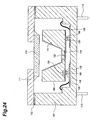
- a P + -type highly-doped semiconductor region 102 and an N + -type highly-doped semiconductor region 103 are formed in the superficial surface layer of an N-type silicon substrate 101 in the superficial surface layer of an N-type silicon substrate 101.
- the P + -type highly-doped semiconductor region 102 and the N + -type highly-doped semiconductor region 103 are connected, respectively, with an anode electrode 104 and a cathode electrode 105.
- bump electrodes 106 made from solder.
- the N-type silicon substrate 101 is thinned in the portion corresponding to the P + -type highly-doped semiconductor region 102 from the rear surface side thereof. The thinned portion functions as an incident part for to-be-detected light.
- the back illuminated photodiode 100 is packed into a ceramic package 107 by flip-chip bonding. That is, the bump electrodes 106 of the back illuminated photodiode 100 are connected to solder pads 109 provided on a bottom wiring 108 of the ceramic package 107. The bottom wiring 108 is connected to output terminal pins 110 through wire bonding. Also, on the surface of the ceramic package 107 is seam-welded a window frame 111 using brazing material 112. In the window frame 111 is formed an opening at the position corresponding to the thinned portion of the back illuminated photodiode 100, and in the opening is provided a transmissive window member 113 such as kovar glass for transmitting to-be-detected light.
- Patent Document 1 Japanese Published Unexamined Patent Application No. H09-219421
- Patent Document 1 a CSP (Chip Size Package) technique for semiconductor electronic components.
- This technique is adapted to seal the both surfaces of a wafer with semiconductor electronic components built therein using organic material such as resin, and then to form an opening in the organic material provided on one surface side of the wafer by photolithography to form electrodes therein.
- the back illuminated photodiode is thinned at the portion that functions as an incident part for to-be-detected light, which reduces the mechanical strength thereof. Therefore, not a pyramid collet but a flat collet is used when assembling the back illuminated photodiode. For example, when heating and pressurizing a bump electrode, etc., provided on the surface side of a photodiode, heat and pressure is added from a heater block while the back illuminated photodiode sticks thereto using a flat collet to employ the rear surface thereof as a sticking surface.
- the resin may be damaged due to contact with the collet. If the resin in the thinned portion (i.e. incident part for to-be-detected light) of the back illuminated photodiode may thus be damaged, there is a problem in that the damage scatters to-be-detected light. Then, the scattering of to-be-detected light also leads to a reduction in the sensitivity of the back illuminated photodiode.
- the present invention has been made to solve the above-described problems, and an object thereof is to provide a back illuminated photodetector having a sufficiently small package as well as being capable of suppressing the scattering of to-be-detected light.
- the present invention is directed to a back illuminated photodetector comprising: a first conductive type semiconductor substrate; a second conductive type doped semiconductor region provided in the first superficial surface layer of the semiconductor substrate; a recessed portion for incidence of to-be-detected light formed in the second surface of the semiconductor substrate and in an area opposite the doped semiconductor region; and a coating layer made of resin for transmitting the to-be-detected light, the coating layer being provided on the second surface, and the coating layer being arranged in such a manner that the portion provided on the recessed portion in the second surface is sunk lower than the portion provided on the outer edge portion of the recessed portion.
- the mechanical strength of the back illuminated photodetector can be increased.
- the increase in mechanical strength allows for dicing at a wafer level, whereby it is possible to obtain a chip-sized back illuminated photodetector. Accordingly, it is possible to achieve a back illuminated photodetector having a sufficiently small package.
- the coating layer is also made of resin for transmitting to-be-detected light not only to increase the mechanical strength of the back illuminated photodetector, but also to function as a transmissive window member for to-be-detected light.
- the coating layer is arranged in such a manner that the portion provided on the recessed portion is sunk lower than the portion provided on the outer edge portion of the recessed portion. Therefore, even if a flat collet may be used in an assembling operation, the surface of the coating layer provided on the recessed portion is not brought into contact with the flat collet. Thus, the incident part for to-be-detected light within the surface of the coating layer cannot be damaged, whereby it is possible to suppress the scattering of to-be-detected light.
- the back illuminated photodetector according to the present invention preferably comprises a supporting film provided on the first surface of the semiconductor substrate to support the semiconductor substrate. In this case, the mechanical strength of the back illuminated photodetector can be increased.
- the back illuminated photodetector preferably comprises a filling electrode penetrating through the supporting film and connected electrically to the doped layer at one end thereof. In this case, it is possible to take a detected signal easily outside the back illuminated photodetector.
- a highly-doped semiconductor region with impurities of the first conductive type added thereto at a high concentration is exposed across the entire side surface of the semiconductor substrate.
- the highly-doped semiconductor region can trap unnecessary carriers that are generated in the vicinity of the side surface of the semiconductor substrate, and therefore can suppress dark current and/or noise.
- a highly-doped semiconductor layer with impurities of the first conductive type added thereto at a high concentration is provided in the bottom portion of the recessed portion within the second superficial surface layer of the semiconductor substrate.
- the highly-doped semiconductor layer functions as an accumulation layer. This can make carriers generated upon incidence of to-be-detected light easy to move toward the first surface of the semiconductor substrate, resulting in an increase in the sensitivity of the back illuminated photodetector.
- a highly-doped semiconductor layer with impurities of the first conductive type added thereto at a high concentration is provided in the second superficial surface layer in the outer edge portion of the semiconductor substrate.
- the highly-doped semiconductor layer can suppress dark current and/or noise due to the crystal defects.
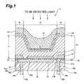
- FIG. 1 is a cross-sectional view showing a first embodiment of a back illuminated photodetector according to the present invention.
- FIG. 1 is a cross-sectional view showing a first embodiment of a back illuminated photodetector according to the present invention.
- the back illuminated photodiode 1 is adapted to receive to-be-detected light from the rear surface thereof, to generate carriers upon incidence of the to-be-detected light, and then to output the generated carriers as a detected signal from the upper surface thereof.
- the back illuminated photodiode 1 comprises an N-type semiconductor substrate 10, a P + -type doped semiconductor region 11, a recessed portion 12, and a coating layer 13.
- the N-type semiconductor substrate 10 for example, a silicon substrate with N-type impurities such as phosphorous added thereto can be used.
- the impurity concentration of the N-type semiconductor substrate 10 is 10 12 to 10 15 /cm 3 , for example.
- the thickness t1 of the N-type semiconductor substrate 10 is 200 ⁇ m to 500 ⁇ m, for example.
- the P + -type doped semiconductor region 11 is provided with P-type impurities such as boron to form a PN junction with the N-type semiconductor substrate 10.
- the impurity concentration of the P + -type doped semiconductor region 11 is 10 15 to 10 20 /cm 3 , for example.
- the depth of the P + -type doped semiconductor region 11 is 0.1 ⁇ m to 20 ⁇ m, for example.
- the recessed portion 12 functions as an incident part for to-be-detected light.
- the recessed portion 12 has a shape that narrows gradually from the rear surface S2 to the upper surface S1. More specifically, the recessed portion 12 may have, for example, a square pyramid shape or a tapered shape that narrows gradually from the rear surface S2 to the upper surface S1.
- the depth of the recessed portion 12 is 2 ⁇ m to 400 ⁇ m, for example.
- the area between the bottom surface S3 of the recessed portion and the P + -type doped semiconductor region 11 within the N-type semiconductor substrate 10 is made thinner than the other areas so that carriers generated upon incidence of to-be-detected light via the rear surface S2 can easily reach near the P + -type doped semiconductor region 11 provided in the surface layer on the upper surface S1 side.
- the thickness of the thinned area is 10 ⁇ m to 200 ⁇ m, for example.
- the coating layer 13 is made of resin transparent to to-be-detected light, that is, having a sufficient transmissivity for the wavelength of to-be-detected light.
- resin epoxy-based, silicon-based, acryl-based or polyimide-based one, or composite material thereof can be cited.
- the coating layer 13 functions as a protective layer for protecting the rear surface S2 as well as a transmissive window member for transmitting to-be-detected light that is made incident into the recessed portion 12.
- the coating layer 13 is arranged in such a manner that the portion provided on the recessed portion 12 is sunk lower than the portion provided on the outer edge portion 14 of the recessed portion 12.
- the surface of the coating layer 13 provided in the portion where the recessed portion 12 is formed gets into the N-type semiconductor substrate 10 side deeper than the surface of the coating layer 13 provided in the outer edge portion 14 of the recessed portion 12.
- the outer edge portion 14 indicates the portion laterally surrounding the recessed portion 12 within the N-type semiconductor substrate 10.
- the thickness of the coating layer 13 on the outer edge portion 14 is 5 ⁇ m to 500 ⁇ m, for example, and preferably 250 ⁇ m.
- the back illuminated photodiode 1 also comprises an N + -type highly-doped semiconductor layer 21, an N + -type highly-doped semiconductor region 22, insulating films 23 and 24, an anode electrode 25, and a cathode electrode 26.
- the N + -type highly-doped semiconductor layer 21 is formed in the entire surface layer on the rear surface S2 side of the N-type semiconductor substrate 10.
- the N + -type highly-doped semiconductor layer 21 is provided with N-type impurities at a concentration higher than in the N-type semiconductor substrate 10.
- the impurity concentration of the N + -type highly-doped semiconductor layer 21 is 10 15 to 10 20 /cm 3 , for example.
- the depth of the N + -type highly-doped semiconductor layer 21 is 0.1 ⁇ m to 20 ⁇ m, for example.
- the N + -type highly-doped semiconductor region 22 is formed in the surface layer on the upper surface S1 side of the N-type semiconductor substrate 10 at a predetermined distance from the P + -type doped semiconductor region 11.
- the N + -type highly-doped semiconductor region 22 is also provided with N-type impurities at a high concentration, as is the case with the N + -type highly-doped semiconductor layer 21, to be a contact layer for the cathode electrode 26 to be described hereinafter as well as to have a function of suppressing surface leakage current in the upper surface S1.
- the impurity concentration of the N + -type highly-doped semiconductor region 22 is 10 15 to 10 20 /cm 3 , for example.
- the depth of the N + -type highly-doped semiconductor region 22 is 0.1 ⁇ m to 30 ⁇ m, for example.
- the insulating films 23 and 24 are formed, respectively, on the upper surface S 1 and the rear surface S2 of the N-type semiconductor substrate 10.
- the insulating films 23 and 24 are made of SiO 2 , for example.
- the thickness of the insulating film 23 is 0.1 ⁇ m to 2 ⁇ m, for example.
- the thickness of the insulating film 24 is 0.05 ⁇ m to 1 ⁇ m, for example.
- openings (contact holes) 23a and 23b one opening 23a being provided within the range of the P + -type doped semiconductor region 11, while the other opening 23b being provided within the range of the N + -type highly-doped semiconductor region 22.
- the anode electrode 25 and the cathode electrode 26 On the insulating film 23 and in the areas including the openings 23a and 23b are formed, respectively, the anode electrode 25 and the cathode electrode 26.
- the thickness of the electrodes 25 and 26 is 1 ⁇ m, for example.
- the electrodes 25 and 26 are provided in such a manner as to fill the respective openings 23a and 23b.
- the anode electrode 25 is connected directly to the P + -type doped semiconductor region 11 through the opening 23a
- the cathode electrode 26 is connected directly to the N + -type highly-doped semiconductor region 22 through the opening 23b.
- Al can be used as the anode and cathode electrodes 25 and 26, for example, Al.
- the back illuminated photodiode 1 further comprises a passivation film 31, a supporting film 32, filling electrodes 33a and 33b, UBMs (Under Bump Metals) 34a and 34b, and bumps 35a and 35b.
- the passivation film 31 is provided on the upper surface S1 of the N-type semiconductor substrate 10 in such a manner as to cover the insulating film 23, anode electrode 25, and cathode electrode 26. Also, in the portions provided on the anode electrode 25 and the cathode electrode 26 within the passivation film 31 are formed through holes 31a to be filled with the filling electrodes 33a and 33b to be described hereinafter.
- the passivation film 31 is made of SiN, for example, to protect the upper surface S1 of the N-type semiconductor substrate 10.
- the passivation film 31 can be formed by, for example, a plasma-CVD method. Also, the thickness of the passivation film 31 is 1 ⁇ m, for example.
- the supporting film 32 On the passivation film 31 is formed the supporting film 32.
- the supporting film 32 is adapted to support the N-type semiconductor substrate 10. Also, in the portions corresponding to the through holes 31a in the passivation film 31 within the supporting film 32 are formed through holes 32a to be filled with the filling electrodes 33a and 33b that also fill the through holes 31a.
- a material of the supporting film 32 for example, resin or SiO 2 , etc., that can be formed by, for example, a plasma-CVD method can be used.
- the thickness of the supporting film 32 is 2 ⁇ m to 100 ⁇ m, for example, and preferably about 50 ⁇ m.
- the filling electrodes 33a and 33b fill the through holes 31a and 32a, and are brought into contact, respectively, with the anode electrode 25 and the cathode electrode 26 at one end thereof to be connected electrically to the P + -type doped semiconductor region 11 and the N + -type highly-doped semiconductor region 22. Also, the other end of the filling electrodes 33a and 33b is exposed at the surface of the supporting film 32. That is, the filling electrodes 33a and 33b penetrate through the passivation film 31 and the supporting film 32 to extend, respectively, from the anode electrode 25 and the cathode electrode 26 to the surface of the supporting film 32. In addition, the filling electrodes 33a and 33b each have an approximately cylindrical shape.
- the filling electrodes 33a and 33b are adapted to connect, respectively, the electrodes 25 and 26 and the bumps 35a and 35b to be described hereinafter electrically with each other.
- the filling electrodes 33a and 33b are made of Cu, for example.
- the diameter of the through holes 31a and 32a is 10 ⁇ m to 200 ⁇ m, for example, and preferably about 100 ⁇ m.
- the UBMs 34a and 34b are composed of accumulation films made ofNi and Au, for example. Also, the thickness of the UBMs 34a and 34b is 0.1 ⁇ m to 5 ⁇ m, for example.
- the bumps 35a and 35b are formed on the surfaces of the UBMs 34a and 34b on the opposite side of the filling electrodes 33a and 33b.
- the bumps 35a and 35b are therefore connected, respectively, to the anode electrode 25 and the cathode electrode 26 electrically.
- the bumps 35a and 35b each have an approximately spherical shape except for the surfaces in contact with the UBMs 34a and 34b.
- solder, gold, Ni-Au, Cu, or resin containing metal filler can be used as the bumps 35a and 35b.
- the back illuminated photodiode 1 is applied with a reverse bias voltage, and that there is generated a depletion layer in the thinned area in the N-type semiconductor substrate 10.
- to-be-detected light penetrates through the coating layer 13 and then enters the N-type semiconductor substrate 10 from the recessed portion 12, the light is absorbed mainly in the thinned area. Accordingly, in the area, carriers (holes and electrons) are generated. The generated holes and electrons are moved, respectively, to the P + -type doped semiconductor region 11 and the N + -type highly-doped semiconductor region 22 in accordance with the reverse bias electric field.
- Holes and electrons that have reached the P + -type doped semiconductor region 11 and the N + -type highly-doped semiconductor region 22 are moved to the bumps 35a and 35b from the filling electrodes 33a and 33b and the UBMs 34a and 34b to be output as a detected signal from the bumps 35a and 35b.
- the mechanical strength of the back illuminated photodiode 1 is increased.
- the coating layer 13 is provided on the recessed portion 12, it is possible to prevent the thinned area in the N-type semiconductor substrate 10 from being distorted, flexed or damaged even if pressure and/or heat may be applied to the back illuminated photodiode 1 in an assembling operation.
- the increase in mechanical strength allows for dicing at a wafer level, whereby it is possible to obtain a chip-sized back illuminated photodiode 1. Accordingly, there is achieved a back illuminated photodiode 1 having a sufficiently small package.
- the coating layer 13 is arranged in such a manner that the portion provided on the recessed portion 12 is sunk lower than the portion provided on the outer edge portion 14 of the recessed portion 12. Therefore, even if a flat collet FC may be used in an assembling operation as shown in FIG. 2, the surface of the coating layer 13 provided on the recessed portion 12 is not brought into contact with the flat collet FC. Thus, the incident part for to-be-detected light within the surface of the coating layer 13 cannot be damaged, whereby it is possible to suppress the scattering of to-be-detected light. Thus, a highly sensitive back illuminated photodiode 1 is achieved.
- providing the coating layer 13 also on the outer edge portion 14 prevents the flat collet FC from being brought into direct contact with the outer edge portion 14. It is thus possible to prevent the generation of crystal defects in the outer edge portion 14 due to contact with the flat collet FC, and therefore to suppress dark current and/or noise due to the crystal defects.
- the coating layer 13 resin is used, which makes it easy to form the coating layer 13 into a desired shape.
- the provided supporting film 32 further increases the mechanical strength of the back illuminated photodiode 1.
- the provided filling electrodes 33a and 33b make it easy to take a detected signal outside from the electrodes 25 and 26. Additionally, the filling electrodes 33a and 33b may be formed on the sidewalls of the through holes 31a and 32a to be connected electrically to the anode electrode 25 and the cathode electrode 26.
- the N + -type highly-doped semiconductor layer 21 is formed in the entire surface layer on the rear surface S2 side of the N-type semiconductor substrate 10.
- the N + -type highly-doped semiconductor layer 21 provided in the bottom surface S3 of the recessed portion 12 within the surface layer of the rear surface S2 functions as an accumulation layer. This can prevent carriers generated in the N-type semiconductor substrate 10 from being recombined in the vicinity of the bottom surface S3. Thus, a more highly sensitive back illuminated photodiode 1 is achieved.
- the impurity concentration of the N + -type highly-doped semiconductor layer 21 is preferably 10 15 /cm 3 or more. In this case, the N + -type highly-doped semiconductor layer 21 can suitably function as an accumulation layer.
- the N + -type highly-doped semiconductor layer 21, which is provided in the surface layer on the rear surface S2 side within the outer edge portion 14 of the N-type semiconductor substrate 10, can suppress dark current and/or noise due to the crystal defects. Therefore, in accordance with the back illuminated photodiode 1, it is possible to obtain a detected signal at a high S/N ratio.
- the impurity concentration of the N + -type highly-doped semiconductor layer 21 is preferably 10 15 /cm 3 or more. In this case, the N + -type highly-doped semiconductor layer 21 can suppress dark current and/or noise due to crystal defects sufficiently.
- an exemplary method for manufacturing the back illuminated photodiode 1 shown in FIG. 1 will here be described with reference to FIG. 3 to FIG. 17.
- an N-type semiconductor substrate 10 made of an N-type silicon wafer with the upper surface S 1 and the rear surface S2 thereof being formed into (100) planes.
- the N-type semiconductor substrate 10 is thermally oxidized to form an insulating film made of SiO 2 on the upper surface S 1 of the N-type semiconductor substrate 10.
- openings are formed openings, and then phosphorous is doped into the N-type semiconductor substrate 10 from the openings to form N + -type highly-doped semiconductor regions 22.
- the N-type semiconductor substrate 10 is oxidized to form an insulating film on the upper surface S1. Similarly, in predetermined portions of the insulating film are formed openings, and then boron is doped into the N-type semiconductor substrate 10 from the openings to form P + -type doped semiconductor regions 11. Subsequently, the N-type semiconductor substrate 10 is oxidized to form an insulating film 23 on the upper surface S1 (FIG. 3).
- the rear surface S2 of the N-type semiconductor substrate 10 is polished, and SiN 82 is deposited on the rear surface S2 of the N-type semiconductor substrate 10 by LP-CVD (FIG. 4). Also, in the SiN 82 on the rear surface S2 are formed openings 85 to form recessed portions 12 (FIG. 5). Then, an etching operation is performed using KOH, etc., through the openings 85 to form recessed portions 12 (FIG. 6).
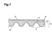
- the SiN 82 is removed, ion implantation, etc., is performed onto the rear surface S2 side of the N-type semiconductor substrate 10 with the recessed portions 12 formed therein to dope N-type impurities and thereby to form an N + -type highly-doped semiconductor layer 21 in the entire surface layer on the rear surface S2 side (FIG. 7).
- the substrate is thermally oxidized to form an insulating film 24 in the entire surface layer on the rear surface S2 side (FIG. 8).
- Contact holes for electrodes are formed in the insulating film 23 on the upper surface S1, and after aluminum is deposited on the upper surface S1, a predetermined pattern is made to form anode electrodes 25 and cathode electrodes 26 (FIG. 9).
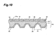
- a passivation film 31 made of SiN is deposited on the upper surface S1 of the N-type semiconductor substrate 10, on which the anode electrodes 25 and the cathode electrodes 26 are formed, by a plasma-CVD method. Also, openings 31a are formed in portions corresponding to bumps 35a and 35b within the passivation film 31 (FIG. 10). Further, a thick supporting film 32 made of resin is formed on the upper surface S1, and openings 32a are formed in the portions corresponding to the openings 31 a in the passivation film 31.
- resin such as epoxy-based, acryl-based or polyimide-based one can be used. Alternatively, SiO 2 formed by plasma-CVD, etc., may be used.
- the openings 32a in the supporting film 32 can be formed by a photolithography method using, for example, photosensitive resin or by a patterning process such as etching (FIG. 11).
- a conductive material 33 made of Cu is deposited in such a manner as to fill the openings 31a and 32a. This can be made through the steps of, for example, depositing a Cu seed layer, etc., by sputtering, etc., on the surface of the anode electrodes 25 and the cathode electrodes 26 that are exposed from the openings 31a and 32a, and depositing Cu, etc., by plating on the Cu seed layer (FIG. 12).
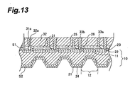
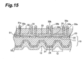
- filling electrodes 33a and 33b are formed (FIG. 13). Also, after a coating layer 13 made of resin is applied by spin coating or printing, etc., in such a manner as to fully cover the rear surface S2, the applied coating layer 13 is hardened. Here, the portion of the coating layer 13 provided on the recessed portion 12 is to be sunk (FIG. 14). Further, UBMs 34a and 34b composed of accumulation films made of Ni and Au, etc., are formed on the filling electrodes 33a and 33b on the upper surface S1 by electroless plating. In addition, bumps 35a and 35b made of solder, etc., are formed on the UBMs 34a and 34b by printing or a ball-mounting method, etc., (FIG. 15).
- FIG. 18 is a cross-sectional view showing a second embodiment of a back illuminated photodetector according to the present invention.
- the back illuminated photodiode 2 comprises a semiconductor substrate 20, a P + -type doped semiconductor region 11, a recessed portion 12, and a coating layer 13.
- the P + -type doped semiconductor region 11 In the surface layer on the upper surface S 1 side of the semiconductor substrate 20 is partially formed the P + -type doped semiconductor region 11. Meanwhile, in the rear surface S2 of the semiconductor substrate 20 and in an area opposite the P + -type doped semiconductor region 11 is formed the recessed portion 12. Also, on the rear surface S2 of the semiconductor substrate 20 is provided the coating layer 13. The coating layer 13 is arranged in such a manner that the portion provided on the recessed portion 12 is sunk lower than the portion provided on the outer edge portion 14 of the recessed portion 12.
- the back illuminated photodiode 2 also comprises an N + -type highly-doped semiconductor region 28, insulating films 23 and 24, an anode electrode 25, and a cathode electrode 26.
- the N + -type highly-doped semiconductor region 28 is formed in such a manner as to be exposed at the entire side surfaces S4 of the semiconductor substrate 20.
- the N + -type highly-doped semiconductor region 28 also reaches the entire rear surface S2 of the semiconductor substrate 20.
- the portion 20a within the semiconductor substrate 20, in which neither the P + -type doped semiconductor region 11 nor the N + -type highly-doped semiconductor region 28 is formed, is surrounded entirely by the N + -type highly-doped semiconductor region 28 from the side surface S4 sides and the rear surface S2 side of the semiconductor substrate 20.
- N + -type highly-doped semiconductor region 28 there is prepared a semiconductor substrate 20.
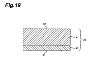
- an N + -type highly-doped semiconductor layer 41 is diffused from the rear surface S2 with a part on the upper surface S1 side remaining.
- the remaining part on the upper surface S1 side is an N-type doped semiconductor layer 42 having an impurity concentration lower than that of the N + -type highly-doped semiconductor layer 41 (FIG. 19).
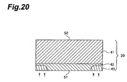
- N-type impurities are doped at a high concentration from the upper surface S1 side to form N + -type highly-doped semiconductor regions 43 (FIG. 20).
- the N-type impurities are diffused further deeply by heat treatment so that the N + -type highly-doped semiconductor regions 43 reach the N + -type highly-doped semiconductor layer 41 (FIG. 21).
- an N + -type highly-doped semiconductor region 28 composed of the N + -type highly-doped semiconductor layer 41 and the N + -type highly-doped semiconductor regions 43.
- the areas where a P + -type doped semiconductor region 11 and a recessed portion 12 are to be formed are indicated, respectively, by the dashed lines L2 and L3.
- the manufacturing process for the N + -type highly-doped semiconductor region 28 and therefore for the entire back illuminated photodiode 2 is simplified.
- the insulating films 23 and 24 are formed, respectively, the insulating films 23 and 24. Also, in the insulating film 23 are formed openings 23a and 23b, one opening 23a being provided within the range of the P + -type doped semiconductor region 11, while the other opening 23b being provided within the range of the N + -type highly-doped semiconductor region 28.
- the anode electrode 25 and the cathode electrode 26 are formed on the insulating film 23 and in the areas including the openings 23a and 23b.
- the electrodes 25 and 26 are provided in such a manner as to fill the respective openings 23a and 23b.
- the anode electrode 25 is connected directly to the P + -type doped semiconductor region 11 through the opening 23a
- the cathode electrode 26 is connected directly to the N + -type highly-doped semiconductor region 28 through the opening 23b.
- the back illuminated photodiode 2 further comprises a passivation film 31, a supporting film 32, filling electrodes 33a and 33b, UBMs 34a and 34b, and bumps 35a and 35b.
- the passivation film 31 is provided on the upper surface S1 of the semiconductor substrate 20 in such a manner as to cover the insulating film 23, anode electrode 25, and cathode electrode 26.
- On the passivation film 31 is formed the supporting film 32.
- the filling electrodes 33a and 33b penetrate through the passivation film 31 and the supporting film 32 to extend, respectively, from the anode electrode 25 and the cathode electrode 26 to the surface of the supporting film 32.
- the UBMs 34a and 34b On the exposed portions of the filling electrodes 33a and 33b at the surface of the supporting film 32 are formed the UBMs 34a and 34b. On the surfaces of the UBMs 34a and 34b on the opposite side of the filling electrodes 33a and 33b are formed the bumps 35a and 35b.
- the mechanical strength of the back illuminated photodiode 2 is increased. Also, the increase in mechanical strength allows for dicing at a wafer level, whereby it is possible to obtain a chip-sized back illuminated photodiode 2. Accordingly, there is achieved a back illuminated photodiode 2 having a sufficiently small package.
- the coating layer 13 is arranged in such a manner that the portion provided on the recessed portion 12 is sunk lower than the portion provided on the outer edge portion 14 of the recessed portion 12. Therefore, even if a flat collet may be used in an assembling operation, the surface of the coating layer 13 provided on the recessed portion 12 is not brought into contact with the flat collet. Thus, the incident part for to-be-detected light within the surface of the coating layer 13 cannot be damaged, whereby it is possible to suppress the scattering of to-be-detected light. Thus, a highly sensitive back illuminated photodiode 2 is achieved.
- the N + -type highly-doped semiconductor region 28 is formed in such a manner as to be exposed at the entire side surfaces S4 of the semiconductor substrate 20.
- the N + -type highly-doped semiconductor region 28 can trap unnecessary carriers that are generated in the vicinity of the side surfaces S4 of the semiconductor substrate 20 and thereby can suppress dark current and/or noise.
- the side surfaces S4 correspond to dicing lines whereby there is a possibility of causing crystal defects in dicing
- the N + -type highly-doped semiconductor region 28 can also suppress dark current and/or noise due to the crystal defects. Therefore, in accordance with the back illuminated photodiode 2, it is possible to obtain a detected signal at a higher S/N ratio.
- the portion 20a within the semiconductor substrate 20 is surrounded entirely by the N + -type highly-doped semiconductor region 28 from the side surface S4 sides and the rear surface S2 side of the semiconductor substrate 20.
- a PIN structure in which the surrounded portion 20a is employed as an I-layer is achieved.
- the back illuminated photodiode 2 can be provided with a higher voltage and thereby can increase the width of the depletion layer due to such a PIN structure, which can increase the sensitivity as well as reduce the capacity thereof to achieve a high-speed response.
- FIG. 22 is a plan view showing a third embodiment of a back illuminated photodetector according to the present invention.
- the back illuminated photodiode array 3 is composed of a total of sixty-four back illuminated photodiodes that are arranged in an eight-by-eight grid pattern. The arrangement pitch of these photodiodes is 1mm, for example.
- FIG. 22 shows the appearance of the back illuminated photodiode array 3 when viewed from the rear surface side.
- the rear surface of each photodiode is covered with a coating layer, and is formed in such a manner that predetermined portions of the coating layer are sunk, as is the case with the back illuminated photodiode 1 shown in FIG. 1.
- the sunk portions of the coating layer are indicated by the dashed lines L4.
- FIG. 23 is a cross-sectional view of the back illuminated photodiode array 3 shown in FIG 22 along the line XII-XII. In the cross-sectional view are shown two photodiodes P1 and P2 among the sixty-four photodiodes shown in FIG. 22.
- the back illuminated photodiode array 3 comprises an N-type semiconductor substrate 50, a P + -type doped semiconductor region 51, a recessed portion 52, and a coating layer 53.
- each P + -type doped semiconductor region 51 is 0.75 ⁇ 0.75mm 2 , for example.
- the recessed portion 52 is formed in the rear surface S2 of the N-type semiconductor substrate 50 and in an area opposite the P + -type doped semiconductor region 51.
- a plurality of the recessed portions 52 being provided with a plurality of the P + -type doped semiconductor regions 51.
- each of the photodiodes P1 and P2 are provided a pair of a P + -type doped semiconductor region 51 and a recessed portion 52. Also, on the rear surface S2 of the N-type semiconductor substrate 50 is provided the coating layer 53. The coating layer 53 is arranged in such a manner that the portion provided on the recessed portion 52 is sunk lower than the portion provided on the outer edge portion 54 of the recessed portion 52.
- the back illuminated photodiode array 3 also comprises an N + -type highly-doped semiconductor layer 61, N + -type highly-doped semiconductor regions 62, insulating films 63 and 64, anode electrodes 65, and cathode electrodes 66.
- the N + -type highly-doped semiconductor layer 61 is formed in the entire surface layer on the rear surface S2 side of the N-type semiconductor substrate 50.
- the N + -type highly-doped semiconductor regions 62 are formed in the surface layer on the upper surface S1 side of the N-type semiconductor substrate 50.
- the N + -type highly-doped semiconductor regions 62 are preferably provided in such a manner as to surround the P + -type doped semiconductor regions 51 constituting the respective photodiodes.
- the insulating films 63 and 64 On the upper surface S1 and the rear surface S2 of the N-type semiconductor substrate 50 are formed, respectively, the insulating films 63 and 64.
- the insulating film 63 In the insulating film 63 are formed openings 63a and 63b, some openings 63a being provided within the range of the P + -type doped semiconductor regions 51, while the other openings 63b being provided within the range of the N + -type highly-doped semiconductor regions 62.
- the anode electrodes 65 and the cathode electrodes 66 On the insulating film 63 and in the areas including the openings 63a and 63b are formed, respectively, the anode electrodes 65 and the cathode electrodes 66.
- the anode electrodes 65 are connected directly to the P + -type doped semiconductor regions 51 through the respective openings 63a, while the cathode electrodes 66 are connected directly to the N + -type highly-doped semiconductor regions 62 through the respective openings 63b.
- the back illuminated photodiode array 3 further comprises a passivation film 71, a supporting film 72, filling electrodes 73a and 73b, UBMs 74a and 74b, and bumps 75a and 75b.
- the passivation film 71 is provided on the upper surface S1 of the N-type semiconductor substrate 50 in such a manner as to cover the insulating film 63, anode electrodes 65, and cathode electrodes 66.
- On the passivation film 71 is formed the supporting film 72.
- the filling electrodes 73a and 73b penetrate through the passivation film 71 and the supporting film 72 to extend, respectively, from the anode electrodes 65 and the cathode electrodes 66 to the surface of the supporting film 72.
- the UBMs 74a and 74b On the exposed portions of the filling electrodes 73a and 73b at the surface of the supporting film 72 are formed the UBMs 74a and 74b. On the surfaces of the UBMs 74a and 74b on the opposite side of the filling electrodes 73a and 73b are formed the bumps 75a and 75b.
- the mechanical strength of the back illuminated photodiode array 3 is increased. Also, the increase in mechanical strength allows for dicing at a wafer level, whereby it is possible to obtain a chip-sized back illuminated photodiode array 3. Accordingly, there is achieved a back illuminated photodiode array 3 having a sufficiently small package.
- the coating layer 53 is arranged in such a manner that the portions provided on the recessed portions 52 are sunk lower than the portions provided on the outer edge portions 54 of the recessed portions 52. Therefore, even if a flat collet may be used in an assembling operation, the surface of the coating layer 53 provided on the recessed portions 52 is not brought into contact with the flat collet. Thus, the incident parts for to-be-detected light within the surface of the coating layer 53 cannot be damaged, whereby it is possible to suppress the scattering of to-be-detected light. Thus, a highly sensitive back illuminated photodiode array 3 is achieved.
- the back illuminated photodiode array 3 can suitably be used for an image sensor, etc., in which each photodiode represents one pixel.
- the back illuminated photodetector according to the present invention is not restricted to the above-described embodiments, and various modifications may be made.
- a P-type semiconductor substrate may be used instead of the N-type semiconductor substrate 10.
- the doped semiconductor region 11 has N-type conductivity
- the highly-doped semiconductor layer 21 and the highly-doped semiconductor region 22 have P-type conductivity.
- FIG. 12 is shown an example of depositing a conductive material 33 made of Cu
- Ni may be used instead of Cu to perform electroless plating of Ni directly on the surface of the anode electrodes 25 and the cathode electrodes 26 that are exposed from the openings 31a and 32a. In this case, it is possible to omit the step of polishing the surface of the conductive material 33 illustrated in FIG. 13.
- a bonded wafer in which an N + -type highly-doped semiconductor layer and an N-type doped semiconductor layer having an impurity concentration lower than that of the N + -type highly-doped semiconductor layer are bonded to each other may be used.
- the N-type doped semiconductor layer is to be provided on the upper surface S1 side, while the N + -type highly-doped semiconductor layer on the rear surface S2 side of the semiconductor substrate 20.
Landscapes
- Light Receiving Elements (AREA)
- Solid State Image Pick-Up Elements (AREA)
Abstract
Description
- The present invention relates to a back illuminated photodetector.
- In such a conventional back illuminated
photodiode 100 as shown in FIG 24, in the superficial surface layer of an N-type silicon substrate 101 are formed a P+-type highly-dopedsemiconductor region 102 and an N+-type highly-dopedsemiconductor region 103. The P+-type highly-dopedsemiconductor region 102 and the N+-type highly-dopedsemiconductor region 103 are connected, respectively, with ananode electrode 104 and acathode electrode 105. On theelectrodes bump electrodes 106 made from solder. Also, the N-type silicon substrate 101 is thinned in the portion corresponding to the P+-type highly-dopedsemiconductor region 102 from the rear surface side thereof. The thinned portion functions as an incident part for to-be-detected light. - As shown in FIG 24, the back illuminated
photodiode 100 is packed into aceramic package 107 by flip-chip bonding. That is, thebump electrodes 106 of the back illuminatedphotodiode 100 are connected tosolder pads 109 provided on abottom wiring 108 of theceramic package 107. Thebottom wiring 108 is connected tooutput terminal pins 110 through wire bonding. Also, on the surface of theceramic package 107 is seam-welded awindow frame 111 usingbrazing material 112. In thewindow frame 111 is formed an opening at the position corresponding to the thinned portion of the back illuminatedphotodiode 100, and in the opening is provided atransmissive window member 113 such as kovar glass for transmitting to-be-detected light.
Patent Document 1: Japanese Published Unexamined Patent Application No. H09-219421 - However, in such an arrangement of using a ceramic package in a back illuminated photodiode as above, there is a problem in that the package becomes larger.
- Meanwhile, in
Patent Document 1 is disclosed a CSP (Chip Size Package) technique for semiconductor electronic components. This technique is adapted to seal the both surfaces of a wafer with semiconductor electronic components built therein using organic material such as resin, and then to form an opening in the organic material provided on one surface side of the wafer by photolithography to form electrodes therein. - However, trying to apply such a CSP technique to a back illuminated photodiode to reduce the package size leads to the following problem. That is, the back illuminated photodiode is thinned at the portion that functions as an incident part for to-be-detected light, which reduces the mechanical strength thereof. Therefore, not a pyramid collet but a flat collet is used when assembling the back illuminated photodiode. For example, when heating and pressurizing a bump electrode, etc., provided on the surface side of a photodiode, heat and pressure is added from a heater block while the back illuminated photodiode sticks thereto using a flat collet to employ the rear surface thereof as a sticking surface.
- In the case of using a flat collet for a back illuminated photodiode with the rear surface being sealed with resin, the resin may be damaged due to contact with the collet. If the resin in the thinned portion (i.e. incident part for to-be-detected light) of the back illuminated photodiode may thus be damaged, there is a problem in that the damage scatters to-be-detected light. Then, the scattering of to-be-detected light also leads to a reduction in the sensitivity of the back illuminated photodiode.
- The present invention has been made to solve the above-described problems, and an object thereof is to provide a back illuminated photodetector having a sufficiently small package as well as being capable of suppressing the scattering of to-be-detected light.
- In order to solve the above-described problem, the present invention is directed to a back illuminated photodetector comprising: a first conductive type semiconductor substrate; a second conductive type doped semiconductor region provided in the first superficial surface layer of the semiconductor substrate; a recessed portion for incidence of to-be-detected light formed in the second surface of the semiconductor substrate and in an area opposite the doped semiconductor region; and a coating layer made of resin for transmitting the to-be-detected light, the coating layer being provided on the second surface, and the coating layer being arranged in such a manner that the portion provided on the recessed portion in the second surface is sunk lower than the portion provided on the outer edge portion of the recessed portion.
- In the back illuminated photodetector, since there is provided the coating layer, the mechanical strength of the back illuminated photodetector can be increased. The increase in mechanical strength allows for dicing at a wafer level, whereby it is possible to obtain a chip-sized back illuminated photodetector. Accordingly, it is possible to achieve a back illuminated photodetector having a sufficiently small package. The coating layer is also made of resin for transmitting to-be-detected light not only to increase the mechanical strength of the back illuminated photodetector, but also to function as a transmissive window member for to-be-detected light.
- Further, the coating layer is arranged in such a manner that the portion provided on the recessed portion is sunk lower than the portion provided on the outer edge portion of the recessed portion. Therefore, even if a flat collet may be used in an assembling operation, the surface of the coating layer provided on the recessed portion is not brought into contact with the flat collet. Thus, the incident part for to-be-detected light within the surface of the coating layer cannot be damaged, whereby it is possible to suppress the scattering of to-be-detected light.
- The back illuminated photodetector according to the present invention preferably comprises a supporting film provided on the first surface of the semiconductor substrate to support the semiconductor substrate. In this case, the mechanical strength of the back illuminated photodetector can be increased.
- Further, the back illuminated photodetector preferably comprises a filling electrode penetrating through the supporting film and connected electrically to the doped layer at one end thereof. In this case, it is possible to take a detected signal easily outside the back illuminated photodetector.
- It is preferable that a highly-doped semiconductor region with impurities of the first conductive type added thereto at a high concentration is exposed across the entire side surface of the semiconductor substrate. In this case, even if a side surface of the semiconductor substrate may be damaged through dicing, etc., the highly-doped semiconductor region can trap unnecessary carriers that are generated in the vicinity of the side surface of the semiconductor substrate, and therefore can suppress dark current and/or noise.
- It is preferred that a highly-doped semiconductor layer with impurities of the first conductive type added thereto at a high concentration is provided in the bottom portion of the recessed portion within the second superficial surface layer of the semiconductor substrate. The highly-doped semiconductor layer functions as an accumulation layer. This can make carriers generated upon incidence of to-be-detected light easy to move toward the first surface of the semiconductor substrate, resulting in an increase in the sensitivity of the back illuminated photodetector.
- It is preferable that a highly-doped semiconductor layer with impurities of the first conductive type added thereto at a high concentration is provided in the second superficial surface layer in the outer edge portion of the semiconductor substrate. In this case, even if there may be crystal defects in the vicinity of the second superficial surface in the outer edge portion, the highly-doped semiconductor layer can suppress dark current and/or noise due to the crystal defects.
- In accordance with the present invention, it is possible to achieve a back illuminated photodetector having a sufficiently small package as well as being capable of suppressing the scattering of to-be-detected light.
- FIG. 1 is a cross-sectional view showing a first embodiment of a back illuminated photodetector according to the present invention.
- FIG. 2 is a view illustrating the effect of the back illuminated
photodiode 1 shown in FIG. 1. - FIG. 3 is a step chart showing a method for manufacturing the back illuminated
photodiode 1 shown in FIG. 1. - FIG. 4 is a step chart showing a method for manufacturing the back illuminated
photodiode 1 shown in FIG. 1. - FIG. 5 is a step chart showing a method for manufacturing the back illuminated
photodiode 1 shown in FIG. 1. - FIG. 6 is a step chart showing a method for manufacturing the back illuminated
photodiode 1 shown in FIG. 1. - FIG. 7 is a step chart showing a method for manufacturing the back illuminated
photodiode 1 shown in FIG. 1. - FIG. 8 is a step chart showing a method for manufacturing the back illuminated
photodiode 1 shown in FIG. 1. - FIG. 9 is a step chart showing a method for manufacturing the back illuminated
photodiode 1 shown in FIG. 1. - FIG. 10 is a step chart showing a method for manufacturing the back illuminated
photodiode 1 shown in FIG. 1. - FIG. 11 is a step chart showing a method for manufacturing the back illuminated
photodiode 1 shown in FIG. 1. - FIG. 12 is a step chart showing a method for manufacturing the back illuminated
photodiode 1 shown in FIG. 1. - FIG. 13 is a step chart showing a method for manufacturing the back illuminated
photodiode 1 shown in FIG. 1. - FIG. 14 is a step chart showing a method for manufacturing the back illuminated
photodiode 1 shown in FIG. 1. - FIG. 15 is a step chart showing a method for manufacturing the back illuminated
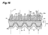
photodiode 1 shown in FIG. 1. - FIG. 16 is a step chart showing a method for manufacturing the back illuminated
photodiode 1 shown in FIG. 1. - FIG. 17 is a step chart showing a method for manufacturing the back illuminated
photodiode 1 shown in FIG. 1. - FIG. 18 is a cross-sectional view showing a second embodiment of a back illuminated photodetector according to the present invention.
- FIG. 19 is a view illustrating an exemplary method for forming the N+-type highly-doped
semiconductor region 28 shown in FIG. 18. - FIG. 20 is a view illustrating an exemplary method for forming the N+-type highly-doped
semiconductor region 28 shown in FIG. 18. - FIG. 21 is a view illustrating an exemplary method for forming the N+-type highly-doped
semiconductor region 28 shown in FIG. 18. - FIG. 22 is a plan view showing a third embodiment of a back illuminated photodetector according to the present invention.
- FIG. 23 is a cross-sectional view of the back illuminated
photodiode array 3 shown in FIG. 22 along the line XII-XII. - FIG. 24 is a cross-sectional view of a conventional back illuminated photodiode.
- 1 and 2: Back illuminated photodiodes, 3: Back illuminated photodiode array, 10 and 50: N-type semiconductor substrates, 11 and 51: P+-type doped semiconductor regions, 12 and 52: Recessed portions, 13 and 53: Coating layers, 14 and 54: Outer edge portions, 20: Semiconductor substrate, 21 and 61: N+-type highly-doped semiconductor layers, 22; 28 and 62: N+-type highly-doped semiconductor regions, 23; 24; 63 and 64: Insulating films, 25 and 65: Anode electrodes, 26 and 66: Cathode electrodes, 31 and 71: Passivation films, 32 and 72: Supporting films, 33a; 33b; 73a and 73b: Filling electrodes, 34a; 34b; 74a and 74b: UBMs, 35a; 35b; 75a and 75b: Bumps, S1: Upper surface, S2: Rear surface, S3: Bottom surface of recessed portion, S4: Side surface of the
semiconductor substrate 20 - Preferred embodiments of a back illuminated photodetector according to the present invention will hereinafter be described in detail with reference to the accompanying drawings. Additionally, in the descriptions of the drawings, identical components are designated by the same reference numerals to omit overlapped description. Also, the dimensional ratios in the drawings do not necessarily correspond to those in the descriptions.
- FIG. 1 is a cross-sectional view showing a first embodiment of a back illuminated photodetector according to the present invention. The back illuminated
photodiode 1 is adapted to receive to-be-detected light from the rear surface thereof, to generate carriers upon incidence of the to-be-detected light, and then to output the generated carriers as a detected signal from the upper surface thereof. The back illuminatedphotodiode 1 comprises an N-type semiconductor substrate 10, a P+-type dopedsemiconductor region 11, a recessedportion 12, and acoating layer 13. As the N-type semiconductor substrate 10, for example, a silicon substrate with N-type impurities such as phosphorous added thereto can be used. The impurity concentration of the N-type semiconductor substrate 10 is 1012 to 1015/cm3, for example. Also, the thickness t1 of the N-type semiconductor substrate 10 is 200µm to 500µm, for example. - In the surface layer on the upper surface (first surface) S1 side of the N-
type semiconductor substrate 10 is partially formed the P+-type dopedsemiconductor region 11. The P+-type dopedsemiconductor region 11 is provided with P-type impurities such as boron to form a PN junction with the N-type semiconductor substrate 10. The impurity concentration of the P+-type dopedsemiconductor region 11 is 1015 to 1020/cm3, for example. Also, the depth of the P+-type dopedsemiconductor region 11 is 0.1µm to 20µm, for example. - In the rear surface (second surface) S2 of the N-
type semiconductor substrate 10 and in an area opposite the P+-type dopedsemiconductor region 11 is formed the recessedportion 12. The recessedportion 12 functions as an incident part for to-be-detected light. The recessedportion 12 has a shape that narrows gradually from the rear surface S2 to the upper surface S1. More specifically, the recessedportion 12 may have, for example, a square pyramid shape or a tapered shape that narrows gradually from the rear surface S2 to the upper surface S1. The depth of the recessedportion 12 is 2µm to 400µm, for example. Also, due to the thus formed recessedportion 12, the area between the bottom surface S3 of the recessed portion and the P+-type dopedsemiconductor region 11 within the N-type semiconductor substrate 10 is made thinner than the other areas so that carriers generated upon incidence of to-be-detected light via the rear surface S2 can easily reach near the P+-type dopedsemiconductor region 11 provided in the surface layer on the upper surface S1 side. In addition, the thickness of the thinned area is 10µm to 200µm, for example. - On the rear surface S2 of the N-
type semiconductor substrate 10 is provided thecoating layer 13. Thecoating layer 13 is made of resin transparent to to-be-detected light, that is, having a sufficient transmissivity for the wavelength of to-be-detected light. As such resin epoxy-based, silicon-based, acryl-based or polyimide-based one, or composite material thereof can be cited. Thecoating layer 13 functions as a protective layer for protecting the rear surface S2 as well as a transmissive window member for transmitting to-be-detected light that is made incident into the recessedportion 12. Also, thecoating layer 13 is arranged in such a manner that the portion provided on the recessedportion 12 is sunk lower than the portion provided on theouter edge portion 14 of the recessedportion 12. That is, the surface of thecoating layer 13 provided in the portion where the recessedportion 12 is formed gets into the N-type semiconductor substrate 10 side deeper than the surface of thecoating layer 13 provided in theouter edge portion 14 of the recessedportion 12. Herein, theouter edge portion 14 indicates the portion laterally surrounding the recessedportion 12 within the N-type semiconductor substrate 10. The thickness of thecoating layer 13 on theouter edge portion 14 is 5µm to 500µm, for example, and preferably 250µm. - The back illuminated
photodiode 1 also comprises an N+-type highly-dopedsemiconductor layer 21, an N+-type highly-dopedsemiconductor region 22, insulatingfilms anode electrode 25, and acathode electrode 26. The N+-type highly-dopedsemiconductor layer 21 is formed in the entire surface layer on the rear surface S2 side of the N-type semiconductor substrate 10. The N+-type highly-dopedsemiconductor layer 21 is provided with N-type impurities at a concentration higher than in the N-type semiconductor substrate 10. The impurity concentration of the N+-type highly-dopedsemiconductor layer 21 is 1015 to 1020/cm3, for example. Also, the depth of the N+-type highly-dopedsemiconductor layer 21 is 0.1µm to 20µm, for example. - The N+-type highly-doped
semiconductor region 22 is formed in the surface layer on the upper surface S1 side of the N-type semiconductor substrate 10 at a predetermined distance from the P+-type dopedsemiconductor region 11. The N+-type highly-dopedsemiconductor region 22 is also provided with N-type impurities at a high concentration, as is the case with the N+-type highly-dopedsemiconductor layer 21, to be a contact layer for thecathode electrode 26 to be described hereinafter as well as to have a function of suppressing surface leakage current in the upper surface S1. The impurity concentration of the N+-type highly-dopedsemiconductor region 22 is 1015 to 1020/cm3, for example. Also, the depth of the N+-type highly-dopedsemiconductor region 22 is 0.1µm to 30µm, for example. - The insulating
films upper surface S 1 and the rear surface S2 of the N-type semiconductor substrate 10. The insulatingfilms film 23 is 0.1µm to 2µm, for example. Meanwhile, the thickness of the insulatingfilm 24 is 0.05µm to 1µm, for example. Also, in the insulatingfilm 23 are formed openings (contact holes) 23a and 23b, oneopening 23a being provided within the range of the P+-type dopedsemiconductor region 11, while theother opening 23b being provided within the range of the N+-type highly-dopedsemiconductor region 22. - On the insulating
film 23 and in the areas including theopenings anode electrode 25 and thecathode electrode 26. The thickness of theelectrodes electrodes respective openings anode electrode 25 is connected directly to the P+-type dopedsemiconductor region 11 through theopening 23a, while thecathode electrode 26 is connected directly to the N+-type highly-dopedsemiconductor region 22 through theopening 23b. As the anode andcathode electrodes - The back illuminated
photodiode 1 further comprises apassivation film 31, a supportingfilm 32, fillingelectrodes passivation film 31 is provided on the upper surface S1 of the N-type semiconductor substrate 10 in such a manner as to cover the insulatingfilm 23,anode electrode 25, andcathode electrode 26. Also, in the portions provided on theanode electrode 25 and thecathode electrode 26 within thepassivation film 31 are formed throughholes 31a to be filled with the fillingelectrodes passivation film 31 is made of SiN, for example, to protect the upper surface S1 of the N-type semiconductor substrate 10. Thepassivation film 31 can be formed by, for example, a plasma-CVD method. Also, the thickness of thepassivation film 31 is 1µm, for example. - On the
passivation film 31 is formed the supportingfilm 32. The supportingfilm 32 is adapted to support the N-type semiconductor substrate 10. Also, in the portions corresponding to the throughholes 31a in thepassivation film 31 within the supportingfilm 32 are formed throughholes 32a to be filled with the fillingelectrodes holes 31a. As a material of the supportingfilm 32, for example, resin or SiO2, etc., that can be formed by, for example, a plasma-CVD method can be used. Also, the thickness of the supportingfilm 32 is 2µm to 100µm, for example, and preferably about 50µm. - The filling
electrodes holes anode electrode 25 and thecathode electrode 26 at one end thereof to be connected electrically to the P+-type dopedsemiconductor region 11 and the N+-type highly-dopedsemiconductor region 22. Also, the other end of the fillingelectrodes film 32. That is, the fillingelectrodes passivation film 31 and the supportingfilm 32 to extend, respectively, from theanode electrode 25 and thecathode electrode 26 to the surface of the supportingfilm 32. In addition, the fillingelectrodes electrodes electrodes bumps electrodes holes - On the exposed portions of the filling
electrodes film 32 are formed theUBMs UBMs UBMs - On the surfaces of the
UBMs electrodes bumps bumps anode electrode 25 and thecathode electrode 26 electrically. Thebumps UBMs bumps - The operation of the back
illuminated photodiode 1 will here be described. It is assumed here that the back illuminatedphotodiode 1 is applied with a reverse bias voltage, and that there is generated a depletion layer in the thinned area in the N-type semiconductor substrate 10. When to-be-detected light penetrates through thecoating layer 13 and then enters the N-type semiconductor substrate 10 from the recessedportion 12, the light is absorbed mainly in the thinned area. Accordingly, in the area, carriers (holes and electrons) are generated. The generated holes and electrons are moved, respectively, to the P+-type dopedsemiconductor region 11 and the N+-type highly-dopedsemiconductor region 22 in accordance with the reverse bias electric field. Holes and electrons that have reached the P+-type dopedsemiconductor region 11 and the N+-type highly-dopedsemiconductor region 22 are moved to thebumps electrodes UBMs bumps - The effect of the back
illuminated photodiode 1 will here be described. In the back illuminatedphotodiode 1, since there is provided thecoating layer 13, the mechanical strength of the backilluminated photodiode 1 is increased. In particular, since thecoating layer 13 is provided on the recessedportion 12, it is possible to prevent the thinned area in the N-type semiconductor substrate 10 from being distorted, flexed or damaged even if pressure and/or heat may be applied to the back illuminatedphotodiode 1 in an assembling operation. Also, the increase in mechanical strength allows for dicing at a wafer level, whereby it is possible to obtain a chip-sized back illuminatedphotodiode 1. Accordingly, there is achieved a back illuminatedphotodiode 1 having a sufficiently small package. In addition, since there is no need for a ceramic package, etc., it is possible to reduce the cost of manufacturing a back illuminatedphotodiode 1. There is thus achieved an inexpensive and highly reliable as well as a small back illuminatedphotodiode 1. - Further, the
coating layer 13 is arranged in such a manner that the portion provided on the recessedportion 12 is sunk lower than the portion provided on theouter edge portion 14 of the recessedportion 12. Therefore, even if a flat collet FC may be used in an assembling operation as shown in FIG. 2, the surface of thecoating layer 13 provided on the recessedportion 12 is not brought into contact with the flat collet FC. Thus, the incident part for to-be-detected light within the surface of thecoating layer 13 cannot be damaged, whereby it is possible to suppress the scattering of to-be-detected light. Thus, a highly sensitive back illuminatedphotodiode 1 is achieved. - In addition, providing the
coating layer 13 also on theouter edge portion 14 prevents the flat collet FC from being brought into direct contact with theouter edge portion 14. It is thus possible to prevent the generation of crystal defects in theouter edge portion 14 due to contact with the flat collet FC, and therefore to suppress dark current and/or noise due to the crystal defects. - Also, as the
coating layer 13 resin is used, which makes it easy to form thecoating layer 13 into a desired shape. - The provided supporting
film 32 further increases the mechanical strength of the backilluminated photodiode 1. - The provided
filling electrodes electrodes electrodes holes anode electrode 25 and thecathode electrode 26. - The N+-type highly-doped
semiconductor layer 21 is formed in the entire surface layer on the rear surface S2 side of the N-type semiconductor substrate 10. The N+-type highly-dopedsemiconductor layer 21 provided in the bottom surface S3 of the recessedportion 12 within the surface layer of the rear surface S2 functions as an accumulation layer. This can prevent carriers generated in the N-type semiconductor substrate 10 from being recombined in the vicinity of the bottom surface S3. Thus, a more highly sensitive back illuminatedphotodiode 1 is achieved. Here, the impurity concentration of the N+-type highly-dopedsemiconductor layer 21 is preferably 1015/cm3 or more. In this case, the N+-type highly-dopedsemiconductor layer 21 can suitably function as an accumulation layer. - Also, even if there may be crystal defects in the
outer edge portion 14, the N+-type highly-dopedsemiconductor layer 21, which is provided in the surface layer on the rear surface S2 side within theouter edge portion 14 of the N-type semiconductor substrate 10, can suppress dark current and/or noise due to the crystal defects. Therefore, in accordance with the backilluminated photodiode 1, it is possible to obtain a detected signal at a high S/N ratio. Also, here, the impurity concentration of the N+-type highly-dopedsemiconductor layer 21 is preferably 1015/cm3 or more. In this case, the N+-type highly-dopedsemiconductor layer 21 can suppress dark current and/or noise due to crystal defects sufficiently. - An exemplary method for manufacturing the back illuminated
photodiode 1 shown in FIG. 1 will here be described with reference to FIG. 3 to FIG. 17. First, there is prepared an N-type semiconductor substrate 10 made of an N-type silicon wafer with theupper surface S 1 and the rear surface S2 thereof being formed into (100) planes. The N-type semiconductor substrate 10 is thermally oxidized to form an insulating film made of SiO2 on theupper surface S 1 of the N-type semiconductor substrate 10. Also, in predetermined portions of the insulating film are formed openings, and then phosphorous is doped into the N-type semiconductor substrate 10 from the openings to form N+-type highly-dopedsemiconductor regions 22. Subsequently, the N-type semiconductor substrate 10 is oxidized to form an insulating film on the upper surface S1. Similarly, in predetermined portions of the insulating film are formed openings, and then boron is doped into the N-type semiconductor substrate 10 from the openings to form P+-type dopedsemiconductor regions 11. Subsequently, the N-type semiconductor substrate 10 is oxidized to form an insulatingfilm 23 on the upper surface S1 (FIG. 3). - Next, the rear surface S2 of the N-
type semiconductor substrate 10 is polished, andSiN 82 is deposited on the rear surface S2 of the N-type semiconductor substrate 10 by LP-CVD (FIG. 4). Also, in theSiN 82 on the rear surface S2 are formedopenings 85 to form recessed portions 12 (FIG. 5). Then, an etching operation is performed using KOH, etc., through theopenings 85 to form recessed portions 12 (FIG. 6). - Next, after the
SiN 82 is removed, ion implantation, etc., is performed onto the rear surface S2 side of the N-type semiconductor substrate 10 with the recessedportions 12 formed therein to dope N-type impurities and thereby to form an N+-type highly-dopedsemiconductor layer 21 in the entire surface layer on the rear surface S2 side (FIG. 7). Then, the substrate is thermally oxidized to form an insulatingfilm 24 in the entire surface layer on the rear surface S2 side (FIG. 8). Contact holes for electrodes are formed in the insulatingfilm 23 on the upper surface S1, and after aluminum is deposited on the upper surface S1, a predetermined pattern is made to formanode electrodes 25 and cathode electrodes 26 (FIG. 9). - Next, a
passivation film 31 made of SiN is deposited on the upper surface S1 of the N-type semiconductor substrate 10, on which theanode electrodes 25 and thecathode electrodes 26 are formed, by a plasma-CVD method. Also,openings 31a are formed in portions corresponding tobumps film 32 made of resin is formed on the upper surface S1, andopenings 32a are formed in the portions corresponding to theopenings 31 a in thepassivation film 31. Here, as the supportingfilm 32, resin such as epoxy-based, acryl-based or polyimide-based one can be used. Alternatively, SiO2 formed by plasma-CVD, etc., may be used. Also, theopenings 32a in the supportingfilm 32 can be formed by a photolithography method using, for example, photosensitive resin or by a patterning process such as etching (FIG. 11). In addition, aconductive material 33 made of Cu is deposited in such a manner as to fill theopenings anode electrodes 25 and thecathode electrodes 26 that are exposed from theopenings - Next, the surface of the
conductive material 33 is polished to remove theconductive material 33 deposited on the supportingfilm 32. Thus, fillingelectrodes coating layer 13 made of resin is applied by spin coating or printing, etc., in such a manner as to fully cover the rear surface S2, the appliedcoating layer 13 is hardened. Here, the portion of thecoating layer 13 provided on the recessedportion 12 is to be sunk (FIG. 14). Further,UBMs electrodes UBMs - Finally, in order to obtain individually separated back illuminated
photodiodes 1, dicing is performed. As indicated by the alternate long and short dashed lines L1 in FIG. 16, the N-type semiconductor substrate 10 is diced at the center of eachouter edge portion 14 on the rear surface S2 side. Thus, a back illuminated photodiode 1 (FIG. 17) is obtained. - FIG. 18 is a cross-sectional view showing a second embodiment of a back illuminated photodetector according to the present invention. The back illuminated
photodiode 2 comprises asemiconductor substrate 20, a P+-type dopedsemiconductor region 11, a recessedportion 12, and acoating layer 13. - In the surface layer on the
upper surface S 1 side of thesemiconductor substrate 20 is partially formed the P+-type dopedsemiconductor region 11. Meanwhile, in the rear surface S2 of thesemiconductor substrate 20 and in an area opposite the P+-type dopedsemiconductor region 11 is formed the recessedportion 12. Also, on the rear surface S2 of thesemiconductor substrate 20 is provided thecoating layer 13. Thecoating layer 13 is arranged in such a manner that the portion provided on the recessedportion 12 is sunk lower than the portion provided on theouter edge portion 14 of the recessedportion 12. - The back illuminated
photodiode 2 also comprises an N+-type highly-dopedsemiconductor region 28, insulatingfilms anode electrode 25, and acathode electrode 26. The N+-type highly-dopedsemiconductor region 28 is formed in such a manner as to be exposed at the entire side surfaces S4 of thesemiconductor substrate 20. The N+-type highly-dopedsemiconductor region 28 also reaches the entire rear surface S2 of thesemiconductor substrate 20. Therefore, theportion 20a within thesemiconductor substrate 20, in which neither the P+-type dopedsemiconductor region 11 nor the N+-type highly-dopedsemiconductor region 28 is formed, is surrounded entirely by the N+-type highly-dopedsemiconductor region 28 from the side surface S4 sides and the rear surface S2 side of thesemiconductor substrate 20. - An exemplary method for forming the N+-type highly-doped
semiconductor region 28 will here be described with reference to FIG. 19 to FIG. 21. First, there is prepared asemiconductor substrate 20. In thesemiconductor substrate 20, an N+-type highly-dopedsemiconductor layer 41 is diffused from the rear surface S2 with a part on the upper surface S1 side remaining. The remaining part on the upper surface S1 side is an N-type dopedsemiconductor layer 42 having an impurity concentration lower than that of the N+-type highly-doped semiconductor layer 41 (FIG. 19). Next, N-type impurities are doped at a high concentration from the upper surface S1 side to form N+-type highly-doped semiconductor regions 43 (FIG. 20). Then, the N-type impurities are diffused further deeply by heat treatment so that the N+-type highly-dopedsemiconductor regions 43 reach the N+-type highly-doped semiconductor layer 41 (FIG. 21). There is thus formed an N+-type highly-dopedsemiconductor region 28 composed of the N+-type highly-dopedsemiconductor layer 41 and the N+-type highly-dopedsemiconductor regions 43. Additionally, in FIG. 21, the areas where a P+-type dopedsemiconductor region 11 and a recessedportion 12 are to be formed are indicated, respectively, by the dashed lines L2 and L3. In accordance with the method, since it is possible to omit the step of doping impurities from the rear surface S2 side of thesemiconductor substrate 20, the manufacturing process for the N+-type highly-dopedsemiconductor region 28 and therefore for the entire back illuminatedphotodiode 2 is simplified. - Returning to FIG. 18, on the upper surface S1 and the rear surface S2 of the
semiconductor substrate 20 are formed, respectively, the insulatingfilms film 23 are formedopenings opening 23a being provided within the range of the P+-type dopedsemiconductor region 11, while theother opening 23b being provided within the range of the N+-type highly-dopedsemiconductor region 28. - On the insulating
film 23 and in the areas including theopenings anode electrode 25 and thecathode electrode 26. Theelectrodes respective openings anode electrode 25 is connected directly to the P+-type dopedsemiconductor region 11 through theopening 23a, while thecathode electrode 26 is connected directly to the N+-type highly-dopedsemiconductor region 28 through theopening 23b. - The back illuminated
photodiode 2 further comprises apassivation film 31, a supportingfilm 32, fillingelectrodes UBMs passivation film 31 is provided on the upper surface S1 of thesemiconductor substrate 20 in such a manner as to cover the insulatingfilm 23,anode electrode 25, andcathode electrode 26. On thepassivation film 31 is formed the supportingfilm 32. Also, the fillingelectrodes passivation film 31 and the supportingfilm 32 to extend, respectively, from theanode electrode 25 and thecathode electrode 26 to the surface of the supportingfilm 32. On the exposed portions of the fillingelectrodes film 32 are formed theUBMs UBMs electrodes bumps - The effect of the back
illuminated photodiode 2 will here be described. In the back illuminatedphotodiode 2, since there is provided thecoating layer 13, the mechanical strength of the backilluminated photodiode 2 is increased. Also, the increase in mechanical strength allows for dicing at a wafer level, whereby it is possible to obtain a chip-sized back illuminatedphotodiode 2. Accordingly, there is achieved a back illuminatedphotodiode 2 having a sufficiently small package. - Further, the
coating layer 13 is arranged in such a manner that the portion provided on the recessedportion 12 is sunk lower than the portion provided on theouter edge portion 14 of the recessedportion 12. Therefore, even if a flat collet may be used in an assembling operation, the surface of thecoating layer 13 provided on the recessedportion 12 is not brought into contact with the flat collet. Thus, the incident part for to-be-detected light within the surface of thecoating layer 13 cannot be damaged, whereby it is possible to suppress the scattering of to-be-detected light. Thus, a highly sensitive back illuminatedphotodiode 2 is achieved. - Also, in the back illuminated
photodiode 2, the N+-type highly-dopedsemiconductor region 28 is formed in such a manner as to be exposed at the entire side surfaces S4 of thesemiconductor substrate 20. Thus, the N+-type highly-dopedsemiconductor region 28 can trap unnecessary carriers that are generated in the vicinity of the side surfaces S4 of thesemiconductor substrate 20 and thereby can suppress dark current and/or noise. Although the side surfaces S4 correspond to dicing lines whereby there is a possibility of causing crystal defects in dicing, the N+-type highly-dopedsemiconductor region 28 can also suppress dark current and/or noise due to the crystal defects. Therefore, in accordance with the backilluminated photodiode 2, it is possible to obtain a detected signal at a higher S/N ratio. - In addition, the
portion 20a within thesemiconductor substrate 20 is surrounded entirely by the N+-type highly-dopedsemiconductor region 28 from the side surface S4 sides and the rear surface S2 side of thesemiconductor substrate 20. Thus, a PIN structure in which the surroundedportion 20a is employed as an I-layer is achieved. The back illuminatedphotodiode 2 can be provided with a higher voltage and thereby can increase the width of the depletion layer due to such a PIN structure, which can increase the sensitivity as well as reduce the capacity thereof to achieve a high-speed response. - FIG. 22 is a plan view showing a third embodiment of a back illuminated photodetector according to the present invention. The back illuminated
photodiode array 3 is composed of a total of sixty-four back illuminated photodiodes that are arranged in an eight-by-eight grid pattern. The arrangement pitch of these photodiodes is 1mm, for example. FIG. 22 shows the appearance of the back illuminatedphotodiode array 3 when viewed from the rear surface side. The rear surface of each photodiode is covered with a coating layer, and is formed in such a manner that predetermined portions of the coating layer are sunk, as is the case with the backilluminated photodiode 1 shown in FIG. 1. In FIG. 22, the sunk portions of the coating layer are indicated by the dashed lines L4. - FIG. 23 is a cross-sectional view of the back illuminated
photodiode array 3 shown in FIG 22 along the line XII-XII. In the cross-sectional view are shown two photodiodes P1 and P2 among the sixty-four photodiodes shown in FIG. 22. As shown in FIG. 23, the back illuminatedphotodiode array 3 comprises an N-type semiconductor substrate 50, a P+-type dopedsemiconductor region 51, a recessedportion 52, and acoating layer 53. - In the surface layer on the upper surface S1 side of the N-
type semiconductor substrate 50 are formed a plurality of the P+-type dopedsemiconductor regions 51. The P+-type dopedsemiconductor regions 51 are provided, respectively, for the photodiodes P1 and P2. The area of each P+-type dopedsemiconductor region 51 is 0.75×0.75mm2, for example. In the rear surface S2 of the N-type semiconductor substrate 50 and in an area opposite the P+-type dopedsemiconductor region 51 is formed the recessedportion 52. Here is formed a plurality of the recessedportions 52 being provided with a plurality of the P+-type dopedsemiconductor regions 51. In each of the photodiodes P1 and P2 are provided a pair of a P+-type dopedsemiconductor region 51 and a recessedportion 52. Also, on the rear surface S2 of the N-type semiconductor substrate 50 is provided thecoating layer 53. Thecoating layer 53 is arranged in such a manner that the portion provided on the recessedportion 52 is sunk lower than the portion provided on theouter edge portion 54 of the recessedportion 52. - The back illuminated
photodiode array 3 also comprises an N+-type highly-dopedsemiconductor layer 61, N+-type highly-dopedsemiconductor regions 62, insulatingfilms anode electrodes 65, andcathode electrodes 66. The N+-type highly-dopedsemiconductor layer 61 is formed in the entire surface layer on the rear surface S2 side of the N-type semiconductor substrate 50. The N+-type highly-dopedsemiconductor regions 62 are formed in the surface layer on the upper surface S1 side of the N-type semiconductor substrate 50. The N+-type highly-dopedsemiconductor regions 62 are preferably provided in such a manner as to surround the P+-type dopedsemiconductor regions 51 constituting the respective photodiodes. - On the upper surface S1 and the rear surface S2 of the N-
type semiconductor substrate 50 are formed, respectively, the insulatingfilms film 63 are formedopenings openings 63a being provided within the range of the P+-type dopedsemiconductor regions 51, while theother openings 63b being provided within the range of the N+-type highly-dopedsemiconductor regions 62. - On the insulating
film 63 and in the areas including theopenings anode electrodes 65 and thecathode electrodes 66. In each of the photodiodes P1 and P2 are provided a pair of ananode electrode 65 and acathode electrode 66. Theelectrodes respective openings anode electrodes 65 are connected directly to the P+-type dopedsemiconductor regions 51 through therespective openings 63a, while thecathode electrodes 66 are connected directly to the N+-type highly-dopedsemiconductor regions 62 through therespective openings 63b. - The back illuminated
photodiode array 3 further comprises apassivation film 71, a supportingfilm 72, fillingelectrodes UBMs passivation film 71 is provided on the upper surface S1 of the N-type semiconductor substrate 50 in such a manner as to cover the insulatingfilm 63,anode electrodes 65, andcathode electrodes 66. On thepassivation film 71 is formed the supportingfilm 72. Also, the fillingelectrodes passivation film 71 and the supportingfilm 72 to extend, respectively, from theanode electrodes 65 and thecathode electrodes 66 to the surface of the supportingfilm 72. On the exposed portions of the fillingelectrodes film 72 are formed theUBMs UBMs electrodes bumps - The effect of the back illuminated
photodiode array 3 will here be described. In the back illuminatedphotodiode array 3, since there is provided thecoating layer 53, the mechanical strength of the back illuminatedphotodiode array 3 is increased. Also, the increase in mechanical strength allows for dicing at a wafer level, whereby it is possible to obtain a chip-sized back illuminatedphotodiode array 3. Accordingly, there is achieved a back illuminatedphotodiode array 3 having a sufficiently small package. - Further, the
coating layer 53 is arranged in such a manner that the portions provided on the recessedportions 52 are sunk lower than the portions provided on theouter edge portions 54 of the recessedportions 52. Therefore, even if a flat collet may be used in an assembling operation, the surface of thecoating layer 53 provided on the recessedportions 52 is not brought into contact with the flat collet. Thus, the incident parts for to-be-detected light within the surface of thecoating layer 53 cannot be damaged, whereby it is possible to suppress the scattering of to-be-detected light. Thus, a highly sensitive back illuminatedphotodiode array 3 is achieved. - There are also constructed a plurality of photodiodes by forming a plurality of P+-type doped
semiconductor regions 51 in a plurality of areas in the surface layer on the upper surface S1 side of the N-type semiconductor substrate 50, and by forming recessedportions 52 in the rear surface S2 and in areas opposite the respective P+-type dopedsemiconductor regions 51. Therefore, the back illuminatedphotodiode array 3 can suitably be used for an image sensor, etc., in which each photodiode represents one pixel. - The back illuminated photodetector according to the present invention is not restricted to the above-described embodiments, and various modifications may be made. For example, in the back illuminated
photodiode 1 shown in FIG. 1, a P-type semiconductor substrate may be used instead of the N-type semiconductor substrate 10. In this case, the dopedsemiconductor region 11 has N-type conductivity, while the highly-dopedsemiconductor layer 21 and the highly-dopedsemiconductor region 22 have P-type conductivity. - Although in FIG. 12 is shown an example of depositing a
conductive material 33 made of Cu, Ni may be used instead of Cu to perform electroless plating of Ni directly on the surface of theanode electrodes 25 and thecathode electrodes 26 that are exposed from theopenings conductive material 33 illustrated in FIG. 13. - Although in FIG. 15 an example of forming
UBMs bumps electrodes electrodes film 32 with theopenings 32a being filled with the fillingelectrodes electrodes film 32, the protruding portions can be used as bumps. In this case, it is also not necessary to formUBMs conductive material 33, a conductive resin may be used. This allows the operation of filling the through holes with electrodes by printing, etc., to be completed in a short time. - Also, in FIG. 19, as the
semiconductor substrate 20, a bonded wafer in which an N+-type highly-doped semiconductor layer and an N-type doped semiconductor layer having an impurity concentration lower than that of the N+-type highly-doped semiconductor layer are bonded to each other may be used. In this case, the N-type doped semiconductor layer is to be provided on the upper surface S1 side, while the N+-type highly-doped semiconductor layer on the rear surface S2 side of thesemiconductor substrate 20. - In accordance with the present invention, it is possible to achieve a back illuminated back illuminated having a sufficiently small package as well as being capable of suppressing the scattering of to-be-detected light.
Claims (6)
- A back illuminated photodetector comprising:a first conductive type semiconductor substrate;a second conductive type doped semiconductor region provided in the first superficial surface layer of the semiconductor substrate;a recessed portion for incidence of to-be-detected light formed in the second surface of the semiconductor substrate and in an area opposite the doped semiconductor region; anda coating layer made of resin for transmitting the to-be-detected light, the coating layer being provided on the second surface,the coating layer being arranged in such a manner that the portion provided on the recessed portion in the second surface is sunk lower than the portion provided on the outer edge portion of the recessed portion.
- The back illuminated photodetector according to Claim 1, further comprising a supporting film provided on the first surface of the semiconductor substrate to support the semiconductor substrate.
- The back illuminated photodetector according to Claim 2, further comprising a filling electrode penetrating through the supporting film and connected electrically to the doped semiconductor region at one end thereof.
- The back illuminated photodetector according to any one of Claims 1 to 3, wherein a highly-doped semiconductor region with impurities of the first conductive type added thereto at a high concentration is exposed across the entire side surface of the semiconductor substrate.
- The back illuminated photodetector according to any one of Claims 1 to 4, wherein a highly-doped semiconductor layer with impurities of the first conductive type added thereto at a high concentration is provided in the bottom portion of the recessed portion within the second superficial surface layer of the semiconductor substrate.
- The back illuminated photodetector according to any one of Claims 1 to 5, wherein a highly-doped semiconductor layer with impurities of the first conductive type added thereto at a high concentration is provided in the second superficial surface layer in the outer edge portion of the semiconductor substrate.
Applications Claiming Priority (2)
| Application Number | Priority Date | Filing Date | Title |
|---|---|---|---|
| JP2003278567A JP2005045073A (en) | 2003-07-23 | 2003-07-23 | Back-illuminated photodetection element |
| PCT/JP2004/010410 WO2005008788A1 (en) | 2003-07-23 | 2004-07-22 | Backside-illuminated photodetector |
Publications (3)
| Publication Number | Publication Date |
|---|---|
| EP1648036A1 true EP1648036A1 (en) | 2006-04-19 |
| EP1648036A4 EP1648036A4 (en) | 2007-03-21 |
| EP1648036B1 EP1648036B1 (en) | 2009-02-18 |
Family
ID=34074728
Family Applications (1)
| Application Number | Title | Priority Date | Filing Date |
|---|---|---|---|
| EP04770874A Expired - Lifetime EP1648036B1 (en) | 2003-07-23 | 2004-07-22 | Backside-illuminated photodetector |
Country Status (9)
| Country | Link |
|---|---|
| US (1) | US7420257B2 (en) |
| EP (1) | EP1648036B1 (en) |
| JP (1) | JP2005045073A (en) |
| KR (1) | KR20060064560A (en) |
| CN (1) | CN100576575C (en) |
| DE (1) | DE602004019536D1 (en) |
| IL (1) | IL173281A (en) |
| TW (1) | TWI331395B (en) |
| WO (1) | WO2005008788A1 (en) |
Cited By (6)
| Publication number | Priority date | Publication date | Assignee | Title |
|---|---|---|---|---|
| EP1653520A4 (en) * | 2003-07-29 | 2007-03-21 | Hamamatsu Photonics Kk | BACKLIGHT PHOTODETECTOR |
| WO2009099490A1 (en) | 2008-02-06 | 2009-08-13 | Omnivision Technologies, Inc. | Backside illuminated imaging sensor having a carrier substrate and a redistribution layer |
| EP2403011A4 (en) * | 2009-02-24 | 2013-03-20 | Hamamatsu Photonics Kk | SEMICONDUCTOR LIGHT DETECTION ELEMENT |
| EP2403009A4 (en) * | 2009-02-24 | 2013-03-27 | Hamamatsu Photonics Kk | SEMICONDUCTOR PHOTODETECTION ELEMENT |
| US8742528B2 (en) | 2009-02-24 | 2014-06-03 | Hamamatsu Photonics K.K. | Photodiode and photodiode array |
| US9190551B2 (en) | 2009-02-24 | 2015-11-17 | Hamamatsu Photonics K.K. | Photodiode and photodiode array |
Families Citing this family (43)
| Publication number | Priority date | Publication date | Assignee | Title |
|---|---|---|---|---|
| JP4499386B2 (en) * | 2003-07-29 | 2010-07-07 | 浜松ホトニクス株式会社 | Manufacturing method of back-illuminated photodetector |
| US7576371B1 (en) | 2006-03-03 | 2009-08-18 | Array Optronix, Inc. | Structures and methods to improve the crosstalk between adjacent pixels of back-illuminated photodiode arrays |
| US20080079108A1 (en) * | 2006-09-29 | 2008-04-03 | Taiwan Semiconductor Manufacturing Company, Ltd. | Method for Improving Sensitivity of Backside Illuminated Image Sensors |
| US7901989B2 (en) | 2006-10-10 | 2011-03-08 | Tessera, Inc. | Reconstituted wafer level stacking |
| US7829438B2 (en) | 2006-10-10 | 2010-11-09 | Tessera, Inc. | Edge connect wafer level stacking |
| US8513789B2 (en) | 2006-10-10 | 2013-08-20 | Tessera, Inc. | Edge connect wafer level stacking with leads extending along edges |
| US7791199B2 (en) | 2006-11-22 | 2010-09-07 | Tessera, Inc. | Packaged semiconductor chips |
| US8569876B2 (en) * | 2006-11-22 | 2013-10-29 | Tessera, Inc. | Packaged semiconductor chips with array |
| US7952195B2 (en) | 2006-12-28 | 2011-05-31 | Tessera, Inc. | Stacked packages with bridging traces |
| KR101460141B1 (en) | 2007-03-05 | 2014-12-02 | 인벤사스 코포레이션 | Chips having rear contacts connected by through vias to front contacts |
| US8017982B2 (en) * | 2007-06-12 | 2011-09-13 | Micron Technology, Inc. | Imagers with contact plugs extending through the substrates thereof and imager fabrication methods |
| CN101809739B (en) | 2007-07-27 | 2014-08-20 | 泰塞拉公司 | Reconstituted wafer stack packaging with after-applied pad extensions |
| EP2183770B1 (en) | 2007-07-31 | 2020-05-13 | Invensas Corporation | Method of forming through-substrate vias and corresponding decvice |
| CN101861646B (en) | 2007-08-03 | 2015-03-18 | 泰塞拉公司 | Stacked packages utilizing reconstituted wafers |
| US8043895B2 (en) | 2007-08-09 | 2011-10-25 | Tessera, Inc. | Method of fabricating stacked assembly including plurality of stacked microelectronic elements |
| JP2009099680A (en) * | 2007-10-15 | 2009-05-07 | Panasonic Corp | Optical device and manufacturing method thereof |
| US20090212381A1 (en) * | 2008-02-26 | 2009-08-27 | Tessera, Inc. | Wafer level packages for rear-face illuminated solid state image sensors |
| WO2009154761A1 (en) | 2008-06-16 | 2009-12-23 | Tessera Research Llc | Stacking of wafer-level chip scale packages having edge contacts |
| US20100108893A1 (en) * | 2008-11-04 | 2010-05-06 | Array Optronix, Inc. | Devices and Methods for Ultra Thin Photodiode Arrays on Bonded Supports |
| JP5805680B2 (en) * | 2009-02-24 | 2015-11-04 | 浜松ホトニクス株式会社 | Photodiode and photodiode array |
| JP5185236B2 (en) * | 2009-02-24 | 2013-04-17 | 浜松ホトニクス株式会社 | Photodiode manufacturing method and photodiode |
| JP2013065912A (en) * | 2009-02-24 | 2013-04-11 | Hamamatsu Photonics Kk | Photodiode manufacturing method and photodiode |
| JP5185157B2 (en) * | 2009-02-25 | 2013-04-17 | 浜松ホトニクス株式会社 | Photodiode manufacturing method and photodiode |
| EP2406821A2 (en) | 2009-03-13 | 2012-01-18 | Tessera, Inc. | Stacked microelectronic assemblies having vias extending through bond pads |
| JP5363222B2 (en) * | 2009-07-13 | 2013-12-11 | 浜松ホトニクス株式会社 | Semiconductor light detection element and method for manufacturing semiconductor light detection element |
| JP2012009816A (en) * | 2010-05-28 | 2012-01-12 | Casio Comput Co Ltd | Semiconductor device and method of manufacturing the same |
| US8791575B2 (en) | 2010-07-23 | 2014-07-29 | Tessera, Inc. | Microelectronic elements having metallic pads overlying vias |
| US9640437B2 (en) | 2010-07-23 | 2017-05-02 | Tessera, Inc. | Methods of forming semiconductor elements using micro-abrasive particle stream |
| US8796135B2 (en) | 2010-07-23 | 2014-08-05 | Tessera, Inc. | Microelectronic elements with rear contacts connected with via first or via middle structures |
| CN105998039A (en) | 2010-08-31 | 2016-10-12 | 奇默里克斯公司 | Phosphonate ester derivatives and methods of synthesis thereof |
| US8610259B2 (en) | 2010-09-17 | 2013-12-17 | Tessera, Inc. | Multi-function and shielded 3D interconnects |
| US8847380B2 (en) | 2010-09-17 | 2014-09-30 | Tessera, Inc. | Staged via formation from both sides of chip |
| US8587126B2 (en) | 2010-12-02 | 2013-11-19 | Tessera, Inc. | Stacked microelectronic assembly with TSVs formed in stages with plural active chips |
| US8637968B2 (en) | 2010-12-02 | 2014-01-28 | Tessera, Inc. | Stacked microelectronic assembly having interposer connecting active chips |
| US8736066B2 (en) | 2010-12-02 | 2014-05-27 | Tessera, Inc. | Stacked microelectronic assemby with TSVS formed in stages and carrier above chip |
| US8610264B2 (en) | 2010-12-08 | 2013-12-17 | Tessera, Inc. | Compliant interconnects in wafers |
| JP2014150520A (en) * | 2013-01-11 | 2014-08-21 | V Technology Co Ltd | Optical interconnection device |
| US9281336B2 (en) * | 2013-09-26 | 2016-03-08 | Taiwan Semiconductor Manufacturing Co., Ltd | Mechanisms for forming backside illuminated image sensor device structure |
| US9876127B2 (en) | 2013-11-22 | 2018-01-23 | Taiwan Semiconductor Manufacturing Company, Ltd. | Backside-illuminated photodetector structure and method of making the same |
| JP6803137B2 (en) * | 2015-09-30 | 2020-12-23 | 浜松ホトニクス株式会社 | Backside incident solid-state image sensor |
| JP7389029B2 (en) * | 2018-06-29 | 2023-11-29 | ソニーセミコンダクタソリューションズ株式会社 | Solid-state imaging device, electronic device, and manufacturing method of solid-state imaging device |
| US11610927B2 (en) * | 2020-02-27 | 2023-03-21 | Taiwan Semiconductor Manufacturing Company, Ltd. | Capping structure along image sensor element to mitigate damage to active layer |
| US12610640B2 (en) * | 2023-10-31 | 2026-04-21 | Kla Corporation | Back-illuminated sensor and method of making same |
Family Cites Families (14)
| Publication number | Priority date | Publication date | Assignee | Title |
|---|---|---|---|---|
| JPS5171792A (en) * | 1974-12-19 | 1976-06-21 | Minolta Camera Kk | |
| NL8700370A (en) | 1987-02-16 | 1988-09-16 | Philips Nv | RADIATION-SENSITIVE SEMICONDUCTOR DEVICE. |
| JPH02148862A (en) | 1988-11-30 | 1990-06-07 | Hitachi Ltd | Circuit element package, and carrier board and manufacture thereof |
| JP2650389B2 (en) * | 1989-01-12 | 1997-09-03 | 松下電器産業株式会社 | Light receiving element and manufacturing method thereof |
| FR2656738B1 (en) | 1989-12-29 | 1995-03-17 | Telemecanique | METHOD FOR MANUFACTURING A SEMICONDUCTOR DEVICE, SEMICONDUCTOR DEVICE AND COMPONENT OBTAINED BY THE METHOD. |
| DE4102285A1 (en) | 1991-01-26 | 1992-08-06 | Messerschmitt Boelkow Blohm | METHOD FOR PRODUCING A MEMBRANE DIODE |
| JP3091903B2 (en) | 1994-08-17 | 2000-09-25 | セイコーインスツルメンツ株式会社 | Avalanche photodiode and method of manufacturing the same |
| DE59611314D1 (en) | 1995-05-19 | 2006-01-26 | Heidenhain Gmbh Dr Johannes | RADIATION SENSITIVE DETECTOR ELEMENT |
| DE19549228A1 (en) * | 1995-12-21 | 1997-06-26 | Heidenhain Gmbh Dr Johannes | Optoelectronic sensor component |
| JPH09219421A (en) | 1996-02-14 | 1997-08-19 | Hitachi Ltd | Semiconductor electronic component manufacturing method and wafer |
| JP2000299489A (en) * | 1999-04-15 | 2000-10-24 | Hamamatsu Photonics Kk | Photoelectric conversion element and optical receiver |
| US6593636B1 (en) * | 2000-12-05 | 2003-07-15 | Udt Sensors, Inc. | High speed silicon photodiodes and method of manufacture |
| JP2002319669A (en) * | 2001-04-23 | 2002-10-31 | Hamamatsu Photonics Kk | Back-illuminated photodiode and photodiode array |
| DE60321694D1 (en) * | 2002-08-09 | 2008-07-31 | Hamamatsu Photonics Kk | FOTODIODENARY ARRAY AND RADIATION DETECTOR |
-
2003
- 2003-07-23 JP JP2003278567A patent/JP2005045073A/en active Pending
-
2004
- 2004-07-22 TW TW093121869A patent/TWI331395B/en not_active IP Right Cessation
- 2004-07-22 EP EP04770874A patent/EP1648036B1/en not_active Expired - Lifetime
- 2004-07-22 US US10/565,282 patent/US7420257B2/en not_active Expired - Lifetime
- 2004-07-22 CN CN200480021268A patent/CN100576575C/en not_active Expired - Fee Related
- 2004-07-22 WO PCT/JP2004/010410 patent/WO2005008788A1/en not_active Ceased
- 2004-07-22 KR KR1020057020826A patent/KR20060064560A/en not_active Ceased
- 2004-07-22 DE DE602004019536T patent/DE602004019536D1/en not_active Expired - Lifetime
-
2006
- 2006-01-22 IL IL173281A patent/IL173281A/en not_active IP Right Cessation
Cited By (16)
| Publication number | Priority date | Publication date | Assignee | Title |
|---|---|---|---|---|
| US7768086B2 (en) | 2003-07-29 | 2010-08-03 | Hamamatsu Photonics K.K. | Backside-illuminated photodetector |
| EP1653520A4 (en) * | 2003-07-29 | 2007-03-21 | Hamamatsu Photonics Kk | BACKLIGHT PHOTODETECTOR |
| US8809923B2 (en) | 2008-02-06 | 2014-08-19 | Omnivision Technologies, Inc. | Backside illuminated imaging sensor having a carrier substrate and a redistribution layer |
| WO2009099490A1 (en) | 2008-02-06 | 2009-08-13 | Omnivision Technologies, Inc. | Backside illuminated imaging sensor having a carrier substrate and a redistribution layer |
| US8916945B2 (en) | 2009-02-24 | 2014-12-23 | Hamamatsu Photonics K.K. | Semiconductor light-detecting element |
| US8629485B2 (en) | 2009-02-24 | 2014-01-14 | Hamamatsu Photonics K.K. | Semiconductor photodetection element |
| US8742528B2 (en) | 2009-02-24 | 2014-06-03 | Hamamatsu Photonics K.K. | Photodiode and photodiode array |
| EP2403009A4 (en) * | 2009-02-24 | 2013-03-27 | Hamamatsu Photonics Kk | SEMICONDUCTOR PHOTODETECTION ELEMENT |
| EP2403011A4 (en) * | 2009-02-24 | 2013-03-20 | Hamamatsu Photonics Kk | SEMICONDUCTOR LIGHT DETECTION ELEMENT |
| US8994135B2 (en) | 2009-02-24 | 2015-03-31 | Hamamatsu Photonics K.K. | Photodiode and photodiode array |
| US9190551B2 (en) | 2009-02-24 | 2015-11-17 | Hamamatsu Photonics K.K. | Photodiode and photodiode array |
| US9419159B2 (en) | 2009-02-24 | 2016-08-16 | Hamamatsu Photonics K.K. | Semiconductor light-detecting element |
| US9614109B2 (en) | 2009-02-24 | 2017-04-04 | Hamamatsu Photonics K.K. | Photodiode and photodiode array |
| US9972729B2 (en) | 2009-02-24 | 2018-05-15 | Hamamatsu Photonics K.K. | Photodiode and photodiode array |
| EP3399558A1 (en) * | 2009-02-24 | 2018-11-07 | Hamamatsu Photonics K.K. | Semiconductor light-detecting element |
| EP3467882A1 (en) * | 2009-02-24 | 2019-04-10 | Hamamatsu Photonics K.K. | Photodiode and photodiode array |
Also Published As
| Publication number | Publication date |
|---|---|
| EP1648036A4 (en) | 2007-03-21 |
| TWI331395B (en) | 2010-10-01 |
| WO2005008788A1 (en) | 2005-01-27 |
| EP1648036B1 (en) | 2009-02-18 |
| TW200509383A (en) | 2005-03-01 |
| IL173281A (en) | 2010-04-15 |
| CN1826700A (en) | 2006-08-30 |
| IL173281A0 (en) | 2006-06-11 |
| DE602004019536D1 (en) | 2009-04-02 |
| CN100576575C (en) | 2009-12-30 |
| KR20060064560A (en) | 2006-06-13 |
| US20070007556A1 (en) | 2007-01-11 |
| US7420257B2 (en) | 2008-09-02 |
| JP2005045073A (en) | 2005-02-17 |
Similar Documents
| Publication | Publication Date | Title |
|---|---|---|
| EP1648036B1 (en) | Backside-illuminated photodetector | |
| US7560790B2 (en) | Backside-illuminated photodetector | |
| EP1653520B1 (en) | Backside-illuminated photodetector | |
| JP4455996B2 (en) | Photodiode array, manufacturing method thereof, and radiation detector | |
| EP1605515B1 (en) | Photodiode array, method for manufacturing same, and radiation detector | |
| KR101779212B1 (en) | Semiconductor light-detecting element | |
| CN100438053C (en) | Photodiode array, method for manufacturing the same, and radiation detector | |
| EP1605513B1 (en) | Photodiode array, method for manufacturing same, and radiation detector | |
| JP2025108770A (en) | Photodetection device and method for manufacturing the same | |
| JP4220818B2 (en) | Photodiode array, method of manufacturing the same, and radiation detector | |
| JP4220817B2 (en) | Photodiode array, method of manufacturing the same, and radiation detector | |
| JP4220819B2 (en) | Radiation detector |
Legal Events
| Date | Code | Title | Description |
|---|---|---|---|
| PUAI | Public reference made under article 153(3) epc to a published international application that has entered the european phase |
Free format text: ORIGINAL CODE: 0009012 |
|
| 17P | Request for examination filed |
Effective date: 20060127 |
|
| AK | Designated contracting states |
Kind code of ref document: A1 Designated state(s): DE FR GB NL |
|
| DAX | Request for extension of the european patent (deleted) | ||
| RBV | Designated contracting states (corrected) |
Designated state(s): DE FR GB NL |
|
| A4 | Supplementary search report drawn up and despatched |
Effective date: 20070216 |
|
| RIC1 | Information provided on ipc code assigned before grant |
Ipc: H01L 27/14 20060101AFI20070213BHEP Ipc: H01L 31/10 20060101ALI20070213BHEP |
|
| 17Q | First examination report despatched |
Effective date: 20070315 |
|
| GRAP | Despatch of communication of intention to grant a patent |
Free format text: ORIGINAL CODE: EPIDOSNIGR1 |
|
| GRAS | Grant fee paid |
Free format text: ORIGINAL CODE: EPIDOSNIGR3 |
|
| GRAA | (expected) grant |
Free format text: ORIGINAL CODE: 0009210 |
|
| AK | Designated contracting states |
Kind code of ref document: B1 Designated state(s): DE FR GB NL |
|
| REG | Reference to a national code |
Ref country code: GB Ref legal event code: FG4D |
|
| REF | Corresponds to: |
Ref document number: 602004019536 Country of ref document: DE Date of ref document: 20090402 Kind code of ref document: P |
|
| PLBE | No opposition filed within time limit |
Free format text: ORIGINAL CODE: 0009261 |
|
| STAA | Information on the status of an ep patent application or granted ep patent |
Free format text: STATUS: NO OPPOSITION FILED WITHIN TIME LIMIT |
|
| 26N | No opposition filed |
Effective date: 20091119 |
|
| PGFP | Annual fee paid to national office [announced via postgrant information from national office to epo] |
Ref country code: NL Payment date: 20150609 Year of fee payment: 12 |
|
| REG | Reference to a national code |
Ref country code: FR Ref legal event code: PLFP Year of fee payment: 13 |
|
| REG | Reference to a national code |
Ref country code: NL Ref legal event code: MM Effective date: 20160801 |
|
| PG25 | Lapsed in a contracting state [announced via postgrant information from national office to epo] |
Ref country code: NL Free format text: LAPSE BECAUSE OF NON-PAYMENT OF DUE FEES Effective date: 20160801 |
|
| REG | Reference to a national code |
Ref country code: FR Ref legal event code: PLFP Year of fee payment: 14 |
|
| REG | Reference to a national code |
Ref country code: FR Ref legal event code: PLFP Year of fee payment: 15 |
|
| PGFP | Annual fee paid to national office [announced via postgrant information from national office to epo] |
Ref country code: FR Payment date: 20190619 Year of fee payment: 16 |
|
| PGFP | Annual fee paid to national office [announced via postgrant information from national office to epo] |
Ref country code: DE Payment date: 20190710 Year of fee payment: 16 |
|
| PGFP | Annual fee paid to national office [announced via postgrant information from national office to epo] |
Ref country code: GB Payment date: 20190717 Year of fee payment: 16 |
|
| REG | Reference to a national code |
Ref country code: DE Ref legal event code: R119 Ref document number: 602004019536 Country of ref document: DE |
|
| GBPC | Gb: european patent ceased through non-payment of renewal fee |
Effective date: 20200722 |
|
| PG25 | Lapsed in a contracting state [announced via postgrant information from national office to epo] |
Ref country code: GB Free format text: LAPSE BECAUSE OF NON-PAYMENT OF DUE FEES Effective date: 20200722 Ref country code: FR Free format text: LAPSE BECAUSE OF NON-PAYMENT OF DUE FEES Effective date: 20200731 |
|
| PG25 | Lapsed in a contracting state [announced via postgrant information from national office to epo] |
Ref country code: DE Free format text: LAPSE BECAUSE OF NON-PAYMENT OF DUE FEES Effective date: 20210202 |