EP1647991A1 - A memory device - Google Patents
A memory device Download PDFInfo
- Publication number
- EP1647991A1 EP1647991A1 EP04105094A EP04105094A EP1647991A1 EP 1647991 A1 EP1647991 A1 EP 1647991A1 EP 04105094 A EP04105094 A EP 04105094A EP 04105094 A EP04105094 A EP 04105094A EP 1647991 A1 EP1647991 A1 EP 1647991A1
- Authority
- EP
- European Patent Office
- Prior art keywords
- bit lines
- belonging
- group
- packets
- bit line
- Prior art date
- Legal status (The legal status is an assumption and is not a legal conclusion. Google has not performed a legal analysis and makes no representation as to the accuracy of the status listed.)
- Granted
Links
- 239000004065 semiconductor Substances 0.000 claims abstract description 8
- 230000004913 activation Effects 0.000 claims description 3
- 238000003491 array Methods 0.000 claims description 2
- 238000000034 method Methods 0.000 claims 5
- 230000003213 activating effect Effects 0.000 claims 1
- 239000011159 matrix material Substances 0.000 description 9
- 230000008878 coupling Effects 0.000 description 8
- 238000010168 coupling process Methods 0.000 description 8
- 238000005859 coupling reaction Methods 0.000 description 8
- 230000000694 effects Effects 0.000 description 5
- 239000002184 metal Substances 0.000 description 5
- 230000032683 aging Effects 0.000 description 2
- 230000006870 function Effects 0.000 description 2
- 230000004075 alteration Effects 0.000 description 1
- 230000000295 complement effect Effects 0.000 description 1
- 238000013500 data storage Methods 0.000 description 1
- 238000001514 detection method Methods 0.000 description 1
- 230000005669 field effect Effects 0.000 description 1
- 230000010354 integration Effects 0.000 description 1
- 239000000463 material Substances 0.000 description 1
- 230000004048 modification Effects 0.000 description 1
- 238000012986 modification Methods 0.000 description 1
- 230000002093 peripheral effect Effects 0.000 description 1
- 230000035882 stress Effects 0.000 description 1
Images


Classifications
-
- G—PHYSICS
- G11—INFORMATION STORAGE
- G11C—STATIC STORES
- G11C16/00—Erasable programmable read-only memories
- G11C16/02—Erasable programmable read-only memories electrically programmable
- G11C16/06—Auxiliary circuits, e.g. for writing into memory
- G11C16/24—Bit-line control circuits
-
- G—PHYSICS
- G11—INFORMATION STORAGE
- G11C—STATIC STORES
- G11C16/00—Erasable programmable read-only memories
- G11C16/02—Erasable programmable read-only memories electrically programmable
- G11C16/04—Erasable programmable read-only memories electrically programmable using variable threshold transistors, e.g. FAMOS
- G11C16/0408—Erasable programmable read-only memories electrically programmable using variable threshold transistors, e.g. FAMOS comprising cells containing floating gate transistors
- G11C16/0416—Erasable programmable read-only memories electrically programmable using variable threshold transistors, e.g. FAMOS comprising cells containing floating gate transistors comprising cells containing a single floating gate transistor and no select transistor, e.g. UV EPROM
-
- G—PHYSICS
- G11—INFORMATION STORAGE
- G11C—STATIC STORES
- G11C16/00—Erasable programmable read-only memories
- G11C16/02—Erasable programmable read-only memories electrically programmable
- G11C16/06—Auxiliary circuits, e.g. for writing into memory
- G11C16/26—Sensing or reading circuits; Data output circuits
Definitions
- the present invention relates to the data storage field; more specifically, the present invention relates to a non-volatile semiconductor memory device.
- Non-volatile memory devices are commonly used to store information which must be preserved also in absence of an electric power source that supply the memory device.
- a particular class of non-volatile memory devices is electrically programmable, like flash E 2 PROM.
- the memory device includes a matrix of memory cells, for example arranged in rows and columns. Each memory cell consists of a floating gate MOS transistor; the transistor is programmed injecting an electric charge into its floating gate; on the contrary, the transistor is erased removing the electric charge from its floating gate. The electric charge in the floating gate modifies the threshold voltage of the transistor, in such a way as to define different logic values.
- the memory device further includes a bit line for each column of the matrix, and a word line for each matrix row.
- a typical matrix architecture is the so-called NOR architecture, according to which the generic cell is positioned at the crossing of the bit line and the word line corresponding to the column and row that the cell belongs to, and all the cells of a same column are connected, in parallel to each other and by their drain terminal, to a same bit line.
- a read operation of the memory cells provides for biasing them in prescribed read operating conditions, and detecting the current that the memory cells sink. Particularly, during a reading phase of flash memory cells, it is necessary to bias the addressed bit lines, to which the cells belong, at a reading voltage V pr , typically 1V.
- the bit lines are conductive lines photolithographically obtained from, e.g., a metal layer.
- the unavoidable capacitive coupling between selected bit lines (access bit lines) and bit lines adjacent thereto (contour bit lines) causes the generation of a current noise signal on the selected bit lines.
- This capacitive coupling is due to the fact that, owing to the ultralarge scale of integration, the distance (pitch) between adjacent bit lines in modern memory devices becomes smaller and smaller.
- Said current noise signal adds up to the reading current of the selected cell during its read operation.
- the adjacent bit lines are capacitively brought towards a voltage value equal to a fraction of the voltage V pr .
- the contour bit lines discharge in a way that depends on the programming state of the memory cells adjacent to the accessed memory cell (that is, the memory cells belonging to the same word line as the selected cell, and to the bit lines adjacent to the accessed bit line).
- the contour bit lines do not discharge and remain at the voltage value reached during the charging phase.
- one of the adjacent cells is not programmed (low threshold voltage), thereby conducting current, the bit line corresponding to the unprogrammed cell discharges toward ground.
- both, only one, or none of the contour bit lines may discharge toward ground, depending on the state of the adjacent memory cells.
- a noise current I n is superimposed on the cell current I r , and this noise current I n depends on the adjacent memory cells state, so its value can not be forecasted in the design phase.
- the current sunk by each memory cell has more than two possible values, so the noise current is even more variable.
- the total current (I I r +I n ) the sense amplifier receives at its input might determine the detection of a value different from the one actually stored in the accessed cell.
- a semiconductor memory device as set forth in claim 1 is provided.
- the semiconductor memory device includes a plurality of memory cells, arranged according to a plurality of rows and a plurality of column.
- the memory devices further includes a plurality of bit lines, each bit line being associated with a respective column of said plurality, and a selecting structure of the bit lines, to select at least one among said bit lines, keeping the remaining bit lines unselected.
- the memory device further includes a voltage clamping circuit, adapted to causing the clamping at a prescribed voltage of the unselected bit lines adjacent to a selected bit line during an access operation to the memory.
- a non-volatile memory device 100 for example a flash E 2 PROM, is illustrated.
- the flash memory 100 is integrated in a chip of semiconductor material, and includes a matrix 105 of memory cells 110; typically, each cell 110 consists of a floating gate NMOS transistor.
- each cell 110 In an erased condition, the cell 110 has a low threshold voltage value (conventionally associated with a "1" logic value).
- the cell 110 is programmed by injecting electric charges into its floating gate; in the programmed condition, the cell 110 has a high threshold voltage value (conventionally associated with a "0" logic value). Therefore, when a selected cell 110 is biased for reading, the cell 110 is conductive if erased or non-conductive if programmed.
- the electric charge in the floating gate modifies the threshold voltage of the transistor in such a way as to define different logic values, and therefore different conductivity states.
- the generic memory cell can take one of four different threshold voltage values (associated with the "00", “01”, “10” and “11” logic values).
- the matrix 105 is for example organized in a plurality of memory sectors 115.
- the cells 110 of the generic memory sector are organized in a plurality of rows (for example, 2048) and a plurality of columns (for example, 4096). To each row there is associated a respective word line WL, while to each column there is associated a respective bit line BL.
- the flash memory 100 has a so-called NOR architecture, in which memory cells of a same column are all connected by their drains in parallel to the bit line corresponding to said column.
- the row selection is carried out by means of a row decoder 125r receiving a row address RADR, decoding it and selecting a corresponding row. Particularly, the row decoder 125r biases the word line WL corresponding to the selected memory cell(s) 110 to a high voltage value (for example, to a value corresponding to a supply voltage V dd of the memory), while the other word lines are driven to a low voltage value (for example, to the value corresponding to ground).
- a row decoder 125r receiving a row address RADR, decoding it and selecting a corresponding row.
- the row decoder 125r biases the word line WL corresponding to the selected memory cell(s) 110 to a high voltage value (for example, to a value corresponding to a supply voltage V dd of the memory), while the other word lines are driven to a low voltage value (for example, to the value corresponding to ground).
- the selection of the matrix column is instead carried out by means of a column decoder 125c, receiving a column address CADR and selecting corresponding bit lines BL1 (typically, eight or sixteen bit lines, depending on the memory parallelism) by means of a bit line selector 130b, which structure will be analyzed later on.
- bit line BL1 typically, eight or sixteen bit lines, depending on the memory parallelism
- the bit line BL1 corresponding to the addressed memory cell 110 is selected and connected to a sense amplifier 135 by the bit line selector 130b.
- the other bit lines BL1 (that do not correspond to the addressed memory cell 110) are instead kept isolated from the sense amplifier 135.
- the sense amplifier 135 receives memory cell current values corresponding to the state of the selected memory cell 110, and provides an amplified full-logic version thereof, made available at memory output terminals (not shown in Figure 1).
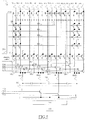
- FIG. 2 and 3 an example of the structure of a portion of the generic memory sector 115 is illustrated, according to an embodiment of the present invention (the elements corresponding to those shown in Figure 1 are denoted with the same reference numerals, and their explanation is omitted for the sake of brevity) .
- Figure 3 is a very simplified cross-sectional view of the structure shown in the Figure 2, along the line III-III. In this section, only some elements of the complete structure are represented.
- the column selection is done in more levels, according to a hierarchical bit line architecture, having two or more hierarchical levels.
- the bit lines are arranged in first-level (or local) bit lines, and second-level bit lines.
- the first-level bit lines are for example formed photolithographically from a first metal layer, whereas the second-level bit lines are formed photolithographically from a second metal layer. Additional hierarchical levels of bit lines can be provided.
- the local bit lines BL1 i can be ideally grouped into two different sets.
- the local bit lines BL1 i belonging to the first set are identified by an index "i" which takes even values (i.e., 0, 2, 7), while the local bit lines BL1 i belonging to the second set are identified by an index "i" which takes odd values (i.e. , 1, 3, ...) .
- the generic local bit line BL1 i belonging to the generic packet P j is selected among the other local bit lines BL1 i belonging to the same packet P j by means of a local selector circuit SP j , corresponding to that packet P j .
- the local selector circuits SP j are each one connected to four command lines. Said command lines (the same for all the local selector circuits SP j belonging to the sector 115) are driven by the column decoder 125c and carry four local decoding signals YL0, YL1, YL2, YL3 provided.
- the generic local selector circuit SP j comprises individual selectors, e.g. pass-transistors M0, M1, M2, M3, for each of the local bit lines BL1 i of the packet, and each of said pass-transistor is controlled by a respective one of the local decoding signals YL0, YL1, YL2, YL3.
- Each global bit line BL2 j is common to more sectors 115, and is selected among the other global bit lines BL2 j by means of a global selector circuit SG, connected to four command lines. Said command lines are driven by the column decoder 125c and carry four global decoding signals YG0, YG1, YG2, YG3.
- eight or even sixteen groups of four packets P j may be provided for.
- FIG. 2 there is also shown a circuit block 200 schematically representing possible higher bit line hierarchical levels, whose presence is however not limitative to the present invention.
- a voltage clamping circuit for holding to ground the ("contour") bit lines adjacent to a selected bit line.
- the voltage clamping circuit includes MOS transistors C 0 , C 1 having a structure identical to the memory cells, but, differently from the memory cells, these transistors C 0 , C 1 (also called “clamping cells”) are not available to the user for storing information.
- the clamping cells are in particular connected to two dedicated clamping control lines CL0, CL1 (similar to the word lines), preferably located in peripheral zones of the memory sector.
- the clamping cells are cells having a properly low threshold voltage value, for example they are unprogrammed cells, adapted to conduct current when activated.
- clamping cells are arranged on the bit lines according to two arrays.
- a first array contains all the clamping cells C 1 connected to the local bit lines BL1 i with even "i" index
- a second array contains all the clamping cells C 0 connected to the local bit lines BL1 i with odd "i" index.
- the clamping cells of the first array are for example located just at the bottom of the memory sector, and are driven by the clamping control line CL1; the clamping cells of the second array are for example located at the top of the memory sector, and are driven by the clamping control line CL0.
- the unused clamping cells (that is, those driven by the clamping control line CL0 but corresponding to an even bit line BL1 i , or those driven by the clamping control line CL1 but corresponding to an odd bit line BL1 i ) are simply lacking of the physical contact with the corresponding local bit line BL1 i .
- the driving of the two clamping control lines CL0, CL1 is managed by a clamping control circuit block 210 (which can be viewed as a part of the column decoder 125c), whose operation will be explained later on.
- V low for example, ground
- the packets P j are formed by four local bit lines BL1 i the individual selector pass-transistors M0, M1, M2, M3 in the local selectors SP j with even index "j" are arranged in such a way that the decoding of the address necessary to the bit line selection associates the first local bit line BL1 i of the generic packet P j with the signal YL0, the second bit line with the signal YL1, the third bit line with the signal YL2 and the last bit line with the signal YL3.
- the individual selector pass-transistors M0, M1, M2, M3 in the local selectors SP j with odd index "j" are arranged in such a way that the first local bit line BL1 i of the generic packet P j is associated with the signal YL3, the second bit line is associated with the signal YL2, the third bit line is associated with the signal YL1 and the last bit line is associated with the signal YL0.
- the clamping control circuit block 210 drives the clamping control lines CL0, CL1 according to the Table 1: Table 1 CLAMPING CONTROL LINE YLh YGj CL0 at V high CL1 at V low Even h Even j Odd h Odd j CL1 at V high CL0 at V low Even h Odd j Odd h Even j
- the column address CADR is divided in column address portions CA1, CA2 (the number of different column address portions, and the number of bits each portion is made up depending on the number of the bit line hierarchical levels).
- This column address portions CA1, CA2 represent the addresses corresponding to each hierarchical level.
- the first (local) level column address portion CA1 is fed to a first-level column decoder 400 (receiving as a supply voltage the memory supply voltage V dd ), that generates the local decoding signals YL0, YL1, YL2, YL3 corresponding to the column address portion CA1, necessary to drive the local selectors SP i .
- the second (local) level column address portion CA2 is fed to a second level column decoder 405 (also receiving as a supply voltage the memory supply voltage V dd ), that generates the global decoding signals YG0, YG1, YG2, YG3 corresponding to the address CA2, necessary to drive the global selector SG.
- the clamping control circuit 210 is supplied by a same supply voltage 408 as the row decoder 125 r .
- the clamping control circuit 210 receives three digital signals b1 b2 (respectively, the least significant bit of the address portion CA1 and the least significant bit of the address portion CA2) and PRG (whose function will be explained later on) at its input, and properly drives the clamping control lines CL0, CL1 for the proper clamping operations.
- FIG. 4B a particular, exemplary and not limitative embodiment of the clamping control circuit 210 is illustrated.
- Three logic XOR gates 310 and a logic NOT gate 308 accomplish the correct logic function that corresponds to that represented by the Table 1.
- clamping cells C 0 and C 1 have an identical structure as the memory cells 110, so the clamping cells may suffer from the typical drawbacks of the others cells (ageing, stress, soft programming and the like). For this reason, the presence of the clamping structures preferably involves some specific precautions.
- the clamping control lines CL0 and CL1 are biased to the same reading voltage as the others word lines WL, and are activated immediately at the start of the reading operation.
- the clamping control lines belonging to the unselected memory sectors 115 remain deactivated.
- the clamping control lines CL0 and CL1 of the selected sector 115 remain respectively activated/deactivated in such a way as to minimize their commutations.
- the selected clamping control line may instead be deactivated after every single reading, to limit the risks of gate-stress on the clamping cells (however, this gate-stress is far less dangerous compared to the gate-stress on memory cells).
- the erasing operation affects the whole memory sector 115, by providing an erasing pulse to all the memory cells 110 belonging to the memory sector 115 selected to be erased.
- all the memory cells 110 belonging to the memory sector 115 are typically pre-programmed, by means of a pre-programming pulse, so as to bring all the cells in a substantially equal starting condition.
- the erasing of the whole memory sector 115 also erases the clamping cells C 0 and C 1 .
- the clamping control circuit 210 addresses only the clamping cells (C 0 or C 1 ) not belonging to the addressed bit line BL1 i .
- the normal operation logic is reversed by setting the pre-programming signal PRG of Figures 4A and 4B to the high logic value.
- the clamping cells C 0 , C 1 are preferably activated.
- the capacitive coupling due to the fringing capacitances Cl between adjacent bit lines BL1 may also cause noise current pulses on the memory cells that are adjacent to the selected cell during the programming phase.
- keeping the clamping control lines deactivated during a programming pulse may be useful to detect the eventually short circuits between bit lines.
Abstract
Description
- The present invention relates to the data storage field; more specifically, the present invention relates to a non-volatile semiconductor memory device.
- Non-volatile memory devices are commonly used to store information which must be preserved also in absence of an electric power source that supply the memory device. A particular class of non-volatile memory devices is electrically programmable, like flash E2PROM. Typically, the memory device includes a matrix of memory cells, for example arranged in rows and columns. Each memory cell consists of a floating gate MOS transistor; the transistor is programmed injecting an electric charge into its floating gate; on the contrary, the transistor is erased removing the electric charge from its floating gate. The electric charge in the floating gate modifies the threshold voltage of the transistor, in such a way as to define different logic values.
- The memory device further includes a bit line for each column of the matrix, and a word line for each matrix row. A typical matrix architecture is the so-called NOR architecture, according to which the generic cell is positioned at the crossing of the bit line and the word line corresponding to the column and row that the cell belongs to, and all the cells of a same column are connected, in parallel to each other and by their drain terminal, to a same bit line.
- A read operation of the memory cells provides for biasing them in prescribed read operating conditions, and detecting the current that the memory cells sink. Particularly, during a reading phase of flash memory cells, it is necessary to bias the addressed bit lines, to which the cells belong, at a reading voltage Vpr, typically 1V.
- The bit lines are conductive lines photolithographically obtained from, e.g., a metal layer. The unavoidable capacitive coupling between selected bit lines (access bit lines) and bit lines adjacent thereto (contour bit lines) causes the generation of a current noise signal on the selected bit lines. This capacitive coupling is due to the fact that, owing to the ultralarge scale of integration, the distance (pitch) between adjacent bit lines in modern memory devices becomes smaller and smaller. Said current noise signal adds up to the reading current of the selected cell during its read operation. During the selected bit line charging (from a starting voltage substantially equal to the ground voltage to the reading voltage Vpr), the adjacent bit lines are capacitively brought towards a voltage value equal to a fraction of the voltage Vpr. Then, the contour bit lines discharge in a way that depends on the programming state of the memory cells adjacent to the accessed memory cell (that is, the memory cells belonging to the same word line as the selected cell, and to the bit lines adjacent to the accessed bit line). In fact, if both of the immediately adjacent cells are programmed (high threshold voltage), and thus do not conduct current, the contour bit lines do not discharge and remain at the voltage value reached during the charging phase. On the contrary, if one of the adjacent cells is not programmed (low threshold voltage), thereby conducting current, the bit line corresponding to the unprogrammed cell discharges toward ground. In short, both, only one, or none of the contour bit lines may discharge toward ground, depending on the state of the adjacent memory cells. Consequently, during the reading phase of a memory cell, a noise current In is superimposed on the cell current Ir, and this noise current In depends on the adjacent memory cells state, so its value can not be forecasted in the design phase. In the case of so-called "multilevel" memory devices, whose memory cells can be programmed in more than two states, the current sunk by each memory cell has more than two possible values, so the noise current is even more variable.
- The total current (I = Ir+In) the sense amplifier receives at its input might determine the detection of a value different from the one actually stored in the accessed cell.
- This problem of bit line capacitive coupling, also referred to as the "fringing" effect problem, results particularly critical when the current difference between different logic values that the cell reading current Ir may take, depending on the logic value stored therein, is small, as for example in the case of multilevel memory devices.
- In view of the state of the art outlined in the foregoing, the Applicant has faced the problem of how to avoid or at least reduce the problem of reading errors caused by fringing effects on the bit lines.
- According to the present invention, a semiconductor memory device as set forth in
claim 1 is provided. - The semiconductor memory device includes a plurality of memory cells, arranged according to a plurality of rows and a plurality of column. The memory devices further includes a plurality of bit lines, each bit line being associated with a respective column of said plurality, and a selecting structure of the bit lines, to select at least one among said bit lines, keeping the remaining bit lines unselected. The memory device further includes a voltage clamping circuit, adapted to causing the clamping at a prescribed voltage of the unselected bit lines adjacent to a selected bit line during an access operation to the memory.
- Further features and advantages of the present invention will be made clear by the following description of a preferred embodiment thereof, given purely by way of a non-restrictive indication, with reference to the attached drawings, wherein:
- Figure 1 schematically shows a memory device in which the present invention can be applied;
- Figure 2 illustrates schematically the structure of a portion of a memory sector of the memory device of Figure 1, according to an embodiment of the present invention;
- Figure 3 illustrates very schematically a cross sectional view along line III-III of Figure 2;
- Figure 4A illustrates a more detailed view of a column decoder of the memory device of Figure 1, according to an embodiment of the present invention;
- Figure 4B illustrates a clamping control circuit according to an embodiment of the present invention; and
- Figure 5 illustrates by way of comparison a particular portion of a memory sector similar to that of Figure 2 but organized with a different bit line decoding.
- With reference to the drawings, in Figure 1 a
non-volatile memory device 100, for example a flash E2PROM, is illustrated. Theflash memory 100 is integrated in a chip of semiconductor material, and includes amatrix 105 ofmemory cells 110; typically, eachcell 110 consists of a floating gate NMOS transistor. In an erased condition, thecell 110 has a low threshold voltage value (conventionally associated with a "1" logic value). Thecell 110 is programmed by injecting electric charges into its floating gate; in the programmed condition, thecell 110 has a high threshold voltage value (conventionally associated with a "0" logic value). Therefore, when aselected cell 110 is biased for reading, thecell 110 is conductive if erased or non-conductive if programmed. In the case of a multilevel flash memory, the electric charge in the floating gate modifies the threshold voltage of the transistor in such a way as to define different logic values, and therefore different conductivity states. For example, in a four-level memory device, the generic memory cell can take one of four different threshold voltage values (associated with the "00", "01", "10" and "11" logic values). - The
matrix 105 is for example organized in a plurality ofmemory sectors 115. - The
cells 110 of the generic memory sector are organized in a plurality of rows (for example, 2048) and a plurality of columns (for example, 4096). To each row there is associated a respective word line WL, while to each column there is associated a respective bit line BL. - The
flash memory 100 has a so-called NOR architecture, in which memory cells of a same column are all connected by their drains in parallel to the bit line corresponding to said column. - The row selection is carried out by means of a
row decoder 125r receiving a row address RADR, decoding it and selecting a corresponding row. Particularly, therow decoder 125r biases the word line WL corresponding to the selected memory cell(s) 110 to a high voltage value (for example, to a value corresponding to a supply voltage Vdd of the memory), while the other word lines are driven to a low voltage value (for example, to the value corresponding to ground). The selection of the matrix column is instead carried out by means of acolumn decoder 125c, receiving a column address CADR and selecting corresponding bit lines BL1 (typically, eight or sixteen bit lines, depending on the memory parallelism) by means of abit line selector 130b, which structure will be analyzed later on. In short, the bit line BL1 corresponding to the addressedmemory cell 110 is selected and connected to asense amplifier 135 by thebit line selector 130b. The other bit lines BL1 (that do not correspond to the addressed memory cell 110) are instead kept isolated from thesense amplifier 135. Thesense amplifier 135 receives memory cell current values corresponding to the state of theselected memory cell 110, and provides an amplified full-logic version thereof, made available at memory output terminals (not shown in Figure 1). - Similar considerations apply if the matrix, and/or the sectors have different sizes, or if the memory cells are implemented with other components. The concepts of the present invention are also applicable when the matrix rows and columns are merely topological definitions, and can be implemented with any other geometrical alignments.
- Considering now Figures 2 and 3, an example of the structure of a portion of the
generic memory sector 115 is illustrated, according to an embodiment of the present invention (the elements corresponding to those shown in Figure 1 are denoted with the same reference numerals, and their explanation is omitted for the sake of brevity) . - More particularly, Figure 3, is a very simplified cross-sectional view of the structure shown in the Figure 2, along the line III-III. In this section, only some elements of the complete structure are represented.
- According to a solution known in the art, the column selection is done in more levels, according to a hierarchical bit line architecture, having two or more hierarchical levels. The bit lines are arranged in first-level (or local) bit lines, and second-level bit lines. The first-level bit lines are for example formed photolithographically from a first metal layer, whereas the second-level bit lines are formed photolithographically from a second metal layer. Additional hierarchical levels of bit lines can be provided.
- According to the example herein considered, in Figure 2 a plurality (sixteen) of local bit lines BL1i (i=0 to 15) is illustrated, the local bit lines consisting of lines photolithographically realized from a first layer of
metal 300, as shown in Figure 3A. The local bit lines BL1i can be ideally grouped into two different sets. The local bit lines BL1i belonging to the first set are identified by an index "i" which takes even values (i.e., 0, 2, ...), while the local bit lines BL1i belonging to the second set are identified by an index "i" which takes odd values (i.e. , 1, 3, ...) . The local bit lines BL1i are also grouped together in packets Pj (j=0 to 3) of, in the example, four bit lines BL1i each. - The generic local bit line BL1i belonging to the generic packet Pj is selected among the other local bit lines BL1i belonging to the same packet Pj by means of a local selector circuit SPj, corresponding to that packet Pj. The local selector circuits SPj are each one connected to four command lines. Said command lines (the same for all the local selector circuits SPj belonging to the sector 115) are driven by the
column decoder 125c and carry four local decoding signals YL0, YL1, YL2, YL3 provided. - The generic local selector circuit SPj comprises individual selectors, e.g. pass-transistors M0, M1, M2, M3, for each of the local bit lines BL1i of the packet, and each of said pass-transistor is controlled by a respective one of the local decoding signals YL0, YL1, YL2, YL3.
- Each packet Pj consisting of four local bit lines BL1i is associated with a corresponding global bit line BL2j (according to this example, j=0 to 3), belonging to the second bit line hierarchical level, and, referring to Figure 3A, consisting of a line photolithographically realized from a
second layer 305 of metal. Each global bit line BL2j is common tomore sectors 115, and is selected among the other global bit lines BL2j by means of a global selector circuit SG, connected to four command lines. Said command lines are driven by thecolumn decoder 125c and carry four global decoding signals YG0, YG1, YG2, YG3. - In a typical memory, eight or even sixteen groups of four packets Pj may be provided for.
- In Figure 2 there is also shown a
circuit block 200 schematically representing possible higher bit line hierarchical levels, whose presence is however not limitative to the present invention. - Fringing field effects between adjacent bit lines exist, as explained in the introduction, which cause capacitive couplings between adjacent bit lines. When a hierarchical bit line architecture is employed, as in the example herein discussed, the fringing effect takes place both at the local bit lines level, and at the level of the global bit lines.
- In Figure 2, the capacitive coupling between adjacent local bit lines BL1i is illustrated by means of "local" fringing capacitances Cl, for simplicity represented as lumped circuit elements; the capacitive coupling between adjacent global bit lines BL2 is represented by means of "global" fringing capacitances Cg. As explained in the introductory part of this description, these capacitive couplings may cause errors during the reading phase.
- To solve the problem, according to an embodiment of the invention, a voltage clamping circuit is provided, for holding to ground the ("contour") bit lines adjacent to a selected bit line. According to an embodiment of the present invention, the voltage clamping circuit includes MOS transistors C0, C1 having a structure identical to the memory cells, but, differently from the memory cells, these transistors C0, C1 (also called "clamping cells") are not available to the user for storing information. The clamping cells are in particular connected to two dedicated clamping control lines CL0, CL1 (similar to the word lines), preferably located in peripheral zones of the memory sector. The clamping cells are cells having a properly low threshold voltage value, for example they are unprogrammed cells, adapted to conduct current when activated. These clamping cells are arranged on the bit lines according to two arrays. A first array contains all the clamping cells C1 connected to the local bit lines BL1i with even "i" index, and a second array contains all the clamping cells C0 connected to the local bit lines BL1i with odd "i" index. The clamping cells of the first array are for example located just at the bottom of the memory sector, and are driven by the clamping control line CL1; the clamping cells of the second array are for example located at the top of the memory sector, and are driven by the clamping control line CL0. The unused clamping cells (that is, those driven by the clamping control line CL0 but corresponding to an even bit line BL1i, or those driven by the clamping control line CL1 but corresponding to an odd bit line BL1i) are simply lacking of the physical contact with the corresponding local bit line BL1i.
- The driving of the two clamping control lines CL0, CL1 is managed by a clamping control circuit block 210 (which can be viewed as a part of the
column decoder 125c), whose operation will be explained later on. - During the reading operation, if the selected cell belongs to an even bit line BL1i (index "i" even), all the clamping cells C0 corresponding to the odd bit lines are activated, by means of a suitable biasing of the corresponding clamping control line CL0. On the contrary, in the case the selected cell belongs to an odd bit line BL1i (index "i" odd), the clamping cells C1 corresponding to the even bit lines are activated, by properly biasing the clamping control line CL1.
- The clamping
control circuit block 210 drives the clamping control lines CL0, CL1 in a complementary, mutually opposite manner, with voltage values Vhigh (for example, Vhigh is equal to a power supply voltage of the memory device Vdd = 3.3V ) and Vlow (for example, ground) . When for example the clamping control line CL0 is driven to the voltage Vhigh by the clampingcontrol circuit block 210, all the clamping cells belonging to the corresponding array are activated, thus all the local bit lines BL1i with odd index "i" are grounded. On the contrary, when the clamping control line CL1 is driven to a voltage Vhigh by the clampingcontrol circuit block 210, all the clamping cells belonging to the corresponding array are activated, thus all the local bit lines BL1i with even index "i" are grounded. - As mentioned previously, the problems due to the fringing effect affects not only the local bit lines, but also the global bit lines BL2j (and the bit lines belonging to the eventual upper hierarchical levels, if present). The exemplary structure shown in Figure 2 allows avoiding the effects of fringing capacitances at the level of the global bit lines as well.
- Referring to Figure 2, wherein, by the way of example, the packets Pj are formed by four local bit lines BL1i the individual selector pass-transistors M0, M1, M2, M3 in the local selectors SPj with even index "j" are arranged in such a way that the decoding of the address necessary to the bit line selection associates the first local bit line BL1i of the generic packet Pj with the signal YL0, the second bit line with the signal YL1, the third bit line with the signal YL2 and the last bit line with the signal YL3.
- On the contrary, the individual selector pass-transistors M0, M1, M2, M3 in the local selectors SPj with odd index "j" are arranged in such a way that the first local bit line BL1i of the generic packet Pj is associated with the signal YL3, the second bit line is associated with the signal YL2, the third bit line is associated with the signal YL1 and the last bit line is associated with the signal YL0.
- Using this particular decoding "scrambling" (YL0-YL1-YL2-YL3, YL3-YL2-YL1-YL0, YL0-YL1-YL2-YL3...) it is possible to automatically clamp both the local bit lines BL1i that are adjacent to the selected local bit line BL1i belonging to the generic packet Pj, and the global bit lines BL2 that are adjacent to the global bit line BL2j corresponding to the packet Pj. To obtain this result, the clamping
control circuit block 210 drives the clamping control lines CL0, CL1 according to the Table 1:Table 1 CLAMPING CONTROL LINE YLh YGj CL0 at Vhigh CL1 at Vlow Even h Even j Odd h Odd j CL1 at Vhigh CL0 at Vlow Even h Odd j Odd h Even j - Referring now to Figure 4A, a more detailed scheme of the
row decoder 125r and thecolumn decoder 125c is illustrated, according to an embodiment of the present invention. The elements corresponding to these shown in Figures 1 or 2 are denoted with the same reference numerals, and their explanation is omitted for the sake of brevity. More particularly, the column address CADR is divided in column address portions CA1, CA2 (the number of different column address portions, and the number of bits each portion is made up depending on the number of the bit line hierarchical levels). This column address portions CA1, CA2 represent the addresses corresponding to each hierarchical level. - According to the particular example represented in Figure 2, the first (local) level column address portion CA1 is fed to a first-level column decoder 400 (receiving as a supply voltage the memory supply voltage Vdd), that generates the local decoding signals YL0, YL1, YL2, YL3 corresponding to the column address portion CA1, necessary to drive the local selectors SPi.
- Similarly, the second (local) level column address portion CA2 is fed to a second level column decoder 405 (also receiving as a supply voltage the memory supply voltage Vdd), that generates the global decoding signals YG0, YG1, YG2, YG3 corresponding to the address CA2, necessary to drive the global selector SG.
- The clamping
control circuit 210 is supplied by asame supply voltage 408 as therow decoder 125r. The clampingcontrol circuit 210 receives three digital signals b1 b2 (respectively, the least significant bit of the address portion CA1 and the least significant bit of the address portion CA2) and PRG (whose function will be explained later on) at its input, and properly drives the clamping control lines CL0, CL1 for the proper clamping operations. - Referring now to Figure 4B, a particular, exemplary and not limitative embodiment of the clamping
control circuit 210 is illustrated. Threelogic XOR gates 310 and alogic NOT gate 308 accomplish the correct logic function that corresponds to that represented by the Table 1. In fact, when the signal PRG is equal to "0" (normal operation), the clamping lines CL0 and CL1 are driven according to the following equations:

- Similar considerations apply if the column selection includes more than two hierarchic levels.
- It is observed that if according to a non preferred embodiment, a different decoding scrambling were adapted (YL0-YL1-YL2-YL3, YL0-YL1-YL2-YL3, YL0-YL1-YL2-YL3...), as shown in Figure 5, the global bit lines adjacent to a selected global bit line would not be automatically clamped as a result of the clamping of the local bit lines BL1i. For clamping also the adjacent global bit lines BL2j it would be necessary to introduce an additional clamping structure.
- It is observed that the clamping cells C0 and C1 have an identical structure as the
memory cells 110, so the clamping cells may suffer from the typical drawbacks of the others cells (ageing, stress, soft programming and the like). For this reason, the presence of the clamping structures preferably involves some specific precautions. - During the reading operation, the clamping control lines CL0 and CL1 are biased to the same reading voltage as the others word lines WL, and are activated immediately at the start of the reading operation. The clamping control lines belonging to the
unselected memory sectors 115 remain deactivated. During a normal sequential access reading operation, in which all thememory cells 110 belonging to a given selected bit line BL1 are read in sequence by means of a sequential activation of the word lines WL of the selectedsector 115, the clamping control lines CL0 and CL1 of the selectedsector 115 remain respectively activated/deactivated in such a way as to minimize their commutations. In the case of a very low-frequency sequential access, the selected clamping control line may instead be deactivated after every single reading, to limit the risks of gate-stress on the clamping cells (however, this gate-stress is far less dangerous compared to the gate-stress on memory cells). - The erasing operation affects the
whole memory sector 115, by providing an erasing pulse to all thememory cells 110 belonging to thememory sector 115 selected to be erased. Before applying the erasing pulse, all thememory cells 110 belonging to thememory sector 115 are typically pre-programmed, by means of a pre-programming pulse, so as to bring all the cells in a substantially equal starting condition. After the erasing operation, it is necessary to verify, by means of a reading phase ("erase verify"), the logic status of thememory cells 110, to ensure that thememory cells 110 are erased. - The erasing of the
whole memory sector 115 also erases the clamping cells C0 and C1. To maintain the same ageing as thememory cells 110, and to avoid that the clamping cells became depleted (negative threshold voltage value), it is necessary to pre-program the clamping cells C0 and C1 too. In order to program the clamping cells, they need to be addressed. Normally, the clampingcontrol circuit 210 addresses only the clamping cells (C0 or C1) not belonging to the addressed bit line BL1i. In order to address the clamping cells for programming them, the normal operation logic is reversed by setting the pre-programming signal PRG of Figures 4A and 4B to the high logic value. In this way, the clamping lines CL0 and CL1 are driven according to the following equations:

- During a programming phase of
normal memory cells 110, the clamping cells C0, C1 are preferably activated. In fact, the capacitive coupling due to the fringing capacitances Cl between adjacent bit lines BL1, in addition to disturbing the memory reading phase, may also cause noise current pulses on the memory cells that are adjacent to the selected cell during the programming phase. However, keeping the clamping control lines deactivated during a programming pulse may be useful to detect the eventually short circuits between bit lines. - Naturally, in order to satisfy local and specific requirements, a person skilled in the art may apply to the solution described above many modifications and alterations all of which, however, are included within the scope of protection of the invention as defined by the following claims.
Claims (11)
- A semiconductor memory device (100), including:a plurality of memory cells (110), arranged according to a plurality of rows and a plurality of columns;a plurality of bit lines (BL1), each bit line being associated with a respective column of said plurality;a selecting structure (130b) of the bit lines, for selecting at least one among said bit lines, keeping the remaining bit lines unselected,characterized by comprising:a voltage clamping circuit (210, CL1, CL0, C1, C0) adapted to causing the clamping at a prescribed voltage of the unselected bit lines adjacent to a selected bit line during an access operation to the memory.
- The memory device (100) of claim 1, wherein said voltage clamping circuit (210, CL1, CL0, C1, C0) includes:a plurality of controlled clamping devices (C1, C0), each one univocally connected to a respective bit line (BL1);a control structure (210) for controlling the controlled clamping devices, by selective activation thereof.
- The memory device (100) of claim 2, wherein:the bit lines (BL1) are grouped in at least a first (BL10, BL12, BL14,..., BL114) and a second (BL11, BL13, BL15,..., BL115) groups, the bit lines belonging to the first group being alternated to the bit lines belonging to the second group;said plurality of controlled clamping devices (C1, C0) is arranged according to at least two arrays, the bit lines belonging to the first group being connected to the controlled clamping devices belonging to the first array, and the bit lines belonging to the second group being connected to the controlled clamping devices belonging to the second array.
- The memory device (100) of claim 3, wherein the control structure (210) for the controlled clamping devices (C1, C0) is adapted to activating the controlled clamping devices belonging to the first array when the selecting structure (130b) of the bit lines selects a bit line (BL11, BL13, BL15,..., BL115) belonging to the second group, and viceversa.
- The memory device (100) of claim 4, wherein the bit lines selecting structure comprises a hierarchic column selecting structure, comprising:a first hierarchic level comprising said bit lines (BL1i) ;a hierarchy of levels higher than the first hierarchic level, said levels hierarchy comprising at least a level higher than the first hierarchic level, said level higher than the first hierarchic level comprising respective higher level bit lines (BL2j) each one associated with a respective packet (Pj) of bit lines belonging to the lower hierarchic level, said packets of bit lines being grouped in at least a first (P0, P2) and a second (P1, P3) collections of packets, the packets belonging to the first collection being alternated to the packets belonging to the second collection; anda plurality of selecting signals (YL0-YL1-YL2-YL3) that are activated in a mutually exclusive manner, said plurality of selecting signals including a number of selecting signals equal to the number of bit lines belonging to the packet;for each packet of bit lines, a respective plurality of selectors (M0, M1, M2, M3), each selector being associated with a respective bit line and being controlled by a respective selecting signal of said plurality, in such a way that the activation of one of said selecting signals determines the selection of a respective bit line of the packet;a correlation between selecting signals and bit lines being such that the generic selecting signal is associated with bit lines belonging to the first group in packets belonging to the first collection, and with bit lines belonging to the second group in packets belonging to the second collection, or with bit lines belonging to the second group in packets belonging to the first collection and with bit lines belonging to the first group in packets belonging to the second collection.
- The memory device (100) of claim 5, wherein the bit lines (BL1i) belonging to the first hierarchic level are formed from a first conductive layer (300), and the bit lines (BL2j) belonging to the level higher than the first (305) are formed from a second conductive layer.
- The memory device (100) of any one of the preceding claims, wherein the controlled clamping devices (C1, C0) include dedicated memory cells of said plurality, that are not available for storing information.
- The memory device (100) of claim 7, in which said dedicated memory cells are arranged in a first and a second alignments each one comprising a number of dedicated cells equal to the number of bit lines (BL1), the dedicated cells belonging to the first alignment being provided with an electric contact to the respective bit lines (BL10, BL12, BL14,..., BL114) of the first group, and the dedicated cells belonging to the second alignment being provided with an electric contact to the respective bit lines (BL11, BL13, BL15,..., BL115) of the second group.
- In a semiconductor memory device including:a plurality of memory cells, arranged in a plurality of rows and a plurality of column, each of said columns having associated a respective bit line;bit lines, each one associated with a respective column of said plurality;a method of selecting the bit lines,characterized by comprising:clamping at a prescribed voltage the unselected bit lines adjacent to a selected bit line during a memory access operation.
- The method of claim 9, wherein the bit lines are grouped in at least a first and a second group, the bit lines belonging to the first group being alternated to the bit lines belonging to the second group,
the method including clamping the bit lines belonging to the group not containing the selected bit lines. - The method of claim 10, wherein the memory device includes a hierarchic column selecting structure comprising:a first hierarchic level comprising said bit lines BL1i;a levels hierarchy of levels higher than the first, said hierarchy comprising at least a level higher than the first, said level higher than the first comprising respective bit lines each associated to a respective packet of bit lines belonging to the lower hierarchic level, said packets of bit lines being grouped in a first and a second collection of packets, the packets belonging to the first collection being alternated to the packets belonging to the second collection,the method further including:clamping bit lines belonging to packets adjacent to the packet containing the selected bit line, wherein said bit lines in the adjacent packets result connected to the corresponding higher-level bit line as a result of the selection of the selected bit line, so as to automatically clamp the bit lines belonging to the level higher than the first adjacent to the bit line belonging to the level higher than the first corresponding to the packet which contains the selected bit line.
Priority Applications (3)
| Application Number | Priority Date | Filing Date | Title |
|---|---|---|---|
| DE602004009078T DE602004009078T2 (en) | 2004-10-15 | 2004-10-15 | memory order |
| EP04105094A EP1647991B1 (en) | 2004-10-15 | 2004-10-15 | A memory device |
| US11/249,763 US7196943B2 (en) | 2004-10-15 | 2005-10-13 | Memory device |
Applications Claiming Priority (1)
| Application Number | Priority Date | Filing Date | Title |
|---|---|---|---|
| EP04105094A EP1647991B1 (en) | 2004-10-15 | 2004-10-15 | A memory device |
Publications (2)
| Publication Number | Publication Date |
|---|---|
| EP1647991A1 true EP1647991A1 (en) | 2006-04-19 |
| EP1647991B1 EP1647991B1 (en) | 2007-09-19 |
Family
ID=34929710
Family Applications (1)
| Application Number | Title | Priority Date | Filing Date |
|---|---|---|---|
| EP04105094A Active EP1647991B1 (en) | 2004-10-15 | 2004-10-15 | A memory device |
Country Status (3)
| Country | Link |
|---|---|
| US (1) | US7196943B2 (en) |
| EP (1) | EP1647991B1 (en) |
| DE (1) | DE602004009078T2 (en) |
Cited By (1)
| Publication number | Priority date | Publication date | Assignee | Title |
|---|---|---|---|---|
| WO2008154359A1 (en) * | 2007-06-07 | 2008-12-18 | Marvell World Trade Ltd. | Electrically alterable non- volatile memory array with embedded logic, and method for arranging |
Families Citing this family (9)
| Publication number | Priority date | Publication date | Assignee | Title |
|---|---|---|---|---|
| DE102004055929B4 (en) * | 2004-11-19 | 2014-05-22 | Qimonda Ag | Non-volatile memory cell arrangement |
| DE602006006029D1 (en) * | 2006-04-12 | 2009-05-14 | St Microelectronics Srl | A column decoding system for semiconductor memory devices implemented with low voltage transistors |
| JP4504397B2 (en) * | 2007-05-29 | 2010-07-14 | 株式会社東芝 | Semiconductor memory device |
| US7733718B2 (en) * | 2007-07-04 | 2010-06-08 | Hynix Semiconductor, Inc. | One-transistor type DRAM |
| US7692975B2 (en) | 2008-05-09 | 2010-04-06 | Micron Technology, Inc. | System and method for mitigating reverse bias leakage |
| US20150071020A1 (en) * | 2013-09-06 | 2015-03-12 | Sony Corporation | Memory device comprising tiles with shared read and write circuits |
| US9349447B1 (en) * | 2015-03-02 | 2016-05-24 | HGST, Inc. | Controlling coupling in large cross-point memory arrays |
| US20160189755A1 (en) * | 2015-08-30 | 2016-06-30 | Chih-Cheng Hsiao | Low power memory device |
| US11087824B2 (en) | 2020-01-10 | 2021-08-10 | Micron Technology, Inc. | Column select swizzle |
Citations (6)
| Publication number | Priority date | Publication date | Assignee | Title |
|---|---|---|---|---|
| US5814853A (en) * | 1996-01-22 | 1998-09-29 | Advanced Micro Devices, Inc. | Sourceless floating gate memory device and method of storing data |
| EP1137011A1 (en) * | 2000-03-21 | 2001-09-26 | STMicroelectronics S.r.l. | String programmable nonvolatile memory with NOR architecture |
| US20030026145A1 (en) * | 2001-02-22 | 2003-02-06 | Yeong-Taek Lee | Bit line setup and discharge circuit for programming non-volatile memory |
| US20030043628A1 (en) * | 2001-08-28 | 2003-03-06 | Samsung Electronics Co., Ltd. | Non-volatile semiconductor memory device with accelerated column scanning scheme |
| US20030161183A1 (en) * | 1999-01-14 | 2003-08-28 | Tran Hieu Van | Digital multilevel non-volatile memory system |
| US20030210581A1 (en) * | 2002-05-09 | 2003-11-13 | Samsung Electronics Co., Ltd. | Low-voltage semiconductor memory device |
Family Cites Families (9)
| Publication number | Priority date | Publication date | Assignee | Title |
|---|---|---|---|---|
| JPH01113999A (en) * | 1987-10-28 | 1989-05-02 | Toshiba Corp | Stress test circuit for non-volatile memory |
| JPH0334198A (en) * | 1989-06-30 | 1991-02-14 | Fujitsu Ltd | Rewritable nonvolatile memory |
| US6240020B1 (en) | 1999-10-25 | 2001-05-29 | Advanced Micro Devices | Method of bitline shielding in conjunction with a precharging scheme for nand-based flash memory devices |
| US6175523B1 (en) | 1999-10-25 | 2001-01-16 | Advanced Micro Devices, Inc | Precharging mechanism and method for NAND-based flash memory devices |
| JP2002100196A (en) | 2000-09-26 | 2002-04-05 | Matsushita Electric Ind Co Ltd | Semiconductor memory |
| KR100399353B1 (en) | 2001-07-13 | 2003-09-26 | 삼성전자주식회사 | Non-volatile semiconductor memory device with time-division sense function and read method thereof |
| KR100465065B1 (en) * | 2002-05-17 | 2005-01-06 | 주식회사 하이닉스반도체 | Clamping circuit and nonvolatile memory device using the same |
| JP3833970B2 (en) | 2002-06-07 | 2006-10-18 | 株式会社東芝 | Nonvolatile semiconductor memory |
| US6717839B1 (en) | 2003-03-31 | 2004-04-06 | Ramtron International Corporation | Bit-line shielding method for ferroelectric memories |
-
2004
- 2004-10-15 DE DE602004009078T patent/DE602004009078T2/en active Active
- 2004-10-15 EP EP04105094A patent/EP1647991B1/en active Active
-
2005
- 2005-10-13 US US11/249,763 patent/US7196943B2/en active Active
Patent Citations (6)
| Publication number | Priority date | Publication date | Assignee | Title |
|---|---|---|---|---|
| US5814853A (en) * | 1996-01-22 | 1998-09-29 | Advanced Micro Devices, Inc. | Sourceless floating gate memory device and method of storing data |
| US20030161183A1 (en) * | 1999-01-14 | 2003-08-28 | Tran Hieu Van | Digital multilevel non-volatile memory system |
| EP1137011A1 (en) * | 2000-03-21 | 2001-09-26 | STMicroelectronics S.r.l. | String programmable nonvolatile memory with NOR architecture |
| US20030026145A1 (en) * | 2001-02-22 | 2003-02-06 | Yeong-Taek Lee | Bit line setup and discharge circuit for programming non-volatile memory |
| US20030043628A1 (en) * | 2001-08-28 | 2003-03-06 | Samsung Electronics Co., Ltd. | Non-volatile semiconductor memory device with accelerated column scanning scheme |
| US20030210581A1 (en) * | 2002-05-09 | 2003-11-13 | Samsung Electronics Co., Ltd. | Low-voltage semiconductor memory device |
Cited By (1)
| Publication number | Priority date | Publication date | Assignee | Title |
|---|---|---|---|---|
| WO2008154359A1 (en) * | 2007-06-07 | 2008-12-18 | Marvell World Trade Ltd. | Electrically alterable non- volatile memory array with embedded logic, and method for arranging |
Also Published As
| Publication number | Publication date |
|---|---|
| DE602004009078T2 (en) | 2008-06-19 |
| US7196943B2 (en) | 2007-03-27 |
| EP1647991B1 (en) | 2007-09-19 |
| DE602004009078D1 (en) | 2007-10-31 |
| US20060083077A1 (en) | 2006-04-20 |
Similar Documents
| Publication | Publication Date | Title |
|---|---|---|
| US7196943B2 (en) | Memory device | |
| KR100935948B1 (en) | Algorithm dynamic reference programming | |
| US7352645B2 (en) | Memory device | |
| KR100897590B1 (en) | Dual-cell soft programming for virtual-ground memory arrays | |
| KR100721295B1 (en) | Nonvolatile memory for storing multibit data | |
| US6807103B2 (en) | Page-erasable flash memory | |
| KR101109458B1 (en) | Non-volatile memory and method with bit line compensation dependent on neighboring operation modes | |
| KR100559716B1 (en) | NAND flash memory device and method of reading the same | |
| US7313023B2 (en) | Partition of non-volatile memory array to reduce bit line capacitance | |
| US6975536B2 (en) | Mass storage array and methods for operation thereof | |
| US5313432A (en) | Segmented, multiple-decoder memory array and method for programming a memory array | |
| US5886924A (en) | Nonvolatile semiconductor memory having sub-arrays formed within pocket wells | |
| US5790456A (en) | Multiple bits-per-cell flash EEPROM memory cells with wide program and erase Vt window | |
| JP7278426B2 (en) | Method of programming memory devices and related memory devices | |
| KR100308480B1 (en) | Flash memory device with row decoding structure which is appropriate for high desitty | |
| US5856942A (en) | Flash memory array and decoding architecture | |
| KR100461486B1 (en) | Non-volatile semiconductor memory device | |
| JP7132443B2 (en) | METHOD OF PROGRAMMING MEMORY DEVICES, SYSTEMS AND RELATED MEMORY DEVICES | |
| JP4439683B2 (en) | Flash memory device having redundancy selection circuit and test method | |
| EP1070323B1 (en) | Page mode erase in a flash memory array | |
| US6714453B2 (en) | Flash memory including means of checking memory cell threshold voltages | |
| US6829173B2 (en) | Semiconductor memory device capable of accurately writing data | |
| EP1214715A1 (en) | 1 transistor cell for eeprom application | |
| KR20040106332A (en) | Refresh scheme for dynamic page programming | |
| US8508993B2 (en) | Method and apparatus of performing an erase operation on a memory integrated circuit |
Legal Events
| Date | Code | Title | Description |
|---|---|---|---|
| PUAI | Public reference made under article 153(3) epc to a published international application that has entered the european phase |
Free format text: ORIGINAL CODE: 0009012 |
|
| AK | Designated contracting states |
Kind code of ref document: A1 Designated state(s): AT BE BG CH CY CZ DE DK EE ES FI FR GB GR HU IE IT LI LU MC NL PL PT RO SE SI SK TR |
|
| AX | Request for extension of the european patent |
Extension state: AL HR LT LV MK |
|
| 17P | Request for examination filed |
Effective date: 20060321 |
|
| AKX | Designation fees paid |
Designated state(s): DE FR GB IT |
|
| GRAP | Despatch of communication of intention to grant a patent |
Free format text: ORIGINAL CODE: EPIDOSNIGR1 |
|
| GRAS | Grant fee paid |
Free format text: ORIGINAL CODE: EPIDOSNIGR3 |
|
| GRAA | (expected) grant |
Free format text: ORIGINAL CODE: 0009210 |
|
| AK | Designated contracting states |
Kind code of ref document: B1 Designated state(s): DE FR GB IT |
|
| REG | Reference to a national code |
Ref country code: GB Ref legal event code: FG4D |
|
| REF | Corresponds to: |
Ref document number: 602004009078 Country of ref document: DE Date of ref document: 20071031 Kind code of ref document: P |
|
| EN | Fr: translation not filed | ||
| PLBE | No opposition filed within time limit |
Free format text: ORIGINAL CODE: 0009261 |
|
| STAA | Information on the status of an ep patent application or granted ep patent |
Free format text: STATUS: NO OPPOSITION FILED WITHIN TIME LIMIT |
|
| 26N | No opposition filed |
Effective date: 20080620 |
|
| PG25 | Lapsed in a contracting state [announced via postgrant information from national office to epo] |
Ref country code: FR Free format text: LAPSE BECAUSE OF FAILURE TO SUBMIT A TRANSLATION OF THE DESCRIPTION OR TO PAY THE FEE WITHIN THE PRESCRIBED TIME-LIMIT Effective date: 20080523 |
|
| PGFP | Annual fee paid to national office [announced via postgrant information from national office to epo] |
Ref country code: GB Payment date: 20080926 Year of fee payment: 5 |
|
| PG25 | Lapsed in a contracting state [announced via postgrant information from national office to epo] |
Ref country code: GB Free format text: LAPSE BECAUSE OF NON-PAYMENT OF DUE FEES Effective date: 20091015 |
|
| PGFP | Annual fee paid to national office [announced via postgrant information from national office to epo] |
Ref country code: IT Payment date: 20071031 Year of fee payment: 4 |
|
| REG | Reference to a national code |
Ref country code: DE Ref legal event code: R082 Ref document number: 602004009078 Country of ref document: DE Representative=s name: KLUNKER, SCHMITT-NILSON, HIRSCH, DE |
|
| REG | Reference to a national code |
Ref country code: DE Ref legal event code: R082 Ref document number: 602004009078 Country of ref document: DE Representative=s name: SCHMITT-NILSON SCHRAUD WAIBEL WOHLFROM PATENTA, DE Effective date: 20131209 Ref country code: DE Ref legal event code: R081 Ref document number: 602004009078 Country of ref document: DE Owner name: MICRON TECHNOLOGY, INC., US Free format text: FORMER OWNER: STMICROELECTRONICS S.R.L., AGRATE BRIANZA, IT Effective date: 20131209 Ref country code: DE Ref legal event code: R082 Ref document number: 602004009078 Country of ref document: DE Representative=s name: KLUNKER, SCHMITT-NILSON, HIRSCH, DE Effective date: 20131209 Ref country code: DE Ref legal event code: R081 Ref document number: 602004009078 Country of ref document: DE Owner name: MICRON TECHNOLOGY, INC., BOISE, US Free format text: FORMER OWNER: STMICROELECTRONICS S.R.L., AGRATE BRIANZA, MAILAND/MILANO, IT Effective date: 20131209 Ref country code: DE Ref legal event code: R081 Ref document number: 602004009078 Country of ref document: DE Owner name: MICRON TECHNOLOGY, INC., BOISE, US Free format text: FORMER OWNER: STMICROELECTRONICS S.R.L., AGRATE BRIANZA, IT Effective date: 20131209 |
|
| REG | Reference to a national code |
Ref country code: DE Ref legal event code: R082 Ref document number: 602004009078 Country of ref document: DE Representative=s name: SCHMITT-NILSON SCHRAUD WAIBEL WOHLFROM PATENTA, DE |
|
| PGFP | Annual fee paid to national office [announced via postgrant information from national office to epo] |
Ref country code: DE Payment date: 20231027 Year of fee payment: 20 |