EP1643559A2 - MOS-gated semiconductor device with top drain - Google Patents
MOS-gated semiconductor device with top drain Download PDFInfo
- Publication number
- EP1643559A2 EP1643559A2 EP05021414A EP05021414A EP1643559A2 EP 1643559 A2 EP1643559 A2 EP 1643559A2 EP 05021414 A EP05021414 A EP 05021414A EP 05021414 A EP05021414 A EP 05021414A EP 1643559 A2 EP1643559 A2 EP 1643559A2
- Authority
- EP
- European Patent Office
- Prior art keywords
- trenches
- substrate
- region
- conductive
- channel
- Prior art date
- Legal status (The legal status is an assumption and is not a legal conclusion. Google has not performed a legal analysis and makes no representation as to the accuracy of the status listed.)
- Withdrawn
Links
Images



Classifications
-
- H—ELECTRICITY
- H10—SEMICONDUCTOR DEVICES; ELECTRIC SOLID-STATE DEVICES NOT OTHERWISE PROVIDED FOR
- H10D—INORGANIC ELECTRIC SEMICONDUCTOR DEVICES
- H10D30/00—Field-effect transistors [FET]
- H10D30/60—Insulated-gate field-effect transistors [IGFET]
- H10D30/64—Double-diffused metal-oxide semiconductor [DMOS] FETs
- H10D30/66—Vertical DMOS [VDMOS] FETs
- H10D30/664—Inverted VDMOS transistors, i.e. source-down VDMOS transistors
-
- H—ELECTRICITY
- H10—SEMICONDUCTOR DEVICES; ELECTRIC SOLID-STATE DEVICES NOT OTHERWISE PROVIDED FOR
- H10D—INORGANIC ELECTRIC SEMICONDUCTOR DEVICES
- H10D30/00—Field-effect transistors [FET]
- H10D30/01—Manufacture or treatment
- H10D30/021—Manufacture or treatment of FETs having insulated gates [IGFET]
- H10D30/028—Manufacture or treatment of FETs having insulated gates [IGFET] of double-diffused metal oxide semiconductor [DMOS] FETs
- H10D30/0291—Manufacture or treatment of FETs having insulated gates [IGFET] of double-diffused metal oxide semiconductor [DMOS] FETs of vertical DMOS [VDMOS] FETs
- H10D30/0297—Manufacture or treatment of FETs having insulated gates [IGFET] of double-diffused metal oxide semiconductor [DMOS] FETs of vertical DMOS [VDMOS] FETs using recessing of the gate electrodes, e.g. to form trench gate electrodes
-
- H—ELECTRICITY
- H10—SEMICONDUCTOR DEVICES; ELECTRIC SOLID-STATE DEVICES NOT OTHERWISE PROVIDED FOR
- H10D—INORGANIC ELECTRIC SEMICONDUCTOR DEVICES
- H10D64/00—Electrodes of devices having potential barriers
- H10D64/20—Electrodes characterised by their shapes, relative sizes or dispositions
- H10D64/23—Electrodes carrying the current to be rectified, amplified, oscillated or switched, e.g. sources, drains, anodes or cathodes
-
- H—ELECTRICITY
- H10—SEMICONDUCTOR DEVICES; ELECTRIC SOLID-STATE DEVICES NOT OTHERWISE PROVIDED FOR
- H10D—INORGANIC ELECTRIC SEMICONDUCTOR DEVICES
- H10D64/00—Electrodes of devices having potential barriers
- H10D64/20—Electrodes characterised by their shapes, relative sizes or dispositions
- H10D64/23—Electrodes carrying the current to be rectified, amplified, oscillated or switched, e.g. sources, drains, anodes or cathodes
- H10D64/251—Source or drain electrodes for field-effect devices
- H10D64/252—Source or drain electrodes for field-effect devices for vertical or pseudo-vertical devices
-
- H—ELECTRICITY
- H10—SEMICONDUCTOR DEVICES; ELECTRIC SOLID-STATE DEVICES NOT OTHERWISE PROVIDED FOR
- H10D—INORGANIC ELECTRIC SEMICONDUCTOR DEVICES
- H10D64/00—Electrodes of devices having potential barriers
- H10D64/20—Electrodes characterised by their shapes, relative sizes or dispositions
- H10D64/27—Electrodes not carrying the current to be rectified, amplified, oscillated or switched, e.g. gates
- H10D64/311—Gate electrodes for field-effect devices
- H10D64/411—Gate electrodes for field-effect devices for FETs
- H10D64/511—Gate electrodes for field-effect devices for FETs for IGFETs
- H10D64/514—Gate electrodes for field-effect devices for FETs for IGFETs characterised by the insulating layers
- H10D64/516—Gate electrodes for field-effect devices for FETs for IGFETs characterised by the insulating layers the thicknesses being non-uniform
Definitions
- This invention is also related to copending application IR-2751 entitled TOP DRAIN MOSGATED DEVICE AND PROCESS OF MANUFACTURE THEREFOR, U.S. Serial No. 11/217.870, filed September 1, 2005 in the names of Daniel M. Kinzer, David Paul Jones and Kyle Spring the subject matter of which is incorporated herein by reference.
- This invention relates to power MOSGATED devices and more specifically to such devices in which the drain is atop the junction-receiving surface of a semiconductor die.
- Power MOSFETs in which the device drain is on top of the junction-receiving surface of the semiconductor die or wafer are well known. Such devices must have a means for shorting the source to body junction which is disposed deeply within the top surface of the die.
- One way of making this junction available has been to form a dedicated trench which extends to the body junction and then forming a conductive short at the trench bottom. This uses die area since it requires a polysilicon gate trench and a separate spaced shorting trench for each cell (or stripe) of the device.
- the source to body short is formed at the bottom of the gate trench, thus permitting a higher density of gate trenches in a trench type power MOSGATED device.
- the shorting material is a conductive silicide at the trench bottom which is a portion of an interrupted silicide layer over the gate polysilicon and drain.
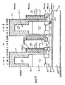
- Figure 1 is a cross-section of a small portion of a trench device in accordance with the invention, showing two adjacent gate trenches in which a silicide coating shorts together the P/P + base (or channel) region and the bottom N/N + source at the bottom of each gate trench.
- Figure 2 shows a small portion of a starting wafer after initial process steps for a second embodiment of the invention and after a trench etch and a TEOS (oxide) deposition.
- Figure 3 shows the structure of Figure 2 after a second trench etch, poly deposition and poly doping, a nitride deposition and a body short implant and drive.
- Figure 4 shows the structure of Figure 3 after a third trench etch and a body short oxide and drive.
- Figure 5 shows the device of Figure 4 after nitride removal; a mesa oxide etch; a source drain implant; a Ti deposition and rapid temperature anneal, and removal of metallic Ti, leaving a titanium silicide layer atop the N + drain contact region and along the polysilicon gate and shorting the N + /P + junction at the bottom of the trench.
- FIG. 1 there is shown, in cross-section, two adjacent "cells", which may be elongated or enclosed in a semiconductor die and constructed in accordance with the invention, and in which the source to body junction is at the bottom of each gate trench.
- the device shown has an N ++ substrate 10 which has a thin N + type layer 11 thereon.
- a P + layer 12 is formed atop layer 11 and a P channel layer 13 is formed atop layer 12.
- An N - drift region 14 is formed atop layer 13 and an N + drain contact layer 15 is formed atop layer 14.
- a conductive silicide layer 16 is disposed atop layer 15 and a front drain metal 17 is disposed atop and in contact with silicide layer 16.
- a back source metal 20 is deposited on the bottom of body 10.
- An N channel device is shown. The conductivity types may be reversed to form a P channel device.
- trenches 30 and 31 Two gate trenches, among a large number of other identical trenches, are formed in the wafer, shown as trenches 30 and 31.
- Trenches 30 and 31 receive insulation oxides such as bottom oxide segments 32 and 33 respectively and are lined with gate oxides 34 and 35 respectively.
- Conductive gate masses 36 and 37 respectively of polysilicon or the like are disposed in trenches 30 and 31 and are operable upon the application of a suitable potential between gates 36 and 37 and drain 17 to invert the channel regions opposite to gate oxides 34 and 35 to turn on the device between top drain 17 and bottom source 20.
- Figures 2 to 5 show a second embodiment of the invention, along with a novel process for the device fabrication.
- the substrate 100 has an N layer 101 on its top and a P + layer 102 is atop layer 101.
- a P channel layer 103 is atop the channel contact layer 102 and an N + type drift region 104 is atop layer 103.
- the thicknesses of the various layers stated above and in Figure 1 are labeled in the right hand margin of the Figures in micrometers, and on the top margin in angstroms.
- an oxide 110 is grown atop the die top surface and a photolithographic step is carried out, ultimately ending in spaced trenches 111 and 112 extending into drift region 104 for a given depth, leaving oxide-covered mesas 113 and 114 in layer 104.
- trenches 120 and 121 there is a further trench etch, forming trenches 120 and 121 and an N type body short implants 122 and 123 are formed in the bottoms of trenches 120 and 121 respectively.
- a gate oxide (450 ⁇ ) 124, 125 is then grown in trenches 120 and 121 respectively, and polysilicon masses 126 and 127 fill trenches 120 and 121 respectively. These masses 126 and 127 are then doped and made conductive and are then etched along their central lengths down to implants 122,123 respectively.
- Nitride layers 131 and 132 are then deposited into trenches 120 and 121 over the exposed walls of polysilicon gate masses 126 and 127. This is followed by a nitride and oxide etch to expose implants 122 and 123. Note that the implants (phosphorus) 122 and 123 can be carried out at this point, if desired, followed by a short drive.
- a further trench etch is carried out, reducing the height of the polysilicon gates 126, 127; and opening windows 140,141 in the bottom of trenches 120 and 121 to the N layer 101.
- the spacer nitride layers 131, 132 are removed and a mesa oxide etch is carried out, removing the oxide 110 down to the level of and coplanar with mesas 113 and 114.
- N + drain implants 150, 151 are then formed in the tops of N drift regions 113 and 114.
- Titanium layers 155 and 156 are then deposited atop the drain implants 150, 151 respectively and, at the same time, titanium contact layers 157 and 158 are deposited at the bottoms of trenches 120 and 121, acting as body shorts in the same trench with the polysilicon gates.
- a rapid thermal anneal process is carried out and excess titanium is stripped, followed by a further rapid thermal anneal.
- trenches 120 and 121 are filled with insulation (not shown); a drain contact (not shown) is formed on the die top and in contact with silicides 155 and 156; and a drain contact (not shown) is deposited on the bottom of substrate 100.
Landscapes
- Electrodes Of Semiconductors (AREA)
- Insulated Gate Type Field-Effect Transistor (AREA)
Abstract
Description
- This application claims the benefit and priority of U.S. Provisional Application No. 60/615,447, filed October 1,2004 the entire disclosure of which is incorporated by reference herein.
- This invention is also related to copending application IR-2751 entitled TOP DRAIN MOSGATED DEVICE AND PROCESS OF MANUFACTURE THEREFOR, U.S. Serial No. 11/217.870, filed September 1, 2005 in the names of Daniel M. Kinzer, David Paul Jones and Kyle Spring the subject matter of which is incorporated herein by reference.
- This invention relates to power MOSGATED devices and more specifically to such devices in which the drain is atop the junction-receiving surface of a semiconductor die.
- Power MOSFETs in which the device drain is on top of the junction-receiving surface of the semiconductor die or wafer are well known. Such devices must have a means for shorting the source to body junction which is disposed deeply within the top surface of the die. One way of making this junction available has been to form a dedicated trench which extends to the body junction and then forming a conductive short at the trench bottom. This uses die area since it requires a polysilicon gate trench and a separate spaced shorting trench for each cell (or stripe) of the device.
- In accordance with the present invention, the source to body short is formed at the bottom of the gate trench, thus permitting a higher density of gate trenches in a trench type power MOSGATED device. Preferably, the shorting material is a conductive silicide at the trench bottom which is a portion of an interrupted silicide layer over the gate polysilicon and drain.
- Figure 1 is a cross-section of a small portion of a trench device in accordance with the invention, showing two adjacent gate trenches in which a silicide coating shorts together the P/P+ base (or channel) region and the bottom N/N+ source at the bottom of each gate trench.
- Figure 2 shows a small portion of a starting wafer after initial process steps for a second embodiment of the invention and after a trench etch and a TEOS (oxide) deposition..
- Figure 3 shows the structure of Figure 2 after a second trench etch, poly deposition and poly doping, a nitride deposition and a body short implant and drive.
- Figure 4 shows the structure of Figure 3 after a third trench etch and a body short oxide and drive.
- Figure 5 shows the device of Figure 4 after nitride removal; a mesa oxide etch; a source drain implant; a Ti deposition and rapid temperature anneal, and removal of metallic Ti, leaving a titanium silicide layer atop the N+ drain contact region and along the polysilicon gate and shorting the N+/P+ junction at the bottom of the trench.
- Referring first to Figure 1, there is shown, in cross-section, two adjacent "cells", which may be elongated or enclosed in a semiconductor die and constructed in accordance with the invention, and in which the source to body junction is at the bottom of each gate trench.
- Thus, in Figure 1, the device shown has an N++ substrate 10 which has a thin N+ type layer 11 thereon. A P+
layer 12 is formed atop layer 11 and a P channel layer 13 is formed atoplayer 12. An N- drift region 14 is formed atop layer 13 and an N+ drain contact layer 15 is formed atop layer 14. A conductive silicide layer 16 is disposed atop layer 15 and afront drain metal 17 is disposed atop and in contact with silicide layer 16. Note that aback source metal 20 is deposited on the bottom of body 10. An N channel device is shown. The conductivity types may be reversed to form a P channel device. - Two gate trenches, among a large number of other identical trenches, are formed in the wafer, shown as
trenches bottom oxide segments gate oxides Conductive gate masses 36 and 37 respectively of polysilicon or the like are disposed intrenches gates 36 and 37 anddrain 17 to invert the channel regions opposite togate oxides top drain 17 andbottom source 20. - Note that all
gates 36, 37 are suitably connected together in any desired manner (not shown). Note further that thetrenches poly masses 36 and 37 by oxide fillers and caps 40 and 41. - It is necessary to short circuit the parasitic N/P/N transistor formed by N region 14; P region 13; and N region 10 to prevent the turn on of this bipolar device. In accordance with the invention, this short is provided at the bottom of each
trench trenches - This short is improved by the provision of N+ and
N contact regions 60 and 61 respectively. - Figures 2 to 5 show a second embodiment of the invention, along with a novel process for the device fabrication.
- Referring first to Figure 2, there is shown the starting N++ substrate 100 with initial process steps. Like the embodiment of Figure 1, the
substrate 100 has anN layer 101 on its top and a P+ layer 102 is atoplayer 101. A Pchannel layer 103 is atop thechannel contact layer 102 and an N+type drift region 104 is atoplayer 103. The thicknesses of the various layers stated above and in Figure 1 are labeled in the right hand margin of the Figures in micrometers, and on the top margin in angstroms. - As a first major step in the sequence to prepare the wafer, and as shown in Figure 2, an
oxide 110 is grown atop the die top surface and a photolithographic step is carried out, ultimately ending inspaced trenches 111 and 112 extending intodrift region 104 for a given depth, leaving oxide-coveredmesas layer 104. - Thereafter, and as shown in Figure 3, there is a further trench etch, forming
trenches short implants trenches - A gate oxide (450Å) 124, 125 is then grown in
trenches polysilicon masses fill trenches masses - Nitride
layers 131 and 132 (150Å) are then deposited intotrenches polysilicon gate masses implants - Turning next to Figure 4, a further trench etch is carried out, reducing the height of the
polysilicon gates trenches N layer 101. - Thereafter, and as shown in Figure 5, the
spacer nitride layers oxide 110 down to the level of and coplanar withmesas N drift regions - Titanium layers 155 and 156 are then deposited atop the
drain implants titanium contact layers 157 and 158 are deposited at the bottoms oftrenches - Thereafter,
trenches substrate 100. - Although the present invention has been described in relation to particular embodiments thereof, many other variations and modifications and other uses will become apparent to those skilled in the art. It is preferred, therefore, that the present invention be limited not by the specific disclosure herein.
Claims (15)
- A top drain MOSgated device, comprising, in combination, a semiconductor die having a top and bottom surface, a substrate of one conductivity type extending from said bottom surface, a channel region of a second conductivity type atop said substrate and a drift region of said one conductivity type atop said channel region; a plurality of parallel spaced trenches extending from said top surface, and through said drift region, said channel region and terminating in said substrate region; the bottom of each of said trenches having respective conductive layers connecting said substrate region to said channel region; a bottom insulating mass in the bottom of each of said trenches; a gate oxide lining the walls of each of said trenches adjacent at least a portion of the depth of said channel region; a conductive gate mass within each of said trenches and bounded on their bottoms by said bottom insulating mass and at their sides by said gate oxide liners; a top insulation mass substantially filling the tops of said trenches above the tops of said conductive gate masses; and a top drain electrode disposed on said top surface and in contact with said drift region between said trenches; and a bottom source electrode connected to said bottom surface,
- The device of claim 1, wherein said one conductivity is the N type.
- The device of claim 1, wherein said conductive mass is conductive polysilicon.
- The device of claim 1, wherein said conductive layers on the bottom of said trenches is of a conductive silicide.
- The device of claim 1, which further includes a contact diffusion of increased concentration of carriers of said one type atop said drift region layer.
- The device of claim 1, which further includes a conductive silicide layer atop said drift region.
- The device of claim 1, which further includes a diffusion of said second conductivity type and of greater concentration than that of said channel layer disposed between said channel layer and said substrate.
- The device of claim 1, which further includes a contact diffusion of said one type formed on the walls of said trenches and extending from said channel region to said substrate and contacting the exterior side walls of said conductive layers.
- The device of claim 4, which further includes a contact diffusion of increased concentration of carriers of said one type atop said drift region layer.
- The device of claim 4, which further includes a conductive silicide layer atop said drift region.
- The device of claim 9, which further includes a conductive silicide layer atop said drift region.
- The device of claim 10, which further includes a diffusion of said second conductivity type and of greater concentration than that of said channel layer disposed between said channel layer and said substrate.
- The device of claim 11, which further includes a diffusion of said second conductivity type and of greater concentration than that of said channel layer disposed between said channel layer and said substrate.
- The device of claim 13, which further includes a contact diffusion of said one type formed on the walls of said trenches and extending from said channel region to said substrate and contacting the exterior side walls of said conductive layers.
- The device of claim 10, wherein said conductive silicide layers are applied in a single deposition step.
Applications Claiming Priority (2)
| Application Number | Priority Date | Filing Date | Title |
|---|---|---|---|
| US61544704P | 2004-10-01 | 2004-10-01 | |
| US11/238,207 US7456470B2 (en) | 2004-10-01 | 2005-09-29 | Top drain fet with integrated body short |
Publications (2)
| Publication Number | Publication Date |
|---|---|
| EP1643559A2 true EP1643559A2 (en) | 2006-04-05 |
| EP1643559A3 EP1643559A3 (en) | 2007-11-07 |
Family
ID=35455871
Family Applications (1)
| Application Number | Title | Priority Date | Filing Date |
|---|---|---|---|
| EP05021414A Withdrawn EP1643559A3 (en) | 2004-10-01 | 2005-09-30 | MOS-gated semiconductor device with top drain |
Country Status (3)
| Country | Link |
|---|---|
| US (1) | US7456470B2 (en) |
| EP (1) | EP1643559A3 (en) |
| JP (1) | JP2006310735A (en) |
Families Citing this family (19)
| Publication number | Priority date | Publication date | Assignee | Title |
|---|---|---|---|---|
| US7648869B2 (en) * | 2006-01-12 | 2010-01-19 | International Business Machines Corporation | Method of fabricating semiconductor structures for latch-up suppression |
| US20070158779A1 (en) * | 2006-01-12 | 2007-07-12 | International Business Machines Corporation | Methods and semiconductor structures for latch-up suppression using a buried damage layer |
| US7276768B2 (en) * | 2006-01-26 | 2007-10-02 | International Business Machines Corporation | Semiconductor structures for latch-up suppression and methods of forming such semiconductor structures |
| US7491618B2 (en) * | 2006-01-26 | 2009-02-17 | International Business Machines Corporation | Methods and semiconductor structures for latch-up suppression using a conductive region |
| US20070194403A1 (en) * | 2006-02-23 | 2007-08-23 | International Business Machines Corporation | Methods for fabricating semiconductor device structures with reduced susceptibility to latch-up and semiconductor device structures formed by the methods |
| US7982284B2 (en) * | 2006-06-28 | 2011-07-19 | Infineon Technologies Ag | Semiconductor component including an isolation structure and a contact to the substrate |
| DE102006029701B4 (en) * | 2006-06-28 | 2017-06-01 | Infineon Technologies Ag | Semiconductor component and method for producing a semiconductor device |
| US7633120B2 (en) * | 2006-08-08 | 2009-12-15 | Alph & Omega Semiconductor, Ltd. | Inverted-trench grounded-source field effect transistor (FET) structure using highly conductive substrates |
| US7818702B2 (en) * | 2007-02-28 | 2010-10-19 | International Business Machines Corporation | Structure incorporating latch-up resistant semiconductor device structures on hybrid substrates |
| US7754513B2 (en) * | 2007-02-28 | 2010-07-13 | International Business Machines Corporation | Latch-up resistant semiconductor structures on hybrid substrates and methods for forming such semiconductor structures |
| US7989885B2 (en) * | 2009-02-26 | 2011-08-02 | Infineon Technologies Austria Ag | Semiconductor device having means for diverting short circuit current arranged in trench and method for producing same |
| US10205017B2 (en) * | 2009-06-17 | 2019-02-12 | Alpha And Omega Semiconductor Incorporated | Bottom source NMOS triggered Zener clamp for configuring an ultra-low voltage transient voltage suppressor (TVS) |
| DE102010039258B4 (en) * | 2010-08-12 | 2018-03-15 | Infineon Technologies Austria Ag | Transistor device with reduced short-circuit current |
| WO2012158977A2 (en) | 2011-05-18 | 2012-11-22 | Vishay-Siliconix | Semiconductor device |
| US8471331B2 (en) * | 2011-08-15 | 2013-06-25 | Semiconductor Components Industries, Llc | Method of making an insulated gate semiconductor device with source-substrate connection and structure |
| US8723238B1 (en) | 2013-03-15 | 2014-05-13 | Semiconductor Components Industries, Llc | Method of forming a transistor and structure therefor |
| US9466708B2 (en) | 2013-03-15 | 2016-10-11 | Semiconductor Components Industries, Llc | Method of forming a transistor and structure therefor |
| US9397159B2 (en) | 2014-09-12 | 2016-07-19 | Taiwan Semiconductor Manufacturing Company, Ltd. | Silicide region of gate-all-around transistor |
| US11869967B2 (en) | 2021-08-12 | 2024-01-09 | Alpha And Omega Semiconductor International Lp | Bottom source trench MOSFET with shield electrode |
Family Cites Families (8)
| Publication number | Priority date | Publication date | Assignee | Title |
|---|---|---|---|---|
| JPS63288068A (en) * | 1987-05-20 | 1988-11-25 | Sanyo Electric Co Ltd | Semiconductor device |
| US5023196A (en) * | 1990-01-29 | 1991-06-11 | Motorola Inc. | Method for forming a MOSFET with substrate source contact |
| US5134448A (en) * | 1990-01-29 | 1992-07-28 | Motorola, Inc. | MOSFET with substrate source contact |
| GB9916868D0 (en) * | 1999-07-20 | 1999-09-22 | Koninkl Philips Electronics Nv | Trench-gate field-effect transistors and their manufacture |
| DE10004984A1 (en) * | 2000-02-04 | 2001-08-16 | Infineon Technologies Ag | Vertical semiconductor device with source-down design and corresponding manufacturing process |
| JP2003051598A (en) * | 2001-05-31 | 2003-02-21 | Hideshi Ito | High frequency power MOSFET |
| AU2003279478A1 (en) * | 2002-12-19 | 2004-07-14 | Koninklijke Philips Electronics N.V. | Non-volatile memory cell and method of fabrication |
| US6906380B1 (en) * | 2004-05-13 | 2005-06-14 | Vishay-Siliconix | Drain side gate trench metal-oxide-semiconductor field effect transistor |
-
2005
- 2005-09-29 US US11/238,207 patent/US7456470B2/en not_active Expired - Lifetime
- 2005-09-30 EP EP05021414A patent/EP1643559A3/en not_active Withdrawn
- 2005-10-03 JP JP2005289980A patent/JP2006310735A/en not_active Ceased
Also Published As
| Publication number | Publication date |
|---|---|
| US20060113589A1 (en) | 2006-06-01 |
| US7456470B2 (en) | 2008-11-25 |
| JP2006310735A (en) | 2006-11-09 |
| EP1643559A3 (en) | 2007-11-07 |
Similar Documents
| Publication | Publication Date | Title |
|---|---|---|
| US7456470B2 (en) | Top drain fet with integrated body short | |
| US6987305B2 (en) | Integrated FET and schottky device | |
| US10355125B2 (en) | Electrode contact structure for semiconductor device | |
| JP3728073B2 (en) | Semiconductor device controllable by electric field effect and manufacturing method thereof | |
| US6144065A (en) | MOS gated device with self aligned cells | |
| JP3365984B2 (en) | MOS gate device and its manufacturing process | |
| US6319777B1 (en) | Trench semiconductor device manufacture with a thicker upper insulating layer | |
| US6798016B2 (en) | Trench MOS device and process for radhard device | |
| US6846706B2 (en) | Power MOSFET with ultra-deep base and reduced on resistance | |
| US9837358B2 (en) | Source-gate region architecture in a vertical power semiconductor device | |
| US20070034911A1 (en) | Metal-oxide-semiconductor transistor and method of manufacturing the same | |
| US7285823B2 (en) | Superjunction semiconductor device structure | |
| US6509608B1 (en) | Trench-gate field-effect transistors and their manufacture | |
| WO2009154882A2 (en) | Semiconductor power switches having trench gates | |
| JP2003533050A (en) | Semiconductor device | |
| US6838735B1 (en) | Trench FET with non overlapping poly and remote contact therefor | |
| EP1162665A2 (en) | Trench gate MIS device and method of fabricating the same | |
| US7494876B1 (en) | Trench-gated MIS device having thick polysilicon insulation layer at trench bottom and method of fabricating the same | |
| US20070132016A1 (en) | Trench ld structure |
Legal Events
| Date | Code | Title | Description |
|---|---|---|---|
| PUAI | Public reference made under article 153(3) epc to a published international application that has entered the european phase |
Free format text: ORIGINAL CODE: 0009012 |
|
| AK | Designated contracting states |
Kind code of ref document: A2 Designated state(s): AT BE BG CH CY CZ DE DK EE ES FI FR GB GR HU IE IS IT LI LT LU LV MC NL PL PT RO SE SI SK TR |
|
| AX | Request for extension of the european patent |
Extension state: AL BA HR MK YU |
|
| PUAL | Search report despatched |
Free format text: ORIGINAL CODE: 0009013 |
|
| AK | Designated contracting states |
Kind code of ref document: A3 Designated state(s): AT BE BG CH CY CZ DE DK EE ES FI FR GB GR HU IE IS IT LI LT LU LV MC NL PL PT RO SE SI SK TR |
|
| AX | Request for extension of the european patent |
Extension state: AL BA HR MK YU |
|
| RIC1 | Information provided on ipc code assigned before grant |
Ipc: H01L 29/423 20060101ALN20071001BHEP Ipc: H01L 29/417 20060101ALN20071001BHEP Ipc: H01L 21/336 20060101ALI20071001BHEP Ipc: H01L 29/78 20060101AFI20051228BHEP |
|
| AKX | Designation fees paid | ||
| STAA | Information on the status of an ep patent application or granted ep patent |
Free format text: STATUS: THE APPLICATION IS DEEMED TO BE WITHDRAWN |
|
| REG | Reference to a national code |
Ref country code: DE Ref legal event code: 8566 |
|
| 18D | Application deemed to be withdrawn |
Effective date: 20080401 |