EP1643294A2 - Refractive index changing apparatus and method - Google Patents
Refractive index changing apparatus and method Download PDFInfo
- Publication number
- EP1643294A2 EP1643294A2 EP05256064A EP05256064A EP1643294A2 EP 1643294 A2 EP1643294 A2 EP 1643294A2 EP 05256064 A EP05256064 A EP 05256064A EP 05256064 A EP05256064 A EP 05256064A EP 1643294 A2 EP1643294 A2 EP 1643294A2
- Authority
- EP
- European Patent Office
- Prior art keywords
- energy
- level
- quantum dots
- refractive index
- ground level
- Prior art date
- Legal status (The legal status is an assumption and is not a legal conclusion. Google has not performed a legal analysis and makes no representation as to the accuracy of the status listed.)
- Withdrawn
Links
- 238000000034 method Methods 0.000 title claims description 17
- 239000002096 quantum dot Substances 0.000 claims abstract description 126
- 238000002347 injection Methods 0.000 claims abstract description 65
- 239000007924 injection Substances 0.000 claims abstract description 65
- 230000004888 barrier function Effects 0.000 claims abstract description 53
- 230000005641 tunneling Effects 0.000 claims abstract description 28
- 230000000694 effects Effects 0.000 claims abstract description 18
- 239000004065 semiconductor Substances 0.000 claims description 7
- 239000010419 fine particle Substances 0.000 claims description 6
- OKTJSMMVPCPJKN-UHFFFAOYSA-N Carbon Chemical compound [C] OKTJSMMVPCPJKN-UHFFFAOYSA-N 0.000 claims description 4
- 239000002041 carbon nanotube Substances 0.000 claims description 4
- 229910021393 carbon nanotube Inorganic materials 0.000 claims description 4
- 230000005281 excited state Effects 0.000 claims description 4
- 229910052751 metal Inorganic materials 0.000 claims description 4
- 239000002184 metal Substances 0.000 claims description 4
- XMWRBQBLMFGWIX-UHFFFAOYSA-N C60 fullerene Chemical compound C12=C3C(C4=C56)=C7C8=C5C5=C9C%10=C6C6=C4C1=C1C4=C6C6=C%10C%10=C9C9=C%11C5=C8C5=C8C7=C3C3=C7C2=C1C1=C2C4=C6C4=C%10C6=C9C9=C%11C5=C5C8=C3C3=C7C1=C1C2=C4C6=C2C9=C5C3=C12 XMWRBQBLMFGWIX-UHFFFAOYSA-N 0.000 claims description 3
- 229910003472 fullerene Inorganic materials 0.000 claims description 3
- 238000005315 distribution function Methods 0.000 claims description 2
- 230000005283 ground state Effects 0.000 claims description 2
- 230000008859 change Effects 0.000 description 41
- 230000003287 optical effect Effects 0.000 description 17
- 239000000463 material Substances 0.000 description 15
- 239000004793 Polystyrene Substances 0.000 description 10
- 229920002223 polystyrene Polymers 0.000 description 10
- 239000003990 capacitor Substances 0.000 description 7
- 230000005684 electric field Effects 0.000 description 7
- 238000004770 highest occupied molecular orbital Methods 0.000 description 7
- 230000005284 excitation Effects 0.000 description 6
- 238000004768 lowest unoccupied molecular orbital Methods 0.000 description 6
- 239000004973 liquid crystal related substance Substances 0.000 description 5
- 230000005697 Pockels effect Effects 0.000 description 3
- 238000010521 absorption reaction Methods 0.000 description 3
- 238000000862 absorption spectrum Methods 0.000 description 3
- 230000008901 benefit Effects 0.000 description 3
- 230000005540 biological transmission Effects 0.000 description 2
- UHYPYGJEEGLRJD-UHFFFAOYSA-N cadmium(2+);selenium(2-) Chemical compound [Se-2].[Cd+2] UHYPYGJEEGLRJD-UHFFFAOYSA-N 0.000 description 2
- 239000011521 glass Substances 0.000 description 2
- 229910052737 gold Inorganic materials 0.000 description 2
- 239000010931 gold Substances 0.000 description 2
- 239000002105 nanoparticle Substances 0.000 description 2
- 229910004613 CdTe Inorganic materials 0.000 description 1
- 229910001218 Gallium arsenide Inorganic materials 0.000 description 1
- 229910000673 Indium arsenide Inorganic materials 0.000 description 1
- 230000005374 Kerr effect Effects 0.000 description 1
- 229910007709 ZnTe Inorganic materials 0.000 description 1
- 230000000903 blocking effect Effects 0.000 description 1
- 229910052792 caesium Inorganic materials 0.000 description 1
- TVFDJXOCXUVLDH-UHFFFAOYSA-N caesium atom Chemical compound [Cs] TVFDJXOCXUVLDH-UHFFFAOYSA-N 0.000 description 1
- 229910052802 copper Inorganic materials 0.000 description 1
- 230000001687 destabilization Effects 0.000 description 1
- 238000011161 development Methods 0.000 description 1
- 229910003460 diamond Inorganic materials 0.000 description 1
- 239000010432 diamond Substances 0.000 description 1
- 230000005672 electromagnetic field Effects 0.000 description 1
- 230000007613 environmental effect Effects 0.000 description 1
- 229910052732 germanium Inorganic materials 0.000 description 1
- PCHJSUWPFVWCPO-UHFFFAOYSA-N gold Chemical compound [Au] PCHJSUWPFVWCPO-UHFFFAOYSA-N 0.000 description 1
- WPYVAWXEWQSOGY-UHFFFAOYSA-N indium antimonide Chemical compound [Sb]#[In] WPYVAWXEWQSOGY-UHFFFAOYSA-N 0.000 description 1
- RPQDHPTXJYYUPQ-UHFFFAOYSA-N indium arsenide Chemical compound [In]#[As] RPQDHPTXJYYUPQ-UHFFFAOYSA-N 0.000 description 1
- AMGQUBHHOARCQH-UHFFFAOYSA-N indium;oxotin Chemical compound [In].[Sn]=O AMGQUBHHOARCQH-UHFFFAOYSA-N 0.000 description 1
- 230000001939 inductive effect Effects 0.000 description 1
- 230000003993 interaction Effects 0.000 description 1
- 229910052742 iron Inorganic materials 0.000 description 1
- 230000001678 irradiating effect Effects 0.000 description 1
- 229910052745 lead Inorganic materials 0.000 description 1
- 239000007788 liquid Substances 0.000 description 1
- 230000007246 mechanism Effects 0.000 description 1
- 239000002082 metal nanoparticle Substances 0.000 description 1
- 150000002739 metals Chemical class 0.000 description 1
- 238000004776 molecular orbital Methods 0.000 description 1
- 239000002159 nanocrystal Substances 0.000 description 1
- 229920000642 polymer Polymers 0.000 description 1
- 230000008569 process Effects 0.000 description 1
- 238000001454 recorded image Methods 0.000 description 1
- 238000011160 research Methods 0.000 description 1
- 238000012827 research and development Methods 0.000 description 1
- 239000000523 sample Substances 0.000 description 1
- SBIBMFFZSBJNJF-UHFFFAOYSA-N selenium;zinc Chemical compound [Se]=[Zn] SBIBMFFZSBJNJF-UHFFFAOYSA-N 0.000 description 1
- 229910052710 silicon Inorganic materials 0.000 description 1
- 229910052709 silver Inorganic materials 0.000 description 1
- 239000000126 substance Substances 0.000 description 1
- 229910052718 tin Inorganic materials 0.000 description 1
- 238000002834 transmittance Methods 0.000 description 1
- 230000005428 wave function Effects 0.000 description 1
Images
Classifications
-
- G—PHYSICS
- G02—OPTICS
- G02F—OPTICAL DEVICES OR ARRANGEMENTS FOR THE CONTROL OF LIGHT BY MODIFICATION OF THE OPTICAL PROPERTIES OF THE MEDIA OF THE ELEMENTS INVOLVED THEREIN; NON-LINEAR OPTICS; FREQUENCY-CHANGING OF LIGHT; OPTICAL LOGIC ELEMENTS; OPTICAL ANALOGUE/DIGITAL CONVERTERS
- G02F1/00—Devices or arrangements for the control of the intensity, colour, phase, polarisation or direction of light arriving from an independent light source, e.g. switching, gating or modulating; Non-linear optics
- G02F1/01—Devices or arrangements for the control of the intensity, colour, phase, polarisation or direction of light arriving from an independent light source, e.g. switching, gating or modulating; Non-linear optics for the control of the intensity, phase, polarisation or colour
- G02F1/015—Devices or arrangements for the control of the intensity, colour, phase, polarisation or direction of light arriving from an independent light source, e.g. switching, gating or modulating; Non-linear optics for the control of the intensity, phase, polarisation or colour based on semiconductor elements having potential barriers, e.g. having a PN or PIN junction
- G02F1/017—Structures with periodic or quasi periodic potential variation, e.g. superlattices, quantum wells
- G02F1/01716—Optically controlled superlattice or quantum well devices
-
- B—PERFORMING OPERATIONS; TRANSPORTING
- B82—NANOTECHNOLOGY
- B82Y—SPECIFIC USES OR APPLICATIONS OF NANOSTRUCTURES; MEASUREMENT OR ANALYSIS OF NANOSTRUCTURES; MANUFACTURE OR TREATMENT OF NANOSTRUCTURES
- B82Y20/00—Nanooptics, e.g. quantum optics or photonic crystals
-
- G—PHYSICS
- G02—OPTICS
- G02F—OPTICAL DEVICES OR ARRANGEMENTS FOR THE CONTROL OF LIGHT BY MODIFICATION OF THE OPTICAL PROPERTIES OF THE MEDIA OF THE ELEMENTS INVOLVED THEREIN; NON-LINEAR OPTICS; FREQUENCY-CHANGING OF LIGHT; OPTICAL LOGIC ELEMENTS; OPTICAL ANALOGUE/DIGITAL CONVERTERS
- G02F1/00—Devices or arrangements for the control of the intensity, colour, phase, polarisation or direction of light arriving from an independent light source, e.g. switching, gating or modulating; Non-linear optics
- G02F1/01—Devices or arrangements for the control of the intensity, colour, phase, polarisation or direction of light arriving from an independent light source, e.g. switching, gating or modulating; Non-linear optics for the control of the intensity, phase, polarisation or colour
- G02F1/015—Devices or arrangements for the control of the intensity, colour, phase, polarisation or direction of light arriving from an independent light source, e.g. switching, gating or modulating; Non-linear optics for the control of the intensity, phase, polarisation or colour based on semiconductor elements having potential barriers, e.g. having a PN or PIN junction
- G02F1/0151—Devices or arrangements for the control of the intensity, colour, phase, polarisation or direction of light arriving from an independent light source, e.g. switching, gating or modulating; Non-linear optics for the control of the intensity, phase, polarisation or colour based on semiconductor elements having potential barriers, e.g. having a PN or PIN junction modulating the refractive index
-
- G—PHYSICS
- G02—OPTICS
- G02F—OPTICAL DEVICES OR ARRANGEMENTS FOR THE CONTROL OF LIGHT BY MODIFICATION OF THE OPTICAL PROPERTIES OF THE MEDIA OF THE ELEMENTS INVOLVED THEREIN; NON-LINEAR OPTICS; FREQUENCY-CHANGING OF LIGHT; OPTICAL LOGIC ELEMENTS; OPTICAL ANALOGUE/DIGITAL CONVERTERS
- G02F1/00—Devices or arrangements for the control of the intensity, colour, phase, polarisation or direction of light arriving from an independent light source, e.g. switching, gating or modulating; Non-linear optics
- G02F1/01—Devices or arrangements for the control of the intensity, colour, phase, polarisation or direction of light arriving from an independent light source, e.g. switching, gating or modulating; Non-linear optics for the control of the intensity, phase, polarisation or colour
- G02F1/015—Devices or arrangements for the control of the intensity, colour, phase, polarisation or direction of light arriving from an independent light source, e.g. switching, gating or modulating; Non-linear optics for the control of the intensity, phase, polarisation or colour based on semiconductor elements having potential barriers, e.g. having a PN or PIN junction
- G02F1/017—Structures with periodic or quasi periodic potential variation, e.g. superlattices, quantum wells
- G02F1/01791—Quantum boxes or quantum dots
-
- G—PHYSICS
- G02—OPTICS
- G02F—OPTICAL DEVICES OR ARRANGEMENTS FOR THE CONTROL OF LIGHT BY MODIFICATION OF THE OPTICAL PROPERTIES OF THE MEDIA OF THE ELEMENTS INVOLVED THEREIN; NON-LINEAR OPTICS; FREQUENCY-CHANGING OF LIGHT; OPTICAL LOGIC ELEMENTS; OPTICAL ANALOGUE/DIGITAL CONVERTERS
- G02F2203/00—Function characteristic
- G02F2203/50—Phase-only modulation
-
- Y—GENERAL TAGGING OF NEW TECHNOLOGICAL DEVELOPMENTS; GENERAL TAGGING OF CROSS-SECTIONAL TECHNOLOGIES SPANNING OVER SEVERAL SECTIONS OF THE IPC; TECHNICAL SUBJECTS COVERED BY FORMER USPC CROSS-REFERENCE ART COLLECTIONS [XRACs] AND DIGESTS
- Y10—TECHNICAL SUBJECTS COVERED BY FORMER USPC
- Y10S—TECHNICAL SUBJECTS COVERED BY FORMER USPC CROSS-REFERENCE ART COLLECTIONS [XRACs] AND DIGESTS
- Y10S977/00—Nanotechnology
- Y10S977/70—Nanostructure
- Y10S977/773—Nanoparticle, i.e. structure having three dimensions of 100 nm or less
- Y10S977/774—Exhibiting three-dimensional carrier confinement, e.g. quantum dots
Definitions
- the present invention relates to a refractive index changing apparatus and method.
- refractive index changing materials see, for example, Jpn. Pat. Appln. KOKAI Publication No. 2002-217488. This is because the refractive index determines the propagation characteristic of a light beam, therefore control of a light beam can be realized by controlling the refractive index and spatial distribution of refractive indices. Resulting from the success of the development of refractive index control techniques that utilize liquid crystal, liquid crystal displays have been produced. Moreover, since refractive index changing is regarded as a main technique for optical computers, many researches on secondary or tertiary non-linear optical materials that provide the Pockels effect or Kerr effect have been executed in the field of refractive index changing techniques.
- liquid crystal achieves a change of about 10% in refractive index, the use of liquid crystal is limited because it is a liquid. Further, when the supply of power to liquid crystal is stopped, records therein disappear.
- a refractive index changing apparatus comprising:
- a refractive index changing method comprising:
- the embodiment has been developed in light of the above, and aims to provide a refractive index changing apparatus capable of achieving a rate of change in refractive index that exceeds 1% even in a transparent, and capable of recording a change in refractive index.
- the embodiment also aims to provide a refractive index changing method for use in the refractive index changing apparatus.
- the refractive index changing apparatus and method of the embodiment can exhibit a refractive index change of more than 1% in a transparent region, and can record the refractive index change.
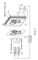
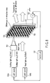
- the refractive index changing apparatus of the embodiment comprises light sources 101A and 101B, a control unit 102, an energy level control unit 103 for an electron injection unit, and a refractive index changeable element structure 104.
- the refractive index changeable element structure 104 comprises, for example, indium-tin oxide (ITO) transparent electrodes 105 as the electron injection unit, and a quantum structure 106 including a plurality of quantum dots and a barrier structure.
- the transparent electrodes 105 may be formed of glass plates providing the opposite sides of the index changeable element structure 104 and holding the quantum structure 106 therebetween.
- Quantum dots mean a 0 th dimensional electron system in which state density energy is made discrete by blocking in electrons in dot regions having a size substantially equal to the de Broglie wavelength of an electron.
- Quantum dots have discrete energy levels, and are formed of at least one selected from the group containing of metal fine particles, semiconductor fine particles, fullerene molecules, carbon nanotube and organic molecules. Further, in the barrier structure, electron tunneling occurs when the electron energy is substantially equal to the energy level of the quantum dots.
- the light sources 101A and 101B generate a light beam having energy designated by the control unit 102.
- the light beam generated by them is applied to the refractive index changeable element structure 104.
- the light source 101A generates, for example, excitation light beam for exciting the electrons of quantum dots in the refractive index changeable element structure 104.
- the light source 101B generates, for example, a read light beam for changing the refractive index the refractive index changeable element structure 104 to reproduce recorded images.
- the energy of the read light beam is set to a value that prevents the light beam from being completely absorbed by the quantum dots and barrier material. For instance, it is preferable that the energy is adjusted so that the transmittance of the light beam through the refractive index changeable element structure 104 is 50% or more. The energy of the excitation light will be described later in more detail, referring to FIG. 3.
- the control unit 102 controls the refractive index changing apparatus. It determines, for example, the intensity of the light beams emitted from the light sources 101A and 101B. Further, under the control of the control unit 102, the energy level control unit 103 for the electron injection unit controls the energy level of the electron injection unit to enable it to inject electrons into the refractive index changeable element structure 104.
- Electrons having energy designated by the energy level control unit 103 are injected from the electron injection unit 105 to the quantum structure 106, utilizing a tunneling effect that is acquired by controlling the energy level of the electron injection unit 105.
- the electron injection unit 105 may be formed of a pair of electrodes with the refractive index changeable element structure 104 interposed therebetween, or may be formed of the combination of the probe of a near-field scanning optical microscope (NSOM) and one of the ITO transparent electrodes 105. Electrons are injected into the quantum structure 106 by these elements.
- NOM near-field scanning optical microscope
- the refractive index changeable element structure 104 has a structure in which polystyrene films containing quantum dots are held between the ITO transparent electrodes 105.
- the quantum structure 106 includes quantum dots of, for example, C 60 and a barrier structure formed of the polystyrene films.
- the quantum dots are formed of at least one selected from the group consisting of metal fine particles, semiconductor fine particles, fullerene molecules, carbon nanotube and organic molecules.
- the barrier structure containing the quantum dots provides quantum dots having an energy level of a quantum-well type.
- the refractive index is related to the energy gap between the ground level (highest occupied molecular orbital (HOMO); single occupied molecular orbital (SOMO)) and the excited level (lowest unoccupied molecular orbital (LUMO)).
- a new outermost orbital i.e., a higher energy highest occupied molecular orbital
- the existing outermost orbital i.e., highest occupied molecular orbital
- the refractive index changing apparatus of the embodiment when electrons are injected from the electron injection unit 106 into the quantum structure 106, they are maintained on a new outermost orbital, which means that a change in the refractive index of the refractive index changeable element structure 104 is maintained. Accordingly, in the refractive index changing apparatus of the embodiment, once electrons are injected, it is not necessary to inject further energy from the electron injection unit 105. If the refractive index changing apparatus of the embodiment is regarded as a recording apparatus, the light source 101A, the energy level control unit 103 for the electron injection unit 105, and the electron injection unit 105 correspond to a write apparatus. Similarly, the quantum structure 106, into which electrons are injected, corresponds to a recording medium (refractive index changeable medium).
- the refractive index changing apparatus and method of the embodiment provide a new refractive-index-changing mechanism, and can realize a greater change in refractive index than the prior art.
- the structure of the refractive index changeable element structure 104 will be described.
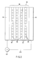
- the refractive index changeable element structure 104 comprises the ITO transparent electrodes 105 and quantum structure 106.
- the quantum structure 106 includes a barrier structure formed of a plurality of barrier layers 201, and a plurality of quantum dots 202.
- the quantum structure 106 is held between the two ITO transparent electrodes 105.
- the quantum structure 106 is formed by alternately stacking a barrier layer 201 containing quantum dots, and a barrier layer 201 containing no quantum dots.
- Each ITO transparent electrode (electron injection unit) 105 is connected to the energy level control unit 103 for the electron injection unit. Electrons are injected by a tunneling effect from one of the ITO transparent electrodes 105 to the quantum structure 106. It is preferable that each barrier layer 201 has a specific inductive capacity of 7 or more.
- the refractive index changeable element structure 104 is required to have an energy level of a quantum-well type, and includes the quantum dots 202 and barrier structure 201. Further, to enable electrons to be injected into the quantum dots 202 under the control of the control unit 102, the ITO transparent electrodes 105 and the energy level control unit 103 for them are provided. Furthermore, to keep the quantum dots 202 with electrons injected therein in a stable state, and to enable the relative relation between the Fermi level, which is energy level of the ITO transparent electrodes 105 into which electrons are injected, and the energy level of the quantum dots 202 to be changed, the energy level control unit 103 is connected to the ITO transparent electrodes 105. The injection of electrons will be described later with reference to FIG. 3.
- the refractive index changeable element structure 104 Since the refractive index changeable element structure 104 is an optical function element, it requires a light entrance unit and an emission unit.
- the ITO transparent electrodes 105 which are transparent, serve as the light entrance unit and the emission unit. In the case of FIG. 2, an exciting or read light beam enters one of the left and right ITO transparent electrodes 105, and a light beam having passed through the quantum structure 106 is emitted from the other of the left and right ITO transparent electrodes 105.
- the quantum dots may be formed of, for example, metal nano particles, semiconductor nano particles, organic molecules, etc.
- Typical nano particle materials of the quantum dots are metals, such as Cu, Au, Ag, Fe and Ni, III-V group semiconductors, such as Si, Ge, Sn, Pb, diamond, GaAs, AlAs, InAs, Gap and InSb, II-VI group semiconductors, such as ZnS, ZnSe, ZnTe, CdS, CdSe and CdTe, organic molecules, such as C 60 and carbon nanotube, and inorganic molecules.
- the barrier structure may preferably be formed of a material, such as glass and polymer, which has a large energy gap between the ground level (HOMO, SOMO) and the excited level (LUMO), and which does not absorb a light beam of a wavelength for exciting quantum dots.
- the material may preferably pass 50% or more a read light beam therethrough that has passed through the index changeable element structure 104.
- tertiary non-linear optical materials are not preferable because of the following reason. It is known that a tertiary non-linear optical material applies an electric field to quantum dots by a quantum effect to thereby modulate the wave function of an electron or exciter and increase the rage of change in refractive index. However, a change in refractive index due to a tertiary non-linear optical material is smaller by one, two or more digits than that in refractive index due to the refractive changing apparatus of the embodiment. In the tertiary non-linear optical effect, if the level of the electric field is increased, the change in refractive index is theoretically increased relatively.
- the material may well be broken by the strong electric field, and the rates of change reported so far fall within almost 1% or less.
- the barrier layer is made thick so that it can resist against a strong electric field.
- the light source 101A applies, to the index changeable element structure 104, a light beam having energy corresponding to the energy gap between the ground level G1 of each quantum dot and an excited level E1 just above the ground level.
- a light beam having energy corresponding to the energy gap between the ground level G1 of each quantum dot and an excited level E1 just above the ground level.
- one electron at the ground level G1 absorbs the energy of the exciting light beam and is excited to the excited level E1.
- the exciting light beam has energy resonant with the energy level of the quantum dots, and the energy of the exciting light beam is called resonant energy.
- the electron injection unit 105 injects an electron into a hole formed by the exciting light beam in a quantum dot at the ground level G1. Since one electron is injected into the hole at the ground level G1, no more electrons will drop from the excited level E1 to the ground level G1 while irradiating energy. Namely, when an electron is injected into a hole at the ground level G1, an electron at the excited level E1 can exist at this level in a stable manner.
- the energy level control unit 103 for the electron injection unit determines the energy level of an electron to be injected by the electron injection unit 105, in the following manner. Electrons existing at the ground level G1, excited level E1, etc., always acquire or emit energy depending upon temperature. Namely, the ground level G1, excited level E1, etc., widen their widths by the energy corresponding to temperature. If not influenced by temperature, it can be said that the energy level has no width like the delta function. Actually, however, assume that the energy level has a width corresponding to a state density distribution, and that the height or magnitude of the energy level includes all the width range.
- the width is determined in a narrow sense by the Fermi-Dirac distribution function, and is known to be substantially indicated by kT (k: Boltzmann constant [approximately 8.61 X 10 -5 (eV/K)]; T: Temperature (unit is K[kelvin]). Accordingly, it is sufficient if the energy level control unit 103 for the electron injection unit causes the electron injection unit 105 to inject, into the index changeable element structure 104, electrons having energy of the width kT around the ground level G1 (i.e., the energy between (G1 - kT) and (G1 + kT)).
- the energy level control unit 103 for the electron injection unit causes the electron injection unit 105 to inject, into the index changeable element structure 104, electrons having energy higher by kT than the ground level G1 (i.e., higher than G1 and lower than (G1 + kT)).
- the energy level control unit 103 for the electron injection unit causes the electric potential of the portion of the electron injection unit 105 connected to the index changeable element structure 104 to be increased to a value higher by kT (eV) or more than the ground level G1, the electrons at the ground level G1 cannot return to the electron injection unit 105. This prevents the electrons at the excited level from dropping to the ground level G1, and maintains them in a stable state.
- the energy level of the electron injection unit 105 is set higher by kT (eV) or more higher than the ground level of the quantum dots.
- kT eV
- the energy level control unit 103 has controlled the electron injection unit 105 to inject electrons into the quantum structure 106 by tunneling injection, and has stopped control after electron injection, the interaction between the electron injection unit and the ground level of the quantum dots will be none in practice.
- the electrons at the ground level G1 do not return to the electron injection unit 105, and the electrons at the excited level do not drop to the ground level G1 and keep in a stable state.
- the refractive index changing apparatus of the embodiment can prevent, from dropping to the ground level G1, electrons that are at the excited level when no power is consumed, i.e., can keep them in a stable state.
- the energy gap between the ground level G1 and the excited level E1 is greater than 2 kT.
- the difference between the ground level G1 and the energy level of the electron injection unit, and the difference between the excited level E1 and the energy level of the electron injection unit are each kT or more, a change in refractive index can be maintained with little power consumption.
- the energy higher by kT than the ground level G1 is set lower than the energy lower by kT than the excited level E1, in order to prevent the electron injection unit 105 from injecting electrons into quantum dots kept at the excited level E1.
- the energy lower by kT than the excited level E1 is set in light of the case where the excited level E1 is varied because of temperature. In other words, the condition that the excited level E1 is higher by 2 kT or more than the ground level G1 is also satisfied.
- the energy gap between the excited levels E1 and E2 of the quantum dots is greater than 2 kT.
- a tunneling barrier must be provided at a certain position between the electron injection unit 105 and the quantum dots that cause a change in refractive index. If a tunneling barrier is provided between the electron injection unit 105 and the quantum dots, no tunneling barrier may be provided between the quantum dots. However, in the quantum dots, discrete energy levels must be maintained.
- the real part of the complex refractive index is changed.
- the rate of change in refractive index when the electrons are kept excited is as high as 10% or more, which is higher by two digits or more than in the conventional non-linear optical materials.
- the change in the real part of the refractive index of the refractive index changeable element structure 104 caused by an exciting light beam ⁇ 1 emitted from the light source 101A enables a read light beam ⁇ 2, emitted from the light source 101B to the unit 104, to read therefrom a refractive-index-changed pattern written by the an exciting light beam, even though the unit 104 is transparent.
- the energy level of the electron injection unit is set to a value corresponding to energy slightly lower than the ground level G1 or excited level E1.
- the original state is recovered by generating a hole and emitting a light beam or by directly moving electrons from the quantum dots at the excited level E1 to the electron injection unit.
- the refractive index changing apparatus of the embodiment can be used as a recording apparatus for recording moving pictures, analog data, digital data, etc.
- electrons can be kept in an excited state, whereby the refractive index of the refractive index changeable element structure 104 can be kept stabilized, and the refractive index of part of the structure 104 can be changed.
- the tunneling effect of the electrons is utilized.
- the barrier structure 201 is thin, tunneling of electrons will easily occur.
- the tunneling effect depends upon the thickness of the barrier structure 201 that provides a tunneling barrier.
- the probability of occurrence of the tunneling effect can be computed based on the Schrödinger equation. The thinner the barrier structure 201, the more easily the tunneling effect occurs.
- the tunneling effect is a phenomenon occurring in a quantum mechanical system, in which when an electron of energy E lower than potential V 0 collides with a barrier of potential V 0 , it passes through the barrier. This occurs when the probability t is not zero both inside and outside the barrier.
- the rate of transmission of electrons through the barrier i.e., the probability t of the tunneling effect is given by the following equations (see, for example, Junji Haruyama, "Single Electron Tunneling-Quantum Mechanics and Nanotechnologies-", Corona Publishing co., ltd, Tokyo JAPAN, 2002, First Edition).
- the barrier structure 201 It is necessary to form the barrier structure 201 as thin as enables electrons to tunnel their ways through it. It is also necessary to set the charge energy (equal to an increase in the energy level of the quantum dots) of the barrier structure 201 higher than the ambient temperature energy kT (k: Boltzmann constant; T: absolute temperature). This means that it is necessary to make the electrostatic capacitance of the barrier structure 201 small, whereas the film thickness of the barrier structure 201, which is one of the factors for determining the electrostatic capacitance, must be set to such a low value as enables electrons to tunnel their ways through the barrier structure. In addition, the junction area, i.e., the surface area of the quantum dots, is very important, and it is necessary to form each quantum dot to a small size.
- the advantage of the refractive index changeable element of the embodiment remarkably differs from that acquired by the prior art in which the refractive index of a structure is changed using a secondary or tertiary non-linear optical effect represented by the Pockels effect. The differences therebetween will now be described.
- the light beam entering a quantum dot excites the electron shell by its electric field (excitation).
- the excited electron shell emits a light beam.
- the process of emission at this time relates to the Einstein B coefficient, and a certain time is required from excitation to emission even in a non-resonance region.
- a light beam propagates while repeating excitation and emission.
- the time required for excitation/emission determines the phase velocity Vp of light propagation. Assuming that the velocity of a light beam in vacuum is C, V p /C represents the real part of the refractive index changed by the refractive index changing apparatus of the embodiment.
- N A is the Avogadro number
- V mol is the volume of 1 mol (N A : 6.02 X 10 23 ).
- ⁇ M V mol
- the quantum dots are liable to be hard to stabilize.
- a dielectric is provided around the quantum dots as in the embodiment of the invention, the entire energy is stabilized because of dielectric relaxation, and the rate of change in polarizability is increased.
- electrons are injected, if the energy level of the LUMO of the barrier structure is set higher than that of each quantum dot, electrons are captured by the quantum dots.
- the voltage applied during injection of electrons can be roughly determined, regarding, as capacitors, dielectric members isolating the quantum dots from each other, and regarding the electrodes and capacitors as a series circuit.
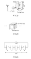
- a barrier structure with a thickness of 0.5 nm surrounds a cubic quantum dot having sides of 1 nm as shown in FIG. 4, and that five such cubic quantum dots arranged in series form capacitors as shown in FIG. 5.
- a voltage V is computed assuming that electrons are accumulated in the respective capacitors.
- the refractive index changing apparatus of the embodiment will be described using specific experimental examples.
- the barrier structure 201 is formed of polystyrene films, and the quantum dots 202 are formed of C 60 and dispersed in the polystyrene films.
- the polystyrene films containing the quantum dots 202 are stacked and held between the ITO transparent electrodes 105.
- each electrode (electron injection unit) 105 is connected to the energy level control unit 103 for the electron injection unit.
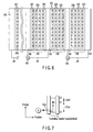
- the refractive index changeable element structure shown in FIG. 6 ten units, each of which is formed of the transparent electrodes 105 and the polystyrene films held therebetween, are attached together.
- control unit 102 instructed the electron injection unit 105 via the energy level control unit 103 to increase the energy level of the unit 105 to a value higher by 1.3 eV than the ground level G1 of the quantum dots, and instructed the light source 101A to stop the emission of a light beam.
- the pattern of the light beam was transferred to the polystyrene films containing C 60 in the form of a refractive index distribution figure.
- the rate of change in the refractive index of a portion to which a light beam of the highest intensity was emitted was about 10%. Since this change was the change in the real part of the complex refractive index, the pattern could be recognized also when a light beam other than an exciting light beam ⁇ 1, e.g., a read light beam of 0.95 eV, was emitted to the refractive index changeable element structure. Digital data, as well as the pattern, could be recorded at a time. In this example, since polystyrene films serve as tunneling barriers, it is not necessary to form no particular barrier film between each ITO transparent electrode 105 and each polystyrene film containing C 60 .
- the barrier structure 201 is formed of polystyrene, and the quantum dots 202 are formed of C 60 .
- Two exciting light beams ⁇ 3 and ⁇ 4 (each having an energy level of 2.7 eV and a wavelength of about 460 nm) were made to interfere with each other by an object lens 501.
- the resultant light beam was emitted to the refractive index changeable element structure of the experimental example 1, whereby a light spot of an interference pattern was recorded in the quantum structure 106.
- This recording corresponds to recording of digital data.
- the density of the interference pattern was about 9 patterns per 1 cm 2 .
- CdSe nano crystals with a diameter of about 1.2 nm were used as the quantum dots 202, instead of C 60 in the experimental example 1. Further, an exciting light beam of 3.0 eV (with a wavelength of 410 nm) and a read light beam of 0.8 eV (with a wavelength of 1.55 ⁇ m) were used. As a result, the same results as acquired in the experimental example 1 could be obtained.
- a light beam having energy capable of exciting, to an excited level, an electron of a ground level in a quantum dot that has discrete energy levels is emitted to the quantum dot. After that, an electron is injected into a position of the ground level in the quantum dot.
- a rate of change in refractive index that exceeds 1% can be acquired even in a transparent, and a change in refractive index can be recorded.
Landscapes
- Physics & Mathematics (AREA)
- Optics & Photonics (AREA)
- Chemical & Material Sciences (AREA)
- Engineering & Computer Science (AREA)
- Nanotechnology (AREA)
- Nonlinear Science (AREA)
- Life Sciences & Earth Sciences (AREA)
- Biophysics (AREA)
- Crystallography & Structural Chemistry (AREA)
- General Physics & Mathematics (AREA)
- Optical Modulation, Optical Deflection, Nonlinear Optics, Optical Demodulation, Optical Logic Elements (AREA)
- Semiconductor Lasers (AREA)
Abstract
Description
- The present invention relates to a refractive index changing apparatus and method.
- Many researchers have done so far research and development of refractive index changing materials (see, for example, Jpn. Pat. Appln. KOKAI Publication No. 2002-217488). This is because the refractive index determines the propagation characteristic of a light beam, therefore control of a light beam can be realized by controlling the refractive index and spatial distribution of refractive indices. Resulting from the success of the development of refractive index control techniques that utilize liquid crystal, liquid crystal displays have been produced. Moreover, since refractive index changing is regarded as a main technique for optical computers, many researches on secondary or tertiary non-linear optical materials that provide the Pockels effect or Kerr effect have been executed in the field of refractive index changing techniques.
- However, most changes in refractive index in a transparent region realized by the secondary or tertiary non-linear optical materials do not substantially exceed 1%. Although liquid crystal achieves a change of about 10% in refractive index, the use of liquid crystal is limited because it is a liquid. Further, when the supply of power to liquid crystal is stopped, records therein disappear.
- In accordance with an aspect of the invention, there is provided a refractive index changing apparatus comprising:
- a plurality of quantum dots each having discrete energy levels including an energy level of a ground state and an energy level of an excited state, the excited level being higher than the ground level even if energy due to an ambient temperature is provided on the quantum dots;
- a barrier structure unit formed of a dielectric which surrounds the quantum dots;
- an injection unit configured to inject an electron into a position of the ground level in each of the quantum dots via the barrier structure unit, utilizing a tunneling effect, or to prevent injection of an electron into the position, injecting the electron or preventing injection of the electron controlled by changing an energy level of the injection unit;
- a first light source which emits, to the quantum dots, a first light beam having first energy for exciting electrons from the ground level to the excited level; and
- a second light source which emits, to the quantum dots, a second light beam having second energy different from the first energy.
- In accordance with another aspect of the invention, there is provided a refractive index changing method comprising:
- emitting, to a plurality of quantum dots, a light beam for exciting an electron from a position of a ground level of each quantum dot to an excited level, the quantum dots each having discrete energy levels including the ground level and the excited level, the excited level being higher than the ground level even if energy due to an ambient temperature is provided on the quantum dots; and
- injecting the electrons into the ground level of each quantum dot utilizing a tunneling effect, or preventing the electrons from being injected into the ground level of each quantum dot by varying an energy level of an injection unit for injecting electrons into the quantum dots, via a barrier structure unit formed of a dielectric which surrounds the quantum dots.
- This summary of the invention does not necessarily describe all necessary features so that the invention may also be a sub-combination of these described features.
- The invention can be more fully understood from the following detailed description when taken in conjunction with the accompanying drawings, in which:
- FIG. 1 is a view illustrating a refractive index changing apparatus according to an embodiment of the invention;
- FIG. 2 is a view illustrating the refractive index changeable element structure;
- FIG. 3 is a view useful in explaining a phenomenon caused by an exciting light beam and electron injection utilizing an exciting light beam;
- FIG. 4 is a view illustrating quantum dots and a barrier structure model surrounding the dots;
- FIG. 5 is a view illustrating a circuit for generating a driving voltage used for electron injection;
- FIG. 6 is a schematic view illustrating connection example of the refractive index changeable element structure and energy
level control units 103 incorporated in an electron injection unit; - FIG. 7 is a view similar to FIG. 3, in which the quantum dot is C60; and
- FIG. 8 is a view illustrating a refractive index changing apparatus in which two exciting light beams are made to interfere each other by an object lens.
- A refractive index changing apparatus and method according to an embodiment of the invention will be described in detail with reference to the accompanying drawings.
- The embodiment has been developed in light of the above, and aims to provide a refractive index changing apparatus capable of achieving a rate of change in refractive index that exceeds 1% even in a transparent, and capable of recording a change in refractive index. The embodiment also aims to provide a refractive index changing method for use in the refractive index changing apparatus.
- The refractive index changing apparatus and method of the embodiment can exhibit a refractive index change of more than 1% in a transparent region, and can record the refractive index change.
- As shown in FIG. 1, the refractive index changing apparatus of the embodiment comprises
light sources control unit 102, an energylevel control unit 103 for an electron injection unit, and a refractive indexchangeable element structure 104. The refractive indexchangeable element structure 104 comprises, for example, indium-tin oxide (ITO)transparent electrodes 105 as the electron injection unit, and aquantum structure 106 including a plurality of quantum dots and a barrier structure. Thetransparent electrodes 105 may be formed of glass plates providing the opposite sides of the indexchangeable element structure 104 and holding thequantum structure 106 therebetween. - Quantum dots mean a 0th dimensional electron system in which state density energy is made discrete by blocking in electrons in dot regions having a size substantially equal to the de Broglie wavelength of an electron. Quantum dots have discrete energy levels, and are formed of at least one selected from the group containing of metal fine particles, semiconductor fine particles, fullerene molecules, carbon nanotube and organic molecules. Further, in the barrier structure, electron tunneling occurs when the electron energy is substantially equal to the energy level of the quantum dots.
- The
light sources control unit 102. The light beam generated by them is applied to the refractive indexchangeable element structure 104. Thelight source 101A generates, for example, excitation light beam for exciting the electrons of quantum dots in the refractive indexchangeable element structure 104. Thelight source 101B generates, for example, a read light beam for changing the refractive index the refractive indexchangeable element structure 104 to reproduce recorded images. Preferably, the energy of the read light beam is set to a value that prevents the light beam from being completely absorbed by the quantum dots and barrier material. For instance, it is preferable that the energy is adjusted so that the transmittance of the light beam through the refractive indexchangeable element structure 104 is 50% or more. The energy of the excitation light will be described later in more detail, referring to FIG. 3. - The
control unit 102 controls the refractive index changing apparatus. It determines, for example, the intensity of the light beams emitted from thelight sources control unit 102, the energylevel control unit 103 for the electron injection unit controls the energy level of the electron injection unit to enable it to inject electrons into the refractive indexchangeable element structure 104. - Electrons having energy designated by the energy
level control unit 103 are injected from theelectron injection unit 105 to thequantum structure 106, utilizing a tunneling effect that is acquired by controlling the energy level of theelectron injection unit 105. According to Schrödinger equation, unless the barrier layer is thin, the probability of occurrence of the tunneling effect is remarkably low, therefore the barrier layer must be formed relatively thin. Concerning the thickness of the barrier layer, a description will be given later with reference to FIG. 3. Theelectron injection unit 105 may be formed of a pair of electrodes with the refractive indexchangeable element structure 104 interposed therebetween, or may be formed of the combination of the probe of a near-field scanning optical microscope (NSOM) and one of the ITOtransparent electrodes 105. Electrons are injected into thequantum structure 106 by these elements. - The refractive index
changeable element structure 104 has a structure in which polystyrene films containing quantum dots are held between the ITOtransparent electrodes 105. Thequantum structure 106 includes quantum dots of, for example, C60 and a barrier structure formed of the polystyrene films. The quantum dots are formed of at least one selected from the group consisting of metal fine particles, semiconductor fine particles, fullerene molecules, carbon nanotube and organic molecules. In thequantum structure 106, the barrier structure containing the quantum dots provides quantum dots having an energy level of a quantum-well type. - The principle of the refractive index changing apparatus according to the embodiment will be described.
- The refractive index is related to the energy gap between the ground level (highest occupied molecular orbital (HOMO); single occupied molecular orbital (SOMO)) and the excited level (lowest unoccupied molecular orbital (LUMO)).
- When the
electron injection unit 105 has injected electrons into the quantum dots of thequantum structure 106, a new outermost orbital (i.e., a higher energy highest occupied molecular orbital) is formed outside the existing outermost orbital (i.e., highest occupied molecular orbital) that significantly contributes to the determination of the refractive index. If this new outermost orbital is maintained, a great refractive index change effect is maintained. - Thus, in the embodiment of the invention, when electrons are injected from the
electron injection unit 106 into thequantum structure 106, they are maintained on a new outermost orbital, which means that a change in the refractive index of the refractive indexchangeable element structure 104 is maintained. Accordingly, in the refractive index changing apparatus of the embodiment, once electrons are injected, it is not necessary to inject further energy from theelectron injection unit 105. If the refractive index changing apparatus of the embodiment is regarded as a recording apparatus, thelight source 101A, the energylevel control unit 103 for theelectron injection unit 105, and theelectron injection unit 105 correspond to a write apparatus. Similarly, thequantum structure 106, into which electrons are injected, corresponds to a recording medium (refractive index changeable medium). - The refractive index changing apparatus and method of the embodiment provide a new refractive-index-changing mechanism, and can realize a greater change in refractive index than the prior art.
- Referring now to FIG. 2, the structure of the refractive index
changeable element structure 104 will be described. - As shown in FIG. 2, the refractive index
changeable element structure 104 comprises the ITOtransparent electrodes 105 andquantum structure 106. Thequantum structure 106 includes a barrier structure formed of a plurality of barrier layers 201, and a plurality ofquantum dots 202. - As can be understood from FIG. 2, the
quantum structure 106 is held between the two ITOtransparent electrodes 105. Thequantum structure 106 is formed by alternately stacking abarrier layer 201 containing quantum dots, and abarrier layer 201 containing no quantum dots. Each ITO transparent electrode (electron injection unit) 105 is connected to the energylevel control unit 103 for the electron injection unit. Electrons are injected by a tunneling effect from one of the ITOtransparent electrodes 105 to thequantum structure 106. It is preferable that eachbarrier layer 201 has a specific inductive capacity of 7 or more. - The refractive index
changeable element structure 104 is required to have an energy level of a quantum-well type, and includes thequantum dots 202 andbarrier structure 201. Further, to enable electrons to be injected into thequantum dots 202 under the control of thecontrol unit 102, the ITOtransparent electrodes 105 and the energylevel control unit 103 for them are provided. Furthermore, to keep thequantum dots 202 with electrons injected therein in a stable state, and to enable the relative relation between the Fermi level, which is energy level of the ITOtransparent electrodes 105 into which electrons are injected, and the energy level of thequantum dots 202 to be changed, the energylevel control unit 103 is connected to the ITOtransparent electrodes 105. The injection of electrons will be described later with reference to FIG. 3. - Since the refractive index
changeable element structure 104 is an optical function element, it requires a light entrance unit and an emission unit. The ITOtransparent electrodes 105, which are transparent, serve as the light entrance unit and the emission unit. In the case of FIG. 2, an exciting or read light beam enters one of the left and right ITOtransparent electrodes 105, and a light beam having passed through thequantum structure 106 is emitted from the other of the left and right ITOtransparent electrodes 105. - The quantum dots may be formed of, for example, metal nano particles, semiconductor nano particles, organic molecules, etc. Typical nano particle materials of the quantum dots are metals, such as Cu, Au, Ag, Fe and Ni, III-V group semiconductors, such as Si, Ge, Sn, Pb, diamond, GaAs, AlAs, InAs, Gap and InSb, II-VI group semiconductors, such as ZnS, ZnSe, ZnTe, CdS, CdSe and CdTe, organic molecules, such as C60 and carbon nanotube, and inorganic molecules. Further, the barrier structure may preferably be formed of a material, such as glass and polymer, which has a large energy gap between the ground level (HOMO, SOMO) and the excited level (LUMO), and which does not absorb a light beam of a wavelength for exciting quantum dots. The material may preferably pass 50% or more a read light beam therethrough that has passed through the index
changeable element structure 104. - As the material of the barrier structure, tertiary non-linear optical materials are not preferable because of the following reason. It is known that a tertiary non-linear optical material applies an electric field to quantum dots by a quantum effect to thereby modulate the wave function of an electron or exciter and increase the rage of change in refractive index. However, a change in refractive index due to a tertiary non-linear optical material is smaller by one, two or more digits than that in refractive index due to the refractive changing apparatus of the embodiment. In the tertiary non-linear optical effect, if the level of the electric field is increased, the change in refractive index is theoretically increased relatively. Actually, however, the material may well be broken by the strong electric field, and the rates of change reported so far fall within almost 1% or less. Further, in the case of utilizing the tertiary non-linear optical effect, no electrons are injected unlike the refractive index changing apparatus of the embodiment, and in general, the barrier layer is made thick so that it can resist against a strong electric field.
- Referring to FIG. 3, a phenomenon concerning a exciting light beam generated by the
light source 101A will be described. - As shown in FIG. 3, the
light source 101A applies, to the indexchangeable element structure 104, a light beam having energy corresponding to the energy gap between the ground level G1 of each quantum dot and an excited level E1 just above the ground level. At this time, one electron at the ground level G1 absorbs the energy of the exciting light beam and is excited to the excited level E1. The exciting light beam has energy resonant with the energy level of the quantum dots, and the energy of the exciting light beam is called resonant energy. - Further, at this time, the
electron injection unit 105 injects an electron into a hole formed by the exciting light beam in a quantum dot at the ground level G1. Since one electron is injected into the hole at the ground level G1, no more electrons will drop from the excited level E1 to the ground level G1 while irradiating energy. Namely, when an electron is injected into a hole at the ground level G1, an electron at the excited level E1 can exist at this level in a stable manner. - More specifically, the energy
level control unit 103 for the electron injection unit determines the energy level of an electron to be injected by theelectron injection unit 105, in the following manner. Electrons existing at the ground level G1, excited level E1, etc., always acquire or emit energy depending upon temperature. Namely, the ground level G1, excited level E1, etc., widen their widths by the energy corresponding to temperature. If not influenced by temperature, it can be said that the energy level has no width like the delta function. Actually, however, assume that the energy level has a width corresponding to a state density distribution, and that the height or magnitude of the energy level includes all the width range. The width is determined in a narrow sense by the Fermi-Dirac distribution function, and is known to be substantially indicated by kT (k: Boltzmann constant [approximately 8.61 X 10⁻⁵ (eV/K)]; T: Temperature (unit is K[kelvin]). Accordingly, it is sufficient if the energylevel control unit 103 for the electron injection unit causes theelectron injection unit 105 to inject, into the indexchangeable element structure 104, electrons having energy of the width kT around the ground level G1 (i.e., the energy between (G1 - kT) and (G1 + kT)). More preferably, the energylevel control unit 103 for the electron injection unit causes theelectron injection unit 105 to inject, into the indexchangeable element structure 104, electrons having energy higher by kT than the ground level G1 (i.e., higher than G1 and lower than (G1 + kT)). When the energylevel control unit 103 for the electron injection unit causes the electric potential of the portion of theelectron injection unit 105 connected to the indexchangeable element structure 104 to be increased to a value higher by kT (eV) or more than the ground level G1, the electrons at the ground level G1 cannot return to theelectron injection unit 105. This prevents the electrons at the excited level from dropping to the ground level G1, and maintains them in a stable state. - Further, in the embodiment, where the energy
level control unit 103 does not control theelectron injection unit 105, the energy level of theelectron injection unit 105 is set higher by kT (eV) or more higher than the ground level of the quantum dots. When the energylevel control unit 103 has controlled theelectron injection unit 105 to inject electrons into thequantum structure 106 by tunneling injection, and has stopped control after electron injection, the interaction between the electron injection unit and the ground level of the quantum dots will be none in practice. As a result, the electrons at the ground level G1 do not return to theelectron injection unit 105, and the electrons at the excited level do not drop to the ground level G1 and keep in a stable state. - Thus, the refractive index changing apparatus of the embodiment can prevent, from dropping to the ground level G1, electrons that are at the excited level when no power is consumed, i.e., can keep them in a stable state. In this case, it is necessary to prepare materials for the quantum dots and the electron injection unit, which enable each of the ground level G1 and the excited level E1 to be kept different from the energy level of the electron injection unit, regardless of variations in the energy level of electrons due to temperature. Namely, in the quantum dots, the energy gap between the ground level G1 and the excited level E1 is greater than 2 kT. If the difference between the ground level G1 and the energy level of the electron injection unit, and the difference between the excited level E1 and the energy level of the electron injection unit are each kT or more, a change in refractive index can be maintained with little power consumption. Further, when this condition is satisfied, the energy higher by kT than the ground level G1 is set lower than the energy lower by kT than the excited level E1, in order to prevent the
electron injection unit 105 from injecting electrons into quantum dots kept at the excited level E1. The energy lower by kT than the excited level E1 is set in light of the case where the excited level E1 is varied because of temperature. In other words, the condition that the excited level E1 is higher by 2 kT or more than the ground level G1 is also satisfied. - It is also preferable to prepare a material for the quantum dots that prevents the excited level E1 from becoming equal to or more than an excited level E2 set higher than the level E1, even if the energy level is destabilized because of the disturbance of electrons by temperature. Namely, it is preferable that the energy gap between the excited levels E1 and E2 of the quantum dots is greater than 2 kT.
- A tunneling barrier must be provided at a certain position between the
electron injection unit 105 and the quantum dots that cause a change in refractive index. If a tunneling barrier is provided between theelectron injection unit 105 and the quantum dots, no tunneling barrier may be provided between the quantum dots. However, in the quantum dots, discrete energy levels must be maintained. - In contrast, if a tunneling barrier is provided between the quantum dots, it is not necessary to provide a tunneling barrier between the surface of the group of the quantum dots and the
electron injection unit 105. In this case, the quantum dots located at the surface of the group function as part of theelectron injection unit 105. If the difference between the Fermi level (= electron energy level of the electron injection unit 105) and the ground level or excited level of the quantum dots is small, electrons excited to the excited level by an exciting light beam will soon drop to the ground level. In other words, the electrons at the excited level are varied in level by the energy of temperature, whereby the electrons and holes will be recombined soon. Unless no electron exists at the excited level, no change in refractive index occurs. Therefore, the energylevel control unit 103 for the electron injection unit determines from the energy level of the electrode whether the refractive index should be varied. - Where the electron-excited state is kept as described above, the real part of the complex refractive index is changed. The greater the difference between the energy gap of the excited levels E1 and E2 and that of the ground level G1 and the excited level E1, the greater the rate of change of the real part. Further, the smaller the dot size, the lower the electron density at the excited level E1, and the more easily saturation occurs, the greater the change in refractive index. The rate of change in refractive index when the electrons are kept excited is as high as 10% or more, which is higher by two digits or more than in the conventional non-linear optical materials.
- The change in the real part of the refractive index of the refractive index
changeable element structure 104 caused by an exciting light beam ω1 emitted from thelight source 101A enables a read light beam ω2, emitted from thelight source 101B to theunit 104, to read therefrom a refractive-index-changed pattern written by the an exciting light beam, even though theunit 104 is transparent. On the other hand, to release the excited state of electrons, the energy level of the electron injection unit is set to a value corresponding to energy slightly lower than the ground level G1 or excited level E1. As a result, the original state is recovered by generating a hole and emitting a light beam or by directly moving electrons from the quantum dots at the excited level E1 to the electron injection unit. Thus, a refractive-index-changed pattern recorded in the refractive indexchangeable element structure 104 is deleted. As described above, the refractive index changing apparatus of the embodiment can be used as a recording apparatus for recording moving pictures, analog data, digital data, etc. - As described above, in the refractive index changing apparatus of the embodiment, electrons can be kept in an excited state, whereby the refractive index of the refractive index
changeable element structure 104 can be kept stabilized, and the refractive index of part of thestructure 104 can be changed. - To inject electrons into the
quantum structure 106, the tunneling effect of the electrons is utilized. When thebarrier structure 201 is thin, tunneling of electrons will easily occur. The tunneling effect depends upon the thickness of thebarrier structure 201 that provides a tunneling barrier. The probability of occurrence of the tunneling effect can be computed based on the Schrödinger equation. The thinner thebarrier structure 201, the more easily the tunneling effect occurs. - More specifically, the tunneling effect is a phenomenon occurring in a quantum mechanical system, in which when an electron of energy E lower than potential V0 collides with a barrier of potential V0, it passes through the barrier. This occurs when the probability t is not zero both inside and outside the barrier. According to the Schrodinger equation, the rate of transmission of electrons through the barrier, i.e., the probability t of the tunneling effect is given by the following equations (see, for example, Junji Haruyama, "Single Electron Tunneling-Quantum Mechanics and Nanotechnologies-", Corona Publishing co., ltd, Tokyo JAPAN, 2002, First Edition).


where m0 represents the mass of an electron, h a Dirac constant (= h / 2π ), and a the thickness of a tunneling barrier. - From these equations, it can be understood that the thinner the thickness a of the barrier, the more easily tunneling occurs.
- Further, when electrons are injected into the
quantum dots 202 accumulated in thequantum structure 106 and having discrete energy levels, coulomb blockade may occur. When coulomb blockade occurs, electrons are trapped by thequantum dots 202 and stabilized. To cause coulomb blockade to occur, the following three conditions must be satisfied:


where k is the Boltzmann constant, T is the temperature, RT is the junction tunneling resistance, RQ is the resistance quantum (25.8 kΩ), and Re(Zt(ω)) is the real part of an environmental impedance in electromagnetic field. Further, EC represents charge energy given by the following equation:
where Cj is the junction capacitance given by the following equation:
where ε is the dielectric constant, and S is the junction area. - It is necessary to form the
barrier structure 201 as thin as enables electrons to tunnel their ways through it. It is also necessary to set the charge energy (equal to an increase in the energy level of the quantum dots) of thebarrier structure 201 higher than the ambient temperature energy kT (k: Boltzmann constant; T: absolute temperature). This means that it is necessary to make the electrostatic capacitance of thebarrier structure 201 small, whereas the film thickness of thebarrier structure 201, which is one of the factors for determining the electrostatic capacitance, must be set to such a low value as enables electrons to tunnel their ways through the barrier structure. In addition, the junction area, i.e., the surface area of the quantum dots, is very important, and it is necessary to form each quantum dot to a small size. - In light of the energy level, coulomb blockade is determined based on the relationship between the Fermi level (= energy level of the electrode)and the energy level (EC) of the quantum dots into which an electron is injected by tunneling. It is sufficient if EC is varied by kT or more when one electron is injected.
- The advantage of the refractive index changeable element of the embodiment remarkably differs from that acquired by the prior art in which the refractive index of a structure is changed using a secondary or tertiary non-linear optical effect represented by the Pockels effect. The differences therebetween will now be described.
- (1) In the prior art, electrons are kept in the electrodes for applying an electric field to a structure. In contrast, in the embodiment of the invention, electrons are moved from the electron injection unit (electrode) to quantum dots contained in the structure.
- (2) In the prior art, when the application of a voltage to the structure is stopped, the non-linear optical effect and hence the refractive index changed state disappear. In contrast, in the embodiment of the invention, as long as electrons stay in the quantum dots, the refractive index changed state is kept.
- (3) In the Pockels effect of the prior art, the rate of change in refractive index is as low as about 10-3. In contrast, in the embodiment of the invention, the rage of change is 10-1 or more.
- (4) In general, there are some methods, such as photochromism, for changing absorption spectra. Further, as can be understood from Kramers-Krönig relation, a relatively great change in refractive index near the light-absorbing end of the
quantum structure 106 can be realized. Accordingly, a method for changing the absorption spectrum or absorption coefficient to change the real part of the refractive index is often utilized. However, it is difficult to significantly change the refractive index in a transparent region. On the other hand, in the embodiment of the invention, a great change in refractive index can be realized even in a transparent region. - (5) In the case of a general three-dimensional bulk semiconductor, a large number of charges exist in a single excited band branch, therefore when a single electron is injected, little change occurs in the distribution of electrons that occupy the band (energy level) branch. In contrast, in the embodiment of the invention, since the quantum dots have discrete energy levels, only a small number of electrons exist at each energy level. Therefore, if a new single electron is injected into a quantum dot, it occupies an energy level that has not been occupied so far. Further, since the quantum dots have discrete energy levels, the width of each absorption spectrum is narrow and hence a large transparent region is left.
- (6) The refractive index changing element according to the embodiment of the invention aims to control the transmission/reflection of a light beam and to optically record information, which differs from a laser or amplifier that utilizes absorption or resonance of a light beam. Therefore, the wider the wavelength region that can transmit a light beam therethrough, the wider the application range of the refractive index changing element as an optical device. Moreover, the embodiment of the invention differs in both principle and advantage from the quantum-dot exciter for amplifying the tertiary non-linear optical effect utilizing an absorption/resonance effect. Namely, the embodiment provides the advantage that the refractive index can be changed even in a transparent region.
- (7) In the embodiment of the invention, the portion of the refractive index
changeable element structure 104 other than the quantum dots does not change in refractive index. Therefore, the higher the density of the quantum dots, the greater the rate of change in the refractive index of theentire unit 104. When the refractive index changing element of the embodiment is used as a waveguide, it is advantageous to set the density of the quantum dots so that the rate of change in refractive index at least exceeds 1.5%. 1.5% is a general value to which the rate of change in the refractive index of a currently used waveguide is set. - In relation to the above-described differences, a further description will be given of the principle of the refractive index changing element. The light beam entering a quantum dot excites the electron shell by its electric field (excitation). The excited electron shell emits a light beam. The process of emission at this time relates to the Einstein B coefficient, and a certain time is required from excitation to emission even in a non-resonance region. A light beam propagates while repeating excitation and emission. The time required for excitation/emission determines the phase velocity Vp of light propagation. Assuming that the velocity of a light beam in vacuum is C, Vp/C represents the real part of the refractive index changed by the refractive index changing apparatus of the embodiment. The refractive index is related to the molecular polarizability by the following Lorentz-Lorenz equation:


where NA is the Avogadro number, and Vmol is the volume of 1 mol (NA: 6.02 X 10²³). Further, the following equation is established:
- Therefore, the following equation (Lorentz-Lorenz equation) can be derived:

where n is the refractive index, M is the mass of 1 mol, p is the density, and α is the polarizability. - In general, to change the molecular polarizability, an electric field is applied to distort the orbital of an electron, utilizing the secondary or tertiary non-linear optical effect. However, the rate of change in polarizability realized by this method is low. In contrast, when an electron is injected into a quantum dot of a nano scale, a new orbital is formed and coulomb repulsion occurs, whereby the chemical potentials of HOMO or LUMO and the energy gap between HOMO and LUMO are significantly changed. As the effect of this, the polarizability is also significantly changed. On the other hand, when an electron is emitted from a quantum dot, no new orbital is formed, with the result that the rate of change in polarizability is lower than in the case of injecting an electron into a quantum dot. However, even when an electron is emitted from a quantum dot, a greater polarizability change can be expected than in the prior art where polarizability change is achieved by a non-linear optical effect.
- Further, in general, when an excessive number of electrons are injected into quantum dots, the quantum dots are liable to be hard to stabilize. On the other hand, if a dielectric is provided around the quantum dots as in the embodiment of the invention, the entire energy is stabilized because of dielectric relaxation, and the rate of change in polarizability is increased. When electrons are injected, if the energy level of the LUMO of the barrier structure is set higher than that of each quantum dot, electrons are captured by the quantum dots.
- The voltage applied during injection of electrons can be roughly determined, regarding, as capacitors, dielectric members isolating the quantum dots from each other, and regarding the electrodes and capacitors as a series circuit. As a model, it is assumed that a barrier structure with a thickness of 0.5 nm surrounds a cubic quantum dot having sides of 1 nm as shown in FIG. 4, and that five such cubic quantum dots arranged in series form capacitors as shown in FIG. 5. A voltage V is computed assuming that electrons are accumulated in the respective capacitors. The relationship V = Q/C is established between the voltage V, the capacitance C of each capacitor and the charge Q. Further, C is given by the following equation:

- In the above model, S = 1 X 10-18m2, and d = 1 X 1-10-9 X 5 [m]. The total thickness including the quantum dots is 10 nm. Further, since the charge Q corresponds to the five electrons injected into the quantum dots, Q = e X 5 = 1.6 X 10⁻¹⁹[C] X 5 = 8 X 10-19[C]
- If εr = 10, C = 1.8 X 10⁻²⁰, therefore V is approximately 44V. Assuming that the total thickness is 100 nm, if εr = 10, V is about 440 volts, while if εr = 100, V is approximately 44 volts. Further, if εr = 1000, V is about 4.4 volts. Thus, electrons can be easily injected. In the above model, εr is approximately 880 and the driving voltage is about 5 volts. In light of the driving voltage, this relative dielectric constant is preferable. To increase the thickness, the electrodes may be each formed of a plurality of layers. Further, no problem will occur even if the quantum dots are arranged in parallel with the electrodes.
- The refractive index changing apparatus of the embodiment will be described using specific experimental examples.
- Referring to FIG. 6, a description will be given of a specific experimental example in which the refractive index
changeable element structure 104 is modified. - In this example, the
barrier structure 201 is formed of polystyrene films, and thequantum dots 202 are formed of C60 and dispersed in the polystyrene films. The polystyrene films containing thequantum dots 202 are stacked and held between the ITOtransparent electrodes 105. To permit the potential difference of the ITOtransparent electrodes 105 to be changed, each electrode (electron injection unit) 105 is connected to the energylevel control unit 103 for the electron injection unit. In the refractive index changeable element structure shown in FIG. 6, ten units, each of which is formed of thetransparent electrodes 105 and the polystyrene films held therebetween, are attached together. - As shown in FIG. 6, voltages were applied to the respective pairs of ITO
transparent electrodes 105 so that the electrodes are alternately set to 0 volt (ground voltage), a predetermined Voltage V, 0 volt, the voltage V, ..., from one outermost electrode to the other outermost electrode. In this state, firstly, thecontrol unit 102 controlled the power voltage V to make it correspond to the ground level G1 shown in FIG. 3. Subsequently, thecontrol unit 102 caused thelight source 101A to emit an exciting light beam of 2.7 eV having a pattern to be recorded in the refractive indexchangeable element structure 104. After that, thecontrol unit 102 instructed theelectron injection unit 105 via the energylevel control unit 103 to increase the energy level of theunit 105 to a value higher by 1.3 eV than the ground level G1 of the quantum dots, and instructed thelight source 101A to stop the emission of a light beam. As a result, it was found that the pattern of the light beam was transferred to the polystyrene films containing C60 in the form of a refractive index distribution figure. - In this example, the rate of change in the refractive index of a portion to which a light beam of the highest intensity was emitted was about 10%. Since this change was the change in the real part of the complex refractive index, the pattern could be recognized also when a light beam other than an exciting light beam ω1, e.g., a read light beam of 0.95 eV, was emitted to the refractive index changeable element structure. Digital data, as well as the pattern, could be recorded at a time. In this example, since polystyrene films serve as tunneling barriers, it is not necessary to form no particular barrier film between each ITO
transparent electrode 105 and each polystyrene film containing C60. - Furthermore, the same results as the above could be acquired even when a disk-shaped refractive index changeable element structure was formed, a light beam is emitted to this unit while rotating it, thereby recording data, and then reproducing the data by applying a read light beam to the data-recorded unit.
- Referring to FIG. 7, another description will be given of the case where the
barrier structure 201 is formed of polystyrene, and thequantum dots 202 are formed of C60. - In the case of C60 shown in FIG. 7, if, for example, the temperature of the quantum dots in the
quantum structure 106 included in the refractive indexchangeable element structure 104 is 300K, kT indicating the degree of destabilization of energy due to temperature is about 0.026 eV. Further, in the case of C60 shown in FIG. 7, since the energy gap between the ground level G1 and the excited level E1 is 2.7 eV, which is higher than 2 kT (= about 0.052 eV). In addition, in the case of C60 shown in FIG. 7, since the energy gap between the excited levels E1 and E2 is 1.4 eV, which is also higher than 2 kT (= about 0.052 eV). - In the experimental example 1, if the ITO transparent electrodes as the electron injection unit were formed of gold, when the application of the voltage was stopped, the refractive index pattern disappeared. However, when the ITO transparent electrodes were formed of cesium, the pattern was left even after the application of the voltage was stopped.
- In a third experimental example, two exciting light beams are made to interfere with each other by an object lens, and the resultant interference pattern is recorded in the
quantum structure 106. This example will be described with reference to FIG. 8. - Two exciting light beams ω3 and ω4 (each having an energy level of 2.7 eV and a wavelength of about 460 nm) were made to interfere with each other by an
object lens 501. The resultant light beam was emitted to the refractive index changeable element structure of the experimental example 1, whereby a light spot of an interference pattern was recorded in thequantum structure 106. This recording corresponds to recording of digital data. The density of the interference pattern was about 9 patterns per 1 cm2. After that, when a light beam (read light beam) of 0.95 eV (with a wavelength of 1.3 µm) was emitted with a beam area of 1 cm2 from thelight source 101B, the light beam was diffracted at 9 points, thereby simultaneously reading data included in a beam spot. - In this example, CdSe nano crystals with a diameter of about 1.2 nm were used as the
quantum dots 202, instead of C60 in the experimental example 1. Further, an exciting light beam of 3.0 eV (with a wavelength of 410 nm) and a read light beam of 0.8 eV (with a wavelength of 1.55 µm) were used. As a result, the same results as acquired in the experimental example 1 could be obtained. - As described above, in the refractive index changing apparatus and method according to the embodiment of the invention, a light beam having energy capable of exciting, to an excited level, an electron of a ground level in a quantum dot that has discrete energy levels is emitted to the quantum dot. After that, an electron is injected into a position of the ground level in the quantum dot. As a result, a rate of change in refractive index that exceeds 1% can be acquired even in a transparent, and a change in refractive index can be recorded.
Claims (10)
- A refractive index changing apparatus characterized by comprising:a plurality of quantum dots (106) each having discrete energy levels including an energy level of a ground state and an energy level of an excited state, the excited level being higher than the ground level even if energy due to an ambient temperature is provided on the quantum dots;a barrier structure (106) formed of a dielectric which surrounds the quantum dots;means (105) for injecting an electron into a position of the ground level in each of the quantum dots via the barrier structure, utilizing a tunneling effect, or to prevent injection of an electron into the position, injecting the electron or preventing injection of the electron controlled by changing an energy level of the injection unit;means (101A) for emitting, to the quantum dots, a first light beam having first energy for exciting electrons from the ground level to the excited level; andmeans (101B) for emitting, to the quantum dots, a second light beam having second energy different from the first energy.
- The apparatus according to claim 1, characterized in that when no voltage is applied to the injecting means, a first difference between the energy level of the injecting means and the ground level of each quantum dot is not less than the energy due to the ambient temperature, and a second difference between the energy level of the injecting means and the excited level of each quantum dot is not less than the energy due to the ambient temperature.
- The apparatus according to claim 1 or 2, characterized in that the energy level of the injecting means falls within a width, the ground level of each quantum dot being varied within the width by the energy due to the ambient temperature.
- The apparatus according to claim 1 or 2, characterized in that the energy level of the injecting means is higher than the ground level of each quantum dot by the energy due to the ambient temperature.
- The apparatus according to claim 1, 2, 3 or 4, characterized in that the injecting means includes two transparent electrodes (105) between which the barrier structure is interposed, and a voltage applying unit which applies a voltage to each of the transparent electrodes.
- The apparatus according to claim 1, 2, 3, 4 or 5, characterized in that an energy gap between the ground level and the excited level of each of the quantum dots is higher than 2 kT, k representing a Boltzmann constant, T representing an ambient temperature.
- The apparatus according to claim 1, 2, 3, 4 or 5, characterized in that an energy gap between the ground level and the excited level of each quantum dot is higher than energy defined by a Fermi-Dirac distribution function.
- The apparatus according to claim 1, 2, 3, 4, 5, 6 or 7, characterized in that each of the quantum dots is formed of at least one selected from a group containing a metal fine particle, a semiconductor fine particle, a fullerene molecule, a carbon nanotube and an organic molecule.
- A refractive index changing method characterized by comprising:emitting, to a plurality of quantum dots (106), a light beam for exciting an electron from a position of a ground level of each quantum dot to an excited level, the quantum dots each having discrete energy levels including the ground level and the excited level, the excited level being higher than the ground level even if energy due to an ambient temperature is provided on the quantum dots; andinjecting the electrons into the ground level of each quantum dot utilizing a tunneling effect, or preventing the electrons from being injected into the ground level of each quantum dot by varying an energy level of an injecting means for injecting electrons into the quantum dots, via a barrier structure unit formed of a dielectric which surrounds the quantum dots.
- The method according to claim 9, characterized in that the energy level of the injecting means falls within a width, the ground level of each quantum dot being varied within the width by the energy due to the ambient temperature.
Applications Claiming Priority (1)
| Application Number | Priority Date | Filing Date | Title |
|---|---|---|---|
| JP2004287960A JP3987519B2 (en) | 2004-09-30 | 2004-09-30 | Refractive index changing device and refractive index changing method |
Publications (2)
| Publication Number | Publication Date |
|---|---|
| EP1643294A2 true EP1643294A2 (en) | 2006-04-05 |
| EP1643294A3 EP1643294A3 (en) | 2007-05-23 |
Family
ID=35510942
Family Applications (1)
| Application Number | Title | Priority Date | Filing Date |
|---|---|---|---|
| EP05256064A Withdrawn EP1643294A3 (en) | 2004-09-30 | 2005-09-29 | Refractive index changing apparatus and method |
Country Status (3)
| Country | Link |
|---|---|
| US (1) | US7372067B2 (en) |
| EP (1) | EP1643294A3 (en) |
| JP (1) | JP3987519B2 (en) |
Families Citing this family (25)
| Publication number | Priority date | Publication date | Assignee | Title |
|---|---|---|---|---|
| JP3987519B2 (en) | 2004-09-30 | 2007-10-10 | 株式会社東芝 | Refractive index changing device and refractive index changing method |
| JP4372048B2 (en) * | 2005-05-30 | 2009-11-25 | 株式会社東芝 | Refractive index change element |
| US9951438B2 (en) | 2006-03-07 | 2018-04-24 | Samsung Electronics Co., Ltd. | Compositions, optical component, system including an optical component, devices, and other products |
| JP2007328188A (en) * | 2006-06-08 | 2007-12-20 | Toshiba Corp | Near-field interaction control element |
| JP4469871B2 (en) * | 2007-03-28 | 2010-06-02 | 株式会社東芝 | Optical waveguide |
| US20080292979A1 (en) * | 2007-05-22 | 2008-11-27 | Zhe Ding | Transparent conductive materials and coatings, methods of production and uses thereof |
| JP5773646B2 (en) | 2007-06-25 | 2015-09-02 | キユーデイー・ビジヨン・インコーポレーテツド | Compositions and methods comprising depositing nanomaterials |
| US9136498B2 (en) * | 2007-06-27 | 2015-09-15 | Qd Vision, Inc. | Apparatus and method for modulating photon output of a quantum dot light emitting device |
| WO2009014707A2 (en) | 2007-07-23 | 2009-01-29 | Qd Vision, Inc. | Quantum dot light enhancement substrate and lighting device including same |
| US20090056589A1 (en) * | 2007-08-29 | 2009-03-05 | Honeywell International, Inc. | Transparent conductors having stretched transparent conductive coatings and methods for fabricating the same |
| JP4477052B2 (en) | 2007-10-03 | 2010-06-09 | 株式会社東芝 | Method for producing metal nanoparticle inorganic composite and metal nanoparticle inorganic composite |
| US7727578B2 (en) * | 2007-12-27 | 2010-06-01 | Honeywell International Inc. | Transparent conductors and methods for fabricating transparent conductors |
| US7642463B2 (en) * | 2008-01-28 | 2010-01-05 | Honeywell International Inc. | Transparent conductors and methods for fabricating transparent conductors |
| ATE530342T1 (en) * | 2008-01-28 | 2011-11-15 | Hitachi Ind Equipment Sys | INKJET RECORDING APPARATUS |
| US7960027B2 (en) * | 2008-01-28 | 2011-06-14 | Honeywell International Inc. | Transparent conductors and methods for fabricating transparent conductors |
| JP4445556B2 (en) * | 2008-02-18 | 2010-04-07 | 国立大学法人広島大学 | LIGHT EMITTING ELEMENT AND MANUFACTURING METHOD THEREOF |
| WO2009118784A1 (en) * | 2008-03-26 | 2009-10-01 | 国立大学法人広島大学 | Light-emitting element and method for manufacturing the same |
| JP4595007B2 (en) * | 2008-07-23 | 2010-12-08 | 株式会社東芝 | Optical waveguide system |
| JP4477083B2 (en) * | 2008-09-24 | 2010-06-09 | 株式会社東芝 | Method for producing metal nanoparticle inorganic composite, metal nanoparticle inorganic composite, and plasmon waveguide |
| WO2013019299A2 (en) * | 2011-05-11 | 2013-02-07 | Qd Vision, Inc. | Method for processing devices including quantum dots and devices |
| CN102916343B (en) * | 2011-08-05 | 2015-07-15 | 苏州大学 | Production device and production method for quantum dot material |
| US9929325B2 (en) | 2012-06-05 | 2018-03-27 | Samsung Electronics Co., Ltd. | Lighting device including quantum dots |
| CN106356463B (en) * | 2016-10-11 | 2017-12-29 | 深圳市华星光电技术有限公司 | The preparation method of QLED display devices |
| EP3470912B1 (en) * | 2017-10-10 | 2022-02-02 | Samsung Electronics Co., Ltd. | Quantum dot light modulator and apparatus including the same |
| CN112067156B (en) * | 2020-07-14 | 2022-06-10 | 中国电建集团贵阳勘测设计研究院有限公司 | Method for monitoring construction environment air temperature change in surrounding rock heat dissipation process after high-ground-temperature tunnel blasting |
Citations (1)
| Publication number | Priority date | Publication date | Assignee | Title |
|---|---|---|---|---|
| JP2002217488A (en) | 2001-01-19 | 2002-08-02 | Ricoh Co Ltd | Surface emitting laser element, surface emitting laser system, wavelength adjusting method, surface emitting laser array, optical interconnection system, and local area network system |
Family Cites Families (6)
| Publication number | Priority date | Publication date | Assignee | Title |
|---|---|---|---|---|
| JPH0917966A (en) | 1995-04-28 | 1997-01-17 | Fujitsu Ltd | Optical semiconductor memory device and write / read method thereof |
| US5936258A (en) * | 1995-04-28 | 1999-08-10 | Fujitsu Limited | Optical semiconductor memory device and read/write method therefor |
| US6281519B1 (en) * | 1997-08-13 | 2001-08-28 | Fujitsu Limited | Quantum semiconductor memory device including quantum dots |
| GB2353635B (en) | 1999-07-10 | 2002-03-20 | Toshiba Res Europ Ltd | Optical device |
| KR20020069577A (en) | 2001-02-26 | 2002-09-05 | 주식회사 엔엠씨텍 | Quantum type photo transistor |
| JP3987519B2 (en) | 2004-09-30 | 2007-10-10 | 株式会社東芝 | Refractive index changing device and refractive index changing method |
-
2004
- 2004-09-30 JP JP2004287960A patent/JP3987519B2/en not_active Expired - Fee Related
-
2005
- 2005-09-29 US US11/237,783 patent/US7372067B2/en active Active
- 2005-09-29 EP EP05256064A patent/EP1643294A3/en not_active Withdrawn
Patent Citations (1)
| Publication number | Priority date | Publication date | Assignee | Title |
|---|---|---|---|---|
| JP2002217488A (en) | 2001-01-19 | 2002-08-02 | Ricoh Co Ltd | Surface emitting laser element, surface emitting laser system, wavelength adjusting method, surface emitting laser array, optical interconnection system, and local area network system |
Non-Patent Citations (1)
| Title |
|---|
| JUNJI HARUYAMA: "SINGLE ELECTRON TUNNELING-QUANTUM MECHANICS AND NANOTECHNOLOGIES", 2002, CORONA PUBLISHING CO. |
Also Published As
| Publication number | Publication date |
|---|---|
| JP2006098996A (en) | 2006-04-13 |
| EP1643294A3 (en) | 2007-05-23 |
| US7372067B2 (en) | 2008-05-13 |
| JP3987519B2 (en) | 2007-10-10 |
| US20060065902A1 (en) | 2006-03-30 |
Similar Documents
| Publication | Publication Date | Title |
|---|---|---|
| US7372067B2 (en) | Refractive index changing apparatus and method | |
| US8081394B2 (en) | Information recording apparatus and method, information reproducing method and fade-in memory, with summary information corresponding to plurality of information recording elements | |
| Dahlberg et al. | Micromagnetic microscopy and modeling | |
| JP4383996B2 (en) | Refractive index changing device and refractive index changing method | |
| Fiete et al. | Colloquium: Theory of quantum corrals and quantum mirages | |
| US6800837B1 (en) | Method for quantum information processing and quantum information processor | |
| US7732806B2 (en) | Refractive index variable element | |
| Stokes et al. | Excited states and size-dependent electro-optical properties of CdS x Se 1− x quantum dots | |
| Medeiros-Ribeiro et al. | g-factor engineering and control in self-assembled quantum dots | |
| Born et al. | Present and future developments of SPM systems as mass storage devices. | |
| US5754511A (en) | Optical information reproduction by irradiating two laser beams into a recording medium of at least three energy levels and detecting absorption or photoluminescence | |
| Kobayashi | Calculation of ballistic conductance through Tamm surface states | |
| Matsushige et al. | Nanoscopic molecular memories | |
| JP2005156922A (en) | Refractive index variable element, refractive index changing method, and optical wiring board | |
| Berman et al. | Quantum engineering for threat reduction and homeland security | |
| GENNADY et al. | QUANTUM ENGINEERING FOR THREAT REDUCTION AND HOMELAND SECURITY | |
| Chana et al. | Few-electron quantum dots for quantum computing | |
| Nikitin | Near-field scanning optical spectroscopy in magnetic semiconductor heterostructures | |
| Hosaka | STM/AFM/MFM characterization of electronic and magnetic materials and their applications | |
| Shao | STM/STS and BEES study of nanocrystals | |
| van Houten | Philips Research Laboratories | |
| Xue | Scanning probe microscopy studies of surface and electronic structures in lower-dimensional metals and insulators | |
| Davis | Instrumentation for Ultrahigh Resolution Temporal and Spatial Studies of Materials and Devices | |
| US20070047290A1 (en) | Ferroelectric information storage device and method of writing/reading information | |
| Suter | Development of an aluminum single electron transistor scanning probe |
Legal Events
| Date | Code | Title | Description |
|---|---|---|---|
| PUAI | Public reference made under article 153(3) epc to a published international application that has entered the european phase |
Free format text: ORIGINAL CODE: 0009012 |
|
| 17P | Request for examination filed |
Effective date: 20051005 |
|
| AK | Designated contracting states |
Kind code of ref document: A2 Designated state(s): AT BE BG CH CY CZ DE DK EE ES FI FR GB GR HU IE IS IT LI LT LU LV MC NL PL PT RO SE SI SK TR |
|
| AX | Request for extension of the european patent |
Extension state: AL BA HR MK YU |
|
| PUAL | Search report despatched |
Free format text: ORIGINAL CODE: 0009013 |
|
| AK | Designated contracting states |
Kind code of ref document: A3 Designated state(s): AT BE BG CH CY CZ DE DK EE ES FI FR GB GR HU IE IS IT LI LT LU LV MC NL PL PT RO SE SI SK TR |
|
| AX | Request for extension of the european patent |
Extension state: AL BA HR MK YU |
|
| 17Q | First examination report despatched |
Effective date: 20071128 |
|
| AKX | Designation fees paid |
Designated state(s): DE FR GB |
|
| GRAP | Despatch of communication of intention to grant a patent |
Free format text: ORIGINAL CODE: EPIDOSNIGR1 |
|
| INTG | Intention to grant announced |
Effective date: 20160530 |
|
| STAA | Information on the status of an ep patent application or granted ep patent |
Free format text: STATUS: GRANT OF PATENT IS INTENDED |
|
| STAA | Information on the status of an ep patent application or granted ep patent |
Free format text: STATUS: THE APPLICATION IS DEEMED TO BE WITHDRAWN |
|
| 18D | Application deemed to be withdrawn |
Effective date: 20161011 |