EP1642451B1 - Autoclavable imager assembly - Google Patents
Autoclavable imager assembly Download PDFInfo
- Publication number
- EP1642451B1 EP1642451B1 EP03817292.0A EP03817292A EP1642451B1 EP 1642451 B1 EP1642451 B1 EP 1642451B1 EP 03817292 A EP03817292 A EP 03817292A EP 1642451 B1 EP1642451 B1 EP 1642451B1
- Authority
- EP
- European Patent Office
- Prior art keywords
- imager
- circuitry
- sensor
- imaging sensor
- components
- Prior art date
- Legal status (The legal status is an assumption and is not a legal conclusion. Google has not performed a legal analysis and makes no representation as to the accuracy of the status listed.)
- Expired - Lifetime
Links
- 238000003384 imaging method Methods 0.000 claims description 110
- 238000000034 method Methods 0.000 claims description 26
- 239000000463 material Substances 0.000 claims description 16
- 238000012545 processing Methods 0.000 claims description 10
- 230000003321 amplification Effects 0.000 claims description 4
- 238000003199 nucleic acid amplification method Methods 0.000 claims description 4
- 230000004044 response Effects 0.000 claims description 3
- 238000013461 design Methods 0.000 description 20
- 230000008569 process Effects 0.000 description 11
- 230000000712 assembly Effects 0.000 description 9
- 238000000429 assembly Methods 0.000 description 9
- 238000005286 illumination Methods 0.000 description 9
- 239000000919 ceramic Substances 0.000 description 7
- 238000013459 approach Methods 0.000 description 6
- 238000004806 packaging method and process Methods 0.000 description 6
- 230000008054 signal transmission Effects 0.000 description 6
- 230000005540 biological transmission Effects 0.000 description 5
- 239000000835 fiber Substances 0.000 description 5
- 238000005476 soldering Methods 0.000 description 5
- 238000010276 construction Methods 0.000 description 4
- 238000002560 therapeutic procedure Methods 0.000 description 4
- 239000004809 Teflon Substances 0.000 description 3
- 229920006362 Teflon® Polymers 0.000 description 3
- 239000000853 adhesive Substances 0.000 description 3
- 230000001070 adhesive effect Effects 0.000 description 3
- 238000001444 catalytic combustion detection Methods 0.000 description 3
- 230000001419 dependent effect Effects 0.000 description 3
- 230000000694 effects Effects 0.000 description 3
- 230000003287 optical effect Effects 0.000 description 3
- 230000005693 optoelectronics Effects 0.000 description 3
- 230000035945 sensitivity Effects 0.000 description 3
- 230000001954 sterilising effect Effects 0.000 description 3
- 230000002596 correlated effect Effects 0.000 description 2
- 230000000875 corresponding effect Effects 0.000 description 2
- 238000010586 diagram Methods 0.000 description 2
- 238000001839 endoscopy Methods 0.000 description 2
- 238000005516 engineering process Methods 0.000 description 2
- 229920006335 epoxy glue Polymers 0.000 description 2
- 239000003292 glue Substances 0.000 description 2
- PCHJSUWPFVWCPO-UHFFFAOYSA-N gold Chemical compound [Au] PCHJSUWPFVWCPO-UHFFFAOYSA-N 0.000 description 2
- 239000010931 gold Substances 0.000 description 2
- 229910052737 gold Inorganic materials 0.000 description 2
- 230000006872 improvement Effects 0.000 description 2
- 150000003071 polychlorinated biphenyls Chemical class 0.000 description 2
- 229920000642 polymer Polymers 0.000 description 2
- 230000000750 progressive effect Effects 0.000 description 2
- 230000001681 protective effect Effects 0.000 description 2
- 239000007787 solid Substances 0.000 description 2
- 238000004659 sterilization and disinfection Methods 0.000 description 2
- 238000012414 sterilization procedure Methods 0.000 description 2
- 230000004913 activation Effects 0.000 description 1
- 230000001154 acute effect Effects 0.000 description 1
- 238000010420 art technique Methods 0.000 description 1
- 230000002238 attenuated effect Effects 0.000 description 1
- 230000009286 beneficial effect Effects 0.000 description 1
- 210000004556 brain Anatomy 0.000 description 1
- 239000003990 capacitor Substances 0.000 description 1
- 238000006243 chemical reaction Methods 0.000 description 1
- 210000001072 colon Anatomy 0.000 description 1
- 229920001940 conductive polymer Polymers 0.000 description 1
- 239000004020 conductor Substances 0.000 description 1
- 238000012937 correction Methods 0.000 description 1
- 230000006866 deterioration Effects 0.000 description 1
- 238000002224 dissection Methods 0.000 description 1
- 238000005538 encapsulation Methods 0.000 description 1
- 230000007613 environmental effect Effects 0.000 description 1
- 230000002349 favourable effect Effects 0.000 description 1
- 230000005669 field effect Effects 0.000 description 1
- 239000011521 glass Substances 0.000 description 1
- 229910052736 halogen Inorganic materials 0.000 description 1
- 150000002367 halogens Chemical class 0.000 description 1
- 238000010438 heat treatment Methods 0.000 description 1
- 230000036039 immunity Effects 0.000 description 1
- 238000002697 interventional radiology Methods 0.000 description 1
- 210000003734 kidney Anatomy 0.000 description 1
- 238000002357 laparoscopic surgery Methods 0.000 description 1
- 210000004072 lung Anatomy 0.000 description 1
- 238000000465 moulding Methods 0.000 description 1
- 210000000056 organ Anatomy 0.000 description 1
- 230000035515 penetration Effects 0.000 description 1
- 239000004033 plastic Substances 0.000 description 1
- 239000002861 polymer material Substances 0.000 description 1
- 229920001343 polytetrafluoroethylene Polymers 0.000 description 1
- 239000004810 polytetrafluoroethylene Substances 0.000 description 1
- 230000002787 reinforcement Effects 0.000 description 1
- 230000003014 reinforcing effect Effects 0.000 description 1
- 238000005070 sampling Methods 0.000 description 1
- 238000007789 sealing Methods 0.000 description 1
- 238000000926 separation method Methods 0.000 description 1
- 210000002784 stomach Anatomy 0.000 description 1
- 239000000126 substance Substances 0.000 description 1
- 238000001356 surgical procedure Methods 0.000 description 1
- 238000012546 transfer Methods 0.000 description 1
- 229910052724 xenon Inorganic materials 0.000 description 1
- FHNFHKCVQCLJFQ-UHFFFAOYSA-N xenon atom Chemical compound [Xe] FHNFHKCVQCLJFQ-UHFFFAOYSA-N 0.000 description 1
Images






Classifications
-
- A—HUMAN NECESSITIES
- A61—MEDICAL OR VETERINARY SCIENCE; HYGIENE
- A61B—DIAGNOSIS; SURGERY; IDENTIFICATION
- A61B1/00—Instruments for performing medical examinations of the interior of cavities or tubes of the body by visual or photographical inspection, e.g. endoscopes; Illuminating arrangements therefor
- A61B1/313—Instruments for performing medical examinations of the interior of cavities or tubes of the body by visual or photographical inspection, e.g. endoscopes; Illuminating arrangements therefor for introducing through surgical openings, e.g. laparoscopes
-
- H—ELECTRICITY
- H04—ELECTRIC COMMUNICATION TECHNIQUE
- H04N—PICTORIAL COMMUNICATION, e.g. TELEVISION
- H04N23/00—Cameras or camera modules comprising electronic image sensors; Control thereof
- H04N23/50—Constructional details
- H04N23/555—Constructional details for picking-up images in sites, inaccessible due to their dimensions or hazardous conditions, e.g. endoscopes or borescopes
-
- H—ELECTRICITY
- H04—ELECTRIC COMMUNICATION TECHNIQUE
- H04N—PICTORIAL COMMUNICATION, e.g. TELEVISION
- H04N23/00—Cameras or camera modules comprising electronic image sensors; Control thereof
- H04N23/50—Constructional details
- H04N23/54—Mounting of pick-up tubes, electronic image sensors, deviation or focusing coils
-
- A—HUMAN NECESSITIES
- A61—MEDICAL OR VETERINARY SCIENCE; HYGIENE
- A61B—DIAGNOSIS; SURGERY; IDENTIFICATION
- A61B1/00—Instruments for performing medical examinations of the interior of cavities or tubes of the body by visual or photographical inspection, e.g. endoscopes; Illuminating arrangements therefor
- A61B1/04—Instruments for performing medical examinations of the interior of cavities or tubes of the body by visual or photographical inspection, e.g. endoscopes; Illuminating arrangements therefor combined with photographic or television appliances
- A61B1/05—Instruments for performing medical examinations of the interior of cavities or tubes of the body by visual or photographical inspection, e.g. endoscopes; Illuminating arrangements therefor combined with photographic or television appliances characterised by the image sensor, e.g. camera, being in the distal end portion
Definitions
- the present invention relates to the field of endoscopy and imaging systems used in minimal access therapy and/or diagnostics. More particularly, the invention relates to arrangements of a miniature camera head allowing compact arrangement of the components of the camera head.
- the present invention is directed to imager assemblies for miniature camera heads based on solid state sensors e.g., Charged Couple Device (CCD) sensors.
- CCD Charged Couple Device
- These types of cameras are commonly used in imaging systems in minimal access therapy e.g., minimal access surgery, interventional flexible endoscopy, percutaneous interventional radiology, laparoscopy, etc.
- Minimal access therapy and/or diagnostics are generally carried out within body cavities and, therefore, the operating field cannot be directly viewed by the person carrying out the operation. For this reason, the ability to carry out such procedures is dependent on the imaging systems that display the images obtained by the camera sensor focused on the scene of the operation.
- the imaging systems are usually divided into rigid types of devices (such as laparoscopes) and flexible types of devices (flexible endoscopes). Many of the rigid type devices that are commonly used, known as telescopes, are based on the Hopkins rod-lens system. These devices allow the operator to gain an inner view of the operative field for diagnostics and dissection.
- the flexible devices that are commonly used are usually based on fiber optic telescopes. These types of flexible endoscopes utilize fiber optics to transmit light into the operative field, and to transfer the image of the operative field to the endoscope eyepiece.
- an imaging sensor e.g., CCD
- CCD imaging sensor
- Most of the modern miniature cameras that are used in minimal access therapy are of the chip-on-stick variety based on CCD sensors (examples of commercially available devices of this kind are the EndoEYETM Surgical Videoscopes by Olympus).
- the optoelectronic systems provide improved image quality and greater light and image sensitivity than the formerly mentioned solutions.
- the performance is affected by the amount of light available in the endoscope, which is dependent upon the size of the illumination means such as the fibers used to transmit the light from a remote source to the operating area, or the Light Emitting Diodes (LEDs) used.to illuminate the cavity, e.g., stomach, colon, etc.
- the illumination means such as the fibers used to transmit the light from a remote source to the operating area, or the Light Emitting Diodes (LEDs) used.to illuminate the cavity, e.g., stomach, colon, etc.
- the operation of solid state imaging sensors is based on conversion of photons striking the sensor into electron charges (known as the photoelectric effect).
- the output of the sensor is an electric current, or voltage.
- the voltage which is proportional to the number of photons that strike each pixel of the sensor, is amplified by an amplifying device.
- the amplified signal is usually further processed by converting the voltage signals obtained from the amplifier into equivalent digital signals.
- Solid-state sensors are utilized to provide images characterized by high-quality and reduced noise levels.
- chip-on-stick instruments are sensitive to non-chemical sterilization procedures such as autoclaving of the optical components of the imager assembly.
- This sensitivity results from several causes, one being that the imaging sensor, the objective lens system, and other components of the imager are usually encapsulated utilizing transparent adhesive materials that may lose their transparency as a result of the temperature and pressure involved in the autoclaving process. The loss of transparency is accompanied by a substantial deterioration of the optical qualities of the imager.
- Another cause of the sensitivity is problems caused by leakage resulting from the pressure of the steam involved in autoclaving.
- An imager assembly is described in US 5,857,963 , in which the imaging sensor is mounted on a T-shaped support member 300a, as shown in Fig. 3A .
- the imaging sensor 301 is located in a recess formed on the horizontal member 300b.
- Circuitry components 313a to 313d, for driving the imaging sensor 301 are mounted on the vertical member 300a.
- This assembly is beneficial in applications utilizing imaging sensors of relatively large dimensions (e.g., 1/6" or 1/4" CCDs), wherein all the electrical components 313a to 313d can be compactly arranged on the vertical member 300a without affecting the overall dimensions of the imager assembly.
- the imaging, sensor used is of relatively small dimensions (e.g., ⁇ 2 ⁇ 2 mm or less)
- the imager assembly design requires careful consideration of the lengths of the electrical components 313a to 313d. It can be seen that the dimensions of the imager assembly shown in Fig. 3A (in a plane parallel to the plane of the sensor) can be reduced by mounting the imaging sensor on a horizontal member which has same, or smaller, dimensions as those of the imaging sensor 301, as shown in Fig. 3B .
- the edges of the electrical components 313a to 313d are typically about 1mm, in applications utilizing imaging sensors approximately equal to, or smaller than, 2 ⁇ 2 mm, the edges of the electrical components will project beyond the virtual edges e1 and e2 defined by the dimensions in the plane of the imaging sensor 301.
- the dimensions in the plane parallel to the plane of the sensor of the imager assembly are determined by the thickness of the vertical member 300a and the length of the electrical components 313a to 313d.
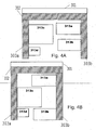
- FIG. 4A A different imager assembly is described in US 5,754,313 .
- two vertical members, 303a and 303b are used to support a horizontal member 302 on which the imaging sensor 301 is mounted.
- the electrical components 313a to 313d are mounted on the inner side of the vertical members 303.
- This assembly suffers from the same drawbacks described hereinabove with regard to Fig. 3A and it is mainly suitable in applications utilizing relatively large imaging sensors.
- the assembly shown in Fig. 4B illustrates how these drawbacks could be solved when the imaging sensor 301 utilized is of relatively small dimensions (approximately equal to, or smaller than 2 ⁇ 2 mm).
- the electrical components 313a to 313d are arranged in opposite directions on the inner sides of the vertical members 303. But since some of the components cannot be located directly opposite other components, because their combined length exceeds the limited space available, the electrical components must be mounted in a spaced apart arrangement as shown in Fig. 4B .
- the width of the imager corresponds to the dimensions of the imager sensor; however to achieve this result the length of the vertical members 303 must be increased over that of the design shown in Fig. 4A in order to provide the required space for all of the electrical components.
- the document JP2002131656 describes a camera design that is meant to reduce the size of an endoscopic camera. While this design may allow reducing the diameter of the camera over the other cameras available at the time, it is clear that there are aspects of the design which limit the degree of miniaturization that can be achieved. For example, it is clear from viewing the figures in the publication that the diameter of the camera head, i.e. of the package containing the CCD chip and the associated electronic circuitry, is greater than the diagonal dimension of the CCD chip.
- the present invention is directed towards an imager assembly for a miniature camera head.
- the basic preferred embodiment of the imager assembly of the invention comprises the following components:
- the conductive leads are bent and the circuitry and the conductive wires are arranged and mounted such that the dimensions of the camera head in the plane parallel to the sensor plane ("sensor plane” is defined throughout this document as the sensor's dimensions in the x ⁇ y plane (see Fig. 1 )) are approximately equal or less than the corresponding dimensions of the sensor.
- the circuitry is capable of delivering signals produced by the imaging sensor for further processing.
- the components of the imager, except for the imaging surface of the sensor and the objective lens system, are encapsulated by an isolating material.
- the electrical components of the circuitry are preferably lined-up behind the imaging sensor.
- the imaging sensor can be a CCD or a CMOS sensor. If it is a CCD, it can be part of a Tape Automated Bonding (TAB) imager package.
- TAB Tape Automated Bonding
- the circuitry includes amplification, resistive, capacitance, and conductive components for electrically linking the components of the circuitry.
- the amplification component can be an amplifier.
- the resistive components can be embedded into the conducting wires used for linking the circuitry components.
- burn-resistors are used.
- the electrical circuitry can further comprise a power source and a transmitter capable of wirelessly delivering the electrical signals produced by the circuitry and the imaging sensor to a remote location for processing. An internal power supply can be provided, making it unnecessary to provide power conductive wires to link the circuitry and the imaging sensor to an external power source.
- the circuitry may be an ASIC circuit and in a preferred embodiment the circuitry and the imaging sensor may be a single ASIC unit.
- the imager components, the encapsulating material, and the transmission lines have heat resistant characteristics enabling the imager to remain undamaged and the quality of the images it produces to be essentially unaffected by repeated autoclaving procedures.
- the present invention is directed towards an imaging system for processing and displaying the images that are acquired by the imager assembly of the invention.
- the system comprises:
- the display system can be capable of displaying images in VGA synchronization standard.
- the present invention provides an autoclavable imager assembly, having minimal size, which functions as a miniature camera head.
- the camera head of the invention comprises an imaging sensor, such as CCD, to acquire the images and the components required to process and amplify the attained signals and to deliver them via conductive wires to a display system that digitally processes the attained signals.
- CCD imaging sensor
- the quality of the image is greatly dependent on the number of electrical components that are mounted in the vicinity of the imager, to improve the signal quality.
- Electronic improvement is necessary because the signals that are transmitted via the conductive wires to the display system are distorted and attenuated by electrical noise and because of the presence of various other electrical effects, e.g., electrical resistance, along the conductive wires.
- the quality of the image also depends on many other factors including, but not limited to: the number of pixels in the imaging sensor, the amount of illumination (photon density) available, the amount of reflection from the target, environmental factors such as temperature of the cavity and residual temperature remaining in the camera head itself after the autoclaving process, and the activation procedure used for driving the imaging sensor.
- a small size CCD can be made to have the same signal strength as a larger one by increasing the illumination intensity, however this will result in increasing the overall size of the imager. This is because increased intensity is achieved by adding illumination means (fibers, diodes, etc). Therefore, in order to achieve small packaging of the imager without increasing the illumination means, special electronics-related methods are required to increase the signal strength and quality.
- the efforts to decrease the size of the imaging sensor require an increase in the number of components that need to be mounted near the imaging sensor in order to increase the gain and the resulting effect is an increase the overall volume of the package. This problem becomes more acute when the signal output from the CCD needs to travel along several meters of cable (for example, 5 to 15 meters) to the control processing unit without having any additional amplifiers between the attached CCD circuit and the control unit.
- the present invention solves these problems and provides effective assembly designs that enable the provision of high quality, stable images having reduced noise; while, at the same time, achieving small packaging size by utilizing a minimal number of electronic components.
- the main components required for delivering the image are an objective lens system (also referred to herein as an objective lens) located at the distal end of the imager assembly, an imaging sensor and a driver (amplifier) for operating the imaging sensor and delivering the image signals via the conductive wires.
- an objective lens system also referred to herein as an objective lens
- an imaging sensor located at the distal end of the imager assembly
- a driver amplifier
- Fig. 1 illustrates an imager assembly 111 .
- the components that are used to construct the imager 111 are assembled utilizing a layered configuration, in order to reduce the dimensions of the imager 111 to the minimum possible, namely the size defined by the sensor's dimensions in the sensor plane (referred to as the "sensor plane" throughout this application).
- the objective lens 100 is preferably of the same x ⁇ y dimensions as those of the sensor 101, or smaller, and is attached to the sensor's top (light receiving) face.
- the sensor 101 is attached to a horizontal plate 102, which is of the same x ⁇ y dimensions as those of the imaging sensor 101, or slightly smaller. As shown in Fig. 1 , all the layers used to assemble the imager 111 are attached in parallel and are spatially aligned.
- the electrical components (circuitry) 106 are mounted on the bottom surface of the horizontal plate 102.
- the electrical components 106 are connected to the imager leads 103 of the imaging sensor 101.
- the leads are vertically bent back towards the bottom surface of plate 102 via circular grooves 104 which are formed on opposite sides of the plate 102.
- the imager leads are linked to the circuitry 106 via connection points 105 located on the bottom surface of the horizontal plate 102, preferably by soldering.
- the signal transmission and electrical supply wires 108 of the cable 107 are also linked to the circuitry 106 via connection points 118 located on the bottom surface of the horizontal plate 102, which also serves as a PCB.
- the plate 102 is a ceramic PCB or special polymer (for example, Teflon) plate that withstands high temperature and has a thermo expansion coefficient similar to that of the sensor.
- the circuitry 106 is printed on the bottom surface of the plate.
- the circuitry 106 preferably includes an amplifying component (not shown), which is required for driving the imaging sensor 101.
- An N-channel field effect transistor (FET) is usually used as the amplifying element in such designs.
- the amplifying element is implemented by an amplifier circuit such as a Maxim operational amplifier that includes several amplifying stages.
- the resistive components (not shown) of the circuitry 106 are implemented by utilizing burn-resistors.
- the burn-resistors are embodied in the PCB conducting lines, and serve as electrical links between the electrical components. In this way the space consumed by the resistive components essentially becomes negligible. The space saved in this manner may be exploited either to reduce the amount of space consumed by the circuitry 106 or, alternatively, for introducing additional electrical components to improve the quality of the transmitted signal.
- the overall length of the imager 111 is the sum of the thicknesses/lengths of the various layers: d1 of the objective lens 100, d2 of the imaging sensor 101, d3 of the horizontal plate 102, and d4, the length of the electrical components 106.
- the thickness of the objective lens 100 is ⁇ 1.4 mm
- the thickness of the imaging sensor 101 is ⁇ 0.65mm, including the glass cover (e.g., Sony ICX257FKW or ICX256FKW CCD) image sensors)
- the thickness of the plate 102 is preferably ⁇ 0.15mm (it can be 0.08mm or less)
- the length of the gap d4 is preferably ⁇ 1.1mm.
- the dimensions (x ⁇ y) of the imaging sensor (in the horizontal plate) are preferably ⁇ 2 ⁇ 2mm, or smaller.
- the tips of the bent imager leads 103 add ⁇ 0.1mm to the length in the x dimension of the imaging sensor 101, which results in dimensions in the sensor plane of the imager of about 2.2 ⁇ 2mm, or less.
- the imager assembly 111 is encapsulated by an isolating material, preferably non-conductive epoxy glue, which has a temperature resistance high enough to maintain the integrity of the imager 111 and its electronic components both in the operating environment and also under sterilizing conditions, for example, autoclave sterilization at 134°C and pressure of 2.3bar.
- the imaging sensor 101 is preferably a type of TAB CCD imager and, in this case, the protective strips 120 of the TAB imager packaging are preferably bonded to the bottom side of the horizontal plate 102.
- Fig. 2 illustrates two parallel horizontal plates 102 and 207 which are used for mounting the imaging sensor 101 and the electrical components 206.
- the imager assembly 222 shown in Fig. 2 is also arranged in a layered configuration.
- the objective lens 100 is attached to the imaging sensor 101.
- the imaging sensor is in turn, attached to the top surface of the first horizontal plate 102, which is of the same x ⁇ y dimensions as those of the imaging sensor 101, or slightly smaller.
- a second horizontal plate 207 is situated parallel to horizontal plate 102, forming a gap of length d5 with the first plate 102.
- the electronic circuitry 206 is connected to the imager leads 103, which are vertically bent back towards the bottom surface of the horizontal plate 102 via the circular grooves 104.
- a portion of the electrical components (circuitry) 206 is mounted on the bottom surface of the first horizontal plate 102, and another portion of this circuitry 206 is mounted on the top surface of the second horizontal parallel plate 207.
- the transmission and electric supply wires 200 which are attached to contact points 201 on the bottom surface of the first horizontal plate 102, and to the contact points 202 on the top surface of the second parallel plate 207, are used to connect the two portions of circuitry 206.
- This preferred embodiment of the invention occupies a larger volume of space than the embodiment shown in Fig. 1 , however the circuitry 206 used to drive the imaging sensor 101 can be designed to include more components than the corresponding circuit 106.
- the additional components are used to give this embodiment, for example, the ability to transmit both digital and analog signals over long distances (greater than five meters) or to transmit wireless signals.
- the signal transmission and electrical supply wires 108 of the cable 107 are attached to the bottom surface of the second horizontal plate 207, and connected to the circuitry 206 via conduction paths 118 located within the second parallel plate 207. In this assembly, some of the wires 108 pass through bores in the second horizontal plate 207 and are directly linked to the imager leads 103 of the imaging sensor 101 and/or to the circuitry portion mounted on the first horizontal plate 102, via contact points 201.
- the signal transmission and electrical supply wires 108 of the cable 107 are preferably bent vertically into the spatial plane of plate 207, such that they are attached to the bottom surface of the second horizontal plate 207 in their fully exposed length.
- the tip of the cable 117 is actually tightly attached to the second parallel plate 207, which further minimizes the length of the rigid portion of the imager 222 and reduces the rigid segment of the signal transmission and electrical supply wires 108 to a negligible length of about ⁇ 0.1mm.
- the overall rigid length of the imager 222 is obtained by the summation of the thicknesses d1 ( ⁇ 1.4mm) of the objective lens 100, d2 ( ⁇ 0.65mm) of the imaging sensor 101, 2 *d3 ( ⁇ 0.3mm) of the first and second parallel plates 102 and 207, and d5 ( ⁇ 2.35mm) of the distance between the parallel plates, thus obtaining physical dimensions of about ⁇ 2.2 ⁇ 2 ⁇ 4.7mm.
- additional plate layers can be added in parallel beneath the second horizontal plate 207, if required, according to the design needs.
- additional conductive wires 200 must be used to electrically link them, and the wires of the cable 107 will preferably be connected to the bottom surface of the last parallel plate and extend through bores in the plates towards the imager leads 103 of the imaging sensor 101.
- electrical circuitry may be mounted on both sides of the additional parallel plates.
- the circuitries 106, 206, of the preferred embodiments of the invention are preferably mounted on the horizontal plates utilizing state-of-the-art techniques.
- the circuitry can be mounted by building the circuitry interconnections on the plates or by grooves and having its components (conductors, resistors, etc.) screen-printed onto the plates, utilizing various film technologies.
- the resistors (not shown) are preferably burn-resistors.
- the thickness of the ceramic plates (102 and 207) is preferably ⁇ 0.15mm and can be even smaller, such as 0.08mm, and the imager assemblies 111, 222 (with the exception of the objective lens and imaging sensor) are encapsulated by an isolating material with an appropriate thermal expansion coefficient (e.g., nonconductive epoxy glue, ceramic, or a polymer formula such as nonconductive Teflon, or PTFE).
- an isolating material with an appropriate thermal expansion coefficient e.g., nonconductive epoxy glue, ceramic, or a polymer formula such as nonconductive Teflon, or PTFE.
- the imager components used preferably have temperature resistance to provide the imager with the ability to withstand sterilization temperatures achieved in procedures such as autoclaving.
- the imaging sensor can be from the Sony ICX257/6 family that are heat proof to ⁇ 155°C and the ceramic plate used can be a Coors Ceramic Company AD-96 type which is heat proof to ⁇ 800°C.
- the encapsulation material is preferably heat proof to ⁇ 300°C.
- Capacitance elements are preferably types of VISHAY 100nF, which are heat proof to ⁇ 210°C.
- the circuitry which can be manufactured utilizing ceramic techniques, can have immunity to heat up to ⁇ 380°C, and the circuitry conducting paths are preferably made of gold.
- Several types of objective lens, such as KF9, which are heat proof to ⁇ 200°C, can be used.
- the signal transmission and power supply wires and cable are preferably able to withstand temperatures of at least ⁇ 210°C.
- an isolating material is preferably used to encapsulate the imager components.
- the encapsulating material provides sealing properties enabling the imager assembly to withstand repeated autoclaving procedures.
- the transparent adhesive used to attach the objective lens system to the CCD is capable of withstanding the autoclave temperature and has a thermal expansion coefficient that prevents temperature impacts, resulting from the autoclave temperature that may damage the imager construction.
- Distortion of the imaging sensor signal may appear as a result of heating during the autoclaving process or as a result of working in a hot environment, such as a turbine engine.
- the two major types of distortions are of the spatial resolution and deviations from the Small Signal Approximation (around a working point), which is usually used to design the electronics. These distortions are minimized by utilizing electronic corrections, for instance doubling the acquiring image frequency, as will be discussed hereinbelow.
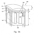
- Figs. 5A , 5B , 6A , and 6B illustrate imager assemblies (555 and 666) wherein the volume occupied by the imager is further reduced.
- These designs are preferably used for especially small imaging sensors (e.g., ⁇ 2 ⁇ 2mm or smaller).
- the general approach used in these designs is to mount the electrical circuitry 106 under the imaging sensor 101 without using plates (PCBs) as in the previously discussed embodiments.
- the imager leads 103 (and the protective strips 120, if a type of TAB imager packaging is used) are bent downwards in the vertical direction from the imaging sensor x ⁇ y plane.
- the components of the electrical circuitry 106 are connected directly according to the circuitry requirements, utilizing conductive wires 502, preferably by soldering and/or conductive glue and/or sonic soldering.
- some of the transmission and electrical supply wires 108 are connected directly to the imager leads 103 and some of the wires 108 and the imager leads 103, may be connected directly to the electrical components of circuitry 106, preferably by soldering and/or conductive glue and/or sonic soldering.
- All of the imager components except the objective lens system and the sensor's light receiving aperture are encapsulated utilizing an isolating material 500, preferably a type of a ceramic or non-conductive polymer material.
- the encapsulating material 500 is used to attach the electrical circuitry 106, the wires 108, and the imager leads 103 to the bottom side of the imaging sensor 101, and to provide the heat and pressure resistance required for protecting these components in autoclaving procedures.
- the dimensions of the imager are therefore reduced to the dimension of the imaging sensor (in the sensor plane), and the thickness of the lens d1 , imaging sensor d2, and the length d5 of the encapsulated portion (in the direction perpendicular to the sensor plane), i.e. x ⁇ y ⁇ ( d 1+ d 2+ d5 )mm.
- Fig. 5B demonstrates a possible way of encapsulating the imager assembly 555.
- a mold 505 is preferably used for molding the isolating material used for encapsulating the imager components.
- the mold is preferably a plastic mold (e.g., made of Teflon or similar material), which preferably has inner dimensions equivalent to the dimensions in the sensor plane of the imaging sensor 101, or slightly larger.
- the imager assembly is held inverted and the mold 505 is positioned on the bottom of the imaging sensor such that almost all the imager components are enclosed within the mold 505.
- the sensing surface of the imager is left outside the mold 505.
- the tips of the imager leads 103 can also be preferably enclosed in the mold.
- the isolating material 500 is poured into the volume enclosed within the mold 505 and, once it hardens, the mold can be removed. After removal of the mold, the lens is attached to the sensing surface of the imager using a suitable transparent adhesive.
- the imager assembly illustrated in Fig. 6A demonstrates another possible assembly, wherein all the electrical components of the circuitry 106 are placed in line, one after the other, behind the imaging sensor 101.
- This approach is particularly favorable in, but not limited to, implementations utilizing imaging sensors having physical dimensions of 1 ⁇ 1mm, or smaller.
- This design is also advantageous in that it allows using electrical components which are larger in volume, but which are preferably not wider than the dimensions of the imaging sensor in the sensor plane.
- This approach affects the length of the imager, which may be elongated due to the lining of the imager inner components.
- this disadvantage can be alleviated by encapsulating the imager components utilizing a flexible isolating material (500). In this way the disadvantage of the elongated length of the imager 666 is eliminated, in particular when a very small imaging sensor is used, as intended in this design.
- Fig. 6B shows an embodiment similar to that of Fig. 6A , but requiring less space.
- all of the various circuit elements are incorporated into a single ASIC circuit 106.
- This embodiment can be even further reduced in size by incorporating the imaging sensor 101 and the electronic components of the circuitry 106 into a single ASIC unit.
- Fig. 7 illustrates a possible embodiment of the circuitry 106 (206) of the invention.
- the imaging sensor is preferably a SONY ICX256/7FKW CCD (other cameras or CCDs that could be used are, for example, Panasonic camera GP-KS2MMH/ES1, based on 1/10" CCD and Sanyo LC99267FSB 1/9" CCD).
- the amplifier 700 is preferably a Maxim operational amplifier.
- the resistive components R1 and R2 are preferably a type of burn-resistor that are embedded into the conducting links (preferably gold wires) connecting the electrical components of the circuitry 106 (206), and which resistances are preferably 500 ⁇ and 50 ⁇ respectively.
- the capacitors C1 and C2 are both preferably 100nF (25v).
- the wires are industrial type 12-wire AWG #38 wires.
- circuitries 106 and 206 can include an independent power supply and a radio transmitter for transmitting the image signals received by the circuitry. Obviously, in such wireless implementations there is no need to link the imager via transmission and power supply wires.
- the imaging sensor is preferably a type of a CCD sensor and thus the discussion hereinbelow specifically relates to this type of sensor, and particularly to the SONY ICX256/7FKW CCD family.
- the dynamic response of the CCD camera is significantly improved, in comparison with the PAL/NTSC standards, which are used in the majority of similar implementations.
- the preferred embodiment of the CCD camera is described hereinafter with reference to the PAL standard, although similar embodiments applying to the NTSC standard can also be used.
- the field acquisition rate is doubled, by increasing the pixel acquisition rate.
- This is preferably carried out by utilizing special discrete analog horizontal phase drivers and ultra fast analog signal processing circuits (e.g., double correlated sampling).
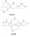
- Fig. 9A illustrates a possible implementation of a discrete analog horizontal phase driver that can be used to generate the signal required for operating the CCD sensor.
- a Wideband Phase Driver 903 is utilized for generating the signals, in accordance with the signals received from the Digital Generator 902 and the offsets provided via the Offset Adjustment 901.
- the Wideband Phase Driver 903 amplifies the generated signal and outputs it via the Bias Circuit 904, the output of which is used to for driving the CCD sensor. It should be noted that it is possible to use other signal multiplication means to increase the field rate.
- Fig. 9B exemplifies a possible implementation of a double correlated sampler that can be used for the analog signal processing of the signal received from the imager.
- the output ( Fig. 7 ) signal from Pre-amplifier 910 is fed into two Sample and Hold units, (Signal Sample & Hold unit 912 and Reference Level Sample & Hold unit 911), which are used to extract two signal levels of the outputted signal that are needed for determining a single pixel.
- the intensity of the acquired pixel is provided by the output of the Differential Stage 913, which provides the signal difference between the two signal levels provided by the Sample and Hold units, 911 and 912.
- the VGA video standard is preferably used for the display, since it is capable of providing a frame refresh rate that is four times higher than that of the PAL standard.
- the outputted display is progressive, which improves the image provided and prevents flickering on the display screen.
- the design of the vertical timing enables the separation between fields during the readout process.
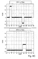
- the voltage pattern VI-V4 is used to retrieve even and odd line fields ( f1 , f2, f3 ,..., f100 ).
- the quality and stability of the acquired image is substantially improved. This can be seen, for example, when comparing to the PAL/NTSC interlaced standards, in which 50 fields are acquired per second, where each field consists of half the number of lines actually available in the sensor, due to line summation.
- each field is extracted separately (only one phase appears in each field) as shown in Fig. 8D for V1 (odd field signal) and V3 (even field signal), thus field summation is not performed and the outputted image is actually made up of the full number of pixels that are practically available to the imaging sensor.
- the exact vertical timing of the readout process is illustrated for the odd field in waveforms "V1 and V2, Odd Field Readout” in Fig. 8A , "V1 and V3, Odd Field Readout” in Fig. 8B , and "V1 and V4, Odd Field Readout” in Fig. 8C .
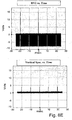
- Fig. 8F shows the waveform obtained on the "CCD's Output", which has a period of 40nsec. Obviously, this output signal (25 M pixels/see) is a substantial improvement over that obtained by use of the traditional PAL standard (9.5 M pixels/sec) for the spatial resolution of these CCDs.
- the vertical synchronization signal shown in Fig. 8E determines the display rate on screen.
- the time difference between two adjacent frame synchronizations signal ( ⁇ 4 volt pulse) is 10 msec (100 Hz).
- Table 1 Video Solutions Based on ICX257FKW Feature Standard use (PAL) Nonstandard use (Present Invention) Acquisition Rate From CCD 50 fields/sec 100 fields/sec Field Summation During CCD Readout Exists (the CCD's output always contains the sum of 2 adjacent lines) None (each line is separately extracted from the CCD) Pixel Acquisition Rate 9.5 M pixels/sec (For the current spatial resolution) 25 M pixels/sec Display Rate On Screen 50 fields/sec 100 fields/sec Synchronization Standard on Screen Y/C VGA Display Mode Interlaced Progressive
Landscapes
- Engineering & Computer Science (AREA)
- Multimedia (AREA)
- Signal Processing (AREA)
- Health & Medical Sciences (AREA)
- Life Sciences & Earth Sciences (AREA)
- Surgery (AREA)
- Radiology & Medical Imaging (AREA)
- Molecular Biology (AREA)
- Optics & Photonics (AREA)
- Pathology (AREA)
- Biophysics (AREA)
- Physics & Mathematics (AREA)
- Biomedical Technology (AREA)
- Heart & Thoracic Surgery (AREA)
- Medical Informatics (AREA)
- Nuclear Medicine, Radiotherapy & Molecular Imaging (AREA)
- Animal Behavior & Ethology (AREA)
- General Health & Medical Sciences (AREA)
- Public Health (AREA)
- Veterinary Medicine (AREA)
- Solid State Image Pick-Up Elements (AREA)
- Transforming Light Signals Into Electric Signals (AREA)
- Studio Devices (AREA)
Description
- The present invention relates to the field of endoscopy and imaging systems used in minimal access therapy and/or diagnostics. More particularly, the invention relates to arrangements of a miniature camera head allowing compact arrangement of the components of the camera head.
- The present invention is directed to imager assemblies for miniature camera heads based on solid state sensors e.g., Charged Couple Device (CCD) sensors. These types of cameras are commonly used in imaging systems in minimal access therapy e.g., minimal access surgery, interventional flexible endoscopy, percutaneous interventional radiology, laparoscopy, etc.
- Minimal access therapy and/or diagnostics are generally carried out within body cavities and, therefore, the operating field cannot be directly viewed by the person carrying out the operation. For this reason, the ability to carry out such procedures is dependent on the imaging systems that display the images obtained by the camera sensor focused on the scene of the operation. The imaging systems are usually divided into rigid types of devices (such as laparoscopes) and flexible types of devices (flexible endoscopes). Many of the rigid type devices that are commonly used, known as telescopes, are based on the Hopkins rod-lens system. These devices allow the operator to gain an inner view of the operative field for diagnostics and dissection. The flexible devices that are commonly used are usually based on fiber optic telescopes. These types of flexible endoscopes utilize fiber optics to transmit light into the operative field, and to transfer the image of the operative field to the endoscope eyepiece.
- Another type of device that is widely adopted, known as the chip-on-stick technology, is based on optoelectronic instruments. In these devices, an imaging sensor (e.g., CCD) is usually used at the distal end of the telescope or flexible endoscope to record the images produced by an objective lens. Most of the modern miniature cameras that are used in minimal access therapy are of the chip-on-stick variety based on CCD sensors (examples of commercially available devices of this kind are the EndoEYE™ Surgical Videoscopes by Olympus). The optoelectronic systems provide improved image quality and greater light and image sensitivity than the formerly mentioned solutions. However, their performance is affected by the amount of light available in the endoscope, which is dependent upon the size of the illumination means such as the fibers used to transmit the light from a remote source to the operating area, or the Light Emitting Diodes (LEDs) used.to illuminate the cavity, e.g., stomach, colon, etc.
- The operation of solid state imaging sensors is based on conversion of photons striking the sensor into electron charges (known as the photoelectric effect). The output of the sensor is an electric current, or voltage. The voltage, which is proportional to the number of photons that strike each pixel of the sensor, is amplified by an amplifying device. The amplified signal is usually further processed by converting the voltage signals obtained from the amplifier into equivalent digital signals. Solid-state sensors are utilized to provide images characterized by high-quality and reduced noise levels.
- Most chip-on-stick instruments are sensitive to non-chemical sterilization procedures such as autoclaving of the optical components of the imager assembly. This sensitivity results from several causes, one being that the imaging sensor, the objective lens system, and other components of the imager are usually encapsulated utilizing transparent adhesive materials that may lose their transparency as a result of the temperature and pressure involved in the autoclaving process. The loss of transparency is accompanied by a substantial deterioration of the optical qualities of the imager. Another cause of the sensitivity is problems caused by leakage resulting from the pressure of the steam involved in autoclaving.
- Additionally, signal distortions result, during medical and industrial procedures, when the environment is hot in comparison to the room temperature or due to residual heat after the autoclaving procedure. It is possible that some of these problems can be overcome by arranging the imager components in a spaced construction utilizing a dedicated enclosure and fastening elements, as described in
US 6,019,719 . However, although this spaced construction resolves the autoclaving drawbacks discussed above, it also substantially enlarges the imager dimensions. Thus it is not a viable solution when it is necessary to include miniature electrical circuitry in the vicinity of the imaging sensor, as is the case in applications utilizing relatively small imaging sensors. - There is an ongoing effort to reduce the dimensions of the camera heads used in optoelectronic instruments, in order to provide improved penetration and access to bodily organs, e.g., to the lower layer of the lung or deep into the kidney, brain, etc. One of the difficulties that must be solved in designing increasingly smaller camera heads is that the density of photons received by the imaging sensor becomes limited by the sensor's small dimensions. Additionally, the amount of light illuminating the scene is small since the source of illumination (e.g.; fiber, LED, or the like) must also be kept very small. Therefore, the signal received from the imaging sensor has to be amplified requiring the use of additional electrical components that are preferably mounted in the vicinity of the imaging sensor. Use of these additional electrical components increases the complexity of the camera heads and multiplies the difficulties in creating miniature and autoclavable imager designs.
- An imager assembly is described in
US 5,857,963 , in which the imaging sensor is mounted on a T-shaped support member 300a, as shown inFig. 3A . In this assembly theimaging sensor 301 is located in a recess formed on thehorizontal member 300b.Circuitry components 313a to 313d, for driving theimaging sensor 301, are mounted on thevertical member 300a. This assembly is beneficial in applications utilizing imaging sensors of relatively large dimensions (e.g., 1/6" or 1/4" CCDs), wherein all theelectrical components 313a to 313d can be compactly arranged on thevertical member 300a without affecting the overall dimensions of the imager assembly. - However, if the imaging, sensor used is of relatively small dimensions (e.g., ∼2×2 mm or less), the imager assembly design requires careful consideration of the lengths of the
electrical components 313a to 313d. It can be seen that the dimensions of the imager assembly shown inFig. 3A (in a plane parallel to the plane of the sensor) can be reduced by mounting the imaging sensor on a horizontal member which has same, or smaller, dimensions as those of theimaging sensor 301, as shown inFig. 3B . Since the lengths of theelectrical components 313a to 313d are typically about 1mm, in applications utilizing imaging sensors approximately equal to, or smaller than, 2×2 mm, the edges of the electrical components will project beyond the virtual edges e1 and e2 defined by the dimensions in the plane of theimaging sensor 301. In this case, the dimensions in the plane parallel to the plane of the sensor of the imager assembly are determined by the thickness of thevertical member 300a and the length of theelectrical components 313a to 313d. - A different imager assembly is described in
US 5,754,313 . As shown inFig. 4A , in this assembly two vertical members, 303a and 303b, are used to support ahorizontal member 302 on which theimaging sensor 301 is mounted. Theelectrical components 313a to 313d are mounted on the inner side of the vertical members 303. This assembly suffers from the same drawbacks described hereinabove with regard toFig. 3A and it is mainly suitable in applications utilizing relatively large imaging sensors. - The assembly shown in
Fig. 4B illustrates how these drawbacks could be solved when theimaging sensor 301 utilized is of relatively small dimensions (approximately equal to, or smaller than 2×2 mm). In the assembly shown inFig. 4B , theelectrical components 313a to 313d are arranged in opposite directions on the inner sides of the vertical members 303. But since some of the components cannot be located directly opposite other components, because their combined length exceeds the limited space available, the electrical components must be mounted in a spaced apart arrangement as shown inFig. 4B . In the arrangement shown inFig. 4B the width of the imager corresponds to the dimensions of the imager sensor; however to achieve this result the length of the vertical members 303 must be increased over that of the design shown inFig. 4A in order to provide the required space for all of the electrical components. - In the imager assembly described in
US 6,142,930 a different design approach is used. In this assembly the electrical components are mounted on a circuit board positioned behind the imaging sensor. Since this imager is designed to be installed in a shielded pipe, reinforcing plates are required to support the imager, and the imaging sensor leads are bent into an L-shape in order to connect them to the bottom side of the circuit board. This design requires less space than the abovementioned designs, however it is far from optimal as far as miniaturization is concerned and must be improved upon to accommodate the required circuitry and imaging sensors of relatively small dimensions (e.g., to fit into a package having a cross-section of less than or approximately equal to 2×2 mm and having a very short length). The design is not optimal since the CCD is supported by an external housing; the electrical components are placed on a plate within the housing, spaced apart from the CCD; and because of the presence of a separate reinforcement plate for a flexible circuit board. - A similar approach is also used in
patent application JP 2001037713A2 - The document
JP2002131656 - The methods described above do not provide a satisfactory solution to the problem of minimizing the dimensions of imager assemblies that comprise an imaging sensor of relatively small dimensions. The prior art assemblies also fail to provide miniature imager assemblies utilizing very small imaging sensors that maintain their optical qualities even after being repeatedly sterilized utilizing autoclaving procedures.
- It is an object of the present invention to provide an imager assembly utilizing an imaging sensor of relatively small dimensions having efficient and minimal packaging confined by the dimensions, of the imaging sensor.
- It is another object of the present invention to provide an imager assembly that can be efficiently sterilized utilizing autoclaving sterilization procedures.
- It is a further object of the present invention to provide an imager assembly having minimal dimensions and improved flexibility enabling it to be utilized with very small diameter endoscopes.
- It is a still further object of the present invention to provide an imager assembly and related electronics comprising means to overcome problems caused by the miniaturization process, e.g., means of reducing the electrical noise, flicker, etc.
- It is yet another object of the present invention to provide an imager assembly utilizing an imaging sensor of relatively small dimensions having efficient and minimal packaging and providing high quality and stable images under conditions of relatively low levels of illumination.
- Other objects and advantages of the invention will become apparent as the description proceeds.
- In a first aspect the present invention is directed towards an imager assembly for a miniature camera head. The basic preferred embodiment of the imager assembly of the invention comprises the following components:
- a) an imaging sensor having conductive leads emanating from two opposite sides of the sensor, for outputting and/or inputting electric signals and/or power;
- b) an objective lens system placed on top of the sensor;
- c) circuitry, mounted beneath the imaging sensor, for driving the sensor and amplifying the electrical signals; the components of the circuitry are electrically linked, according to the circuit requirements, to each other and to the sensor leads by conductive wires;
- d) conductive wires electrically linked to the circuitry and to the leads of the imaging sensor for conducting electrical signals between the electrical circuitry and a remote location; and
- e) conductive wires electrically linked to the circuitry and to the leads of the imaging sensor to provide them with electrical power from an external power supply.
- The conductive leads are bent and the circuitry and the conductive wires are arranged and mounted such that the dimensions of the camera head in the plane parallel to the sensor plane ("sensor plane" is defined throughout this document as the sensor's dimensions in the x×y plane (see
Fig. 1 )) are approximately equal or less than the corresponding dimensions of the sensor. The circuitry is capable of delivering signals produced by the imaging sensor for further processing. The components of the imager, except for the imaging surface of the sensor and the objective lens system, are encapsulated by an isolating material. The electrical components of the circuitry are preferably lined-up behind the imaging sensor. - The imaging sensor can be a CCD or a CMOS sensor. If it is a CCD, it can be part of a Tape Automated Bonding (TAB) imager package.
- The circuitry includes amplification, resistive, capacitance, and conductive components for electrically linking the components of the circuitry. The amplification component can be an amplifier. The resistive components can be embedded into the conducting wires used for linking the circuitry components. Preferably, burn-resistors are used. The electrical circuitry can further comprise a power source and a transmitter capable of wirelessly delivering the electrical signals produced by the circuitry and the imaging sensor to a remote location for processing. An internal power supply can be provided, making it unnecessary to provide power conductive wires to link the circuitry and the imaging sensor to an external power source. The circuitry may be an ASIC circuit and in a preferred embodiment the circuitry and the imaging sensor may be a single ASIC unit.
- The imager components, the encapsulating material, and the transmission lines have heat resistant characteristics enabling the imager to remain undamaged and the quality of the images it produces to be essentially unaffected by repeated autoclaving procedures.
- In another aspect, the present invention is directed towards an imaging system for processing and displaying the images that are acquired by the imager assembly of the invention. The system comprises:
- a) a signal generator capable of providing voltage signals via the conductive wires for driving the imaging sensor to obtain acquisition rates of at least 100 fields per second;
- b) circuitry for separately extracting each line of the acquired fields that are received from the imager;
- c) circuitry for outputting a continuous display rate of at least 100 full-frames per second by combining the lines of the previously read field with the lines of the currently read fields; and
- d) a display system capable of displaying the outputted image in a continuous and non-interlaced mode, wherein the circuitry for extracting each line of the acquired fields separately prevents line summation during field readout thereby improving image quality and the dynamic response obtained by the imaging sensor.
- According to the imaging system of the invention, the display system can be capable of displaying images in VGA synchronization standard.
- All the above and other characteristics and advantages of the invention will be further understood through the following illustrative and non-limitative description of preferred embodiments thereof, with reference to the appended drawings.
-
-
Fig. 1 illustrates an imager assembly utilizing a single parallel plate; -
Fig. 2 illustrates an imager assembly utilizing a pair of parallel plates ; -
Figs. 3A and 3B illustrate a side view of an imager assembly utilizing a T-shaped member support; -
Figs. 4A and 4B illustrate a side view of an imager assembly utilizing two vertical support members -
Figs. 5A ,5B ,6A , and6B illustrate imager assemblies of the invention in which the electrical circuitry is not mounted on PCBs; -
Fig. 7 schematically illustrates a preferred embodiment of the electrical circuitry of the invention; -
Figs. 8A-8F are voltage graphs illustrating the electrical operation of the imager according to a preferred embodiment of the invention; -
Fig. 9A is a block diagram illustrating a discrete analog horizontal phase drive; and -
Fig. 9B is a block diagram illustrating an ultra fast analog signal processing circuitry. - The present invention provides an autoclavable imager assembly, having minimal size, which functions as a miniature camera head. The camera head of the invention comprises an imaging sensor, such as CCD, to acquire the images and the components required to process and amplify the attained signals and to deliver them via conductive wires to a display system that digitally processes the attained signals. As explained hereinbelow, the quality of the image is greatly dependent on the number of electrical components that are mounted in the vicinity of the imager, to improve the signal quality. Electronic improvement is necessary because the signals that are transmitted via the conductive wires to the display system are distorted and attenuated by electrical noise and because of the presence of various other electrical effects, e.g., electrical resistance, along the conductive wires. The quality of the image also depends on many other factors including, but not limited to: the number of pixels in the imaging sensor, the amount of illumination (photon density) available, the amount of reflection from the target, environmental factors such as temperature of the cavity and residual temperature remaining in the camera head itself after the autoclaving process, and the activation procedure used for driving the imaging sensor.
- There is a clear relationship between the physical dimensions of an instrument containing a miniature imaging-sensor having a certain number of pixels, and the amount of illumination needed to obtain a bright image. For example, a CCD with 480,000 pixels (1/6" CCD) requires a light source (xenon, halogen, LED, etc.) having a given intensity, while a smaller CCD (for example, a "1/10" CCD) with 300,000 pixels requires more light in order to present an image of similar quality. In the smaller-size CCD, the strength of the signals is less than for the larger CCD because the total number of photons received by the imaging sensor is substantially lower. A small size CCD can be made to have the same signal strength as a larger one by increasing the illumination intensity, however this will result in increasing the overall size of the imager. This is because increased intensity is achieved by adding illumination means (fibers, diodes, etc). Therefore, in order to achieve small packaging of the imager without increasing the illumination means, special electronics-related methods are required to increase the signal strength and quality. Thus the efforts to decrease the size of the imaging sensor require an increase in the number of components that need to be mounted near the imaging sensor in order to increase the gain and the resulting effect is an increase the overall volume of the package. This problem becomes more acute when the signal output from the CCD needs to travel along several meters of cable (for example, 5 to 15 meters) to the control processing unit without having any additional amplifiers between the attached CCD circuit and the control unit.
- The present invention solves these problems and provides effective assembly designs that enable the provision of high quality, stable images having reduced noise; while, at the same time, achieving small packaging size by utilizing a minimal number of electronic components.
- The main components required for delivering the image are an objective lens system (also referred to herein as an objective lens) located at the distal end of the imager assembly, an imaging sensor and a driver (amplifier) for operating the imaging sensor and delivering the image signals via the conductive wires.
-
Fig. 1 illustrates animager assembly 111 . The components that are used to construct theimager 111 are assembled utilizing a layered configuration, in order to reduce the dimensions of theimager 111 to the minimum possible, namely the size defined by the sensor's dimensions in the sensor plane (referred to as the "sensor plane" throughout this application). Theobjective lens 100 is preferably of the same x×y dimensions as those of thesensor 101, or smaller, and is attached to the sensor's top (light receiving) face. Thesensor 101 is attached to ahorizontal plate 102, which is of the same x×y dimensions as those of theimaging sensor 101, or slightly smaller. As shown inFig. 1 , all the layers used to assemble theimager 111 are attached in parallel and are spatially aligned. - The electrical components (circuitry) 106 are mounted on the bottom surface of the
horizontal plate 102. Theelectrical components 106 are connected to the imager leads 103 of theimaging sensor 101. The leads are vertically bent back towards the bottom surface ofplate 102 viacircular grooves 104 which are formed on opposite sides of theplate 102. The imager leads are linked to thecircuitry 106 via connection points 105 located on the bottom surface of thehorizontal plate 102, preferably by soldering. The signal transmission andelectrical supply wires 108 of thecable 107 are also linked to thecircuitry 106 via connection points 118 located on the bottom surface of thehorizontal plate 102, which also serves as a PCB. - The
plate 102 is a ceramic PCB or special polymer (for example, Teflon) plate that withstands high temperature and has a thermo expansion coefficient similar to that of the sensor. Thecircuitry 106 is printed on the bottom surface of the plate. Thecircuitry 106 preferably includes an amplifying component (not shown), which is required for driving theimaging sensor 101. An N-channel field effect transistor (FET) is usually used as the amplifying element in such designs. In a preferred embodiment of the invention, the amplifying element is implemented by an amplifier circuit such as a Maxim operational amplifier that includes several amplifying stages. In order to reduce the physical dimensions of thecircuitry 106, the resistive components (not shown) of thecircuitry 106 are implemented by utilizing burn-resistors. The burn-resistors are embodied in the PCB conducting lines, and serve as electrical links between the electrical components. In this way the space consumed by the resistive components essentially becomes negligible. The space saved in this manner may be exploited either to reduce the amount of space consumed by thecircuitry 106 or, alternatively, for introducing additional electrical components to improve the quality of the transmitted signal. - As shown in
Fig. 1 , the overall length of theimager 111 is the sum of the thicknesses/lengths of the various layers: d1 of theobjective lens 100, d2 of theimaging sensor 101, d3 of thehorizontal plate 102, and d4, the length of theelectrical components 106. According to one preferred embodiment of the invention the thickness of theobjective lens 100 is ∼1.4 mm, the thickness of theimaging sensor 101 is ∼0.65mm, including the glass cover (e.g., Sony ICX257FKW or ICX256FKW CCD) image sensors), the thickness of theplate 102 is preferably ∼0.15mm (it can be 0.08mm or less), and the length of the gap d4 is preferably ∼1.1mm. The dimensions (x×y) of the imaging sensor (in the horizontal plate) are preferably ∼2×2mm, or smaller. The tips of the bent imager leads 103 add ∼0.1mm to the length in the x dimension of theimaging sensor 101, which results in dimensions in the sensor plane of the imager of about 2.2∼2mm, or less. - With this assembly, the overall dimensions of the
imager 111 are about 2.2×2×3.3mm. Theimager assembly 111 is encapsulated by an isolating material, preferably non-conductive epoxy glue, which has a temperature resistance high enough to maintain the integrity of theimager 111 and its electronic components both in the operating environment and also under sterilizing conditions, for example, autoclave sterilization at 134°C and pressure of 2.3bar. Theimaging sensor 101 is preferably a type of TAB CCD imager and, in this case, theprotective strips 120 of the TAB imager packaging are preferably bonded to the bottom side of thehorizontal plate 102. -
Fig. 2 illustrates two parallelhorizontal plates imaging sensor 101 and theelectrical components 206. Theimager assembly 222 shown inFig. 2 is also arranged in a layered configuration. Theobjective lens 100 is attached to theimaging sensor 101. The imaging sensor is in turn, attached to the top surface of the firsthorizontal plate 102, which is of the same x×y dimensions as those of theimaging sensor 101, or slightly smaller. A secondhorizontal plate 207 is situated parallel tohorizontal plate 102, forming a gap of length d5 with thefirst plate 102. Theelectronic circuitry 206 is connected to the imager leads 103, which are vertically bent back towards the bottom surface of thehorizontal plate 102 via thecircular grooves 104. - A portion of the electrical components (circuitry) 206 is mounted on the bottom surface of the first
horizontal plate 102, and another portion of thiscircuitry 206 is mounted on the top surface of the second horizontalparallel plate 207. The transmission andelectric supply wires 200 which are attached to contactpoints 201 on the bottom surface of the firsthorizontal plate 102, and to the contact points 202 on the top surface of the secondparallel plate 207, are used to connect the two portions ofcircuitry 206. This preferred embodiment of the invention occupies a larger volume of space than the embodiment shown inFig. 1 , however thecircuitry 206 used to drive theimaging sensor 101 can be designed to include more components than thecorresponding circuit 106. The additional components are used to give this embodiment, for example, the ability to transmit both digital and analog signals over long distances (greater than five meters) or to transmit wireless signals. - The signal transmission and
electrical supply wires 108 of thecable 107 are attached to the bottom surface of the secondhorizontal plate 207, and connected to thecircuitry 206 viaconduction paths 118 located within the secondparallel plate 207. In this assembly, some of thewires 108 pass through bores in the secondhorizontal plate 207 and are directly linked to the imager leads 103 of theimaging sensor 101 and/or to the circuitry portion mounted on the firsthorizontal plate 102, via contact points 201. - The signal transmission and
electrical supply wires 108 of thecable 107 are preferably bent vertically into the spatial plane ofplate 207, such that they are attached to the bottom surface of the secondhorizontal plate 207 in their fully exposed length. - In this assembly the tip of the
cable 117 is actually tightly attached to the secondparallel plate 207, which further minimizes the length of the rigid portion of theimager 222 and reduces the rigid segment of the signal transmission andelectrical supply wires 108 to a negligible length of about ∼0.1mm. Hence, the overall rigid length of theimager 222 is obtained by the summation of the thicknesses d1 (∼1.4mm) of theobjective lens 100, d2 (∼0.65mm) of theimaging sensor parallel plates - It should be noted that additional plate layers can be added in parallel beneath the second
horizontal plate 207, if required, according to the design needs. However, if additional plates are used, additionalconductive wires 200 must be used to electrically link them, and the wires of thecable 107 will preferably be connected to the bottom surface of the last parallel plate and extend through bores in the plates towards the imager leads 103 of theimaging sensor 101. In such constructions electrical circuitry may be mounted on both sides of the additional parallel plates. - The
circuitries - The thickness of the ceramic plates (102 and 207) is preferably ∼0.15mm and can be even smaller, such as 0.08mm, and the
imager assemblies 111, 222 (with the exception of the objective lens and imaging sensor) are encapsulated by an isolating material with an appropriate thermal expansion coefficient (e.g., nonconductive epoxy glue, ceramic, or a polymer formula such as nonconductive Teflon, or PTFE). The imager components used preferably have temperature resistance to provide the imager with the ability to withstand sterilization temperatures achieved in procedures such as autoclaving. For instance, the imaging sensor can be from the Sony ICX257/6 family that are heat proof to ∼155°C and the ceramic plate used can be a Coors Ceramic Company AD-96 type which is heat proof to ∼800°C. The encapsulation material is preferably heat proof to ∼300°C. Capacitance elements are preferably types of VISHAY 100nF, which are heat proof to ∼210°C. The circuitry, which can be manufactured utilizing ceramic techniques, can have immunity to heat up to ∼380°C, and the circuitry conducting paths are preferably made of gold. Several types of objective lens, such as KF9, which are heat proof to ∼200°C, can be used. The signal transmission and power supply wires and cable are preferably able to withstand temperatures of at least ∼210°C. - In the imager assemblies of the invention that were discussed heretofore an isolating material is preferably used to encapsulate the imager components. The encapsulating material provides sealing properties enabling the imager assembly to withstand repeated autoclaving procedures. The transparent adhesive used to attach the objective lens system to the CCD is capable of withstanding the autoclave temperature and has a thermal expansion coefficient that prevents temperature impacts, resulting from the autoclave temperature that may damage the imager construction.
- Distortion of the imaging sensor signal may appear as a result of heating during the autoclaving process or as a result of working in a hot environment, such as a turbine engine. The two major types of distortions are of the spatial resolution and deviations from the Small Signal Approximation (around a working point), which is usually used to design the electronics. These distortions are minimized by utilizing electronic corrections, for instance doubling the acquiring image frequency, as will be discussed hereinbelow.
-
Figs. 5A ,5B ,6A , and6B illustrate imager assemblies (555 and 666) wherein the volume occupied by the imager is further reduced. These designs are preferably used for especially small imaging sensors (e.g., ∼2×2mm or smaller). The general approach used in these designs is to mount theelectrical circuitry 106 under theimaging sensor 101 without using plates (PCBs) as in the previously discussed embodiments. As in the previous embodiments, the imager leads 103 (and theprotective strips 120, if a type of TAB imager packaging is used) are bent downwards in the vertical direction from the imaging sensor x×y plane. The components of theelectrical circuitry 106 are connected directly according to the circuitry requirements, utilizingconductive wires 502, preferably by soldering and/or conductive glue and/or sonic soldering. As required by the circuit design, some of the transmission andelectrical supply wires 108 are connected directly to the imager leads 103 and some of thewires 108 and the imager leads 103, may be connected directly to the electrical components ofcircuitry 106, preferably by soldering and/or conductive glue and/or sonic soldering. - All of the imager components except the objective lens system and the sensor's light receiving aperture are encapsulated utilizing an isolating
material 500, preferably a type of a ceramic or non-conductive polymer material. The encapsulatingmaterial 500 is used to attach theelectrical circuitry 106, thewires 108, and the imager leads 103 to the bottom side of theimaging sensor 101, and to provide the heat and pressure resistance required for protecting these components in autoclaving procedures. The dimensions of the imager are therefore reduced to the dimension of the imaging sensor (in the sensor plane), and the thickness of the lens d1, imaging sensor d2, and the length d5 of the encapsulated portion (in the direction perpendicular to the sensor plane), i.e. x×y×(d1+d2+d5)mm. -
Fig. 5B demonstrates a possible way of encapsulating theimager assembly 555. Amold 505 is preferably used for molding the isolating material used for encapsulating the imager components. The mold is preferably a plastic mold (e.g., made of Teflon or similar material), which preferably has inner dimensions equivalent to the dimensions in the sensor plane of theimaging sensor 101, or slightly larger. The imager assembly is held inverted and themold 505 is positioned on the bottom of the imaging sensor such that almost all the imager components are enclosed within themold 505. The sensing surface of the imager is left outside themold 505. The tips of the imager leads 103 can also be preferably enclosed in the mold. In this way all the internal components of the imager are enclosed within themold 505, with the transmission andelectrical supply wires 108 extending outside of the mold. The isolatingmaterial 500 is poured into the volume enclosed within themold 505 and, once it hardens, the mold can be removed. After removal of the mold, the lens is attached to the sensing surface of the imager using a suitable transparent adhesive. - The imager assembly illustrated in
Fig. 6A demonstrates another possible assembly, wherein all the electrical components of thecircuitry 106 are placed in line, one after the other, behind theimaging sensor 101. This approach is particularly favorable in, but not limited to, implementations utilizing imaging sensors having physical dimensions of 1×1mm, or smaller. This design is also advantageous in that it allows using electrical components which are larger in volume, but which are preferably not wider than the dimensions of the imaging sensor in the sensor plane. This approach affects the length of the imager, which may be elongated due to the lining of the imager inner components. However, this disadvantage can be alleviated by encapsulating the imager components utilizing a flexible isolating material (500). In this way the disadvantage of the elongated length of theimager 666 is eliminated, in particular when a very small imaging sensor is used, as intended in this design. -
Fig. 6B shows an embodiment similar to that ofFig. 6A , but requiring less space. In the embodiment ofFig. 6B , all of the various circuit elements are incorporated into asingle ASIC circuit 106. This embodiment can be even further reduced in size by incorporating theimaging sensor 101 and the electronic components of thecircuitry 106 into a single ASIC unit. -
Fig. 7 illustrates a possible embodiment of the circuitry 106 (206) of the invention. The imaging sensor is preferably a SONY ICX256/7FKW CCD (other cameras or CCDs that could be used are, for example, Panasonic camera GP-KS2MMH/ES1, based on 1/10" CCD andSanyo LC99267FSB 1/9" CCD). Theamplifier 700 is preferably a Maxim operational amplifier. The resistive components R1 and R2 are preferably a type of burn-resistor that are embedded into the conducting links (preferably gold wires) connecting the electrical components of the circuitry 106 (206), and which resistances are preferably 500Ω and 50Ω respectively. The capacitors C1 and C2 are both preferably 100nF (25v). The wires are industrial type 12-wire AWG #38 wires. - Throughout the above discussion, and in the drawings, the embodiments of the invention are described and illustrated as being linked by signal transmission and power supply wires. It should however be understood that the
circuitries - In the following discussion the method of operation of the imager is discussed with reference to
Figs. 8A-F . The imaging sensor is preferably a type of a CCD sensor and thus the discussion hereinbelow specifically relates to this type of sensor, and particularly to the SONY ICX256/7FKW CCD family. - Due to the miniaturization and the small number of pixels in a small-size imaging sensor (e.g., 1/10" CCD) versus the number in a larger sensor, there is a problem of electronic noise that reduces the quality of the image and diminishes the ability to transmit the signal over long distances, for example, over a 6-meter cable. In a typical 1/10" CCD for example there are 300,000 pixels, whereas in a typical 1/6" CCD there are 480,000 pixels. In order to solve the problems associated with the lower spatial resolution resulting from the reduced number of pixels and from the reduced level of illumination that result from the miniaturization, the operation of the CCD sensor is carried out as follows:
- a. An acquisition rate from the CCD sensor of 100 fields (f1, f2, f3,..., f100) per second is performed, where each subsequently read field includes the output obtained from the even (e.g., fn = {L(2) n, L(4) n, L(6) n ,..., L(m) n }) or odd (e.g., fn-1 = {L(1) n-1, L(3) n-1, L(5) n-1 ,..., L(m-1) n-1 }) cell lines of the sensor (where, n=1, 2, 3,..., 100 and m is an even integer).
- b. Line summation during CCD readout is not performed (each line is separately extracted from the CCD) in order to retrieve the maximal resolution that the CCD sensor can provide.
- c. An outputted on screen display rate of a continuous 100 full-frames per second (e.g., frame(n) ={L(1) n-1, L(2) n, L(3) n-1 , L(4) n , L(5) n-1 , L(6) n,..., L(m-1) n-1 , L (m) n }) is obtained by continuously combining the lines of the previously retrieved field (e.g., fn-1 ={L(1) n-1 , L(3) n-1 , L(5) n-1,..., L(m-1) n-1 }) with the lines of the currently retrieved field (e.g., fn ={L(2) n, L(4) n, L(6) n ,..., L(m) n }).
- d. In order to display a continuous and stable image composed of the full-frame sequences, VGA synchronization standard is utilized.
- By operating in this manner, the dynamic response of the CCD camera is significantly improved, in comparison with the PAL/NTSC standards, which are used in the majority of similar implementations. The preferred embodiment of the CCD camera is described hereinafter with reference to the PAL standard, although similar embodiments applying to the NTSC standard can also be used.
- The field acquisition rate is doubled, by increasing the pixel acquisition rate. This is preferably carried out by utilizing special discrete analog horizontal phase drivers and ultra fast analog signal processing circuits (e.g., double correlated sampling).
Fig. 9A illustrates a possible implementation of a discrete analog horizontal phase driver that can be used to generate the signal required for operating the CCD sensor. AWideband Phase Driver 903 is utilized for generating the signals, in accordance with the signals received from theDigital Generator 902 and the offsets provided via the OffsetAdjustment 901. TheWideband Phase Driver 903 amplifies the generated signal and outputs it via theBias Circuit 904, the output of which is used to for driving the CCD sensor. It should be noted that it is possible to use other signal multiplication means to increase the field rate. -
Fig. 9B exemplifies a possible implementation of a double correlated sampler that can be used for the analog signal processing of the signal received from the imager. The output (Fig. 7 ) signal fromPre-amplifier 910 is fed into two Sample and Hold units, (Signal Sample &Hold unit 912 and Reference Level Sample & Hold unit 911), which are used to extract two signal levels of the outputted signal that are needed for determining a single pixel. The intensity of the acquired pixel is provided by the output of theDifferential Stage 913, which provides the signal difference between the two signal levels provided by the Sample and Hold units, 911 and 912. - The VGA video standard is preferably used for the display, since it is capable of providing a frame refresh rate that is four times higher than that of the PAL standard. In addition, the outputted display is progressive, which improves the image provided and prevents flickering on the display screen.
- The design of the vertical timing enables the separation between fields during the readout process. As exemplified in
Figs. 8A-F the voltage pattern VI-V4 is used to retrieve even and odd line fields (f1, f2, f3,..., f100). By providing these voltage patterns in high rates to the imaging sensor the quality and stability of the acquired image is substantially improved. This can be seen, for example, when comparing to the PAL/NTSC interlaced standards, in which 50 fields are acquired per second, where each field consists of half the number of lines actually available in the sensor, due to line summation. - The high voltage level (15 Volts) of the vertical phases, V1 and V3 (
Figs. 8B and8D ), that drives the CCD sensor, performs the readout process. The time difference between the high voltage levels of the waveforms of the "V1 and V3 Field Timing" (Fig. 8D ), which is actually the time between two adjacent field readout processes, is 10msec (i.e., a rate of 100 fields/sec is obtained). - In addition, each field is extracted separately (only one phase appears in each field) as shown in
Fig. 8D for V1 (odd field signal) and V3 (even field signal), thus field summation is not performed and the outputted image is actually made up of the full number of pixels that are practically available to the imaging sensor. The exact vertical timing of the readout process is illustrated for the odd field in waveforms "V1 and V2, Odd Field Readout" inFig. 8A , "V1 and V3, Odd Field Readout" inFig. 8B , and "V1 and V4, Odd Field Readout" inFig. 8C . - As a result of doubling the field acquisition rate (versus that of the PAL standard), there is a need for a much higher pixel rate.
Fig. 8F shows the waveform obtained on the "CCD's Output", which has a period of 40nsec. Obviously, this output signal (25 M pixels/see) is a substantial improvement over that obtained by use of the traditional PAL standard (9.5 M pixels/sec) for the spatial resolution of these CCDs. - The vertical synchronization signal shown in
Fig. 8E determines the display rate on screen. The time difference between two adjacent frame synchronizations signal (∼4 volt pulse) is 10 msec (100 Hz). - In a preferred embodiment of the invention for each new field fn that the camera acquires, a new frame frame (n) is displayed on screen, in which the current field and the previously acquired field are combined (e.g., frame(n) ={L(1) n-1 , L(2) n , L(3) n-1, L(4) n, L(5) n-1, L(6) n ,..., L (m-1) n-1 , L(m) n }).
- It should be noted that it is possible to apply the same process for XGA or other display formats, mutatis mutandis.
- The following table illustrates the main differences between the standard use of the above-mentioned CCD sensors and that of the invention.
Table 1: Video Solutions Based on ICX257FKW Feature Standard use (PAL) Nonstandard use
(Present Invention)Acquisition Rate From CCD 50 fields/ sec 100 fields/sec Field Summation During CCD Readout Exists (the CCD's output always contains the sum of 2 adjacent lines) None (each line is separately extracted from the CCD) Pixel Acquisition Rate 9.5 M pixels/sec (For the current spatial resolution) 25 M pixels/sec Display Rate On Screen 50 fields/ sec 100 fields/sec Synchronization Standard on Screen Y/C VGA Display Mode Interlaced Progressive - The above examples and description have been provided only for the purpose of illustration, and are not intended to limit the invention in any way. As will be appreciated by the skilled person, the invention can be carried out in a great variety of ways, employing techniques different from those described above, all without exceeding the scope of the claims.
Claims (19)
- An imager assembly for a miniature camera head, comprising the following components:a) an imaging sensor (101) having conductive leads (103) emanating from two opposite sides of said sensor (101), for outputting and/or inputting electric signals and/or power;b) an objective lens system (100) placed on top of said sensor (101);c) circuitry (106), located beneath said imaging sensor (101), for driving said sensor (101) and amplifying said electrical signals, where the components of said circuitry (106) are electrically linked, according to the circuit requirements, to each other and to said sensor leads by conductive wires;d) conductive wires electrically linked to said circuitry and to the leads (103) of the imaging sensor (101) for conducting electrical signals between the electrical circuitry (106) and a remote location; ande) conductive wires (108) electrically linked to said circuitry (106) and to the leads (103) of said imaging sensor (101) to provide them with electrical power from an external power supply wherein: said circuitry (106) is capable of delivering signals produced by said imaging sensor (101) for further processing and the components of said imager, except for the imaging surface of the sensor (101) and said objective lens system (100), are encapsulated by an isolating material;
characterized in that said conductive leads (103) are bent, some of said wires (108) for conducting electric signals and providing electrical power are connected directly to said conductive leads (103) and to some of said wires for conducting electric signals and providing electrical power, and some of said conductive leads (103) are connected directly to said electrical components of said circuitry (106) without the use of a Printed Circuit Board (PCB), thereby allowing the dimensions in a plane parallel to the sensor plane of said camera head to be approximately equal to or less than the planar dimensions of said sensor (101), wherein said sensor (101) has planar dimensions of 2.25mm x 2.25mm or less. - An imager according to claim 1, wherein the electrical components of the circuitry (106) are lined-up behind the imaging sensor (101).
- An imager according to claim 1, wherein the imaging sensor (101) is a CCD sensor.
- An imager according to claim 3, wherein the CCD sensor is part of a TAB imager package.
- An imager according to claim 1, wherein the imaging sensor (101) is a CMOS sensor.
- An imager according to claim 1, wherein the circuitry (106) includes amplification, resistive, capacitance, and conductive components for electrically linking the components of said circuitry (106).
- An imager according to claim 6, wherein the amplification component is an amplifier.
- An imager according to claim 6, wherein the resistive components are embedded into the conducting wires used for linking the circuitry components.
- An imager according to claim 8, wherein the resistive components are burn-resistors.
- An imager according to claim 6, wherein the capacitance components are embedded into the conducting wires used for linking the circuitry components.
- An imager according to claim 1, wherein the electrical circuitry (106) further comprises a power source and a transmitter capable of wirelessly delivering the electrical signals produced by said circuitry (106) and the imaging sensor (101) to a remote location for processing.
- An imager according to claim 1, further comprising a power supply wherein the circuitry (106) and the imaging sensor (101) are not linked by power supply wires to an external power source.
- An imager according to claim 1 wherein the imager components, the encapsulating material, and the conducting wires have heat resistant characteristics enabling said imager to remain undamaged and the quality of the images it produces to be essentially unaffected by repeated autoclavihg procedures.
- An imager according to claim 1, wherein the circuitry (106) comprises an ASIC circuit.
- An imager according to claim 1, wherein the circuitry (106) and imaging sensor (101) comprise a single ASIC unit.
- An imaging system for processing and displaying images acquired by an imager according to claim 1, comprising:a) a signal generator (903) capable of providing voltage signals via the conductive wires (904) for driving the imaging sensor (101) to obtain acquisition rates of at least 100 fields per second;b) circuitry (911, 912) for separately extracting each line of the acquired fields that are received from the imager;c) circuitry (913) for outputting a continuous display rate of at least 100 full-frames per second by combining the lines of the previously read field with the lines of the currently read fields; andd) a display system capable of displaying the outputted image in a continuous and non-interlaced mode, wherein the circuitry for extracting each line of the acquired fields separately prevents line summation during field readout thereby improving image quality and the dynamic response obtained by the imaging sensor.
- An imaging system according to claim 16, wherein the display system is capable of displaying images in VGA, XGA, or other display formats.
- An imager according to claim 1, wherein said imager is adapted to be located at the distal end of a small diameter endoscope.
- An imager according to claim 13, wherein said imager is adapted to be located at the distal end of a small diameter endoscope.
Applications Claiming Priority (2)
| Application Number | Priority Date | Filing Date | Title |
|---|---|---|---|
| IL15671503A IL156715A0 (en) | 2003-06-30 | 2003-06-30 | Autoclavable imager assembly |
| PCT/IL2003/000633 WO2005002210A1 (en) | 2003-06-30 | 2003-07-31 | Autoclavable imager assembly |
Publications (2)
| Publication Number | Publication Date |
|---|---|
| EP1642451A1 EP1642451A1 (en) | 2006-04-05 |
| EP1642451B1 true EP1642451B1 (en) | 2015-09-16 |
Family
ID=32587686
Family Applications (1)
| Application Number | Title | Priority Date | Filing Date |
|---|---|---|---|
| EP03817292.0A Expired - Lifetime EP1642451B1 (en) | 2003-06-30 | 2003-07-31 | Autoclavable imager assembly |
Country Status (7)
| Country | Link |
|---|---|
| US (1) | US7369176B2 (en) |
| EP (1) | EP1642451B1 (en) |
| KR (1) | KR101011539B1 (en) |
| AU (1) | AU2003247142B2 (en) |
| CA (1) | CA2531797C (en) |
| IL (1) | IL156715A0 (en) |
| WO (1) | WO2005002210A1 (en) |
Families Citing this family (40)
| Publication number | Priority date | Publication date | Assignee | Title |
|---|---|---|---|---|
| US20110034769A1 (en) * | 1997-10-06 | 2011-02-10 | Micro-Imaging Solutions Llc | Reduced area imaging device incorporated within wireless endoscopic devices |
| JP2005191609A (en) * | 2003-12-24 | 2005-07-14 | Casio Comput Co Ltd | Connection structure between image sensor body and wiring board |
| IL162251A0 (en) * | 2004-05-31 | 2005-11-20 | Medigus Ltd | A reusable laparoscopic or endoscopic camera head |
| DE102004056946A1 (en) * | 2004-11-23 | 2006-05-24 | Karl Storz Gmbh & Co. Kg | Image pick-up module and method of assembling an image pick-up module |
| TW200632506A (en) * | 2005-03-02 | 2006-09-16 | Premier Image Technology Corp | Camera module and its manufacturing process |
| CN1828354A (en) * | 2005-03-04 | 2006-09-06 | 普立尔科技股份有限公司 | Camera module and manufacturing method thereof |
| US20070091183A1 (en) * | 2005-10-21 | 2007-04-26 | Ge Inspection Technologies, Lp | Method and apparatus for adapting the operation of a remote viewing device to correct optical misalignment |
| IL176133A0 (en) | 2006-06-05 | 2006-10-05 | Medigus Ltd | Stapler |
| US7530984B2 (en) | 2006-06-05 | 2009-05-12 | Medigus Ltd. | Transgastric method for carrying out a partial fundoplication |
| IL176889A0 (en) | 2006-07-16 | 2006-10-31 | Medigus Ltd | Devices and methods for treating morbid obesity |
| US8547428B1 (en) * | 2006-11-02 | 2013-10-01 | SeeScan, Inc. | Pipe mapping system |
| US8982203B2 (en) | 2007-06-06 | 2015-03-17 | Karl Storz Gmbh & Co. Kg | Video system for viewing an object on a body |
| US9050036B2 (en) | 2007-06-19 | 2015-06-09 | Minimally Invasive Devices, Inc. | Device for maintaining visualization with surgical scopes |
| DE102007034704A1 (en) * | 2007-07-18 | 2009-01-22 | Karl Storz Gmbh & Co. Kg | The image pick |
| US8495999B2 (en) | 2007-08-04 | 2013-07-30 | John Adam Law | Airway intubation device |
| US8216127B2 (en) * | 2008-07-22 | 2012-07-10 | BYD Company Ltd. | Endoscope and a method of manufacturing the same |
| CN102307511B (en) | 2008-12-10 | 2015-06-03 | 微创设备股份有限公司 | Systems for optimizing and maintaining visualization of a surgical field during the use of surgical scopes |
| EP2621158B1 (en) | 2009-09-16 | 2017-11-08 | Medigus Ltd. | Small diameter visualization probes |
| US9179831B2 (en) | 2009-11-30 | 2015-11-10 | King Systems Corporation | Visualization instrument |
| JP5968886B2 (en) | 2010-08-04 | 2016-08-10 | ミニマリー インべーシブ デバイシーズ, インコーポレイテッド | System and method for optimizing and maintaining operative field visualization while using a surgical microscope |
| DE102010047288A1 (en) | 2010-09-27 | 2012-03-29 | Karl Storz Gmbh & Co. Kg | Image sensor module and method for producing an image sensor module |
| WO2012075487A2 (en) | 2010-12-03 | 2012-06-07 | Minimally Invasive Devices, Llc | Devices, systems, and methods for performing endoscopic surgical procedures |
| EP2708021B1 (en) | 2011-05-12 | 2019-07-10 | DePuy Synthes Products, Inc. | Image sensor with tolerance optimizing interconnects |
| CH705951B1 (en) * | 2011-12-23 | 2017-12-15 | Awaiba Consultadoria Desenvolvimento E Comércio De Componentes Microelectrónicos Unipessoal Lda | Optical sensor assembly and method of making and using same. |
| AU2013295553B2 (en) | 2012-07-26 | 2017-10-19 | DePuy Synthes Products, Inc. | Continuous video in a light deficient environment |
| BR112015001369A2 (en) | 2012-07-26 | 2017-07-04 | Olive Medical Corp | CMOS Minimum Area Monolithic Image Sensor Camera System |
| MX346174B (en) | 2012-07-26 | 2017-03-10 | Depuy Synthes Products Inc | YCBCR PULSED LIGHTING SCHEME IN A DEFICIENT LIGHT ENVIRONMENT. |
| US10398292B2 (en) | 2013-03-14 | 2019-09-03 | Floshield, Inc. | Fluid dispensing control systems and methods |
| JP6404318B2 (en) | 2013-03-15 | 2018-10-10 | デピュイ・シンセス・プロダクツ・インコーポレイテッド | Integrated optical energy control of laser pulses |
| JP2016519591A (en) | 2013-03-15 | 2016-07-07 | オリーブ・メディカル・コーポレイションOlive Medical Corporation | Super-resolution and color motion artifact correction in pulse color imaging system |
| CA2906821A1 (en) | 2013-03-15 | 2014-09-18 | Olive Medical Corporation | Scope sensing in a light controlled environment |
| CN105228503B (en) | 2013-03-15 | 2017-11-07 | 德普伊新特斯产品公司 | Minimize the quantity of imaging sensor input/output and conductor in endoscopic applications |
| CA2906832A1 (en) | 2013-03-15 | 2014-09-18 | Olive Medical Corporation | Viewing trocar with intergrated prism for use with angled endoscope |
| EP2967285B1 (en) | 2013-03-15 | 2023-08-16 | DePuy Synthes Products, Inc. | Image sensor synchronization without input clock and data transmission clock |
| JP5767414B2 (en) | 2013-08-05 | 2015-08-19 | オリンパス株式会社 | Endoscope imaging unit |
| AU2015230978B2 (en) | 2014-03-21 | 2020-01-23 | DePuy Synthes Products, Inc. | Card edge connector for an imaging sensor |
| US10485404B2 (en) * | 2016-03-01 | 2019-11-26 | Karl Storz Endovision, Inc. | Compact image sensor module and method of assembly for image sensor modules |
| JP6695366B2 (en) * | 2018-01-26 | 2020-05-20 | 株式会社フジクラ | Imaging module |
| AU2019294724B2 (en) | 2018-06-28 | 2024-10-24 | Boston Scientific Scimed, Inc. | Encapsulated components of medical devices, and methods therefor |
| TWI733074B (en) * | 2019-01-09 | 2021-07-11 | 榮晶生物科技股份有限公司 | Microelectronic device and circuit board thereof |
Citations (1)
| Publication number | Priority date | Publication date | Assignee | Title |
|---|---|---|---|---|
| US20020180867A1 (en) * | 1997-10-06 | 2002-12-05 | Adair Edwin L. | Communication devices incorporating reduced area imaging devices |
Family Cites Families (19)
| Publication number | Priority date | Publication date | Assignee | Title |
|---|---|---|---|---|
| JPH01253372A (en) | 1988-04-01 | 1989-10-09 | Victor Co Of Japan Ltd | Television camera |
| JP3065378B2 (en) * | 1991-04-26 | 2000-07-17 | 富士写真光機株式会社 | Circuit board for solid-state imaging device for electronic endoscope |
| US5857963A (en) | 1996-07-17 | 1999-01-12 | Welch Allyn, Inc. | Tab imager assembly for use in an endoscope |
| US5754313A (en) * | 1996-07-17 | 1998-05-19 | Welch Allyn, Inc. | Imager assembly |
| US6002425A (en) | 1996-09-12 | 1999-12-14 | Fuji Photo Optical Co., Ltd. | All pixels read type electronic endoscope system |
| DE19647855B4 (en) | 1996-11-19 | 2007-09-27 | Henke-Sass Wolf Gmbh | Fully autoclavable electronic endoscope |
| US6142930A (en) * | 1997-01-13 | 2000-11-07 | Asahi Kogaku Kogyo Kabushiki Kaisha | Electronic endoscope having compact construction |
| GB2365999B (en) * | 1997-01-13 | 2002-04-17 | Asahi Optical Co Ltd | Electronic endoscope |
| JPH11214229A (en) | 1998-01-23 | 1999-08-06 | Kankyo Denji Gijutsu Kenkyusho:Kk | Common mode choke coil |
| US6141037A (en) * | 1998-03-18 | 2000-10-31 | Linvatec Corporation | Video camera system and related method |
| EP0978251B1 (en) * | 1998-08-07 | 2005-01-26 | Olympus Corporation | Endoscope capable of being autoclaved |
| JP2000199863A (en) * | 1999-01-07 | 2000-07-18 | Sony Corp | Solid-state imaging device |
| DE19924189C2 (en) | 1999-05-27 | 2001-04-26 | Storz Karl Gmbh & Co Kg | Image sensor module and method for assembling such an image sensor module |
| JP2001037713A (en) | 1999-07-28 | 2001-02-13 | Olympus Optical Co Ltd | Electronic endoscope |
| GB9928025D0 (en) | 1999-11-27 | 2000-01-26 | Vlsi Vision Ltd | Improvements in or relating to image sensor devices and endoscopes incorporationg improved image sensor devices |
| US6635865B1 (en) * | 2000-07-25 | 2003-10-21 | Andrew J. Soltyk | Imaging sensor microassembly having dual circuit board formed of unsymmetrical T shape |
| JP2002131656A (en) | 2000-10-30 | 2002-05-09 | Olympus Optical Co Ltd | Imaging device |
| EP1399201B1 (en) | 2001-01-11 | 2012-04-11 | Given Imaging Ltd. | Device for in-vivo procedures |
| JP2002253495A (en) * | 2001-03-05 | 2002-09-10 | Asahi Optical Co Ltd | Electronic endoscope system |
-
2003
- 2003-06-30 IL IL15671503A patent/IL156715A0/en active IP Right Grant
- 2003-07-31 KR KR1020057025395A patent/KR101011539B1/en not_active Expired - Fee Related
- 2003-07-31 EP EP03817292.0A patent/EP1642451B1/en not_active Expired - Lifetime
- 2003-07-31 CA CA2531797A patent/CA2531797C/en not_active Expired - Lifetime
- 2003-07-31 WO PCT/IL2003/000633 patent/WO2005002210A1/en not_active Ceased
- 2003-07-31 AU AU2003247142A patent/AU2003247142B2/en not_active Ceased
- 2003-07-31 US US10/631,178 patent/US7369176B2/en not_active Expired - Lifetime
Patent Citations (1)
| Publication number | Priority date | Publication date | Assignee | Title |
|---|---|---|---|---|
| US20020180867A1 (en) * | 1997-10-06 | 2002-12-05 | Adair Edwin L. | Communication devices incorporating reduced area imaging devices |
Also Published As
| Publication number | Publication date |
|---|---|
| IL156715A0 (en) | 2004-01-04 |
| US7369176B2 (en) | 2008-05-06 |
| KR101011539B1 (en) | 2011-01-27 |
| WO2005002210A1 (en) | 2005-01-06 |
| US20040263680A1 (en) | 2004-12-30 |
| KR20060035650A (en) | 2006-04-26 |
| EP1642451A1 (en) | 2006-04-05 |
| CA2531797A1 (en) | 2005-01-06 |
| AU2003247142A1 (en) | 2005-01-13 |
| AU2003247142B2 (en) | 2008-12-04 |
| CA2531797C (en) | 2011-01-04 |
Similar Documents
| Publication | Publication Date | Title |
|---|---|---|
| US7369176B2 (en) | Autoclavable imager assembly | |
| US10908407B2 (en) | Circuit board assembly for a multiple viewing elements endoscope using CMOS sensors | |
| JP3842041B2 (en) | Image processing apparatus housed in surgical instrument | |
| EP1765146B1 (en) | A reusable miniature camera head | |
| US20050259487A1 (en) | In vivo imaging device with a small cross sectional area | |
| CN103262522A (en) | Imaging device | |
| CN103260499A (en) | camera device | |
| CN105592771A (en) | Imaging module, and endoscope device | |
| JPH01222579A (en) | Image pickup device | |
| JP3793316B2 (en) | Endoscopic imaging device | |
| JP2005027723A (en) | Camera in body cavity | |
| WO2015015849A1 (en) | Imaging module, imaging unit, and endoscope device | |
| US12490882B2 (en) | Imaging element, endoscope, endoscope system, and testing method | |
| JP2009195601A (en) | Imaging system and endoscope system | |
| JPS63290541A (en) | Endoscope | |
| JP3863788B2 (en) | Endoscope | |
| JPH10262919A (en) | Electronic endoscope equipment | |
| JPH0722243Y2 (en) | Endoscope device | |
| JP2004321608A (en) | Endoscope system | |
| JPS63259613A (en) | Hard electronic endoscope | |
| JPH0652336B2 (en) | Endoscope | |
| JPS63148226A (en) | Endoscope | |
| JPS63147133A (en) | Endoscope | |
| JP2005013610A (en) | Imaging device for endoscope | |
| JP2003046870A (en) | Apparatus and method for driving solid-state electronic image pickup element |
Legal Events
| Date | Code | Title | Description |
|---|---|---|---|
| PUAI | Public reference made under article 153(3) epc to a published international application that has entered the european phase |
Free format text: ORIGINAL CODE: 0009012 |
|
| 17P | Request for examination filed |
Effective date: 20060125 |
|
| AK | Designated contracting states |
Kind code of ref document: A1 Designated state(s): AT BE BG CH CY CZ DE DK EE ES FI FR GB GR HU IE IT LI LU MC NL PT RO SE SI SK TR |
|
| DAX | Request for extension of the european patent (deleted) | ||
| 17Q | First examination report despatched |
Effective date: 20101122 |
|
| GRAP | Despatch of communication of intention to grant a patent |
Free format text: ORIGINAL CODE: EPIDOSNIGR1 |
|
| INTG | Intention to grant announced |
Effective date: 20150423 |
|
| RIC1 | Information provided on ipc code assigned before grant |
Ipc: A61B 1/05 20060101ALI20150410BHEP Ipc: H04N 5/225 20060101AFI20150410BHEP |
|
| GRAS | Grant fee paid |
Free format text: ORIGINAL CODE: EPIDOSNIGR3 |
|
| GRAA | (expected) grant |
Free format text: ORIGINAL CODE: 0009210 |
|
| AK | Designated contracting states |
Kind code of ref document: B1 Designated state(s): AT BE BG CH CY CZ DE DK EE ES FI FR GB GR HU IE IT LI LU MC NL PT RO SE SI SK TR |
|
| REG | Reference to a national code |
Ref country code: GB Ref legal event code: FG4D |
|
| RIN1 | Information on inventor provided before grant (corrected) |
Inventor name: MALY, BINYAMIN Inventor name: SHIMSHILASHVILI, PALHAZ Inventor name: SONNENSCHEIN, ELAZAR Inventor name: ZARUD, BORIS |
|
| REG | Reference to a national code |
Ref country code: CH Ref legal event code: EP |
|
| REG | Reference to a national code |
Ref country code: IE Ref legal event code: FG4D |
|
| REG | Reference to a national code |
Ref country code: AT Ref legal event code: REF Ref document number: 750589 Country of ref document: AT Kind code of ref document: T Effective date: 20151015 |
|
| REG | Reference to a national code |
Ref country code: DE Ref legal event code: R096 Ref document number: 60348063 Country of ref document: DE |
|
| REG | Reference to a national code |
Ref country code: NL Ref legal event code: MP Effective date: 20150916 |
|
| PG25 | Lapsed in a contracting state [announced via postgrant information from national office to epo] |
Ref country code: FI Free format text: LAPSE BECAUSE OF FAILURE TO SUBMIT A TRANSLATION OF THE DESCRIPTION OR TO PAY THE FEE WITHIN THE PRESCRIBED TIME-LIMIT Effective date: 20150916 Ref country code: GR Free format text: LAPSE BECAUSE OF FAILURE TO SUBMIT A TRANSLATION OF THE DESCRIPTION OR TO PAY THE FEE WITHIN THE PRESCRIBED TIME-LIMIT Effective date: 20151217 |
|
| REG | Reference to a national code |
Ref country code: AT Ref legal event code: MK05 Ref document number: 750589 Country of ref document: AT Kind code of ref document: T Effective date: 20150916 |
|
| PG25 | Lapsed in a contracting state [announced via postgrant information from national office to epo] |
Ref country code: SE Free format text: LAPSE BECAUSE OF FAILURE TO SUBMIT A TRANSLATION OF THE DESCRIPTION OR TO PAY THE FEE WITHIN THE PRESCRIBED TIME-LIMIT Effective date: 20150916 |
|
| PG25 | Lapsed in a contracting state [announced via postgrant information from national office to epo] |
Ref country code: NL Free format text: LAPSE BECAUSE OF FAILURE TO SUBMIT A TRANSLATION OF THE DESCRIPTION OR TO PAY THE FEE WITHIN THE PRESCRIBED TIME-LIMIT Effective date: 20150916 |
|
| PG25 | Lapsed in a contracting state [announced via postgrant information from national office to epo] |
Ref country code: CZ Free format text: LAPSE BECAUSE OF FAILURE TO SUBMIT A TRANSLATION OF THE DESCRIPTION OR TO PAY THE FEE WITHIN THE PRESCRIBED TIME-LIMIT Effective date: 20150916 Ref country code: ES Free format text: LAPSE BECAUSE OF FAILURE TO SUBMIT A TRANSLATION OF THE DESCRIPTION OR TO PAY THE FEE WITHIN THE PRESCRIBED TIME-LIMIT Effective date: 20150916 Ref country code: SK Free format text: LAPSE BECAUSE OF FAILURE TO SUBMIT A TRANSLATION OF THE DESCRIPTION OR TO PAY THE FEE WITHIN THE PRESCRIBED TIME-LIMIT Effective date: 20150916 Ref country code: EE Free format text: LAPSE BECAUSE OF FAILURE TO SUBMIT A TRANSLATION OF THE DESCRIPTION OR TO PAY THE FEE WITHIN THE PRESCRIBED TIME-LIMIT Effective date: 20150916 Ref country code: IT Free format text: LAPSE BECAUSE OF FAILURE TO SUBMIT A TRANSLATION OF THE DESCRIPTION OR TO PAY THE FEE WITHIN THE PRESCRIBED TIME-LIMIT Effective date: 20150916 |
|
| PG25 | Lapsed in a contracting state [announced via postgrant information from national office to epo] |
Ref country code: PT Free format text: LAPSE BECAUSE OF FAILURE TO SUBMIT A TRANSLATION OF THE DESCRIPTION OR TO PAY THE FEE WITHIN THE PRESCRIBED TIME-LIMIT Effective date: 20160118 Ref country code: AT Free format text: LAPSE BECAUSE OF FAILURE TO SUBMIT A TRANSLATION OF THE DESCRIPTION OR TO PAY THE FEE WITHIN THE PRESCRIBED TIME-LIMIT Effective date: 20150916 Ref country code: RO Free format text: LAPSE BECAUSE OF FAILURE TO SUBMIT A TRANSLATION OF THE DESCRIPTION OR TO PAY THE FEE WITHIN THE PRESCRIBED TIME-LIMIT Effective date: 20150916 |
|
| REG | Reference to a national code |
Ref country code: DE Ref legal event code: R097 Ref document number: 60348063 Country of ref document: DE |
|
| PLBE | No opposition filed within time limit |
Free format text: ORIGINAL CODE: 0009261 |
|
| STAA | Information on the status of an ep patent application or granted ep patent |
Free format text: STATUS: NO OPPOSITION FILED WITHIN TIME LIMIT |
|
| REG | Reference to a national code |
Ref country code: FR Ref legal event code: PLFP Year of fee payment: 14 |
|
| 26N | No opposition filed |
Effective date: 20160617 |
|
| PG25 | Lapsed in a contracting state [announced via postgrant information from national office to epo] |
Ref country code: DK Free format text: LAPSE BECAUSE OF FAILURE TO SUBMIT A TRANSLATION OF THE DESCRIPTION OR TO PAY THE FEE WITHIN THE PRESCRIBED TIME-LIMIT Effective date: 20150916 |
|
| PG25 | Lapsed in a contracting state [announced via postgrant information from national office to epo] |
Ref country code: SI Free format text: LAPSE BECAUSE OF FAILURE TO SUBMIT A TRANSLATION OF THE DESCRIPTION OR TO PAY THE FEE WITHIN THE PRESCRIBED TIME-LIMIT Effective date: 20150916 |
|
| PG25 | Lapsed in a contracting state [announced via postgrant information from national office to epo] |
Ref country code: BE Free format text: LAPSE BECAUSE OF FAILURE TO SUBMIT A TRANSLATION OF THE DESCRIPTION OR TO PAY THE FEE WITHIN THE PRESCRIBED TIME-LIMIT Effective date: 20150916 |
|
| REG | Reference to a national code |
Ref country code: CH Ref legal event code: PL |
|
| PG25 | Lapsed in a contracting state [announced via postgrant information from national office to epo] |
Ref country code: MC Free format text: LAPSE BECAUSE OF FAILURE TO SUBMIT A TRANSLATION OF THE DESCRIPTION OR TO PAY THE FEE WITHIN THE PRESCRIBED TIME-LIMIT Effective date: 20150916 |
|
| PG25 | Lapsed in a contracting state [announced via postgrant information from national office to epo] |
Ref country code: LI Free format text: LAPSE BECAUSE OF NON-PAYMENT OF DUE FEES Effective date: 20160731 Ref country code: CH Free format text: LAPSE BECAUSE OF NON-PAYMENT OF DUE FEES Effective date: 20160731 |
|
| REG | Reference to a national code |
Ref country code: FR Ref legal event code: PLFP Year of fee payment: 15 |
|
| PG25 | Lapsed in a contracting state [announced via postgrant information from national office to epo] |
Ref country code: LU Free format text: LAPSE BECAUSE OF NON-PAYMENT OF DUE FEES Effective date: 20160731 |
|
| PG25 | Lapsed in a contracting state [announced via postgrant information from national office to epo] |
Ref country code: HU Free format text: LAPSE BECAUSE OF FAILURE TO SUBMIT A TRANSLATION OF THE DESCRIPTION OR TO PAY THE FEE WITHIN THE PRESCRIBED TIME-LIMIT; INVALID AB INITIO Effective date: 20030731 Ref country code: CY Free format text: LAPSE BECAUSE OF FAILURE TO SUBMIT A TRANSLATION OF THE DESCRIPTION OR TO PAY THE FEE WITHIN THE PRESCRIBED TIME-LIMIT Effective date: 20150916 |
|
| PG25 | Lapsed in a contracting state [announced via postgrant information from national office to epo] |
Ref country code: TR Free format text: LAPSE BECAUSE OF FAILURE TO SUBMIT A TRANSLATION OF THE DESCRIPTION OR TO PAY THE FEE WITHIN THE PRESCRIBED TIME-LIMIT Effective date: 20150916 |
|
| PG25 | Lapsed in a contracting state [announced via postgrant information from national office to epo] |
Ref country code: BG Free format text: LAPSE BECAUSE OF FAILURE TO SUBMIT A TRANSLATION OF THE DESCRIPTION OR TO PAY THE FEE WITHIN THE PRESCRIBED TIME-LIMIT Effective date: 20150916 |
|
| REG | Reference to a national code |
Ref country code: FR Ref legal event code: PLFP Year of fee payment: 16 |
|
| PGFP | Annual fee paid to national office [announced via postgrant information from national office to epo] |
Ref country code: IE Payment date: 20220719 Year of fee payment: 20 Ref country code: GB Payment date: 20220719 Year of fee payment: 20 Ref country code: DE Payment date: 20220628 Year of fee payment: 20 |
|
| REG | Reference to a national code |
Ref country code: DE Ref legal event code: R079 Ref document number: 60348063 Country of ref document: DE Free format text: PREVIOUS MAIN CLASS: H04N0005225000 Ipc: H04N0023000000 |
|
| PGFP | Annual fee paid to national office [announced via postgrant information from national office to epo] |
Ref country code: FR Payment date: 20220725 Year of fee payment: 20 |
|
| REG | Reference to a national code |
Ref country code: DE Ref legal event code: R071 Ref document number: 60348063 Country of ref document: DE |
|
| REG | Reference to a national code |
Ref country code: GB Ref legal event code: PE20 Expiry date: 20230730 |
|
| REG | Reference to a national code |
Ref country code: IE Ref legal event code: MK9A |
|
| PG25 | Lapsed in a contracting state [announced via postgrant information from national office to epo] |
Ref country code: IE Free format text: LAPSE BECAUSE OF EXPIRATION OF PROTECTION Effective date: 20230731 Ref country code: GB Free format text: LAPSE BECAUSE OF EXPIRATION OF PROTECTION Effective date: 20230730 |