EP1639872B1 - Integrated electromechanical arrangement and method of production - Google Patents
Integrated electromechanical arrangement and method of production Download PDFInfo
- Publication number
- EP1639872B1 EP1639872B1 EP04742150A EP04742150A EP1639872B1 EP 1639872 B1 EP1639872 B1 EP 1639872B1 EP 04742150 A EP04742150 A EP 04742150A EP 04742150 A EP04742150 A EP 04742150A EP 1639872 B1 EP1639872 B1 EP 1639872B1
- Authority
- EP
- European Patent Office
- Prior art keywords
- foil
- electromechanical assembly
- printed wired
- electronic device
- printed
- Prior art date
- Legal status (The legal status is an assumption and is not a legal conclusion. Google has not performed a legal analysis and makes no representation as to the accuracy of the status listed.)
- Expired - Lifetime
Links
Images



Classifications
-
- B—PERFORMING OPERATIONS; TRANSPORTING
- B29—WORKING OF PLASTICS; WORKING OF SUBSTANCES IN A PLASTIC STATE IN GENERAL
- B29C—SHAPING OR JOINING OF PLASTICS; SHAPING OF MATERIAL IN A PLASTIC STATE, NOT OTHERWISE PROVIDED FOR; AFTER-TREATMENT OF THE SHAPED PRODUCTS, e.g. REPAIRING
- B29C45/00—Injection moulding, i.e. forcing the required volume of moulding material through a nozzle into a closed mould; Apparatus therefor
- B29C45/14—Injection moulding, i.e. forcing the required volume of moulding material through a nozzle into a closed mould; Apparatus therefor incorporating preformed parts or layers, e.g. injection moulding around inserts or for coating articles
- B29C45/14639—Injection moulding, i.e. forcing the required volume of moulding material through a nozzle into a closed mould; Apparatus therefor incorporating preformed parts or layers, e.g. injection moulding around inserts or for coating articles for obtaining an insulating effect, e.g. for electrical components
-
- B—PERFORMING OPERATIONS; TRANSPORTING
- B29—WORKING OF PLASTICS; WORKING OF SUBSTANCES IN A PLASTIC STATE IN GENERAL
- B29C—SHAPING OR JOINING OF PLASTICS; SHAPING OF MATERIAL IN A PLASTIC STATE, NOT OTHERWISE PROVIDED FOR; AFTER-TREATMENT OF THE SHAPED PRODUCTS, e.g. REPAIRING
- B29C45/00—Injection moulding, i.e. forcing the required volume of moulding material through a nozzle into a closed mould; Apparatus therefor
- B29C45/14—Injection moulding, i.e. forcing the required volume of moulding material through a nozzle into a closed mould; Apparatus therefor incorporating preformed parts or layers, e.g. injection moulding around inserts or for coating articles
- B29C45/14688—Coating articles provided with a decoration
-
- G—PHYSICS
- G06—COMPUTING OR CALCULATING; COUNTING
- G06F—ELECTRIC DIGITAL DATA PROCESSING
- G06F3/00—Input arrangements for transferring data to be processed into a form capable of being handled by the computer; Output arrangements for transferring data from processing unit to output unit, e.g. interface arrangements
- G06F3/01—Input arrangements or combined input and output arrangements for interaction between user and computer
- G06F3/02—Input arrangements using manually operated switches, e.g. using keyboards or dials
- G06F3/0202—Constructional details or processes of manufacture of the input device
-
- G—PHYSICS
- G06—COMPUTING OR CALCULATING; COUNTING
- G06F—ELECTRIC DIGITAL DATA PROCESSING
- G06F3/00—Input arrangements for transferring data to be processed into a form capable of being handled by the computer; Output arrangements for transferring data from processing unit to output unit, e.g. interface arrangements
- G06F3/01—Input arrangements or combined input and output arrangements for interaction between user and computer
- G06F3/03—Arrangements for converting the position or the displacement of a member into a coded form
- G06F3/033—Pointing devices displaced or positioned by the user, e.g. mice, trackballs, pens or joysticks; Accessories therefor
- G06F3/0354—Pointing devices displaced or positioned by the user, e.g. mice, trackballs, pens or joysticks; Accessories therefor with detection of two-dimensional [2D] relative movements between the device, or an operating part thereof, and a plane or surface, e.g. 2D mice, trackballs, pens or pucks
- G06F3/03547—Touch pads, in which fingers can move on a surface
-
- H—ELECTRICITY
- H01—ELECTRIC ELEMENTS
- H01H—ELECTRIC SWITCHES; RELAYS; SELECTORS; EMERGENCY PROTECTIVE DEVICES
- H01H13/00—Switches having rectilinearly-movable operating part or parts adapted for pushing or pulling in one direction only, e.g. push-button switch
- H01H13/70—Switches having rectilinearly-movable operating part or parts adapted for pushing or pulling in one direction only, e.g. push-button switch having a plurality of operating members associated with different sets of contacts, e.g. keyboard
- H01H13/81—Switches having rectilinearly-movable operating part or parts adapted for pushing or pulling in one direction only, e.g. push-button switch having a plurality of operating members associated with different sets of contacts, e.g. keyboard characterised by electrical connections to external devices
-
- H—ELECTRICITY
- H01—ELECTRIC ELEMENTS
- H01H—ELECTRIC SWITCHES; RELAYS; SELECTORS; EMERGENCY PROTECTIVE DEVICES
- H01H13/00—Switches having rectilinearly-movable operating part or parts adapted for pushing or pulling in one direction only, e.g. push-button switch
- H01H13/70—Switches having rectilinearly-movable operating part or parts adapted for pushing or pulling in one direction only, e.g. push-button switch having a plurality of operating members associated with different sets of contacts, e.g. keyboard
- H01H13/86—Switches having rectilinearly-movable operating part or parts adapted for pushing or pulling in one direction only, e.g. push-button switch having a plurality of operating members associated with different sets of contacts, e.g. keyboard characterised by the casing, e.g. sealed casings or casings reducible in size
-
- H—ELECTRICITY
- H05—ELECTRIC TECHNIQUES NOT OTHERWISE PROVIDED FOR
- H05K—PRINTED CIRCUITS; CASINGS OR CONSTRUCTIONAL DETAILS OF ELECTRIC APPARATUS; MANUFACTURE OF ASSEMBLAGES OF ELECTRICAL COMPONENTS
- H05K3/00—Apparatus or processes for manufacturing printed circuits
- H05K3/0058—Laminating printed circuit boards onto other substrates, e.g. metallic substrates
-
- H—ELECTRICITY
- H01—ELECTRIC ELEMENTS
- H01H—ELECTRIC SWITCHES; RELAYS; SELECTORS; EMERGENCY PROTECTIVE DEVICES
- H01H2207/00—Connections
- H01H2207/008—Adhesive means; Conductive adhesive
-
- H—ELECTRICITY
- H01—ELECTRIC ELEMENTS
- H01H—ELECTRIC SWITCHES; RELAYS; SELECTORS; EMERGENCY PROTECTIVE DEVICES
- H01H2207/00—Connections
- H01H2207/02—Solder
-
- H—ELECTRICITY
- H01—ELECTRIC ELEMENTS
- H01H—ELECTRIC SWITCHES; RELAYS; SELECTORS; EMERGENCY PROTECTIVE DEVICES
- H01H2215/00—Tactile feedback
- H01H2215/004—Collapsible dome or bubble
- H01H2215/008—Part of substrate or membrane
-
- H—ELECTRICITY
- H01—ELECTRIC ELEMENTS
- H01H—ELECTRIC SWITCHES; RELAYS; SELECTORS; EMERGENCY PROTECTIVE DEVICES
- H01H2219/00—Legends
- H01H2219/002—Legends replaceable; adaptable
-
- H—ELECTRICITY
- H01—ELECTRIC ELEMENTS
- H01H—ELECTRIC SWITCHES; RELAYS; SELECTORS; EMERGENCY PROTECTIVE DEVICES
- H01H2219/00—Legends
- H01H2219/002—Legends replaceable; adaptable
- H01H2219/018—Electroluminescent panel
-
- H—ELECTRICITY
- H01—ELECTRIC ELEMENTS
- H01H—ELECTRIC SWITCHES; RELAYS; SELECTORS; EMERGENCY PROTECTIVE DEVICES
- H01H2219/00—Legends
- H01H2219/028—Printed information
-
- H—ELECTRICITY
- H01—ELECTRIC ELEMENTS
- H01H—ELECTRIC SWITCHES; RELAYS; SELECTORS; EMERGENCY PROTECTIVE DEVICES
- H01H2223/00—Casings
- H01H2223/01—Mounting on appliance
- H01H2223/028—Mounting on appliance detachable
-
- H—ELECTRICITY
- H01—ELECTRIC ELEMENTS
- H01H—ELECTRIC SWITCHES; RELAYS; SELECTORS; EMERGENCY PROTECTIVE DEVICES
- H01H2229/00—Manufacturing
- H01H2229/044—Injection moulding
- H01H2229/047—Preformed layer in mould
-
- H—ELECTRICITY
- H01—ELECTRIC ELEMENTS
- H01H—ELECTRIC SWITCHES; RELAYS; SELECTORS; EMERGENCY PROTECTIVE DEVICES
- H01H2229/00—Manufacturing
- H01H2229/05—Forming; Half-punching
-
- H—ELECTRICITY
- H05—ELECTRIC TECHNIQUES NOT OTHERWISE PROVIDED FOR
- H05K—PRINTED CIRCUITS; CASINGS OR CONSTRUCTIONAL DETAILS OF ELECTRIC APPARATUS; MANUFACTURE OF ASSEMBLAGES OF ELECTRICAL COMPONENTS
- H05K1/00—Printed circuits
- H05K1/18—Printed circuits structurally associated with non-printed electric components
- H05K1/189—Printed circuits structurally associated with non-printed electric components characterised by the use of flexible or folded printed circuits
-
- H—ELECTRICITY
- H05—ELECTRIC TECHNIQUES NOT OTHERWISE PROVIDED FOR
- H05K—PRINTED CIRCUITS; CASINGS OR CONSTRUCTIONAL DETAILS OF ELECTRIC APPARATUS; MANUFACTURE OF ASSEMBLAGES OF ELECTRICAL COMPONENTS
- H05K2203/00—Indexing scheme relating to apparatus or processes for manufacturing printed circuits covered by H05K3/00
- H05K2203/13—Moulding and encapsulation; Deposition techniques; Protective layers
- H05K2203/1305—Moulding and encapsulation
- H05K2203/1327—Moulding over PCB locally or completely
-
- H—ELECTRICITY
- H05—ELECTRIC TECHNIQUES NOT OTHERWISE PROVIDED FOR
- H05K—PRINTED CIRCUITS; CASINGS OR CONSTRUCTIONAL DETAILS OF ELECTRIC APPARATUS; MANUFACTURE OF ASSEMBLAGES OF ELECTRICAL COMPONENTS
- H05K3/00—Apparatus or processes for manufacturing printed circuits
- H05K3/40—Forming printed elements for providing electric connections to or between printed circuits
- H05K3/4007—Surface contacts, e.g. bumps
- H05K3/4015—Surface contacts, e.g. bumps using auxiliary conductive elements, e.g. pieces of metal foil, metallic spheres
Definitions
- the present invention relates generally to the electromechanical structures of portable electronic devices, electronic circuits, printed wired boards, electronic components and encapsulation. Especially the invention concerns the integration of electromechanical keypad arrangements and mechanical parts of an electronic device.
- An input device is an important part of many portable electronic devices and it is used to control operation and input information to the electronic device.
- portable electronic devices such as computers, communication devices, measuring devices and similar devices the most common input devices used are keypads, keyboards and touch panels consisting of individually pressable or touchable numeric or alphanumeric, function and control keys.
- keypads keyboards and touch panels consisting of individually pressable or touchable numeric or alphanumeric, function and control keys.
- To activate these kind of input devices a user must press or touch a certain key or a certain touch point to accomplish a desired operation.
- a known structural arrangement is to build up a keypad system on a printed wired board (PWB) with a number of contact pads on its upper surface.
- PWB printed wired board
- the actual key switches are located on the PWB at the points where conductive input rows and conductive output columns form a junction, i.e. a key switch, comprising a conductive dome.
- An insulating film covers the PWB except of those contact pads onto which components are to be placed.
- the keypad part comprises a dome sheet or alternatively a selection of individual key domes made of some resilient material that is electrically conductive at least at the concave surface of each dome. Additionally the keypad part comprises a rubbery keymat where the bulging protrusions coincide with the conductive domes of the dome sheet and constitute the visible parts of the keys. Pressing the key will cause the conductive dome to produce an electrical contact at the key switch.
- the engine PWB is a common designator of such printed wired boards that comprise a remarkable number of electronic components that implement the main functionalities of the telecommunication device.
- the electronic part of the portable device, the engine PWB being part of this electronic module, is usually encapsulated so that it is of this electronic module, is usually encapsulated so that it is shielded against electromagnetic interference and other disturbancies.
- the electronic part constitutes its own entity which is then enclosed in the outer casing forming the cover part of the portable device.
- the rubbery keymat with bulging protrusions constitutes one side of the electronic part of the portable device and this side will abut on the cover part with openings fixed for bulging protrusions.
- the electronic part and cover part is then anchored to each other with fasteners.
- WO 01/48771 is an exploded section through a structural arrangement where a PCB comprises on one surface thereof certain conductive pads. The whole PCB is covered with an insulating protective layer. There is an outer cover part and a keypad which is structurally associated with the outer cover part.
- the keypad consists of a number of visible keydomes, a conductive dome sheet, an insulating layer, a meandering resistive strip and a lightguide stacked on top of each other.
- the stack is attached to the outer cover part e. g. by glueing, by ultrasonic welding or by using assembling taps in the outer cover part that extend through holes in the other parts and that are clenched to keep the arrangement together.
- the keypad arrangement including circuitry, electronic components and sheet material components is manufactured by conventional PWB manufacturing processes including screen printing, component assembling and reflow soldering.
- the cover part is generally manufactured by engineering plastic moulding processes.
- a printed wired board (PWB) or a printed wiring board is a rigid support with connections in the form of flat metal strips.
- the connections are "printed" as a pattern of lines of etch-resist ink over a uniform metal coating on the board. Etching removes the unmasked regions, leaving the interconnect lines. The etch-resist is then also washed off, leaving the wires exposed and available for connection.
- holes may be drilled to allow the leads of surface components or sockets to be passed through. Discrete components like resistors and power transistors are inserted directly. Microchips an alike are soldered on directly or sockets are soldered onto the board where these active components are then inserted.
- Exchangeable covers have gained popularity especially among young consumers who want visually-differentiated cover parts to their portable electronic devices.
- the cover part can be decorated using so called in mould decoration (IMD) processes which are gaining ground nowadays.
- IMD mould decoration
- a special carrier film or foil which is also called in mould decoration (IMD) foil or customized injection mould (CIM) foil, is used to forge the decoration to the cover part.
- IMD mould decoration
- CIM injection mould
- a flat piece of film or foil is first decorated with desired texts, patterns, images, pictures or alike layouts and then the film is formed to fit the profile of the injection mould and cut to shape. After that the film is inserted as an insert into a mould cavity, where finally moulding resin is injected onto the back of the film.
- ABS is an acronym for acrylonitrile-butadiene-styrene copolymers, which are elastomer-modified styrene plastics (thermoplastic).
- key caps and buttons made of preprinted foil can be implemented in the cover parts formed from in-coloured coextruded film using IMD process.
- the need for miniaturization of portable electronic devices sets limits to the size of the electronic part comprising the engine PWB which is a reason why the engine PWB is used as an electronic platform for keypad arrangements.
- This kind of keypad arrangement limits a lot the freedom to design differentiated keypad layouts to exchangeable cover parts of the portable electronic devices.
- the objects of the invention are achieved by integrating the electromechanical assembly with the mechanical cover part of the electronic device by using injection moulding process to compose an integrated combination which is detachable from the electronic device. More precisely the objects of the invention are achieved by combining the injection moulding technologies with the printing of electronic wired boards.
- an electromechanical assembly for an electronic device, the electromechanical assembly comprising at least a printed wired foil and means for electrically connecting the electromechanical assembly to the electronic device, the electronic device comprising at least one cover part and means for mechanically connecting the cover part to the electronic device, wherein the electromechanical assembly and the cover part is arranged to compose an integrated combination which is detachable from the electronic device.
- a keypad assembly is provided for integrating the keypad assembly with the cover part to compose an integrated combination which is detachable from the electronic device.
- the keypad assembly is integrated into the cover part.
- a touch sensor assembly for integrating the the touch sensor assembly with the cover part to compose an integrated combination which is detachable from the electronic device.
- the touch sensor assembly is integrated into the cover part.
- an electromechanical assembly for an electronic device comprising at least a printed wired foil, and the electronic device comprising at least one cover part, the method comprising steps:
- a method for manufacturing a keypad assembly for integrating the keypad assembly with the cover part to compose an integrated combination which is detachable from the electronic device.
- the keypad assembly is integrated into the cover part.
- a method for manufacturing a touch sensor assembly for integrating the touch sensor assembly with the cover part to compose an integrated combination which is detachable from the electronic device.
- the touch sensor assembly is integrated into the cover part.
- all electronic components including connectors outwards, electronic printed wired boards associated with the user interface and other input/output devices as well as mechanical components are structurally associated with a cover part and not with an "engine PWB" which is a common designator of such printed wired boards that comprise a remarkable number of electronic components that implement the main functionalities of an electronic device.
- the layout design of the user interface and the printed wired board is freed from the characteristics and design of the main electronic device and the standardized engine PWB layout.
- portable electronics there is a drive to standardize the engine PWB, but at the same time there is a drive to expand the types of user interfaces of the portable devices.
- a great degree of freedom is given to design of cover parts and exchangeable outer covers.
- the manufacturing technologies and processes according to the invention also allow new electronic functions to be produced in the cover part.
- the location, number and size of electronic functional elements become completely independent of the engine PWB layout. Minituarisation is made possible because large areas of the engine PWB surface space are left free, or the saved PWB surface is free for other use.
- Realization of watertight and hermetically sealed touch-controlled electronic devices become easier to produce because the manufacturing technology enables complete sealing of the electromechanical assembly and user interface when enfold into the plastic resin.
- the manufacturing process according to invention is affordable in price.
- An electromechanical assembly for an electronic device comprises both electrical and mechanical function components which will be part of the electronic device.
- an electromechanical assembly is an input/output device to relay information from user to the electronic unit of the electronic device, and vice versa.
- the input/output device is activated by pressing, touching, blowing or acting other physical manner to the user interface of the input/output device.
- the term assembly is used to describe that the system comprises both electronic and mechanical components, e.g. a keypad assembly comprises electronic components such as conductors, resistors, detectors, leds etc. on a printed wired board and mechanical components such as keydomes on a printed wired board.
- a keypad assembly comprises electronic components such as conductors, resistors, detectors, leds etc. on a printed wired board and mechanical components such as keydomes on a printed wired board.
- multi-layer foils made of flexible conductive material are commonly used as a platform for an electronic circuitry instead of printed wired boards.
- the invention presented covers mainly three different domains, namely firstly an idea of printing conductors and electronics onto an in mould decoration (IMD) foil prior to its forming, secondly a manufacturing process that is utilized, and thirdly technological components, such as conductive ink and interconnects to the printed electronics, that are needed.
- IMD in mould decoration
- Figure 1a shows an electromechanical assembly comprising a printed wired foil 2, 3, 4 and means for electrically connecting 5 the electromechanical assembly to the electronic device (see figures 1b , 4a and 4b ).
- the printed wired foil 2, 3, 4 is physically separated from the engine printed wired board of the electronic device which engine printed wired board (not shown) is typically locating in association of the electronic unit of the electronic device.
- the printed wired foil comprises wiring to provide electrical connections to contact points, as well as between the contact points, for components of the electromechanical assembly, and to contact points 5 electrically connecting the electromechanical assembly to the electronic device, isolation layers and decorations, and electronic and mechanical components mounted on the appropriate contact points onto the printed wired foil.
- the printed wired foil comprises wiring to provide contact points 5 electrically connecting the electromechanical assembly to the engine printed wired board.
- an electromechanical assembly is an input decive assembly 3, 4 comprising an input device 3 connected to a printed wired foil 4 and means for electrically connecting 5 the input device assembly to the electronic device.
- the electromechanical assembly is a keypad assembly 3, 4 comprising a keypad arrangement 3 connected to a printed wired foil 4 and means for electrically connecting 5 the keypad assembly to the electronic device (see more detailed description in association to figures 3a and 3b ).
- the electromechanical assembly is a touch sensor assembly 3, 4 comprising a touch sensor arrangement 3 connected to a printed wired foil 4 and means for electrically connecting 5 the touch sensor assembly to the electronic device.
- the printed wired foil comprises wiring to provide contact points electrically connecting the electromechanical assembly to a tactile feed back component of the electronic device.
- the electromechanical assembly is any user interface assembly 3, 4 comprising a user interface device 3 connected to a printed wired foil 4 and means for electrically connecting 5 the user interface assembly to the electronic device.
- the electromechanical assembly is a functional device assembly 3, 4 comprising a functional device 3 connected to a printed wired foil 4 and means for electrically connecting 5 the functional device assembly to the electronic device.
- Some applications of the electromechanical assembly according to the embodiments of the invention listed above are for example different modules with control electronics: all types of keypads and keyboards, touch-controlled sensors such as a handwriting recognation detector, a picture editing detector and a fat percentage detector, different types of user interface modules, and different types of funtionality modules such as a location detector, a flashlight circuit and a camera circuit.
- Some examples of electronic devices into which the functionality of above mentioned electromechanical assemblies can be integrated are the following portable electronic devices: a mobile phone, a communicator, a portable digital assistant (PDA), a palmtop computer, a laptop computer, a web terminal equipment, a digital camera, a game computer and an entertainment device, and as well portable measuring and testing devices.
- the requirements for portable electronic devices are compactness, small size, lightness, robustness and reliability.
- users of portable electronics there is a gaining aspiration to personalize the user interface and outlook of the device, which means that customizability and upgradability are also requirements of the modem portable device.
- a solution for this is the use of exchangeable user interfaces in the same way as exchangeable cover parts, which are decorated in various ways, are used today in portable electronics, such as mobile phones.
- the electronic device comprising a cover part and means for mechanically connecting the cover part to the electronic device is arranged.
- the electromechanical assembly 3, 4 and the cover part is arranged to compose an integrated combination which is detachable from the electronic device.
- the electromechanical assembly 3, 4 is integrated into the cover part to compose an integrated combination which is detachable from the electronic device.
- an input device assembly 3, 4 is integrated into the cover part to compose an integrated combination which is detachable from the electronic device.
- the keypad assembly 3, 4 is integrated into the cover part to compose an integrated combination which is detachable from the electronic device.
- the touch sensor assembly 3, 4 is integrated into the cover part to compose an integrated combination which is detachable from the electronic device.
- the cover part is exchangeable.
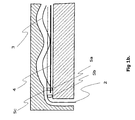
- Figure 1b shows an embodiment of an electromechanical assembly according to the invention to electrically connecting 5 the electromechanical assembly to the main electronic device, energy source or other electronic functionality unit.
- this connecting means 5a, 5b, 5c are arranged from a printed wired foil 4 and/or from a printed foil 2 to the engine printed wired board of the electronic device and/or when necessary between the printed wired foil and the printed foil.
- These connecting means are attached on their other end to the printed wired foil or the printed foil to form the electrical connection.
- figure 1b depicts a detail of figure 1a (area A) it doesn't mean that the connecting means would always be locating within this area A, but said connecting means may be located freely anywhere along the printed (wired) foils in association with the electromechanical assembly.
- the connecting means 5a, 5b, 5c are discussed more detail in connection with figures 4a and 4b .
- the cover part is manufactured by the injection moulding technology which is also called the in mould tecnology or in mould decoration (IMD) technology.
- IMD in mould decoration
- the electromechanical assembly is arranged to be an insert which is integrated into the cover part to compose an integrated combination which is detachable from the electronic device.
- a first mould 12 under the electromechanical assembly and a second mould 11 on top of the electromechanical assembly is needed.
- a cavity 15, 16 where the electromechanical assembly is arranged so that connecting means 5a, 5b are arranged to be located at the electrical contact points 5 between the printed wired foil 3 and the first mould 12 and/or between the printed foil 2 and the first 3 and the first mould 12 and/or between the printed foil 2 and the first mould 12 during the injection moulding.
- a printed foil 2 is arranged on top of the electromechanical assembly and the second mould 11 is set on top of the printed foil 2 so that the lower end of the first mould 12 and the printed foil 2 are engaged to each other, i.e. the cavity 15 above the electromechanical assembly disappears.
- the lower end of the second mould 11 is formed to follow a shape an outer part of the electromechanical assembly.
- a supporting foil 6 is arranged to support the electromechanical assembly from bottom side 4, the support layer also comprising a light source (not shown) to be directed upwards (see figure 2 ).
- a light source not shown
- the resin e.g. engineering plastic
- the resin is injected through the hole 14 of the first mould 12 to the back of the electromechanical assembly to fill with plastics the cavity area 16.
- joints 18 between the printed foil 2 and the printed wired foil 3 will be melted together to form a sealed joint (see figure 3a ).
- the printed foil is a customized injection moulding (CIM) foil 2.
- a front cover 1, so called A-cover, of the portable electronic device, as shown in figure 2 is arranged on top of the electromechanical assembly 3, 4 and the second mould 11 is set on top of the front cover so that the lower end of the second mould and the front cover are engaged to each other, i.e. the cavity 15 above the electromechanical assembly disappears.
- a supporting foil 6 is arranged to support the electromechanical assembly from bottom side 4, the support layer also comprising a light source to be directed upwards, and an additional supporting foil 9 may be installed under a supporting foil 6 if wanted (see figure 3b ).
- a hole 17 through the supporting foils 6, 9 is arranged for electrical contacts to the electronic device so that the connecting means 5a, 5b are piped through the hole 17.
- connecting means 5a, 5b are installed after the injection moulding process.
- the connecting means are any type of small, medium-size or even rather large-size connectors, such as pogo pin connectors and spring connectors are used, and they are assembled afterwards.
- a printed foil 2 is arranged on top of the electromechanical assembly and the second mould 11 is set on top of the printed foil 2 so that the lower end of the first mould 12 and the printed foil 2 are engaged to each other, i.e. the cavity 15 above the electromechanical assembly disappears.
- the lower end of the second mould 11 is formed to follow a shape an outer part of the electromechanical assembly.
- a supporting foil 6 is arranged to support the electromechanical assembly from bottom side 4, the support layer also comprising a light source (not shown) to be directed upwards (see figure 2 ).
- the printed foil is a customized injection moulding (CIM) foil 2.
- a front cover 1, so called A-cover, of the portable electronic device, as shown in figure 2 is arranged on top of the electromechanical assembly 3, 4 and the second mould 11 is set on top of the front cover so that the lower end of the second mould and the front cover are engaged to each other, i.e. the cavity 15 above the electromechanical assembly disappears.
- a supporting foil 6 is arranged to support the electromechanical assembly from bottom side 4, the support layer also comprising a light source to be directed upwards, and an additional supporting foil 9 may be installed under a supporting foil 6 if wanted (see figure 3b ).
- a hole 17 through the supporting foils 6, 9 is arranged for electrical contacts to the electronic device so that the connecting means 5a, 5b are piped through the hole 17.
- connecting means 5a, 5b are installed after the injection moulding process.
- the connecting means are any type of small, medium-size or even rather large-size connectors, such as pogo pin connectors and spring connectors are used, and they are assembled afterwards.
- the printed foil 2 is a customized injection moulding (CIM) foil.
- CIM foil is used to forge the decoration with desired texts, patterns, images, pictures or alike layouts to in-mould decoration (IMD) objects.
- IMD in-mould decoration
- the wiring can be implemented to the foil during the printing process before starting the IMD process.
- the CIM foil as a printed foil 2 is like a printed wired foil 3 in relation to electrical connectivity.
- a CIM foil 2 is arranged on top of the keypad assembly 3, 4 and the second mould 11 is set on top of the CIM foil so that the lower end of the second mould and the CIM foil are engaged to each other, i.e. the cavity 15 above the keypad assembly disappears.
- the lower end of the second mould 11 is formed to follow a shape of domes 3 of the keypad assembly.
- a supporting foil 6 is arranged to support the keypad assembly from bottom side 4, the support layer also comprising a light source to be directed upwards (see figure 2 ).
- the resin e.g. engineering plastic
- joints 18 between the CIM foil 2 and the printed wired foil 3 will be melted together to form a sealed joint (see figure 3a ).
- a front cover 1, so called A-cover, of the portable electronic device is arranged on top of the keypad assembly 3, 4 and the second mould 11 is set on top of the cover so that the lower end of the second mould and the cover are engaged to each other, i.e. the cavity 15 above the keypad assembly disappears.
- the first and second mould are arranged in figure 2 (not depicted) in the same way as in figures 1a and 1c .
- a supporting foil 6 is arranged to support the keypad assembly from bottom side 4, the support layer also comprising a light source to be directed upwards, and an additional supporting foil 9 may be installed under a supporting foil 6 if wanted (see figure 3b ).
- a hole 17 through the foils 6, 9 is arranged for electrical contacts to the electronic device.
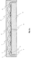
- Figures 3a and 3b show a keypad structure of the keypad assembly according to the invention.
- Figure 3a shows a detail structure of one keydome of the keypad of the keyboard which keyboard is put as an insert into the mould 11, 12 before the injection molding.
- the keypad comprises a printed foil 3 and a printed wired foil 4 wherein decorations and other graphics details are arrenged to a lower surface of the printed foil 3, an upper surface of the printed foil 3 is arrenged to be finger touchable and electrical connections are arrenged to an upper surface of the printed wired foil 4.
- the printed foil is arranged to be above the printed wired foil.
- a dome sheet layer 7 is placed between the printed foil and the printed wired foil, wherein the dome sheet 7 is electrically conductive at least at the concave surface 8 of each dome.
- the printed wired foil 4 comprises wiring for electrically connecting contact points of the concave surface 8 of each dome to each other and to the contact points for connections to the electronic device. According to one embodiment the contact points to the electronic device are connected via the hole 17a through the supporting foil 6 and possible additional supporting foil 9 as shown in figure 3b .
- the keypad comprises two printed wired foils 3, 4, preferably a multi-layer printed wired foil 3, 4 wherein electrical connections are arranged to a lower surface of a first printed wired foil 3 and an upper surface of a second printed wired foil 4.
- An upper surface of the first printed wired foil 3 is arranged to be finger touchable.
- the first printed wired foil is arranged to be above the second printed wired foil.
- a dome sheet layer 7 is placed between the first and second printed wired foil, wherein the dome sheet 7 is electrically conductive at least at the concave surface 8 of each dome.
- the second printed wired foil 4 comprises wiring for electrically connecting contact points of the concave surface 8 of each dome to each other and to the contact points for connections to the electronic device.
- the contact points to the electronic device are connected via the hole 17a through the supporting foil 6 and possible additional supporting foil 9 as shown in figure 3b .
- a supporting foil 6 is arranged to support the keypad assembly from bottom side 4, the support layer also comprising a light source to be directed upwards, and an additional supporting foil 9 may be installed under a supporting foil 6 if needed.
- the light source in association with the supporting foil 6 is arranged by e.g. a rigid light guide or an electroluminescence foil, and the light is arranged to come out only in the place of keys upwards.
- Figures 4a and 4b show examples of electrically connecting an electromechanical assembly according to the invention to the electronic device, power source or other electronic functionality unit.
- connecting means 5 which is attached on its first end to the contact points 21 on the printed wired foil 4.
- the connecting means is preferably a connector 5 which is soldered, glued or other way fixed to a contact pad 21 on a flexible printed wired board or printed wired foil 4 before the injection mould process.
- Any small and universal connectors may be used, preferably a connector in a shape of a metallic cylinder, e.g. R-pin connectors.
- the connector being part of the electromechanical assembly will be covered totally with plastics.
- a second end of the connector 5 which forms so called R-pins, is either a little bit protruding out of the mould 19 or a little bit inside the mould 19.
- the mould 19 is representing a piece of the cover part of the electronic device and a reference number 19a relates to that edge of the cover part where the connectors have outlets from the cover part.
- the second end of the connector 5 is forming a contact pin to be electrically connected to the engine PWB of the electronic device.
- these type of connectors are used to connect the inmold electronics of the electromechanical assembly being inside the cover part to the surface of the mechanical part of the cover part and further to the engine PWB and/or energy source.
- Figure 4b shows connecting means 5a, 5b, 5c for electrically connecting the printed wired foil 4 to the engine PWB or energy source (5a), the printed foil, preferably the CIM foil 2, to the engine PWB (5b) and the printed foil, preferably CIM foil 2, to the printed wired foil 4 (5c).
- the CIM foil as a printed foil, having printed wiring and decoration, is like the printed wired foil in relation to electrical connectivity properties.
- the connecting means is preferably a connector 5a, 5b, 5c which is soldered, glued or other way fixed to a contact pad on a flexible printed wired board or printed wired foil 4 before the injection mould process. Any small and universal connectors may be used, preferably in a shape of metallic cylinder, e.g.
- R-pin connectors When the injection mould process is completed a second end of the connector 5a, 5b, which forms so called R-pins, is either a little bit protruding out of the mould 19 or a little bit inside the mould 19 and then the second end of the connector with R-pins is exposed by mechanical grinding of the plastic surface.
- the connecting means 5c is fixed firmly between the foils 2, 4 and it is any small type of appropriate connector such as R pin connector, spring connector or jumper connection.
- Figure 5 shows a method for manufacturing an electromechanical assembly and a cover part for an electronic device, the electromechanical assembly comprising at least a printed wired foil, and the electronic device comprising at least one cover part.
- the electromechanical assembly and the cover part are manufactured using the same manufacturing technology and process which facilitates and makes cost effective the manufacturing of the electronic device.
- the method comprising steps where in steps 101 - 111 the printed wired foil is electrically connected to the electromechanical assembly and to the electronic device and in step 113 the electromechanical assembly and the cover part is composed to be an integrated combination which is detachable from the electronic device.
- the cover part will be detachably mechanically connected to the electronic device.
- the method comprises a step 113 of integrating the electromechanical assembly into the cover part to compose an integrated combination which is detachable from the electronic device.
- the step 101 - 111 of electrically connecting comprises further steps, where in step 101 the wiring onto the printed wired foil, preferably a multi-layer printed wired foil, is provided by printing with conductive ink electrical connections to contact points and between the contact points for components of the electromechanical assembly, and to contact points electrically connecting the electromechanical assembly to the electronic device, preferably to an engine printed wired board.
- the conductive ink is a silver polymer paste.
- the isolation layers are printed with non-conductive ink onto the printed wired foil, and in step 105 decorations are printed with coloured ink onto the printed wired foil, or alternatively onto the printed foil.
- the step 101 of electrically connecting comprises further step of printing with conductive ink the wiring onto the printed wired foil to provide electrical connections to at least one contact point electrically connecting the electromechanical assembly to a tactile feed back component of the electronic device.
- the electromechanical assembly is electrically connected via the contact point from the electromechanical assembly to the electronic device, preferably to the engine printed wired board, and/or to the power source.
- the connecting means are attached on their other end to the printed wired foil and/or printed foil, preferably the CIM foil, to form the electrical connection to the electronic device, power source or other electronic tion to the electronic device, power source or other electronic functionality unit.
- the other endo of small universal connectors preferably metallic cylindrical R pin connectors, are soldered or glued to the contact point on the printed wired foil and/or CIM foil.
- the step of electrically connecting comprises further a step 107 of cutting a hole through the printed wired foil at the contact point to provide electrical connection to other electronic functionality unit, e.g. the tactile feedback component, to be located on the opposite side of the cover part than other connecting means.
- step 107 is a through hole wiring by laser to provide electrical contacts to outside surface for user interface sensors, such as a fat percentage detector.
- the step 101 - 111 of electrically connecting comprises step 101 of printing a lower surface of a first printed wired foil and processing an upper surface of the first printed wired foil to be finger touchable, and printing an upper surface of a second printed wired foil, the first printed wired foil being above the second printed wired foil, and placing a dome sheet layer between the first and second printed wired foil, wherein the dome sheet is electrically conductive at the concave surface of each dome.
- the step 101 - 111 of electrically connecting comprises step 101 of printing an upper surface of a printed wired foil, and step 105 of printing a lower surface of a printed foil and processing an upper surface of the printed foil to be finger touchable, the printed foil being above the printed wired foil, and placing a dome sheet layer between the printed foil and the printed wired foil, wherein the dome sheet is electrically conductive at the concave surface of each dome.
- step 109 a formed printed wired foil is generated by the thermoforming of the printed wired foil to a desired shape.
- a formed printed wired foil is generated by the thermoforming of the combination of the printed foil and the printed wired foil to a desired shape.
- step 111 follows to mount electrical and mechanical components to the formed printed wired foil.
- the step 111 of mounting mechanical components comprises mounting a keymat to the formed printed wired foil and printing with conductive ink the wiring onto the keymat to provide electrical connections to contact points and between the contact points for keypad of the electromechanical assembly.
- step 111 of mounting comprises placing a support layer under the second printed wired foil, functionality unit.
- the other endo of small universal connectors preferably metallic cylindrical R pin connectors, are soldered or glued to the contact point on the printed wired foil and/or CIM foil.
- the step of electrically connecting comprises further a step 107 of cutting a hole through the printed wired foil at the contact point to provide electrical connection to other electronic functionality unit, e.g. the tactile feedback component, to be located on the opposite side of the cover part than other connecting means.
- step 107 is a through hole wiring by laser to provide electrical contacts to outside surface for user interface sensors, such as a fat percentage detector.
- the step 101 - 111 of electrically connecting comprises step 101 of printing a lower surface of a first printed wired foil and processing an upper surface of the first printed wired foil to be finger touchable, and printing an upper surface of a second printed wired foil, the first printed wired foil being above the second printed wired foil, and placing a dome sheet layer between the first and second printed wired foil, wherein the dome sheet is electrically conductive at the concave surface of each dome.
- the step 101 - 111 of electrically connecting comprises step 101 of printing an upper surface of a printed wired foil, and step 105 of printing a lower, surface of a printed foil and processing an upper surface of the printed foil to be finger touchable, the printed foil being above the printed wired foil, and placing a dome sheet layer between the printed foil and the printed wired foil, wherein the dome sheet is electrically conductive at the concave surface of each dome.
- step 109 a formed printed wired foil is generated by the thermoforming of the printed wired foil to a desired shape.
- a formed printed wired foil is generated by the thermoforming of the combination of the printed foil and the printed wired foil to a desired shape.
- step 111 follows to mount electrical and mechanical components to the formed printed wired foil.
- the step 111 of mounting mechanical components comprises mounting a keymat to the formed printed wired foil and printing with conductive ink the wiring onto the keymat to provide electrical connections to contact points and between the contact points for keypad of the electromechanical assembly.
- step 111 of mounting comprises placing a support layer under the second printed wired foil, which support layer comprises a light source, e.g.
- step 111 of mounting comprises placing a support layer under the combination of the printed foil and the printed wired foil.
- step 111 is mounting of separated components like leds, resistors to the formed printed wired foil using anisotropically conductive glue or conductive tapes.
- step 111 is an electromechanical assembly, which will be as an insert to be put into mould before the injection mould process.
- the electromechanical assembly and the cover part is composed to be an integrated combination, preferably the electromechanical assembly is integrated into the cover part to compose an integrated combination, which will be detachable from the electronic device.
- the electromechanical assembly is a formed printed wired foil which an insert during the injection moulding process.
- the electromechanical assembly is an insert during the injection moulding process.
- the formed printed wired foil, or alternatively the formed combination of the printed foil and the printed wired foil is placed as an insert to the mould and the molten resin, e.g. molten plastics, is injected e.g. by a nozzle head to the mould to form tactile taps and a terminal cover.
- the formed printed wired foil is inserted on top of a mould comprising a through hole, preferably a vertical hole, and the connecting means of the formed printed wired foil are directed to a position towards the mould (see figure 1a ).
- a printed foil referred here as a cover foil
- Another mould is then placed on top of the cover foil so that a cavity is provided between the lower mould and the formed printed wired foil, and a lower edge of the upper mould is engaged to follow a shape of the formed printed wired foil.
- the moulds are arranged to hold still, and finally, molten resin e.g. plastic is injected via the through hole to the cavity between the upper and lower moulds.
- the formed printed wired foil is inserted on top of a mould comprising a through hole, preferably a vertical hole, and a bump on top and the formed printed wired foil is placed to a position where the bump masks the contact points from the electromechanical assembly to the electronic device (see figure 1c ). Then a cover foil is placed on top of the formed printed wired foil. Another mould is then placed on top of the cover foil so that a cavity is provided between the lower mould and the formed printed wired foil, and a lower edge of the upper mould is engaged to follow a shape of the formed printed wired foil. Then the moulds are arranged to hold still, and finally, molten resin e.g. plastic is injected via the through hole to the cavity between the upper and lower moulds.
- molten resin e.g. plastic is injected via the through hole to the cavity between the upper and lower moulds.
- a cover foil is placed on top of the formed printed wired foil, preferably a perforated cover foil is placed on top of the formed printed wired foil comprising a dome sheet layer, wherein a perforation of the cover foil is locating at the location of the dome of the dome sheet, so that the perforated cover foil and the formed printed wired foil with domes compose a solid combination.
- a cover foil is a CIM foil, preferably a perforated CIM foil.
- molten resin e.g. molten plastic is injected to seam joints between edges of the perforations of the cover foil, preferably CIM foil, and the dome sheet during the injection moulding.
- step 115 the combination of the cover part and the electromechanical assembly is electrically connected by connecting means to the electronic device, preferably to the engine printed wired board, power source or other electronic functionality unit.
- Step 115 comprises a preliminary step of cleaning the outlets of the connecting means by grinding the surface of the plastic cover to expose the contact pins of the contactor, preferably R pin contactor, after the injection mould process. This can be done by a mechanical grinder.
- the combination of the cover part and the electromechanical assembly is electrically connected via the contact point from the electromechanical assembly to the electronic device, preferably to the engine printed wired board, power source or other electronic functionality unit.
- the cover part electronics is connected to the main portable device with a connector having spicular or pin coupling, e.g. pogo pins or spring connectors.
- the manufacturing technology according to the invention allow for complete sealing of the components into a plastic resin which is beneficial for wear, shock and moisture protection. Also the manufacturing technology with in moulded covers and overmoulded components provides an excellent prerequisite for making the user interface watertight. It also provides a prerequisite for extreme miniaturisation because the technology takes to active use the volume that has been used for pure mechanics.
- the manufacturing technology according to the invention also provides a cheap way for producing portable products.
- the printing of conductors, e.g. screen printing, into the foil is highly cost effective because it is integrated into the graphics printing of the cover part of the portable device.
- the technology in addition removes a need for many components, such as key buttons from keypads, and provides room for new functionality on the engine PWB.
Landscapes
- Engineering & Computer Science (AREA)
- Theoretical Computer Science (AREA)
- General Engineering & Computer Science (AREA)
- Manufacturing & Machinery (AREA)
- General Physics & Mathematics (AREA)
- Physics & Mathematics (AREA)
- Human Computer Interaction (AREA)
- Mechanical Engineering (AREA)
- Microelectronics & Electronic Packaging (AREA)
- Casings For Electric Apparatus (AREA)
- Switch Cases, Indication, And Locking (AREA)
- Telephone Set Structure (AREA)
- Push-Button Switches (AREA)
Abstract
Description
- The present invention relates generally to the electromechanical structures of portable electronic devices, electronic circuits, printed wired boards, electronic components and encapsulation. Especially the invention concerns the integration of electromechanical keypad arrangements and mechanical parts of an electronic device.
- An input device is an important part of many portable electronic devices and it is used to control operation and input information to the electronic device. In portable electronic devices such as computers, communication devices, measuring devices and similar devices the most common input devices used are keypads, keyboards and touch panels consisting of individually pressable or touchable numeric or alphanumeric, function and control keys. To activate these kind of input devices a user must press or touch a certain key or a certain touch point to accomplish a desired operation.
- A known structural arrangement is to build up a keypad system on a printed wired board (PWB) with a number of contact pads on its upper surface. In this description the printed wired board (PWB) is used as an general designation for both the PCB and the PWB. The actual key switches are located on the PWB at the points where conductive input rows and conductive output columns form a junction, i.e. a key switch, comprising a conductive dome. An insulating film covers the PWB except of those contact pads onto which components are to be placed. The keypad part comprises a dome sheet or alternatively a selection of individual key domes made of some resilient material that is electrically conductive at least at the concave surface of each dome. Additionally the keypad part comprises a rubbery keymat where the bulging protrusions coincide with the conductive domes of the dome sheet and constitute the visible parts of the keys. Pressing the key will cause the conductive dome to produce an electrical contact at the key switch.
- In portable electronic devices such as mobile phones, communicators and laptops the keypad arrangement is built on the "engine PWB". The engine PWB is a common designator of such printed wired boards that comprise a remarkable number of electronic components that implement the main functionalities of the telecommunication device. The electronic part of the portable device, the engine PWB being part of this electronic module, is usually encapsulated so that it is of this electronic module, is usually encapsulated so that it is shielded against electromagnetic interference and other disturbancies. Thus the electronic part constitutes its own entity which is then enclosed in the outer casing forming the cover part of the portable device. The rubbery keymat with bulging protrusions constitutes one side of the electronic part of the portable device and this side will abut on the cover part with openings fixed for bulging protrusions. The electronic part and cover part is then anchored to each other with fasteners.
- In document
WO 01/48771 - Today manufacturing processes for keypad arrangements and cover parts of portable devices are totally different and are commonly performed even in separate manufacturing facilities by different providers or sub-contractors. The keypad arrangement including circuitry, electronic components and sheet material components is manufactured by conventional PWB manufacturing processes including screen printing, component assembling and reflow soldering. The cover part is generally manufactured by engineering plastic moulding processes.
- A printed wired board (PWB) or a printed wiring board is a rigid support with connections in the form of flat metal strips. Typically the connections are "printed" as a pattern of lines of etch-resist ink over a uniform metal coating on the board. Etching removes the unmasked regions, leaving the interconnect lines. The etch-resist is then also washed off, leaving the wires exposed and available for connection. At the ends of the lines, holes may be drilled to allow the leads of surface components or sockets to be passed through. Discrete components like resistors and power transistors are inserted directly. Microchips an alike are soldered on directly or sockets are soldered onto the board where these active components are then inserted.
- Exchangeable covers have gained popularity especially among young consumers who want visually-differentiated cover parts to their portable electronic devices. The cover part can be decorated using so called in mould decoration (IMD) processes which are gaining ground nowadays. This technique consists of the decoration of an injection moulded part during the moulding process. A special carrier film or foil, which is also called in mould decoration (IMD) foil or customized injection mould (CIM) foil, is used to forge the decoration to the cover part. In the IMD process a flat piece of film or foil is first decorated with desired texts, patterns, images, pictures or alike layouts and then the film is formed to fit the profile of the injection mould and cut to shape. After that the film is inserted as an insert into a mould cavity, where finally moulding resin is injected onto the back of the film. The resin fuses onto the back of the film, and the materials are bonded together. The cover part is now complete and no post-processing is required. As high temperature moulding resins typically polycarbonate, ABS and blends are used. ABS is an acronym for acrylonitrile-butadiene-styrene copolymers, which are elastomer-modified styrene plastics (thermoplastic). For example, key caps and buttons made of preprinted foil can be implemented in the cover parts formed from in-coloured coextruded film using IMD process.
- Today, high pressure formed decorative printed foil keypads with back injection moulded taps using IMD technology are widely used in electronics and this same technology is also used in cover part manufacturing. These keypads and covers need a separate printed wired board for user interface connections, tactile feed back and other electronic functionality, which separate PWB is physically locating in connection with the electronic part of the portable device.
- The need for miniaturization of portable electronic devices sets limits to the size of the electronic part comprising the engine PWB which is a reason why the engine PWB is used as an electronic platform for keypad arrangements. This means that the keypad arrangement and the engine PWB layout is fixed to each other and it will be difficult to change the keypad layout without changing the engine PWB. This kind of keypad arrangement limits a lot the freedom to design differentiated keypad layouts to exchangeable cover parts of the portable electronic devices.
- In view of various inherent limitations of integrating keypad arrangements flexibly to the portable electronic devices, it would be desirable to avoid or mitigate these and other problems associated with prior art arrangements. Thus, there is a need for new techniques to provide electronics-mechanics integration for electronic devices.
- It is an object of the invention to provide a electromechanical structure comprising a user interface and a printed wired board, which structure is advantages in terms of manufacturing and offers freedom to the layout design of the printed wired board, the user interface as well as the appearance of the device itself. It is also an object of the invention to provide a electromechanical structure that is compact and facilitates the customizability and upgradability with a new electronic functionality without any need for modifications to the main electronics of the device.
- The objects of the invention are achieved by integrating the electromechanical assembly with the mechanical cover part of the electronic device by using injection moulding process to compose an integrated combination which is detachable from the electronic device. More precisely the objects of the invention are achieved by combining the injection moulding technologies with the printing of electronic wired boards.
- In accordance with a first aspect of the invention there is provided an electromechanical assembly for an electronic device, the electromechanical assembly comprising at least a printed wired foil and means for electrically connecting the electromechanical assembly to the electronic device, the electronic device comprising at least one cover part and means for mechanically connecting the cover part to the electronic device, wherein the electromechanical assembly and the cover part is arranged to compose an integrated combination which is detachable from the electronic device.
- In a preferred embodiment a keypad assembly is provided for integrating the keypad assembly with the cover part to compose an integrated combination which is detachable from the electronic device.
- Preferably, the keypad assembly is integrated into the cover part.
- In another preferred embodiment a touch sensor assembly is provided for integrating the the touch sensor assembly with the cover part to compose an integrated combination which is detachable from the electronic device.
- Preferably, the touch sensor assembly is integrated into the cover part.
- In accordance with a third aspect of the invention there is provided a method for manufacturing an electromechanical assembly for an electronic device, the electromechanical assembly comprising at least a printed wired foil, and the electronic device comprising at least one cover part, the method comprising steps:
- electrically connecting the printed wired foil to the electromechanical assembly and to the electronic device,
- mechanically connecting the cover part to the electronic device, and
- composing the electromechanical assembly and the cover part to be an integrated combination which is detachable from the electronic device.
- In a preferred embodiment a method for manufacturing a keypad assembly is provided for integrating the keypad assembly with the cover part to compose an integrated combination which is detachable from the electronic device.
- Preferably, the keypad assembly is integrated into the cover part.
- In another preferred embodiment a method for manufacturing a touch sensor assembly is provided for integrating the touch sensor assembly with the cover part to compose an integrated combination which is detachable from the electronic device.
- Preferably, the touch sensor assembly is integrated into the cover part.
- According to the invention all electronic components including connectors outwards, electronic printed wired boards associated with the user interface and other input/output devices as well as mechanical components are structurally associated with a cover part and not with an "engine PWB" which is a common designator of such printed wired boards that comprise a remarkable number of electronic components that implement the main functionalities of an electronic device.
- As a consequence of the invention numerous advantages are achieved. The layout design of the user interface and the printed wired board is freed from the characteristics and design of the main electronic device and the standardized engine PWB layout. In portable electronics there is a drive to standardize the engine PWB, but at the same time there is a drive to expand the types of user interfaces of the portable devices. A great degree of freedom is given to design of cover parts and exchangeable outer covers. The manufacturing technologies and processes according to the invention also allow new electronic functions to be produced in the cover part. The location, number and size of electronic functional elements become completely independent of the engine PWB layout. Minituarisation is made possible because large areas of the engine PWB surface space are left free, or the saved PWB surface is free for other use. Realization of watertight and hermetically sealed touch-controlled electronic devices become easier to produce because the manufacturing technology enables complete sealing of the electromechanical assembly and user interface when enfold into the plastic resin. The manufacturing process according to invention is affordable in price.
- The novel features which are considered as characteristic of the invention are set forth in particular in the appended claims. The invention itself, however, both as to its construction and its method of operation, together with additional objects and advantages thereof, will be best understood from the following description of specific embodiments when read in connection with the accompanying drawings.
-
Figure 1a shows a cross-section diagram of an embodiment of an electromechanical assembly according to of the invention and an arrangement for manufacture a cover part comprising the electromechanical assembly as an insert during injection moulding. -
Figure 1b shows more detailed the area A offigure 1 . -
Figure 1c shows a cross-section diagram of one embodiment of an electromechanical assembly according to the invention. -
Figure 2 shows a cross-section diagram of another embodiment of an electromechanical assembly according to the invention. -
Figure 3a shows a cross-section diagram of a keypad structure according one embodiment of the electromechanical assembly. -
Figure 3b shows a cross-section diagram of a keypad structure according another embodiment of the electromechanical assembly. -
Figure 4a shows one embodiment of the invention to electrically connecting an electromechanical assembly and a cover part to the main electronic device. -
Figure 4b shows other embodiments of the invention to electrically connecting an electromechanical assembly and a cover part to the main electronic device. -
Figure 5 shows a block diagram of an embodiment of a method for manufacturing an electromechanical assembly and a cover part combined together according to the invention. - An electromechanical assembly for an electronic device comprises both electrical and mechanical function components which will be part of the electronic device. Typically an electromechanical assembly is an input/output device to relay information from user to the electronic unit of the electronic device, and vice versa. The input/output device is activated by pressing, touching, blowing or acting other physical manner to the user interface of the input/output device. In this description the term assembly is used to describe that the system comprises both electronic and mechanical components, e.g. a keypad assembly comprises electronic components such as conductors, resistors, detectors, leds etc. on a printed wired board and mechanical components such as keydomes on a printed wired board. In portable electronic devices multi-layer foils made of flexible conductive material are commonly used as a platform for an electronic circuitry instead of printed wired boards. Thus, in this description the term printed wired foil is used instead of printed wired board.
- In portable electronic devices such as mobile phones there is a drive to standardize the engine PWB, but at the same time there is a drive to expand the types of user interfaces such as keypads of the portable devices. In case of the keypad where the actual key switches, domes and pads are usually on the engine printed wired board (PWB) this causes a problem because the keypad layout cannot be changed without changing the engine PWB layout. To overcome this problem is accomplished by separating the keypad from the engine PWB and placing it into the front or back cover of the mobile phone. By doing so the keypad is not part of the engine hardware of the mobile phone and any layouts of user interfaces can be produced, and a customer can choose the one or the ones he wants to have, just buying an add on cover. It is also possible to integrate special user interfaces into the cover parts of the mobile phone to be used for e.g. gaming, picture editing and chinese handwriting recognition. The manufacturing technologies and processes according to the invention also enable new functions to be produced in the phone cover which means that a customer can select and buy new functionalities for his mobile phone at any time, not just when he initially purchases the mobile phone.
- The invention presented covers mainly three different domains, namely firstly an idea of printing conductors and electronics onto an in mould decoration (IMD) foil prior to its forming, secondly a manufacturing process that is utilized, and thirdly technological components, such as conductive ink and interconnects to the printed electronics, that are needed.
-
Figure 1a shows an electromechanical assembly comprising a printedwired foil figures 1b ,4a and 4b ). The printedwired foil points 5 electrically connecting the electromechanical assembly to the electronic device, isolation layers and decorations, and electronic and mechanical components mounted on the appropriate contact points onto the printed wired foil. Preferably, the printed wired foil comprises wiring to providecontact points 5 electrically connecting the electromechanical assembly to the engine printed wired board. - According to a first embodiment of the invention an electromechanical assembly is an
input decive assembly input device 3 connected to a printedwired foil 4 and means for electrically connecting 5 the input device assembly to the electronic device. According to a second embodiment of the invention the electromechanical assembly is akeypad assembly keypad arrangement 3 connected to a printedwired foil 4 and means for electrically connecting 5 the keypad assembly to the electronic device (see more detailed description in association tofigures 3a and 3b ). According to a third embodiment of the invention the electromechanical assembly is atouch sensor assembly touch sensor arrangement 3 connected to a printedwired foil 4 and means for electrically connecting 5 the touch sensor assembly to the electronic device. Preferably, the printed wired foil comprises wiring to provide contact points electrically connecting the electromechanical assembly to a tactile feed back component of the electronic device. According to a fourth embodiment of the invention the electromechanical assembly is anyuser interface assembly user interface device 3 connected to a printedwired foil 4 and means for electrically connecting 5 the user interface assembly to the electronic device. According to a fifth embodiment of the invention the electromechanical assembly is afunctional device assembly functional device 3 connected to a printedwired foil 4 and means for electrically connecting 5 the functional device assembly to the electronic device. - Some applications of the electromechanical assembly according to the embodiments of the invention listed above are for example different modules with control electronics: all types of keypads and keyboards, touch-controlled sensors such as a handwriting recognation detector, a picture editing detector and a fat percentage detector, different types of user interface modules, and different types of funtionality modules such as a location detector, a flashlight circuit and a camera circuit.
- Some examples of electronic devices into which the functionality of above mentioned electromechanical assemblies can be integrated are the following portable electronic devices: a mobile phone, a communicator, a portable digital assistant (PDA), a palmtop computer, a laptop computer, a web terminal equipment, a digital camera, a game computer and an entertainment device, and as well portable measuring and testing devices. The requirements for portable electronic devices are compactness, small size, lightness, robustness and reliability. Among users of portable electronics there is a gaining aspiration to personalize the user interface and outlook of the device, which means that customizability and upgradability are also requirements of the modem portable device. More and more, there is a need for several user interfaces for different purposes to be used in a single portable electronic device as a platform. A solution for this is the use of exchangeable user interfaces in the same way as exchangeable cover parts, which are decorated in various ways, are used today in portable electronics, such as mobile phones.
- The electronic device comprising a cover part and means for mechanically connecting the cover part to the electronic device is arranged. According to the invention the
electromechanical assembly electromechanical assembly input device assembly keypad assembly touch sensor assembly -
Figure 1b shows an embodiment of an electromechanical assembly according to the invention to electrically connecting 5 the electromechanical assembly to the main electronic device, energy source or other electronic functionality unit. To do this connecting means 5a, 5b, 5c are arranged from a printedwired foil 4 and/or from a printedfoil 2 to the engine printed wired board of the electronic device and/or when necessary between the printed wired foil and the printed foil. These connecting means are attached on their other end to the printed wired foil or the printed foil to form the electrical connection. Whilefigure 1b depicts a detail offigure 1a (area A) it doesn't mean that the connecting means would always be locating within this area A, but said connecting means may be located freely anywhere along the printed (wired) foils in association with the electromechanical assembly. The connecting means 5a, 5b, 5c are discussed more detail in connection withfigures 4a and 4b . - The cover part is manufactured by the injection moulding technology which is also called the in mould tecnology or in mould decoration (IMD) technology. During the IMD process the electromechanical assembly is arranged to be an insert which is integrated into the cover part to compose an integrated combination which is detachable from the electronic device. To do this, as shown in
figure 1a , afirst mould 12 under the electromechanical assembly and asecond mould 11 on top of the electromechanical assembly is needed. Between the moulds is fixed acavity electrical contact points 5 between the printedwired foil 3 and thefirst mould 12 and/or between the printedfoil 2 and the first 3 and thefirst mould 12 and/or between the printedfoil 2 and thefirst mould 12 during the injection moulding. According an embodiment of the invention a printedfoil 2 is arranged on top of the electromechanical assembly and thesecond mould 11 is set on top of the printedfoil 2 so that the lower end of thefirst mould 12 and the printedfoil 2 are engaged to each other, i.e. thecavity 15 above the electromechanical assembly disappears. The lower end of thesecond mould 11 is formed to follow a shape an outer part of the electromechanical assembly. A supportingfoil 6 is arranged to support the electromechanical assembly frombottom side 4, the support layer also comprising a light source (not shown) to be directed upwards (seefigure 2 ). When the resin, e.g. engineering plastic, is injected through thehole 14 of thefirst mould 12 to the back of the electromechanical assembly to fill with plastics thecavity area 16. During the injection moulding process joints 18 between the printedfoil 2 and the printedwired foil 3 will be melted together to form a sealed joint (seefigure 3a ). According another embodiment of the invention the printed foil is a customized injection moulding (CIM)foil 2. According still another embodiment of the invention afront cover 1, so called A-cover, of the portable electronic device, as shown infigure 2 , is arranged on top of theelectromechanical assembly second mould 11 is set on top of the front cover so that the lower end of the second mould and the front cover are engaged to each other, i.e. thecavity 15 above the electromechanical assembly disappears. A supportingfoil 6 is arranged to support the electromechanical assembly frombottom side 4, the support layer also comprising a light source to be directed upwards, and an additional supportingfoil 9 may be installed under a supportingfoil 6 if wanted (seefigure 3b ). Ahole 17 through the supportingfoils means hole 17. When the resin, e.g. engineering plastic, is injected through thehole 14 of thefirst mould 12 to the back of the electromechanical assembly to fill with plastics thecavity area 16. - As shown in
figure 1c , according still another embodiment between themoulds cavity bump 13 is arranged to protect theelectrical contact points 5 not to be filled with plastic and leave the contact points unexposed during the injection moulding. According to thisembodiment connecting means -
mould 12 during the injection moulding. According an embodiment of the invention a printedfoil 2 is arranged on top of the electromechanical assembly and thesecond mould 11 is set on top of the printedfoil 2 so that the lower end of thefirst mould 12 and the printedfoil 2 are engaged to each other, i.e. thecavity 15 above the electromechanical assembly disappears. The lower end of thesecond mould 11 is formed to follow a shape an outer part of the electromechanical assembly. A supportingfoil 6 is arranged to support the electromechanical assembly frombottom side 4, the support layer also comprising a light source (not shown) to be directed upwards (seefigure 2 ). When the resin, e.g. engineering plastic, is injected through thehole 14 of thefirst mould 12 to the back of the electromechanical assembly, to feel with plastics thecavity area 16. During the injection moulding process joints 18 between the printedfoil 2 and the printedwired foil 3 will be melted together to form a sealed joint (seefigure 3a ). According another embodiment of the invention the printed foil is a customized injection moulding (CIM)foil 2. According still another embodiment of the invention afront cover 1, so called A-cover, of the portable electronic device, as shown infigure 2 , is arranged on top of theelectromechanical assembly second mould 11 is set on top of the front cover so that the lower end of the second mould and the front cover are engaged to each other, i.e. thecavity 15 above the electromechanical assembly disappears. A supportingfoil 6 is arranged to support the electromechanical assembly frombottom side 4, the support layer also comprising a light source to be directed upwards, and an additional supportingfoil 9 may be installed under a supportingfoil 6 if wanted (seefigure 3b ). Ahole 17 through the supportingfoils means hole 17. When the resin, e.g. engineering plastic, is injected through thehole 14 of thefirst mould 12 to the back of the electromechanical assembly to fill with plastics thecavity area 16. - As shown in
figure 1c , according still another embodiment between themoulds cavity bump 13 is arranged to protect theelectrical contact points 5 not to be filled with plastic and leave the contact points unexposed during the injection moulding. According to thisembodiment connecting means - As mentioned above according to an embodiment of the invention the printed
foil 2 is a customized injection moulding (CIM) foil. It is known that the CIM foil is used to forge the decoration with desired texts, patterns, images, pictures or alike layouts to in-mould decoration (IMD) objects. According to the invention in addition to said decoration also the wiring can be implemented to the foil during the printing process before starting the IMD process. This means that the CIM foil as a printedfoil 2 is like a printedwired foil 3 in relation to electrical connectivity. - According one embodiment of the invention a
CIM foil 2 is arranged on top of thekeypad assembly second mould 11 is set on top of the CIM foil so that the lower end of the second mould and the CIM foil are engaged to each other, i.e. thecavity 15 above the keypad assembly disappears. The lower end of thesecond mould 11 is formed to follow a shape ofdomes 3 of the keypad assembly. A supportingfoil 6 is arranged to support the keypad assembly frombottom side 4, the support layer also comprising a light source to be directed upwards (seefigure 2 ). When the resin, e.g. engineering plastic, is injected through thehole 14 of thefirst mould 12 to the back of the keypad assembly to fill with plastics thecavity area 16. During the injection moulding process joints 18 between theCIM foil 2 and the printedwired foil 3 will be melted together to form a sealed joint (seefigure 3a ). - As shown in
figure 2 , according to another embodiment of the invention afront cover 1, so called A-cover, of the portable electronic device, , is arranged on top of thekeypad assembly second mould 11 is set on top of the cover so that the lower end of the second mould and the cover are engaged to each other, i.e. thecavity 15 above the keypad assembly disappears. The first and second mould are arranged infigure 2 (not depicted) in the same way as infigures 1a and1c . A supportingfoil 6 is arranged to support the keypad assembly frombottom side 4, the support layer also comprising a light source to be directed upwards, and an additional supportingfoil 9 may be installed under a supportingfoil 6 if wanted (seefigure 3b ). Ahole 17 through thefoils hole 14 of thefirst mould 12 to the back of the keypad assembly to fill with plastics thecavity area 16. -
Figures 3a and 3b show a keypad structure of the keypad assembly according to the invention.Figure 3a shows a detail structure of one keydome of the keypad of the keyboard which keyboard is put as an insert into themould foil 3 and a printedwired foil 4 wherein decorations and other graphics details are arrenged to a lower surface of the printedfoil 3, an upper surface of the printedfoil 3 is arrenged to be finger touchable and electrical connections are arrenged to an upper surface of the printedwired foil 4. The printed foil is arranged to be above the printed wired foil. Adome sheet layer 7 is placed between the printed foil and the printed wired foil, wherein thedome sheet 7 is electrically conductive at least at theconcave surface 8 of each dome. The printedwired foil 4 comprises wiring for electrically connecting contact points of theconcave surface 8 of each dome to each other and to the contact points for connections to the electronic device. According to one embodiment the contact points to the electronic device are connected via thehole 17a through the supportingfoil 6 and possible additional supportingfoil 9 as shown infigure 3b . - According to an embodiment of the invention the keypad comprises two printed
wired foils wired foil wired foil 3 and an upper surface of a second printedwired foil 4. An upper surface of the first printedwired foil 3 is arranged to be finger touchable. The first printed wired foil is arranged to be above the second printed wired foil. Adome sheet layer 7 is placed between the first and second printed wired foil, wherein thedome sheet 7 is electrically conductive at least at theconcave surface 8 of each dome. The second printedwired foil 4 comprises wiring for electrically connecting contact points of theconcave surface 8 of each dome to each other and to the contact points for connections to the electronic device. According to one embodiment the contact points to the electronic device are connected via thehole 17a through the supportingfoil 6 and possible additional supportingfoil 9 as shown infigure 3b . - In
figure 3a thejoints 18 between thecover foil 2, which is perfarated with holes in the place of keydomes, and the printedfoil 3, or alternatively the printedwired foil 3, will be melted together to form a sealed joint during the injection moulding. According to one embodiment thejoints 18 between theCIM foil 2, which is perfarated with holes in the place of keydomes, and the printedwired foil 3 will be melted together to form a sealed joint during the injection moulding. According another embodiment of the invention afront cover 1, of the portable electronic device, as shown infigure 3b , is placed on top of thekeypad assembly foil 6 is arranged to support the keypad assembly frombottom side 4, the support layer also comprising a light source to be directed upwards, and an additional supportingfoil 9 may be installed under a supportingfoil 6 if needed. The light source in association with the supportingfoil 6 is arranged by e.g. a rigid light guide or an electroluminescence foil, and the light is arranged to come out only in the place of keys upwards. -
Figures 4a and 4b show examples of electrically connecting an electromechanical assembly according to the invention to the electronic device, power source or other electronic functionality unit. Infigure 4a there is arranged connectingmeans 5 which is attached on its first end to the contact points 21 on the printedwired foil 4. The connecting means is preferably aconnector 5 which is soldered, glued or other way fixed to acontact pad 21 on a flexible printed wired board or printedwired foil 4 before the injection mould process. Any small and universal connectors may be used, preferably a connector in a shape of a metallic cylinder, e.g. R-pin connectors. During the injection mould process the connector being part of the electromechanical assembly will be covered totally with plastics. When the injection mould process is completed a second end of theconnector 5, which forms so called R-pins, is either a little bit protruding out of themould 19 or a little bit inside themould 19. After this the second end of the connector with R-pins is exposed by mechanical grinding of the plastic surface. Infigure 4a themould 19 is representing a piece of the cover part of the electronic device and a reference number 19a relates to that edge of the cover part where the connectors have outlets from the cover part. The second end of theconnector 5 is forming a contact pin to be electrically connected to the engine PWB of the electronic device. In other words, these type of connectors are used to connect the inmold electronics of the electromechanical assembly being inside the cover part to the surface of the mechanical part of the cover part and further to the engine PWB and/or energy source. -
Figure 4b shows connectingmeans wired foil 4 to the engine PWB or energy source (5a), the printed foil, preferably theCIM foil 2, to the engine PWB (5b) and the printed foil, preferablyCIM foil 2, to the printed wired foil 4 (5c). Preferably the CIM foil as a printed foil, having printed wiring and decoration, is like the printed wired foil in relation to electrical connectivity properties. The connecting means is preferably aconnector wired foil 4 before the injection mould process. Any small and universal connectors may be used, preferably in a shape of metallic cylinder, e.g. R-pin connectors. When the injection mould process is completed a second end of theconnector mould 19 or a little bit inside themould 19 and then the second end of the connector with R-pins is exposed by mechanical grinding of the plastic surface. The connecting means 5c is fixed firmly between thefoils -
Figure 5 shows a method for manufacturing an electromechanical assembly and a cover part for an electronic device, the electromechanical assembly comprising at least a printed wired foil, and the electronic device comprising at least one cover part. According to the invention the electromechanical assembly and the cover part are manufactured using the same manufacturing technology and process which facilitates and makes cost effective the manufacturing of the electronic device. The method comprising steps where in steps 101 - 111 the printed wired foil is electrically connected to the electromechanical assembly and to the electronic device and instep 113 the electromechanical assembly and the cover part is composed to be an integrated combination which is detachable from the electronic device. Finally, the cover part will be detachably mechanically connected to the electronic device. According to a preferred embodiment the method comprises astep 113 of integrating the electromechanical assembly into the cover part to compose an integrated combination which is detachable from the electronic device. - According to an embodiment of the invention the step 101 - 111 of electrically connecting comprises further steps, where in
step 101 the wiring onto the printed wired foil, preferably a multi-layer printed wired foil, is provided by printing with conductive ink electrical connections to contact points and between the contact points for components of the electromechanical assembly, and to contact points electrically connecting the electromechanical assembly to the electronic device, preferably to an engine printed wired board. As an example of the conductive ink is a silver polymer paste. Innext step 103 the isolation layers are printed with non-conductive ink onto the printed wired foil, and instep 105 decorations are printed with coloured ink onto the printed wired foil, or alternatively onto the printed foil. According to one embodiment of the invention thestep 101 of electrically connecting comprises further step of printing with conductive ink the wiring onto the printed wired foil to provide electrical connections to at least one contact point electrically connecting the electromechanical assembly to a tactile feed back component of the electronic device. According to another embodiment instep 107 the electromechanical assembly is electrically connected via the contact point from the electromechanical assembly to the electronic device, preferably to the engine printed wired board, and/or to the power source. The connecting means are attached on their other end to the printed wired foil and/or printed foil, preferably the CIM foil, to form the electrical connection to the electronic device, power source or other electronic tion to the electronic device, power source or other electronic functionality unit. As an example, the other endo of small universal connectors, preferably metallic cylindrical R pin connectors, are soldered or glued to the contact point on the printed wired foil and/or CIM foil. - According to still another embodiment the step of electrically connecting comprises further a
step 107 of cutting a hole through the printed wired foil at the contact point to provide electrical connection to other electronic functionality unit, e.g. the tactile feedback component, to be located on the opposite side of the cover part than other connecting means. As an example ofstep 107 is a through hole wiring by laser to provide electrical contacts to outside surface for user interface sensors, such as a fat percentage detector. - According to one embodiment of the invention the step 101 - 111 of electrically connecting comprises
step 101 of printing a lower surface of a first printed wired foil and processing an upper surface of the first printed wired foil to be finger touchable, and printing an upper surface of a second printed wired foil, the first printed wired foil being above the second printed wired foil, and placing a dome sheet layer between the first and second printed wired foil, wherein the dome sheet is electrically conductive at the concave surface of each dome. According to another embodiment of the invention the step 101 - 111 of electrically connecting comprisesstep 101 of printing an upper surface of a printed wired foil, and step 105 of printing a lower surface of a printed foil and processing an upper surface of the printed foil to be finger touchable, the printed foil being above the printed wired foil, and placing a dome sheet layer between the printed foil and the printed wired foil, wherein the dome sheet is electrically conductive at the concave surface of each dome. - Next in step 109 a formed printed wired foil is generated by the thermoforming of the printed wired foil to a desired shape. According to an embodiment of the invention in step 109 a formed printed wired foil is generated by the thermoforming of the combination of the printed foil and the printed wired foil to a desired shape. Then step 111 follows to mount electrical and mechanical components to the formed printed wired foil. According to one embodiment the
step 111 of mounting mechanical components comprises mounting a keymat to the formed printed wired foil and printing with conductive ink the wiring onto the keymat to provide electrical connections to contact points and between the contact points for keypad of the electromechanical assembly. According to another embodiment thestep 111 of mounting comprises placing a support layer under the second printed wired foil, functionality unit. As an example, the other endo of small universal connectors, preferably metallic cylindrical R pin connectors, are soldered or glued to the contact point on the printed wired foil and/or CIM foil. - According to still another embodiment the step of electrically connecting comprises further a
step 107 of cutting a hole through the printed wired foil at the contact point to provide electrical connection to other electronic functionality unit, e.g. the tactile feedback component, to be located on the opposite side of the cover part than other connecting means. As an example ofstep 107 is a through hole wiring by laser to provide electrical contacts to outside surface for user interface sensors, such as a fat percentage detector. - According to one embodiment of the invention the step 101 - 111 of electrically connecting comprises
step 101 of printing a lower surface of a first printed wired foil and processing an upper surface of the first printed wired foil to be finger touchable, and printing an upper surface of a second printed wired foil, the first printed wired foil being above the second printed wired foil, and placing a dome sheet layer between the first and second printed wired foil, wherein the dome sheet is electrically conductive at the concave surface of each dome. According to another embodiment of the invention the step 101 - 111 of electrically connecting comprisesstep 101 of printing an upper surface of a printed wired foil, and step 105 of printing a lower, surface of a printed foil and processing an upper surface of the printed foil to be finger touchable, the printed foil being above the printed wired foil, and placing a dome sheet layer between the printed foil and the printed wired foil, wherein the dome sheet is electrically conductive at the concave surface of each dome. - Next in step 109 a formed printed wired foil is generated by the thermoforming of the printed wired foil to a desired shape. According to an embodiment of the invention in step 109 a formed printed wired foil is generated by the thermoforming of the combination of the printed foil and the printed wired foil to a desired shape. Then step 111 follows to mount electrical and mechanical components to the formed printed wired foil. According to one embodiment the
step 111 of mounting mechanical components comprises mounting a keymat to the formed printed wired foil and printing with conductive ink the wiring onto the keymat to provide electrical connections to contact points and between the contact points for keypad of the electromechanical assembly. According to another embodiment thestep 111 of mounting comprises placing a support layer under the second printed wired foil, which support layer comprises a light source, e.g. a rigid light guide or an electroluminescence foil emitting the light upward in the place of each dome. According to still another embodiment thestep 111 of mounting comprises placing a support layer under the combination of the printed foil and the printed wired foil. As an example ofstep 111 is mounting of separated components like leds, resistors to the formed printed wired foil using anisotropically conductive glue or conductive tapes. - According to the invention the result of
step 111 is an electromechanical assembly, which will be as an insert to be put into mould before the injection mould process. - In
step 113 the electromechanical assembly and the cover part is composed to be an integrated combination, preferably the electromechanical assembly is integrated into the cover part to compose an integrated combination, which will be detachable from the electronic device. According to one embodiment the electromechanical assembly is a formed printed wired foil which an insert during the injection moulding process. According to another embodiment the electromechanical assembly is an insert during the injection moulding process. As an example ofstep 113 the formed printed wired foil, or alternatively the formed combination of the printed foil and the printed wired foil, is placed as an insert to the mould and the molten resin, e.g. molten plastics, is injected e.g. by a nozzle head to the mould to form tactile taps and a terminal cover. - According to an embodiment of the invention in
step 113 the formed printed wired foil is inserted on top of a mould comprising a through hole, preferably a vertical hole, and the connecting means of the formed printed wired foil are directed to a position towards the mould (seefigure 1a ). Then a printed foil, referred here as a cover foil, is placed on top of the formed printed wired foil. Another mould is then placed on top of the cover foil so that a cavity is provided between the lower mould and the formed printed wired foil, and a lower edge of the upper mould is engaged to follow a shape of the formed printed wired foil. Then the moulds are arranged to hold still, and finally, molten resin e.g. plastic is injected via the through hole to the cavity between the upper and lower moulds. - According to another embodiment of the invention in
step 113 the formed printed wired foil is inserted on top of a mould comprising a through hole, preferably a vertical hole, and a bump on top and the formed printed wired foil is placed to a position where the bump masks the contact points from the electromechanical assembly to the electronic device (seefigure 1c ). Then a cover foil is placed on top of the formed printed wired foil. Another mould is then placed on top of the cover foil so that a cavity is provided between the lower mould and the formed printed wired foil, and a lower edge of the upper mould is engaged to follow a shape of the formed printed wired foil. Then the moulds are arranged to hold still, and finally, molten resin e.g. plastic is injected via the through hole to the cavity between the upper and lower moulds. - According to an embodiment of the invention in step 113 a cover foil is placed on top of the formed printed wired foil, preferably a perforated cover foil is placed on top of the formed printed wired foil comprising a dome sheet layer, wherein a perforation of the cover foil is locating at the location of the dome of the dome sheet, so that the perforated cover foil and the formed printed wired foil with domes compose a solid combination. According to another embodiment of the invention a cover foil is a CIM foil, preferably a perforated CIM foil. According still another embodiment of the invention in
step 113 molten resin e.g. molten plastic is injected to seam joints between edges of the perforations of the cover foil, preferably CIM foil, and the dome sheet during the injection moulding. - Finally, according to step 115 the combination of the cover part and the electromechanical assembly is electrically connected by connecting means to the electronic device, preferably to the engine printed wired board, power source or other electronic functionality unit. Step 115 comprises a preliminary step of cleaning the outlets of the connecting means by grinding the surface of the plastic cover to expose the contact pins of the contactor, preferably R pin contactor, after the injection mould process. This can be done by a mechanical grinder. According to another embodiment in
step 115 the combination of the cover part and the electromechanical assembly is electrically connected via the contact point from the electromechanical assembly to the electronic device, preferably to the engine printed wired board, power source or other electronic functionality unit. As an example ofstep 115 the cover part electronics is connected to the main portable device with a connector having spicular or pin coupling, e.g. pogo pins or spring connectors. - The manufacturing technology according to the invention allow for complete sealing of the components into a plastic resin which is beneficial for wear, shock and moisture protection. Also the manufacturing technology with in moulded covers and overmoulded components provides an excellent prerequisite for making the user interface watertight. It also provides a prerequisite for extreme miniaturisation because the technology takes to active use the volume that has been used for pure mechanics. The manufacturing technology according to the invention also provides a cheap way for producing portable products. The printing of conductors, e.g. screen printing, into the foil is highly cost effective because it is integrated into the graphics printing of the cover part of the portable device. The technology in addition removes a need for many components, such as key buttons from keypads, and provides room for new functionality on the engine PWB.
- While this invention has been described with reference to illustrative embodiments, this description is not intended to be construed in a limiting sense. Various other embodiments of the invention will be apparent to persons skilled in the art upon reference to this description. It is therefore contemplated that the appended claims will cover any such modifications of the embodiments as fall within the true scope of the claims.
Claims (23)
- An electromechanical assembly comprising at least:means (5) for electrically connecting the electromechanical assembly to an electronic device, the electronic device comprising at least:a cover part, andmeans for mechanically connecting the cover part to the electronic device, characterized in thatthe electromechanical assembly further comprising a printed wired foil (2,3,4), the printed wired foil (2,3,4) and the cover part are arranged to compose an integrated combination which is detachable from the electronic device.
- An electromechanical assembly according to claim 1, characterized in that
the printed wired foil (2,3,4) is separated from the engine printed wired board of the electronic device. - An electromechanical assembly according to claim 1, characterized in that the printed wired foil (2,3,4) comprises:- wiring to provide electrical connections to contact points and between the contact points for components of the electromechanical assembly and to contact points electrically connecting by connecting means the electromechanical assembly to the electronic device,- isolation layers,- decorations, and- electronic and mechanical components mounted on the appropriate contact points onto the printed wired foil.
- An electromechanical assembly according to claim 3, characterized in that
the connecting means (5), preferably small cylindrical connectors, are soldered or glued to the contact points electrically connecting the electromechanical assembly to the electronic device. - An electromechanical assembly according to claim 4, characterized in that
the electromechanical assembly is an input device assembly comprising at least an input device connected to a printed wired foil (2,3,4) and means for electrically connecting the input device assembly to the electronic device, wherein the input device assembly is integrated into the cover part to compose an integrated combination which is detachable from the electronic device. - An electromechanical assembly according to claim 4, characterized in that
the electromechanical assembly is a keypad assembly comprising at least a keypad connected to a printed wired foil (2,3,4) and means for electrically connecting the keypad assembly to the electronic device, wherein the keypad assembly is integrated into the cover part to compose an integrated combination which is detachable from the electronic device. - An electromechanical assembly according to claim 4, characterized in that
the printed wired foil (2,3,4) comprises wiring to provide contact points electrically connecting the electromechanical assembly to a tactile feed back component of the electronic device. - An electromechanical assembly according to claim 7, characterized in that
the electromechanical assembly is a touch sensor assembly comprising at least a touch sensor connected to a printed wired foil (2,3,4) and means for electrically connecting the touch sensor assembly to the electronic device, wherein the touch sensor assembly is integrated into the cover part to compose an integrated combination which is detachable from the electronic device. - An electromechanical assembly according to claim 1, characterized in that the cover part is exchangeable.
- An electromechanical assembly according to claim 1, characterized in that the electronic device is one of the following portable electronic devices: a mobile phone, a communicator, a portable digital assistant, a palmtop computer, a laptop computer, a web terminal equipment, a digital camera, a game device, an entertainment device, a power source, a health care and a measuring device.
- A method for manufacturing an electromechanical assembly for an electronic device, the electronic device comprising at least one cover part, the method comprising steps:- electrically connecting the electromechanical assembly to the electronic device, and- mechanically connecting the cover part to the electronic device,
characterized in that
the electromechanical assembly comprising at least a printed wired foil (2,3,4), and the method further comprising:- composing the printed wired foil (2,3,4) and the cover part to be an integrated combination which is detachable from the electronic device. - A method for manufacturing an electromechanical assembly according to claim 11,
characterized in that
the printed wired foil (2,3,4) is a multi-layer printed wired foil. - A method for manufacturing an electromechanical assembly according to claim 11,
characterized in that
the step of electrically connecting comprises further steps:- printing with conductive ink the wiring onto the printed wired foil (2,3,4) to provide electrical connections to contact points and between the contact points for components of the electromechanical assembly, and to contact points electrically connecting the electromechanical assembly to the electronic device,- printing with non-conductive ink the isolation layers onto the printed wired foil (2,3,4), and- printing with coloured ink decorations onto the printed wired foil (2,3,4). - A method for manufacturing an electromechanical assembly according to claim 13,
characterized in that
the step of electrically connecting comprises further step of printing with conductive ink the wiring onto the printed wired foil to provide electrical connections to at least one contact point electrically connecting the electromechanical assembly to a tactile feed back component of the electronic device. - A method for manufacturing an electromechanical assembly according to claim 14,
characterized in that
the step of electrically connecting comprises further steps of cutting a hole through the printed wired foil (2,3,4) at the contact point to the tactile feedback component to provide electrical connection to the tactile feedback component. - A method for manufacturing an electromechanical assembly according to claim 15,
characterized in that
the step of electrically connecting comprises steps of printing a lower surface of a printed foil (3) and processing an upper surface of the printed foil (3) to be finger touchable, and printing an upper surface of a printed wired foil (4), the printed foil (3) being above the printed wired foil (4), the method comprising a further step of placing a dome sheet layer (7) between the printed foil (3) and the printed wired foil (4), wherein the dome sheet (7) is electrically conductive at the concave surface of each dome. - A method for manufacturing an electromechanical assembly according to claim 11,
characterized in that
the method comprises a step of thermoforming of the printed wired foil (2,3,4) to a desired shape to generate a formed printed wired foil. - A method for manufacturing an electromechanical assembly according to claim 17,
characterized in that the method comprises a step of thermoforming of a combination of the printed foil and the printed wired foil to a desired shape to generate a formed printed wired foil. - A method for manufacturing an electromechanical assembly according to claim 18,
characterized in that
the method comprises a step of mounting electrical and mechanical components to the formed printed wired foil. - A method for manufacturing an electromechanical assembly according to claim 19,
characterized in that
the method comprises a step of mounting the connecting means (5), preferably small cylindrical connectors, by soldering or glueing one end of the connecting means to the wiring of the formed printed wired foil. - A method for manufacturing an electromechanical assembly according to claim 20,
characterized in that
the step of mounting mechanical components comprises further steps of mounting a keymat to the formed printed wired foil and printing with conductive ink the wiring onto the keymat to provide electrical connections to contact points and between the contact points for keypad of the electromechanical assembly. - A method for manufacturing an electromechanical assembly according to claim 21, characterized in that
the method comprises a step of placing a support layer under the formed printed wired foil, the support layer comprising a rigid light guide emitting the light upward in the place of each dome. - A method for manufacturing an electromechanical assembly according to claim 22,
characterized in that
the method comprises a step of placing a support layer under the formed printed wired foil, the support layer comprising an electroluminescence foil emitting the light upward in the place of each dome.
Applications Claiming Priority (2)
| Application Number | Priority Date | Filing Date | Title |
|---|---|---|---|
| US10/612,397 US7200009B2 (en) | 2003-07-01 | 2003-07-01 | Integrated electromechanical arrangement and method of production |
| PCT/FI2004/000407 WO2005004562A1 (en) | 2003-07-01 | 2004-06-30 | Integrated electromechanical arrangement and method of production |
Publications (2)
| Publication Number | Publication Date |
|---|---|
| EP1639872A1 EP1639872A1 (en) | 2006-03-29 |
| EP1639872B1 true EP1639872B1 (en) | 2011-10-12 |
Family
ID=33552503
Family Applications (1)
| Application Number | Title | Priority Date | Filing Date |
|---|---|---|---|
| EP04742150A Expired - Lifetime EP1639872B1 (en) | 2003-07-01 | 2004-06-30 | Integrated electromechanical arrangement and method of production |
Country Status (5)
| Country | Link |
|---|---|
| US (1) | US7200009B2 (en) |
| EP (1) | EP1639872B1 (en) |
| CN (1) | CN100556240C (en) |
| DE (1) | DE04742150T1 (en) |
| WO (1) | WO2005004562A1 (en) |
Families Citing this family (37)
| Publication number | Priority date | Publication date | Assignee | Title |
|---|---|---|---|---|
| US7915085B2 (en) | 2003-09-18 | 2011-03-29 | Cree, Inc. | Molded chip fabrication method |
| US7217583B2 (en) | 2004-09-21 | 2007-05-15 | Cree, Inc. | Methods of coating semiconductor light emitting elements by evaporating solvent from a suspension |
| JP4732741B2 (en) * | 2004-11-29 | 2011-07-27 | 京セラミタ株式会社 | Image forming apparatus |
| JP5614766B2 (en) * | 2005-12-21 | 2014-10-29 | クリー インコーポレイテッドCree Inc. | Lighting device |
| US8969908B2 (en) | 2006-04-04 | 2015-03-03 | Cree, Inc. | Uniform emission LED package |
| FI20065356A0 (en) * | 2006-05-26 | 2006-05-26 | Perlos Oyj | Shall be provided with integrated user interface means and shell production process |
| KR100758633B1 (en) * | 2006-06-20 | 2007-09-14 | 삼성전자주식회사 | Dome Switch Assembly and Mobile Communication Terminal Using the Same |
| US7943952B2 (en) | 2006-07-31 | 2011-05-17 | Cree, Inc. | Method of uniform phosphor chip coating and LED package fabricated using method |
| US10295147B2 (en) | 2006-11-09 | 2019-05-21 | Cree, Inc. | LED array and method for fabricating same |
| US9024349B2 (en) | 2007-01-22 | 2015-05-05 | Cree, Inc. | Wafer level phosphor coating method and devices fabricated utilizing method |
| US9159888B2 (en) | 2007-01-22 | 2015-10-13 | Cree, Inc. | Wafer level phosphor coating method and devices fabricated utilizing method |
| US8232564B2 (en) | 2007-01-22 | 2012-07-31 | Cree, Inc. | Wafer level phosphor coating technique for warm light emitting diodes |
| US8063330B2 (en) * | 2007-06-22 | 2011-11-22 | Nokia Corporation | Uniform threshold for capacitive sensing |
| US10505083B2 (en) | 2007-07-11 | 2019-12-10 | Cree, Inc. | Coating method utilizing phosphor containment structure and devices fabricated using same |
| US9041285B2 (en) | 2007-12-14 | 2015-05-26 | Cree, Inc. | Phosphor distribution in LED lamps using centrifugal force |
| US8167674B2 (en) | 2007-12-14 | 2012-05-01 | Cree, Inc. | Phosphor distribution in LED lamps using centrifugal force |
| US8637883B2 (en) | 2008-03-19 | 2014-01-28 | Cree, Inc. | Low index spacer layer in LED devices |
| US8280459B2 (en) * | 2008-03-25 | 2012-10-02 | Motorola Mobility, Inc. | Integral housing and user interface |
| US8240875B2 (en) | 2008-06-25 | 2012-08-14 | Cree, Inc. | Solid state linear array modules for general illumination |
| US8656579B2 (en) * | 2008-08-29 | 2014-02-25 | Motorola Mobility Llc | Method of forming a housing with integral antenna |
| US20100056231A1 (en) * | 2008-08-30 | 2010-03-04 | Motorola Inc | Housing for Hand-Held Device with Extruded Element having Area of Bulk Material and Corresponding Method |
| US20100053911A1 (en) * | 2008-08-31 | 2010-03-04 | Motorola Inc. | Extruded Housing for Hand-Held Device with a cap for covering two or more adjacent sides |
| US20100055389A1 (en) * | 2008-08-31 | 2010-03-04 | Motorola, Inc. | Housing for Hand-Held Device with a Pair of Extruded Elements having Complementary Sections Removed and Corresponding Method |
| US8430256B2 (en) * | 2008-09-03 | 2013-04-30 | Motorola Mobility Llc | Extruded housing for hand-held device with a cap for covering two or more adjacent sides |
| US7921553B2 (en) * | 2008-09-25 | 2011-04-12 | Motorola Mobility, Inc. | Method of making a customized wireless communication device |
| US20110273298A1 (en) * | 2009-01-08 | 2011-11-10 | Snodgrass David L | Apparatus and Method for Monitoring Hygiene |
| DE102009003873A1 (en) * | 2009-05-04 | 2010-11-18 | Paade Gmbh | Method and device for charging accumulators |
| US10546846B2 (en) | 2010-07-23 | 2020-01-28 | Cree, Inc. | Light transmission control for masking appearance of solid state light sources |
| US8704647B2 (en) * | 2010-12-21 | 2014-04-22 | Electronics And Telecommunications Research Institute | Haptic feedback case for electronic equipment |
| US8763018B2 (en) * | 2011-08-22 | 2014-06-24 | Solarflare Communications, Inc. | Modifying application behaviour |
| CN104718592B (en) * | 2012-07-30 | 2018-03-23 | 大陆汽车有限责任公司 | It is integrated into the capacitive sensing node on mechanical part surface |
| PL3957459T3 (en) | 2013-09-27 | 2025-11-03 | Tactotek Oy | Method for manufacturing an electromechanical structure and an arrangement for carrying out the method |
| WO2015198865A1 (en) * | 2014-06-23 | 2015-12-30 | 株式会社村田製作所 | Resin substrate combination structure |
| WO2016060838A1 (en) | 2014-10-14 | 2016-04-21 | Sun Chemical Corporation | Thermoformable conductive inks and coatings and a process for fabrication of a thermoformed device |
| DE102015006566B4 (en) | 2015-05-21 | 2022-03-03 | Audi Ag | Method for providing a surface of a component having a symbolism |
| EP3124197B1 (en) * | 2015-07-31 | 2017-12-20 | C.R.F. Società Consortile per Azioni | Method for manufacturing a component for a motor-vehicle interior |
| CN107466159B (en) * | 2016-06-06 | 2022-07-19 | 宁波舜宇光电信息有限公司 | Molded circuit board of camera module and its manufacturing equipment and manufacturing method |
Family Cites Families (10)
| Publication number | Priority date | Publication date | Assignee | Title |
|---|---|---|---|---|
| JPH0475399A (en) * | 1990-07-17 | 1992-03-10 | Matsushita Electric Ind Co Ltd | Multilayer circuit member and its manufacture |
| DE4036592A1 (en) * | 1990-11-16 | 1992-05-21 | Bayer Ag | INJECTION MOLDED CIRCUITS BY INJECTING FLEXIBLE CIRCUITS WITH THERMOPLASTIC MATERIALS |
| US5153590A (en) * | 1991-02-04 | 1992-10-06 | Motorola, Inc. | Keypad apparatus |
| US5576981A (en) * | 1993-11-17 | 1996-11-19 | Intermec Corporation | Portable computer with interchangeable keypad and method for operating same |
| WO1998013980A1 (en) * | 1996-09-27 | 1998-04-02 | Nissha Printing Co., Ltd. | Upper closure of a portable telephone and method of producing the upper closure of the portable telephone |
| US6172620B1 (en) * | 1998-03-24 | 2001-01-09 | Telxon Corporation | Portable data terminal with modular keypad |
| FI108096B (en) * | 1999-12-28 | 2001-11-15 | Nokia Mobile Phones Ltd | Capacitively connected keypad structure |
| DE10131601A1 (en) * | 2001-06-29 | 2003-01-16 | Swoboda Gmbh Geb | Process for the production of housing parts |
| JP2003131600A (en) * | 2001-10-22 | 2003-05-09 | Seiko Precision Inc | EL insert molded products |
| US7269449B2 (en) * | 2001-10-24 | 2007-09-11 | Nokia Corporation | User exchangeable mobile phone keypad |
-
2003
- 2003-07-01 US US10/612,397 patent/US7200009B2/en not_active Expired - Lifetime
-
2004
- 2004-06-30 DE DE04742150T patent/DE04742150T1/en active Pending
- 2004-06-30 EP EP04742150A patent/EP1639872B1/en not_active Expired - Lifetime
- 2004-06-30 CN CNB2004800182964A patent/CN100556240C/en not_active Expired - Fee Related
- 2004-06-30 WO PCT/FI2004/000407 patent/WO2005004562A1/en not_active Ceased
Also Published As
| Publication number | Publication date |
|---|---|
| WO2005004562A1 (en) | 2005-01-13 |
| US20050002168A1 (en) | 2005-01-06 |
| CN100556240C (en) | 2009-10-28 |
| DE04742150T1 (en) | 2006-10-05 |
| EP1639872A1 (en) | 2006-03-29 |
| CN1813502A (en) | 2006-08-02 |
| US7200009B2 (en) | 2007-04-03 |
Similar Documents
| Publication | Publication Date | Title |
|---|---|---|
| US7200009B2 (en) | Integrated electromechanical arrangement and method of production | |
| US7881068B2 (en) | Composite layer for an electronic device | |
| CN1930858B (en) | Metal keypad assembly for mobile phone and manufacturing method of keypad | |
| US7176889B2 (en) | Force sensing pointing device with click function | |
| US4847798A (en) | Case structure for an electronic apparatus, and deformable ornamental body therefor | |
| US5311656A (en) | Keypad method of manufacture | |
| CN110324973B (en) | Film-coated injection-molded circuit structure and method for manufacturing same | |
| CN103252867A (en) | In-molded resistive and shielding elements | |
| US5734137A (en) | Universal keypad assembly | |
| US5220598A (en) | Telephone | |
| US20110049094A1 (en) | Method of manufacturing keycap structure, keypad structure, panel, and housing | |
| US20080264535A1 (en) | Cover for portable electronic device and method for making same | |
| CN114630493B (en) | IME structure using electronic circuit plating process and manufacturing method thereof | |
| CN116635967A (en) | Through hole keypad | |
| US6917000B2 (en) | Signal input device | |
| KR20030006478A (en) | Keypad having an electrostatic protection structure and manufacturing method of the same | |
| WO2013190439A2 (en) | Two-shot injection molded housing with seats for keycaps in user-interface | |
| CN103367008A (en) | Membrane switch keyboard of computer | |
| CN103367009A (en) | Membrane switch leather sheath keyboard | |
| JP6669034B2 (en) | Resin structure, electronic device, and method of manufacturing resin structure | |
| GB2631664A (en) | Electronic devices comprising printed circuit boards | |
| CN210123543U (en) | Key assembly and physical keyboard | |
| KR100774611B1 (en) | Integrated metal front cover for communication equipment | |
| CN101417487A (en) | Method for manufacturing key protection film | |
| KR100924507B1 (en) | Keypad manufacturing method and keypad |
Legal Events
| Date | Code | Title | Description |
|---|---|---|---|
| PUAI | Public reference made under article 153(3) epc to a published international application that has entered the european phase |
Free format text: ORIGINAL CODE: 0009012 |
|
| 17P | Request for examination filed |
Effective date: 20051109 |
|
| AK | Designated contracting states |
Kind code of ref document: A1 Designated state(s): DE FI FR GB NL |
|
| TCNL | Nl: translation of patent claims filed | ||
| DET | De: translation of patent claims | ||
| DAX | Request for extension of the european patent (deleted) | ||
| RBV | Designated contracting states (corrected) |
Designated state(s): DE FI FR GB NL |
|
| RIN1 | Information on inventor provided before grant (corrected) |
Inventor name: AHLGREN, PENTTI Inventor name: TAKALA, ROOPE Inventor name: NOUSIAINEN, JARI Inventor name: TANSKANEN, PIA Inventor name: NAERHI, KATRI |
|
| EL | Fr: translation of claims filed | ||
| 17Q | First examination report despatched |
Effective date: 20090724 |
|
| GRAP | Despatch of communication of intention to grant a patent |
Free format text: ORIGINAL CODE: EPIDOSNIGR1 |
|
| GRAS | Grant fee paid |
Free format text: ORIGINAL CODE: EPIDOSNIGR3 |
|
| GRAA | (expected) grant |
Free format text: ORIGINAL CODE: 0009210 |
|
| AK | Designated contracting states |
Kind code of ref document: B1 Designated state(s): DE FI FR GB NL |
|
| REG | Reference to a national code |
Ref country code: GB Ref legal event code: FG4D |
|
| REG | Reference to a national code |
Ref country code: DE Ref legal event code: R081 Ref document number: 602004034823 Country of ref document: DE Owner name: NOKIA TECHNOLOGIES OY, FI Free format text: FORMER OWNER: NOKIA CORP., 02610 ESPOO, FI |
|
| REG | Reference to a national code |
Ref country code: NL Ref legal event code: T3 |
|
| REG | Reference to a national code |
Ref country code: DE Ref legal event code: R096 Ref document number: 602004034823 Country of ref document: DE Effective date: 20120105 |
|
| PLBE | No opposition filed within time limit |
Free format text: ORIGINAL CODE: 0009261 |
|
| STAA | Information on the status of an ep patent application or granted ep patent |
Free format text: STATUS: NO OPPOSITION FILED WITHIN TIME LIMIT |
|
| 26N | No opposition filed |
Effective date: 20120713 |
|
| REG | Reference to a national code |
Ref country code: DE Ref legal event code: R097 Ref document number: 602004034823 Country of ref document: DE Effective date: 20120713 |
|
| REG | Reference to a national code |
Ref country code: FR Ref legal event code: ST Effective date: 20130228 |
|
| PG25 | Lapsed in a contracting state [announced via postgrant information from national office to epo] |
Ref country code: FR Free format text: LAPSE BECAUSE OF NON-PAYMENT OF DUE FEES Effective date: 20120702 |
|
| PG25 | Lapsed in a contracting state [announced via postgrant information from national office to epo] |
Ref country code: FI Free format text: LAPSE BECAUSE OF FAILURE TO SUBMIT A TRANSLATION OF THE DESCRIPTION OR TO PAY THE FEE WITHIN THE PRESCRIBED TIME-LIMIT Effective date: 20111012 |
|
| REG | Reference to a national code |
Ref country code: GB Ref legal event code: 732E Free format text: REGISTERED BETWEEN 20150910 AND 20150916 |
|
| REG | Reference to a national code |
Ref country code: DE Ref legal event code: R081 Ref document number: 602004034823 Country of ref document: DE Owner name: NOKIA TECHNOLOGIES OY, FI Free format text: FORMER OWNER: NOKIA CORPORATION, ESPOO, FI Ref country code: DE Ref legal event code: R081 Ref document number: 602004034823 Country of ref document: DE Owner name: NOKIA TECHNOLOGIES OY, FI Free format text: FORMER OWNER: NOKIA CORPORATION, 02610 ESPOO, FI |
|
| REG | Reference to a national code |
Ref country code: NL Ref legal event code: PD Owner name: NOKIA TECHNOLOGIES OY; FI Free format text: DETAILS ASSIGNMENT: VERANDERING VAN EIGENAAR(S), OVERDRACHT; FORMER OWNER NAME: NOKIA CORPORATION Effective date: 20151111 |
|
| PGFP | Annual fee paid to national office [announced via postgrant information from national office to epo] |
Ref country code: DE Payment date: 20190618 Year of fee payment: 16 Ref country code: NL Payment date: 20190612 Year of fee payment: 16 |
|
| PGFP | Annual fee paid to national office [announced via postgrant information from national office to epo] |
Ref country code: GB Payment date: 20190626 Year of fee payment: 16 |
|
| REG | Reference to a national code |
Ref country code: DE Ref legal event code: R119 Ref document number: 602004034823 Country of ref document: DE |
|
| REG | Reference to a national code |
Ref country code: NL Ref legal event code: MM Effective date: 20200701 |
|
| GBPC | Gb: european patent ceased through non-payment of renewal fee |
Effective date: 20200630 |
|
| PG25 | Lapsed in a contracting state [announced via postgrant information from national office to epo] |
Ref country code: GB Free format text: LAPSE BECAUSE OF NON-PAYMENT OF DUE FEES Effective date: 20200630 Ref country code: NL Free format text: LAPSE BECAUSE OF NON-PAYMENT OF DUE FEES Effective date: 20200701 |
|
| PG25 | Lapsed in a contracting state [announced via postgrant information from national office to epo] |
Ref country code: DE Free format text: LAPSE BECAUSE OF NON-PAYMENT OF DUE FEES Effective date: 20210101 |