EP1639659B1 - Method of fabricating organic rectifying diodes - Google Patents
Method of fabricating organic rectifying diodes Download PDFInfo
- Publication number
- EP1639659B1 EP1639659B1 EP04743225A EP04743225A EP1639659B1 EP 1639659 B1 EP1639659 B1 EP 1639659B1 EP 04743225 A EP04743225 A EP 04743225A EP 04743225 A EP04743225 A EP 04743225A EP 1639659 B1 EP1639659 B1 EP 1639659B1
- Authority
- EP
- European Patent Office
- Prior art keywords
- electrode
- electrodes
- diode
- deposited
- printing
- Prior art date
- Legal status (The legal status is an assumption and is not a legal conclusion. Google has not performed a legal analysis and makes no representation as to the accuracy of the status listed.)
- Expired - Lifetime
Links
Images


Classifications
-
- B—PERFORMING OPERATIONS; TRANSPORTING
- B82—NANOTECHNOLOGY
- B82Y—SPECIFIC USES OR APPLICATIONS OF NANOSTRUCTURES; MEASUREMENT OR ANALYSIS OF NANOSTRUCTURES; MANUFACTURE OR TREATMENT OF NANOSTRUCTURES
- B82Y30/00—Nanotechnology for materials or surface science, e.g. nanocomposites
-
- H—ELECTRICITY
- H10—SEMICONDUCTOR DEVICES; ELECTRIC SOLID-STATE DEVICES NOT OTHERWISE PROVIDED FOR
- H10K—ORGANIC ELECTRIC SOLID-STATE DEVICES
- H10K71/00—Manufacture or treatment specially adapted for the organic devices covered by this subclass
- H10K71/60—Forming conductive regions or layers, e.g. electrodes
-
- H—ELECTRICITY
- H10—SEMICONDUCTOR DEVICES; ELECTRIC SOLID-STATE DEVICES NOT OTHERWISE PROVIDED FOR
- H10K—ORGANIC ELECTRIC SOLID-STATE DEVICES
- H10K10/00—Organic devices specially adapted for rectifying, amplifying, oscillating or switching; Organic capacitors or resistors having potential barriers
- H10K10/20—Organic diodes
- H10K10/23—Schottky diodes
-
- H—ELECTRICITY
- H10—SEMICONDUCTOR DEVICES; ELECTRIC SOLID-STATE DEVICES NOT OTHERWISE PROVIDED FOR
- H10K—ORGANIC ELECTRIC SOLID-STATE DEVICES
- H10K10/00—Organic devices specially adapted for rectifying, amplifying, oscillating or switching; Organic capacitors or resistors having potential barriers
- H10K10/20—Organic diodes
- H10K10/26—Diodes comprising organic-organic junctions
-
- H—ELECTRICITY
- H10—SEMICONDUCTOR DEVICES; ELECTRIC SOLID-STATE DEVICES NOT OTHERWISE PROVIDED FOR
- H10K—ORGANIC ELECTRIC SOLID-STATE DEVICES
- H10K19/00—Integrated devices, or assemblies of multiple devices, comprising at least one organic element specially adapted for rectifying, amplifying, oscillating or switching, covered by group H10K10/00
- H10K19/80—Interconnections, e.g. terminals
-
- H—ELECTRICITY
- H10—SEMICONDUCTOR DEVICES; ELECTRIC SOLID-STATE DEVICES NOT OTHERWISE PROVIDED FOR
- H10K—ORGANIC ELECTRIC SOLID-STATE DEVICES
- H10K71/00—Manufacture or treatment specially adapted for the organic devices covered by this subclass
- H10K71/20—Changing the shape of the active layer in the devices, e.g. patterning
- H10K71/231—Changing the shape of the active layer in the devices, e.g. patterning by etching of existing layers
-
- H—ELECTRICITY
- H10—SEMICONDUCTOR DEVICES; ELECTRIC SOLID-STATE DEVICES NOT OTHERWISE PROVIDED FOR
- H10K—ORGANIC ELECTRIC SOLID-STATE DEVICES
- H10K71/00—Manufacture or treatment specially adapted for the organic devices covered by this subclass
- H10K71/10—Deposition of organic active material
- H10K71/12—Deposition of organic active material using liquid deposition, e.g. spin coating
- H10K71/13—Deposition of organic active material using liquid deposition, e.g. spin coating using printing techniques, e.g. ink-jet printing or screen printing
-
- H—ELECTRICITY
- H10—SEMICONDUCTOR DEVICES; ELECTRIC SOLID-STATE DEVICES NOT OTHERWISE PROVIDED FOR
- H10K—ORGANIC ELECTRIC SOLID-STATE DEVICES
- H10K85/00—Organic materials used in the body or electrodes of devices covered by this subclass
- H10K85/10—Organic polymers or oligomers
- H10K85/111—Organic polymers or oligomers comprising aromatic, heteroaromatic, or aryl chains, e.g. polyaniline, polyphenylene or polyphenylene vinylene
- H10K85/113—Heteroaromatic compounds comprising sulfur or selene, e.g. polythiophene
-
- H—ELECTRICITY
- H10—SEMICONDUCTOR DEVICES; ELECTRIC SOLID-STATE DEVICES NOT OTHERWISE PROVIDED FOR
- H10K—ORGANIC ELECTRIC SOLID-STATE DEVICES
- H10K85/00—Organic materials used in the body or electrodes of devices covered by this subclass
- H10K85/10—Organic polymers or oligomers
- H10K85/111—Organic polymers or oligomers comprising aromatic, heteroaromatic, or aryl chains, e.g. polyaniline, polyphenylene or polyphenylene vinylene
- H10K85/113—Heteroaromatic compounds comprising sulfur or selene, e.g. polythiophene
- H10K85/1135—Polyethylene dioxythiophene [PEDOT]; Derivatives thereof
-
- H—ELECTRICITY
- H10—SEMICONDUCTOR DEVICES; ELECTRIC SOLID-STATE DEVICES NOT OTHERWISE PROVIDED FOR
- H10K—ORGANIC ELECTRIC SOLID-STATE DEVICES
- H10K85/00—Organic materials used in the body or electrodes of devices covered by this subclass
- H10K85/10—Organic polymers or oligomers
- H10K85/111—Organic polymers or oligomers comprising aromatic, heteroaromatic, or aryl chains, e.g. polyaniline, polyphenylene or polyphenylene vinylene
- H10K85/115—Polyfluorene; Derivatives thereof
-
- H—ELECTRICITY
- H10—SEMICONDUCTOR DEVICES; ELECTRIC SOLID-STATE DEVICES NOT OTHERWISE PROVIDED FOR
- H10K—ORGANIC ELECTRIC SOLID-STATE DEVICES
- H10K85/00—Organic materials used in the body or electrodes of devices covered by this subclass
- H10K85/10—Organic polymers or oligomers
- H10K85/151—Copolymers
-
- H—ELECTRICITY
- H10—SEMICONDUCTOR DEVICES; ELECTRIC SOLID-STATE DEVICES NOT OTHERWISE PROVIDED FOR
- H10K—ORGANIC ELECTRIC SOLID-STATE DEVICES
- H10K85/00—Organic materials used in the body or electrodes of devices covered by this subclass
- H10K85/701—Langmuir Blodgett films
Definitions
- This invention relates to rectifying diode devices and their fabrication, and in particular to rectifying diodes preparable by solution processing and direct printing techniques, and methods for their fabrication.
- a rectifying diode i.e. a two-terminal device with asymmetric, nonlinear current-voltage characteristics
- Diodes can be used, for example, as nonlinear circuit elements that provide signal mixing capability. They allow generating an output signal at a frequency different from that of the input signal, for example, generation of signals at twice the input frequency, or generation of frequencies at the sum frequency ⁇ 1 + ⁇ 2 or the difference frequency ⁇ 1 - ⁇ 2 from two input signals at ⁇ 1 and ⁇ 2 .
- RF radiofrequency
- tagging applications where communication between a contactless tag and a base station is established by emission of an RF signal with a given frequency, such as 125 kHz or 13.56 MHz, that is absorbed in an RF antenna coil on the tag.
- a given frequency such as 125 kHz or 13.56 MHz
- Higher sensitivities and immunity to noise can be achieved if the response of the tag is not at the same frequency, but at a frequency shifted from that of the signal emitted by the base station.
- An important function for a rectifying diode in an RF identification (RFID) tag can be to provide the rectifying element that is used to rectify the AC voltage induced in the RF antenna and covert it into a DC voltage signal that is capable of providing the DC power to the logic circuit integrated on the tag.
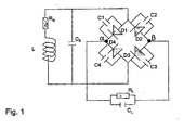
- Fig. 1 shows a typical circuit with four rectifying diodes D1-D4 used to rectify the voltage induced by the RF radiation in an inductive coil.
- the load circuit connected to the antenna has of course a capacitance associated with it, which normally needs to be taken into account when choosing the value of the capacitor C s .
- the load capacitance is sufficiently large that C s can be omitted altogether.
- the load capacitance should normally not be so large that is no longer possible to fulfill the resonance conditions without having to severely decrease the inductance L.
- the conductor of the RF antenna has a series resistance R 6 , which typically is less than 100-1000 ⁇ in order to achieve an antenna with sufficiently high quality factor.
- the diode circuit rectifies the AC voltage such that the voltage difference between points ⁇ and ⁇ of the bridge rectifier circuit is approximately constant, and can be used to provide the DC power supply for the operation of a logic circuit integrated onto the tag.
- the logic circuit might approximately be represented by a load resistance R L and a load capacitance C L . This and other configurations for the diode rectification circuitry are known in the prior art.
- solution-processible semiconducting materials such as molecular or conjugated polymer semiconductors
- printable metals such as conducting polymers, colloidal or precursor based inorganic metals
- solution-coatable dielectrics Thin-film deposition and patterning of these materials can be achieved by techniques such as inkjet printing, screen printing, flexographic printing, offset printing, aerosol deposition, spray coating, blade coating, spin coating, or dip coating.
- Rectifying diodes based on semiconducting conjugated polymers have been demonstrated (see for example, L. S. Roman, et al., APT 75. 3557 (1999 )) in the prior art. They are formed by incorporating a thin film of polymer 3 into a sandwich structure between two conducting electrodes, anode 2 and cathode 4. respectively ( Fig. 2B ). Rectification is normally obtained if the work functions of the anode and cathode are different, resulting in a built-in electrical field in the semiconducting polymer.
- the metal work function and the ionisation potential and electron affinity, respectively of the polymer semiconductor determine the energy barriers for charge injection of holes and electrons at the metal-semiconductor contacts, respectively.
- Diodes with high rectification are often fabricated by using materials that allow efficient charge injection from the metal electrode(s) into the semiconducting polymer under forward bias, but not under reverse bias.
- this is achieved by adjusting the work function of the anode to be close to the ionisation potential of the (p-type) semiconductor, but fabricating the cathode from a material that has a significant barrier for hole injection to suppress current flow under reverse bias.
- anode and cathode are chosen such that they provide efficient injection of holes and electrons, respectively, under forward bias, but represent significant injection barriers for the other type of carrier under reverse bias ( Fig. 2A ).
- Rectifying diodes based on semiconducting polymers have been fabricated with anodes based on high workfunction inorganic metals such as indium tin oxide or gold, and conducting polymers, such as PEDOT/PSS, and low workfunction cathodes, such as aluminum or calcium.
- the low-workfuncuon cathode material was deposited by vacuum deposition. It was found that the use of a conducting polymer layer, such as poly(ethylene dioxythiophene) doped with poly(styrene sulphonic acid) (PEDOT/PSS) as anode material improves the rectification ratio of the diodes significantly ( L. S. Roman, et al., APL, 75, 3557 (1999 )).
- PCT/NO00/0012 a method for fabrication of an organic thin-film diode and transistors is described, which is based on thermal evaporation of metal electrodes, and spin coating of organic layers.
- liquid processing e.g. direct printing
- US2003/0059987 describes a technique of using ink-jet printing to form an integrated circuit including at least two interconnected electronic switching device.
- rectifying diodes based on molecular or polymer semiconductors can be fabricated by solution processing and direct printing techniques that provide good rectification not only at DC frequencies, but also radiofrequencies by reducing the geometric overlap capacitance of the diode while maintaining or enhancing its forward current density,
- Figure 3 illustrates a method that allows fabrication of a rectifying diode with a low capacitance and a high forward current density by direct printing with small capacitance, high forward current density, and high rectification ratio at frequencies exceeding 100 kHz.
- the method is based on reducing the geometric overlap capacitance between the anode and cathode of the diode by fabricating the diode in a planar configuration with anode and cathode defined on the same level of the substrate, and closely spaced from another.
- the semiconducting layer deposited is deposited in contact with the two electrodes.
- the capacitance between anode and cathode is determined by the geometric overlap area between the two electrodes, and can be minimized simply by reducing the thickness of the two electrodes.
- the electrodes Preferably, the electrodes have a thickness smaller than the thickness of the semiconducting layer.
- the two electrode materials are deposited from solution by an additive printing technique.
- Anode and cathode can be fabricated from different conducting materials with different metal work function.
- the anode preferably has a higher workfunction than the cathode.
- the anode material is fabricated from a solution processible metal with a high workfunction, such as the conducting polymers PEDOT/PSS, polypyrrole, or polyaniline, or an inorganic metal, such as dispersion of inorganic metal nanoparticles or a chemical precursor solution of gold, palladium, nickel or platinum.
- a preferred choice for the anode material is the conducting polymer PEDOT/PSS
- the cathode is fabricated from a solution-processible low work function metal such as a dispersion of inorganic metal nanoparticles or a chemical precursor solution of silver.
- the anode and cathode material are deposited from the same material, but one of the electrodes is subjected to a selective surface treatment modifying the surface electronic properties of one electrode with respect to the other electrode resulting in rectifying behaviour of the diode.
- one of the two electrodes is deposited first and subjected to the surface treatment prior to the deposition of the second electrode.
- the surface treatment may consist of a chemical surface modification by deposition of a surface modifying agent, such as a self-assembled monolayer or a surfactant.
- the surface treatment may be a physical or physico-chemical treatment such as exposure to a plasma treatment, for example, a CF 4 or an oxygen plasma treatment.
- the ink used for the deposition of one of the two electrodes material might also contain an additive that modifies the electronic properties of one of the deposited metals, for example, increases or decreases its workfunction.
- An example of such an additive is a surfactant with a tendency to segregate to the surface and modify the electronic properties of the surface, i.e. to alter the injection characteristics of the electrode.
- a high forward current density of the diode can be achieved by arranging that at least one of the two electrodes provides efficient Ohmic charge injection of majority carriers into the semiconductor.
- Many conjugated polymers such as poly(3-hexylthiophene) (P3HT) or poly(dioctylfluorene-co-bithiophene) (F8T2) are slightly p-type doped; and the hole mobility is higher than the electron mobility.
- P3HT poly(3-hexylthiophene)
- F8T2 poly(dioctylfluorene-co-bithiophene)
- the distance between anode and cathode is smaller than 1 ⁇ m, most preferably smaller than 100 nm in order to achieve a high forward current.
- the distance between anode and cathode is smaller than 1 ⁇ m, most preferably smaller than 100 nm in order to achieve a high forward current.
- Various techniques can be used to define the small gap between source and drain, such as UV photolithography, screen printing, gravure, offset and flexographic printing.
- the electrodes of the planar rectifying diode are fabricated by a self-aligned printing technique, as described in WO03/056641 .
- the surface of a first printed electrode 10 is modified in such a way as to provide a surface energy pattern 11 to repel the ink of a second printed electrode 12.
- the surface modification can either be performed automatically during the printing of the first electrode, for example by mixing the ink of the first electrode material with a surfactant molecule, or by post-deposition surface modification, for example by exposure of the first electrode to a CF 4 plasma treatment prior to deposition of the second electrode.
- the self-aligned printing technique is capable of defining very small gaps between the two deposited electrodes that can in principle be of molecular dimension, It allows fabrication of source and drain electrode of submicrometer channel transistors.
- the anode and cathode are fabricated by the self-aligned printing technique from essentially the same material, and the rectifying behaviour of the diode is brought about by selective surface modification of one of the two electrodes.
- the surface modification is performed on the first electrode prior to the deposition of the second electrode.
- the step of modifying the charge injecting properties of the electrode may be performed at the same time as the step of modifying the surface of the firstly deposited electrode to provide the repulsive properties for the deposition of the ink of the second electrode.
- the surface modification step may provide both the surface repulsion and the desired charge injection properties.
- the anode and cathode electrode are both formed from PEDOT/PSS.
- the surface is fluorinated by exposure to short CF 4 plasma treatment (250W, 15s).
- the second electrode is inkjet deposited.
- the ink droplets are repelled from the first electrode, and deposited in the bare glass regions of the substrate immediately adjacent to the first electrode, defining a very short gap (see Fig. 9(A)).
- Atomic force microscopy topographs show that the gap between the two electrodes is very narrow ( ⁇ 100nm), and cannot be detected by the AFM technique.
- the diode is completed by deposition of a semiconducting polymer film, such as P3HT or F8T2.
- PEDOT-F8T2-PEDOT devices fabricated in this way show clear rectifying behaviour.
- the current is lower when the first deposited (fluorinated) electrode is biased positive with respect to the second deposited electrode, i.e., the unmodified PEDOT electrode has better hole injection properties into F8T2.
- the self-aligned printing technique allows fabrication of very small gap structures ( ⁇ 100 nm) with high forward current density and low probability for electrical shorts, since the contact region between the two electrodes is essentially a line, and not an area as in conventional diode configurations.
- the geometric overlap capacitance between the two electrodes is very small. It is advantageous if the electrodes have a tapered topographic profile where the thickness is becoming smaller towards the gap between the two electrodes (see Fig. 3B). In such a case the thickness of the region of smallest contact distance, which determines the overlap capacitance, is very small.
- the current density between source and drain remains high provided that the conductance of the electrode material remains sufficient up to the tapered edge, such that charge injection into the semiconductor occurs near the point of closest contact.
- the first and second electrodes are fabricated from different conductive materials.
- the two conductive materials and their workfunctions are chosen such as to give efficient injection of holes at the anode, and/or electrons at the cathode.
- the first electrode is either chosen such that its surface is repulsive for the ink of the second electrode, i.e. the contact angle of the ink of the second material on the surface of the first materia! is larger than that on the bare substrate surface (5).
- the first electrode may also be modified prior to deposition of the second electrode in an analogous way as described above.
- a first electrode of PEDOT/PSS is inkjet deposited onto a glass substrate and modified by exposure to a CF 4 plasma treatment (250W, 15s).
- a second electrode of silver is inkjet deposited from a nanoparticle dispersion in water, or a water ethylene glycol mixture.
- the silver ink is repelled by the fluorinated surface of PEDOT.
- the deposited silver pattern is then annealed at a temperature of typically 125-200°C in order to increase the conductivity.
- the device is completed by deposition of a thin film (B) of F8T2 or P3HT with a film thickness of 30 nm. The device exhibits rectifying characteristics, the current is higher when a positive bias is applied to the PEDOT electrode with respect to the silver electrode.
- the process can also be performed by depositing the silver electrode first, and annealing it to a temperature of 125-200°C. Subsequently, the surface of the printed silver pattern can be modified by deposition of a self-assembled monolayer, such as an alkane-thiol or a fluoroalkane-thiol monolayer, in order to enhance the surface repulsion of the subsequently deposited PEDOT/PSS ink from the silver surface.
- Running the process in this sequence has the advantage that the silver electrode becomes insoluble in water during the annealing step reducing the risk for electrical shorts between the two electrodes.
- the surface modification layer is sufficiently dense, that the subsequently deposited ink does not start to redissolve the first electrode while it is coming in contact with the first electrode during the printing process. It is also possible to perform the self-aligned printing process with two inorganic metal electrodes, such as silver or gold.
- the first electrode can be surface modified with a self-assembled monolayer prior to deposition of the second electrode.
- the second electrode can be modified separately with a second self-assembled monolayer.
- the first electrode is chemically passivated, and will not be modified by the second self-assembled monolayer. This allows fine-tuning separately the charge injection characteristics of the two electrodes.
- the simplest equivalent circuit diagram to represent a rectifying diode consists of a parallel combination of a capacitor C d (representing, in the simplest case the geometric capacitance of an undoped semiconducting polymer layer sandwiched between anode and cathode), and a nonlinear resistor.
- C d representing, in the simplest case the geometric capacitance of an undoped semiconducting polymer layer sandwiched between anode and cathode
- R Rev (V rev ) and R Forw (V Forw ) be the resistance of the diode under reverse and forward bias, respectively.
- Typical polymer diodes fabricated in the prior art have a thickness on the order of 100 nm, and a dielectric constant on the order of 3.5, corresponding to a capacitance on the order of 30nF/cm 2 .
- the typical forward current density of a polymer diode is on the order of o,1A/cm 2 at a voltage of 10V. This implies that the forward bias impedance of the diode is on the order of 100 ⁇ /cm 2 .
- the forward current density of the rectifying diode needs to be sufficiently high to allow supplying the total current I s that is drawn from the power supply by the logic circuit of the tag.
- I s is typically on the order of 100 ⁇ A -1 mA for a p-type logic circuit containing 1000-10000 gates constituting a typical load resistance on the order of 10k ⁇ - 1k ⁇ .
- the required current supplied by the diode can be achieved by adjusting the area/width of the rectifying diode.
- the forward current density of the rectifying diodes also needs to be able to charge the load capacitance C L of the logic circuit within a sufficiently fast time scale. It is not necessary that the load capacitance is charged fully within a single period of the RF wave, but the DC bias can be built up over several periods. However, the smaller the forward current density, the longer it will take before the DC bias generated by the diodes is available as power supply to the tag.
- the semiconducting layer is fabricated preferably from a material with high charge carrier mobility, for at least one of the electron and hole carriers, most preferably for both carriers.
- a unipolar device where the current is carried mainly by one type of carrier the space charge limited current flowing in the device is the larger the higher the mobility of the semiconductor.
- a bipolar device where both electrons and holes can be injected from the respective electrodes under forward bias, the forward current can be even higher than the space charge limited current of the respective unipolar device due to partial compensation of the space charge of one carrier by the space charge of the other carrier.
- a high charge carrier mobility is also required to ensure that the diode current responds to the applied AC bias.
- the mobility ⁇ of charge carriers carrying the current in the diode of thickness d, to which a voltage V is applied needs to be sufficiently high to allow modulation of the current with the required frequency f , i , e ⁇ ⁇ • V • ⁇ 2 d 2 > ⁇ RF .
- the semiconducting material may also be a blend of two or more components, for example, a blend of a hole transporting polymer such as P3HT, polyfluorene derivatives such as F8T2, or polyphenylene vinylene derivatives and an electron transporting polymer, such as poly(dioctylfluorene-co-benzothiadiazole) (F8BT).
- a hole transporting polymer such as P3HT
- polyfluorene derivatives such as F8T2
- polyphenylene vinylene derivatives such as poly(dioctylfluorene-co-benzothiadiazole) (F8BT).
- F8BT poly(dioctylfluorene-co-benzothiadiazole)
- the anode material is fabricated from a solution processible metal with a high workfunction, such as the conducting polymers PEDOT/PSS. polythiophene, polypyrrole, or polyaniline, or an inorganic metal, such as dispersion of inorganic metal nanoparticles or a chemical precursor solution of gold, palladium, nickel or platinum.
- a preferred choice for the anode material is the conducting polymer PEDOT/PSS.
- the cathode is fabricated from a solution processible low work function metal such as dispersion of inorganic metal nanoparticles or a chemical precursor solution.
- a suitable metal with reasonably low workfunction, and adequate stability is silver.
- the work function of a material can be obtained using electrical or chemical surface energy modification.
- the modification could be performed either before or after deposition of the semi-conducting layer or layers i.e. either of the electrodes, or indeed the substrate or semi-conducting layer(s), could be modified to induce electronic or chemical differences between the injection properties of electrodes.
- the use of different solvents or different solvent ratios for ink formation may also induce sufficient differences between electrodes of the same material such that diode behaviour is achieved.
- altering the proportion of glycerol to water in a PEDOT:PSS suspension induces rectifying behaviour in a diode with both PEDOT/PSS anode and cathode electrodes.
- diodes are also useful for multiplying the DC voltage that arises from an ac induced voltage. This is of particular importance to plastic electronics compared to silicon, since the TFTs tend to operate with higher voltages and lower currents than silicon.
- the diode devices described above can be used in different rectifier configurations, including but not limited to, the bridge rectifier shown in Fig. 1 , or the Villard cascade or charge pump shown in Fig- 11A.
- the latter both rectifies and multiplies the ac voltage. This is beneficial as organic transistor circuits require relatively large supply voltages of typically 5-40V for their operation.
- the DC output voltage of a Villard cascade is up to n times lager, where n is the number of stages in the ladder. Naturally this is at the expense of the available current.
- the processes and devices described herein are not limited to devices fabricated with solution-processed polymers.
- some of the conducting electrodes and/or the interconnects may be formed from inorganic conductors, that can, for example, be deposited by printing of a colloidal suspension or by electroplating onto a pre-patterned substrate.
- inorganic conductors that can, for example, be deposited by printing of a colloidal suspension or by electroplating onto a pre-patterned substrate.
- one or more layers of the device may be replaced with a vacuum deposited material, such as for example vacuum deposited pentacene.
- One of more layers of the device might also be patterned by conventional photolithographic techniques.
- any solution processible conjugated polymeric or oligomeric material that exhibits adequate field-effect mobilities exceeding 10 -3 cm 2 /Vs, preferably exceeding 10 -2 cm 2 /Vs, may be used. Suitable materials are reviewed for example in H.E. Katz, J. Mater. Chem. 7, 369 (1997 ), or Z. Bao, Advanced Materials 12, 227 (2000 ). Other possibilities include small conjugated molecules with solubilising side chains ( J.G. Laquindanum, et al., J. Am. Chem. Soc. 120, 664 (1998 )), semiconducting organic-inorganic hybrid materials self-assembled from solution ( C.R. Kagan, et al., Science 286, 946 (1999 )), or solution-deposited inorganic semiconductors such as CdSe nanoparticles ( B. A. Ridley, et al., Science 286, 746 (1999 )).
- the electrodes may be coarse-patterned by techniques other than inkjet printing. Suitable techniques include soft lithographic printing ( J.A. Rogers et al., Appl. Phys. Lett. 75, 1010 (1999 ); S. Brittain et al., Physics World May 1998, p. 31 ), screen printing ( Z. Bao, et al., Chem. Mat. 9, 12999 (1997 )), and photolithographic patterning (see WO 99/10939 ), offset printing, flexographic printing or other graphic arts printing techniques, lnk-jet printing is considered to be particularly suitable for large area patterning with good registration, in particular for flexible plastic substrates.
- one or more components may also be deposited by vacuum deposition techniques and/or patterned by a photolithographic process.
- Devices such as rectifying diodes fabricated as described above may be part of a more complex circuit or device in which one or more such devices can be integrated with each other and or with other devices.
- Examples of applications include logic circuits and active matrix circuitry for a display or a memory device, or a user-defined gate array circuit.
- the patterning process may be used to pattern other components of such circuit as well, such as interconnects, resistors, capacitors etc.
- the present invention is not limited to the foregoing examples.
Landscapes
- Engineering & Computer Science (AREA)
- Chemical & Material Sciences (AREA)
- Nanotechnology (AREA)
- Manufacturing & Machinery (AREA)
- Physics & Mathematics (AREA)
- Composite Materials (AREA)
- Condensed Matter Physics & Semiconductors (AREA)
- General Physics & Mathematics (AREA)
- Materials Engineering (AREA)
- Crystallography & Structural Chemistry (AREA)
- Electrodes Of Semiconductors (AREA)
- Bipolar Transistors (AREA)
- Amplifiers (AREA)
Abstract
Description
- This invention relates to rectifying diode devices and their fabrication, and in particular to rectifying diodes preparable by solution processing and direct printing techniques, and methods for their fabrication.
- A rectifying diode, i.e. a two-terminal device with asymmetric, nonlinear current-voltage characteristics, is an important element of many electronic circuits. Diodes can be used, for example, as nonlinear circuit elements that provide signal mixing capability. They allow generating an output signal at a frequency different from that of the input signal, for example, generation of signals at twice the input frequency, or generation of frequencies at the sum frequency ω1+ω2 or the difference frequency ω1-ω2 from two input signals at ω1 and ω2. This is important for radiofrequency (RF) communication and tagging applications, where communication between a contactless tag and a base station is established by emission of an RF signal with a given frequency, such as 125 kHz or 13.56 MHz, that is absorbed in an RF antenna coil on the tag. Higher sensitivities and immunity to noise can be achieved if the response of the tag is not at the same frequency, but at a frequency shifted from that of the signal emitted by the base station.
- An important function for a rectifying diode in an RF identification (RFID) tag can be to provide the rectifying element that is used to rectify the AC voltage induced in the RF antenna and covert it into a DC voltage signal that is capable of providing the DC power to the logic circuit integrated on the tag.
Fig. 1 shows a typical circuit with four rectifying diodes D1-D4 used to rectify the voltage induced by the RF radiation in an inductive coil. - In most applications a resonance circuit is formed between the inductor L and a capacitor Cs, such that the resonance frequency ω= 1/LCs is close to the frequency of the RF radiation to be absorbed. Note that the load circuit connected to the antenna has of course a capacitance associated with it, which normally needs to be taken into account when choosing the value of the capacitor Cs. In some cases the load capacitance is sufficiently large that Cs can be omitted altogether. However, the load capacitance should normally not be so large that is no longer possible to fulfill the resonance conditions without having to severely decrease the inductance L.
- The conductor of the RF antenna has a series resistance R6, which typically is less than 100-1000 Ω in order to achieve an antenna with sufficiently high quality factor. The diode circuit rectifies the AC voltage such that the voltage difference between points α and β of the bridge rectifier circuit is approximately constant, and can be used to provide the DC power supply for the operation of a logic circuit integrated onto the tag. The logic circuit might approximately be represented by a load resistance RL and a load capacitance CL. This and other configurations for the diode rectification circuitry are known in the prior art.
- There is currently growing interest in manufacturing of integrated electronic circuits by solution processing and additive printing techniques, that enable fabrication of electronic circuits on large areas and on flexible, plastic substrates at low-cost, This technology is based on (a) solution-processible semiconducting materials such as molecular or conjugated polymer semiconductors, (b) printable metals, such as conducting polymers, colloidal or precursor based inorganic metals and (c) solution-coatable dielectrics. Thin-film deposition and patterning of these materials can be achieved by techniques such as inkjet printing, screen printing, flexographic printing, offset printing, aerosol deposition, spray coating, blade coating, spin coating, or dip coating.
- Rectifying diodes based on semiconducting conjugated polymers have been demonstrated (see for example, L. S. Roman, et al., APT 75. 3557 (1999)) in the prior art. They are formed by incorporating a thin film of
polymer 3 into a sandwich structure between two conducting electrodes,anode 2 andcathode 4. respectively (Fig. 2B ). Rectification is normally obtained if the work functions of the anode and cathode are different, resulting in a built-in electrical field in the semiconducting polymer. The metal work function and the ionisation potential and electron affinity, respectively of the polymer semiconductor determine the energy barriers for charge injection of holes and electrons at the metal-semiconductor contacts, respectively. - Diodes with high rectification are often fabricated by using materials that allow efficient charge injection from the metal electrode(s) into the semiconducting polymer under forward bias, but not under reverse bias. In the case of a unipolar device, where the current is carried by only one type of carriers, for example holes, this is achieved by adjusting the work function of the anode to be close to the ionisation potential of the (p-type) semiconductor, but fabricating the cathode from a material that has a significant barrier for hole injection to suppress current flow under reverse bias. In a bipolar device, where both electrons and holes contribute to the current, anode and cathode, respectively, are chosen such that they provide efficient injection of holes and electrons, respectively, under forward bias, but represent significant injection barriers for the other type of carrier under reverse bias (
Fig. 2A ). - Rectifying diodes based on semiconducting polymers have been fabricated with anodes based on high workfunction inorganic metals such as indium tin oxide or gold, and conducting polymers, such as PEDOT/PSS, and low workfunction cathodes, such as aluminum or calcium. The low-workfuncuon cathode material was deposited by vacuum deposition. It was found that the use of a conducting polymer layer, such as poly(ethylene dioxythiophene) doped with poly(styrene sulphonic acid) (PEDOT/PSS) as anode material improves the rectification ratio of the diodes significantly (L. S. Roman, et al., APL, 75, 3557 (1999)). In
PCT/NO00/0012 - The methods for polymer-based rectifying diodes that are disclosed in the prior art do not allow fabrication of rectifying diodes by direct printing techniques nor do they allow operation of these diodes at radio frequencies for the following reasons,
- 1. Use of inorganic metals deposited by vacuum evaporation: The prior art is based on the use of inorganic metals for anode and, in particular, for cathode electrodes. The materials are deposited by vacuum deposition and are patterned by techniques such as photolithography or shadow mask evaporation. Although solution processible conducting polymers, such as PEDOT/PSS. have been used successfully for anode fabrication (L. S. Roman, et al., APL, 75. 3557 (1999)) while the low workfunction cathode was a vacuum sublimed inorganic metal.
- 2. Environmental stability: Rectifying diodes based on low-workfunction metal cathodes such as calcium need to be encapsulated carefully in order to prevent oxidation of the cathode by exposure to the atmosphere. The need for high-performance encapsulation is acceptable for some applications such as polymer fight-emitting diode displays. However, for many low-cost applications of printed integrated circuits, the need to encapsulate the device would add intolerable manufacturing cost. For these applications it is not tolerable, that the cathode material of only a few diode elements in the circuit determines the encapsulation requirements while the other elements of the circuit, such as for example transistor elements, would require much less sophisticated encapsulation to achieve the desired reliability.
- 3. Process complexity: The rectifying diode will typically form part of an integrated circuit comprising other devices such as transistors. Polymer transistors are usually fabricated in multilayer structures with source and drain electrodes located on one level of the device, and the gate electrodes located on different level. However, it is possible to fabricate source-drain and gate electrode from the same, high-work function material, simplifying the manufacturing process. It would be highly desirable if rectifying diodes could also be fabricated with anode and cathode fabricated from essentially the same material.
- 4. Loss of rectification ratio at high frequencies: When a polymer diode fabricated according to the prior art and exhibiting a high DC rectification ratio is operated at high frequencies of 125 kHz or 13.56 MHz a decrease of the rectification ratio is observed. At 13.56 MHz most polymer diodes according to the prior art lose their rectification behaviour almost fully.
- It is an aim of the present invention to provide a diode that can be produced by liquid processing (e.g. direct printing) and that can be used for rectification at radio frequencies.
-
US2003/0059987 describes a technique of using ink-jet printing to form an integrated circuit including at least two interconnected electronic switching device. - According to the present invention, there is provided a method for fabricating a rectifying diode according to
claim 1. - Optional preferred features are recited In
claims 2 to 7. - With the method of forming electrodes recited In the claims, rectifying diodes based on molecular or polymer semiconductors can be fabricated by solution processing and direct printing techniques that provide good rectification not only at DC frequencies, but also radiofrequencies by reducing the geometric overlap capacitance of the diode while maintaining or enhancing its forward current density,
- Preferred embodiments of the invention will now be described, by way of example only, with reference to the accompanying drawings, in which::
-
Figure 1 shows a schematic equivalent circuit of a RF antenna comprising a bridge of rectifying diodes to generate a DC voltage supply for a load device coupled to the antenna. -
Figure 2 shows a schematic energy diagram (A) and layer structure (B) for a polymer rectifying diode. -
Figure 3 shows an in-plane rectifying diode with a small capacitance with self-aligned, laterally offset anode and cathode electrodes produced according to an embodiment of the present invention. -
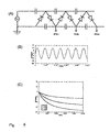
Figure 4 shows a circuit diagram of a three-stage Viilard cascade charge pump (A) and corresponding circuit simulation (B,C). -
Figure 3 illustrates a method that allows fabrication of a rectifying diode with a low capacitance and a high forward current density by direct printing with small capacitance, high forward current density, and high rectification ratio at frequencies exceeding 100 kHz. The method is based on reducing the geometric overlap capacitance between the anode and cathode of the diode by fabricating the diode in a planar configuration with anode and cathode defined on the same level of the substrate, and closely spaced from another. The semiconducting layer deposited is deposited in contact with the two electrodes. In a planar rectifying diode the capacitance between anode and cathode is determined by the geometric overlap area between the two electrodes, and can be minimized simply by reducing the thickness of the two electrodes. Preferably, the electrodes have a thickness smaller than the thickness of the semiconducting layer. Preferably the two electrode materials are deposited from solution by an additive printing technique. - Anode and cathode can be fabricated from different conducting materials with different metal work function. The anode preferably has a higher workfunction than the cathode. The anode material is fabricated from a solution processible metal with a high workfunction, such as the conducting polymers PEDOT/PSS, polypyrrole, or polyaniline, or an inorganic metal, such as dispersion of inorganic metal nanoparticles or a chemical precursor solution of gold, palladium, nickel or platinum. A preferred choice for the anode material is the conducting polymer PEDOT/PSS, The cathode is fabricated from a solution-processible low work function metal such as a dispersion of inorganic metal nanoparticles or a chemical precursor solution of silver.
- According to one technique not in accordance with the claimed invention, the anode and cathode material are deposited from the same material, but one of the electrodes is subjected to a selective surface treatment modifying the surface electronic properties of one electrode with respect to the other electrode resulting in rectifying behaviour of the diode. Preferably, one of the two electrodes is deposited first and subjected to the surface treatment prior to the deposition of the second electrode. The surface treatment may consist of a chemical surface modification by deposition of a surface modifying agent, such as a self-assembled monolayer or a surfactant. Alternatively, the surface treatment may be a physical or physico-chemical treatment such as exposure to a plasma treatment, for example, a CF4 or an oxygen plasma treatment. The ink used for the deposition of one of the two electrodes material might also contain an additive that modifies the electronic properties of one of the deposited metals, for example, increases or decreases its workfunction. An example of such an additive is a surfactant with a tendency to segregate to the surface and modify the electronic properties of the surface, i.e. to alter the injection characteristics of the electrode.
- A high forward current density of the diode can be achieved by arranging that at least one of the two electrodes provides efficient Ohmic charge injection of majority carriers into the semiconductor. Many conjugated polymers, such as poly(3-hexylthiophene) (P3HT) or poly(dioctylfluorene-co-bithiophene) (F8T2) are slightly p-type doped; and the hole mobility is higher than the electron mobility. For such a polymer semiconductor, it is preferred to choose an anode material the workfunction of which is well matched to the ionisation potential of the semiconducting material, in order to achieve the maximum space-charge limited current density that is possible in a unipolar device under forward bias. Even higher current densities can be achieved by also forming an Ohmic or quasi-Ohmic contact at the electron injecting cathode, by choosing a cathode material with a work function close to the electron affinity of the semiconducting material. In this case the positive space charge of the injected holes can be partially compensated by injected electron space charge.
- Preferably, the distance between anode and cathode is smaller than 1µm, most preferably smaller than 100 nm in order to achieve a high forward current. For a planar diode this requires a high-resolution patterning step. Various techniques can be used to define the small gap between source and drain, such as UV photolithography, screen printing, gravure, offset and flexographic printing.
- According to an embodiment of the claimed invention, the electrodes of the planar rectifying diode are fabricated by a self-aligned printing technique, as described in
WO03/056641 electrode 10 is modified in such a way as to provide asurface energy pattern 11 to repel the ink of a second printedelectrode 12. The surface modification can either be performed automatically during the printing of the first electrode, for example by mixing the ink of the first electrode material with a surfactant molecule, or by post-deposition surface modification, for example by exposure of the first electrode to a CF4 plasma treatment prior to deposition of the second electrode. The self-aligned printing technique is capable of defining very small gaps between the two deposited electrodes that can in principle be of molecular dimension, It allows fabrication of source and drain electrode of submicrometer channel transistors. - According to one technique not in accordance with the claimed invention, the anode and cathode are fabricated by the self-aligned printing technique from essentially the same material, and the rectifying behaviour of the diode is brought about by selective surface modification of one of the two electrodes. Preferably, the surface modification is performed on the first electrode prior to the deposition of the second electrode. The step of modifying the charge injecting properties of the electrode may be performed at the same time as the step of modifying the surface of the firstly deposited electrode to provide the repulsive properties for the deposition of the ink of the second electrode. In one embodiment, the surface modification step may provide both the surface repulsion and the desired charge injection properties. In one embodiment, the anode and cathode electrode are both formed from PEDOT/PSS. After inkjet deposition of the first PEDOT electrode onto a borosilicate glass substrate the surface is fluorinated by exposure to short CF4 plasma treatment (250W, 15s). Afterwards the second electrode is inkjet deposited. The ink droplets are repelled from the first electrode, and deposited in the bare glass regions of the substrate immediately adjacent to the first electrode, defining a very short gap (see Fig. 9(A)). Atomic force microscopy topographs show that the gap between the two electrodes is very narrow (< 100nm), and cannot be detected by the AFM technique. Finally, the diode is completed by deposition of a semiconducting polymer film, such as P3HT or F8T2. PEDOT-F8T2-PEDOT devices fabricated in this way show clear rectifying behaviour. The current is lower when the first deposited (fluorinated) electrode is biased positive with respect to the second deposited electrode, i.e., the unmodified PEDOT electrode has better hole injection properties into F8T2.
- The self-aligned printing technique allows fabrication of very small gap structures (<100 nm) with high forward current density and low probability for electrical shorts, since the contact region between the two electrodes is essentially a line, and not an area as in conventional diode configurations. The geometric overlap capacitance between the two electrodes is very small. It is advantageous if the electrodes have a tapered topographic profile where the thickness is becoming smaller towards the gap between the two electrodes (see Fig. 3B). In such a case the thickness of the region of smallest contact distance, which determines the overlap capacitance, is very small. The current density between source and drain remains high provided that the conductance of the electrode material remains sufficient up to the tapered edge, such that charge injection into the semiconductor occurs near the point of closest contact.
- The first and second electrodes are fabricated from different conductive materials. The two conductive materials and their workfunctions are chosen such as to give efficient injection of holes at the anode, and/or electrons at the cathode. The first electrode is either chosen such that its surface is repulsive for the ink of the second electrode, i.e. the contact angle of the ink of the second material on the surface of the first materia! is larger than that on the bare substrate surface (5). Alternatively, the first electrode may also be modified prior to deposition of the second electrode in an analogous way as described above. According to one example, a first electrode of PEDOT/PSS is inkjet deposited onto a glass substrate and modified by exposure to a CF4 plasma treatment (250W, 15s). Then a second electrode of silver is inkjet deposited from a nanoparticle dispersion in water, or a water ethylene glycol mixture. The silver ink is repelled by the fluorinated surface of PEDOT. The deposited silver pattern is then annealed at a temperature of typically 125-200°C in order to increase the conductivity. The device is completed by deposition of a thin film (B) of F8T2 or P3HT with a film thickness of 30 nm. The device exhibits rectifying characteristics, the current is higher when a positive bias is applied to the PEDOT electrode with respect to the silver electrode.
- The process can also be performed by depositing the silver electrode first, and annealing it to a temperature of 125-200°C. Subsequently, the surface of the printed silver pattern can be modified by deposition of a self-assembled monolayer, such as an alkane-thiol or a fluoroalkane-thiol monolayer, in order to enhance the surface repulsion of the subsequently deposited PEDOT/PSS ink from the silver surface. Running the process in this sequence has the advantage that the silver electrode becomes insoluble in water during the annealing step reducing the risk for electrical shorts between the two electrodes. If the PEDOT is deposited first, case needs to be taken that the surface modification layer is sufficiently dense, that the subsequently deposited ink does not start to redissolve the first electrode while it is coming in contact with the first electrode during the printing process. It is also possible to perform the self-aligned printing process with two inorganic metal electrodes, such as silver or gold.
- In all cases the first electrode can be surface modified with a self-assembled monolayer prior to deposition of the second electrode. Afterwards the second electrode can be modified separately with a second self-assembled monolayer. By then the first electrode is chemically passivated, and will not be modified by the second self-assembled monolayer. This allows fine-tuning separately the charge injection characteristics of the two electrodes.
- The simplest equivalent circuit diagram to represent a rectifying diode consists of a parallel combination of a capacitor Cd (representing, in the simplest case the geometric capacitance of an undoped semiconducting polymer layer sandwiched between anode and cathode), and a nonlinear resistor. Let RRev(Vrev) and RForw(VForw) be the resistance of the diode under reverse and forward bias, respectively. When an alternating voltage is applied to the diode, the current will flow through the capacitance, i.e. will not experience rectification, if the resistance of the diode Is larger than the impedance of the capacitor. Typical polymer diodes fabricated in the prior art have a thickness on the order of 100 nm, and a dielectric constant on the order of 3.5, corresponding to a capacitance on the order of 30nF/cm2. This implies an impedance Zc = 1/ωC = 0.4 Ω/cm2 (13.56 MHz) and 42 Ω/cm2(125 kHz). On the other hand the typical forward current density of a polymer diode is on the order of o,1A/cm2 at a voltage of 10V. This implies that the forward bias impedance of the diode is on the order of 100 Ω/cm2. This is larger than that of the capacitance, meaning that even under forward bias the AC current will flow through the capacitor, and not the rectifying diode. Under reverse bias the diode resistance is even higher and the current will also flow through the capacitor. Therefore, a polymer diode of the prior art exhibits no rectification at high frequencies of 13.56 MHz (125 kHz). The key to achieving rectification at high frequencies is to ensure that the forward bias resistance RF is sufficiently small, that under forward bias the AC current is not also flowing through the capacitor, i.e. 1/RF·C > VRF. It is not necessary that the DC rectification ratio of the diode is higher than typically 100.
- The forward current density of the rectifying diode needs to be sufficiently high to allow supplying the total current Is that is drawn from the power supply by the logic circuit of the tag. Is is typically on the order of 100µA -1 mA for a p-type logic circuit containing 1000-10000 gates constituting a typical load resistance on the order of 10kΩ - 1kΩ. The required current supplied by the diode can be achieved by adjusting the area/width of the rectifying diode.
- The forward current density of the rectifying diodes also needs to be able to charge the load capacitance CL of the logic circuit within a sufficiently fast time scale. It is not necessary that the load capacitance is charged fully within a single period of the RF wave, but the DC bias can be built up over several periods. However, the smaller the forward current density, the longer it will take before the DC bias generated by the diodes is available as power supply to the tag.
- For all of the above methods the semiconducting layer is fabricated preferably from a material with high charge carrier mobility, for at least one of the electron and hole carriers, most preferably for both carriers. In a unipolar device where the current is carried mainly by one type of carrier the space charge limited current flowing in the device is the larger the higher the mobility of the semiconductor. In a bipolar device, where both electrons and holes can be injected from the respective electrodes under forward bias, the forward current can be even higher than the space charge limited current of the respective unipolar device due to partial compensation of the space charge of one carrier by the space charge of the other carrier.
- A high charge carrier mobility is also required to ensure that the diode current responds to the applied AC bias. The mobility µ of charge carriers carrying the current in the diode of thickness d, to which a voltage V is applied needs to be sufficiently high to allow modulation of the current with the required frequency

- The semiconducting material may also be a blend of two or more components, for example, a blend of a hole transporting polymer such as P3HT, polyfluorene derivatives such as F8T2, or polyphenylene vinylene derivatives and an electron transporting polymer, such as poly(dioctylfluorene-co-benzothiadiazole) (F8BT). In this case the electron and hole transporting properties can be optimized separately for the two polymers. The phase separation of the two polymers needs to be controlled to form a bicontinuous network.
- Examples of suitable additive printing techniques for the deposition of the electrodes and semiconducting layer are, but not limited to, inkjet printing, screen printing, stencil printing, offset, gravure and flexographic printing. The anode material is fabricated from a solution processible metal with a high workfunction, such as the conducting polymers PEDOT/PSS. polythiophene, polypyrrole, or polyaniline, or an inorganic metal, such as dispersion of inorganic metal nanoparticles or a chemical precursor solution of gold, palladium, nickel or platinum. A preferred choice for the anode material is the conducting polymer PEDOT/PSS. The cathode is fabricated from a solution processible low work function metal such as dispersion of inorganic metal nanoparticles or a chemical precursor solution. A suitable metal with reasonably low workfunction, and adequate stability is silver.
- Further rectification can be obtained upon optimisation of the work function of electrodes in order to control injection of carriers. The work function of a material can be obtained using electrical or chemical surface energy modification. The modification could be performed either before or after deposition of the semi-conducting layer or layers i.e. either of the electrodes, or indeed the substrate or semi-conducting layer(s), could be modified to induce electronic or chemical differences between the injection properties of electrodes.
- The use of different solvents or different solvent ratios for ink formation may also induce sufficient differences between electrodes of the same material such that diode behaviour is achieved. For example, altering the proportion of glycerol to water in a PEDOT:PSS suspension induces rectifying behaviour in a diode with both PEDOT/PSS anode and cathode electrodes.
- In an RFID application, diodes are also useful for multiplying the DC voltage that arises from an ac induced voltage. This is of particular importance to plastic electronics compared to silicon, since the TFTs tend to operate with higher voltages and lower currents than silicon.
- The diode devices described above can be used in different rectifier configurations, including but not limited to, the bridge rectifier shown in
Fig. 1 , or the Villard cascade or charge pump shown in Fig- 11A. The latter both rectifies and multiplies the ac voltage. This is beneficial as organic transistor circuits require relatively large supply voltages of typically 5-40V for their operation. Compared to a conventional bridge rectifier, the DC output voltage of a Villard cascade is up to n times lager, where n is the number of stages in the ladder. Naturally this is at the expense of the available current. - If too much current is drawn at the end of the cascade, some of the voltage is dropped across the capacitors and is therefore lost. The amount lost is given by the Villard formula:

- For a tag operating at frequency f = 125kHz that requires a dc voltage ∼40V to operate, and using typical diode properties as measured experimentally, capacitors of C = 8nF are required. For a three stage Villard cascade (n=3), and a current requirement of 100 µA. the voltage lost is ΔV=2V, so that for an initial 10V RF signal (Fig. 11B), an output of 40-2 = 38V and a 100 µA current can be obtained. This means that the tag needs to extract more than 4mW from the RF field. A simulation of the voltage build up at the output of the different stages of a 3-stage Villard cascade as a function of time is shown in Fig. 11C.
- The processes and devices described herein are not limited to devices fabricated with solution-processed polymers. For example, some of the conducting electrodes and/or the interconnects may be formed from inorganic conductors, that can, for example, be deposited by printing of a colloidal suspension or by electroplating onto a pre-patterned substrate. In devices in which not all layers are to be deposited from solution one or more layers of the device may be replaced with a vacuum deposited material, such as for example vacuum deposited pentacene. One of more layers of the device might also be patterned by conventional photolithographic techniques.
- For the semiconducting layer any solution processible conjugated polymeric or oligomeric material that exhibits adequate field-effect mobilities exceeding 10-3 cm2/Vs, preferably exceeding 10-2 cm2/Vs, may be used. Suitable materials are reviewed for example in H.E. Katz, J. Mater. Chem. 7, 369 (1997), or Z. Bao, ). Other possibilities include small conjugated molecules with solubilising side chains (J.G. Laquindanum, et al., J. Am. Chem. Soc. 120, 664 (1998)), semiconducting organic-inorganic hybrid materials self-assembled from solution (C.R. Kagan, et al., Science 286, 946 (1999)), or solution-deposited inorganic semiconductors such as CdSe nanoparticles (B. A. Ridley, et al., Science 286, 746 (1999)).
- The electrodes may be coarse-patterned by techniques other than inkjet printing. Suitable techniques include soft lithographic printing (J.A. Rogers et al., Appl. Phys. Lett. 75, 1010 (1999); S. Brittain et al., Physics World May 1998, p. 31), screen printing (Z. Bao, et al., Chem. Mat. 9, 12999 (1997)), and photolithographic patterning (see
WO 99/10939 - Although preferably all layers and components of the device and circuit are deposited and patterned by solution processing and printing techniques, one or more components may also be deposited by vacuum deposition techniques and/or patterned by a photolithographic process.
- Devices such as rectifying diodes fabricated as described above may be part of a more complex circuit or device in which one or more such devices can be integrated with each other and or with other devices. Examples of applications include logic circuits and active matrix circuitry for a display or a memory device, or a user-defined gate array circuit.
- The patterning process may be used to pattern other components of such circuit as well, such as interconnects, resistors, capacitors etc.
- The present invention is not limited to the foregoing examples.
- In view of the foregoing description it will be evident to a person skilled in the art that various modifications may be made within the scope of the claims.
Claims (7)
- A method for fabricating a rectifying diode including an active semiconducting layer between first and second electrodes, the method comprising:depositing from liquid the first electrode (10) comprising a first conductive material in a first region of a substrate (5),depositing a liquid comprising a second conductive material having a work function different to that of the first conductive material to come in contact with the first electrode and to form the second electrode (12) of the second conductive material in a second region of the substrate spaced from the first region,preparing the surface of the first electrode prior to the deposition of the liquid comprising the second material to repel the liquid, anddepositing semiconducting material (11) in the region between the first and second electrodes to form said active semiconducting layer,wherein the shortest distance between the first electrode and the second electrode defines the thickness of the active semiconducting layer of the rectifying diode.
- A method as claimed in any preceding claim wherein the surface of the first and second electrodes exhibit different workfunctions.
- A method as claimed in any preceding claim wherein said shortest distance between the first and second electrodes is less than 500 nm.
- A method as claimed in any preceding claim wherein said shortest distance between the first and second electrodes is less than 100 nm.
- A method as claimed in any preceding claim wherein said shortest distance between the first and second electrodes is less than 10 nm.
- A method as claimed in any preceding claim, wherein at least one of the first and second conductive materials is a conducting polymer.
- A method as claimed in any of claims 1 to 6, wherein at least one of the first and second conductive materials is a printable metal.
Applications Claiming Priority (2)
| Application Number | Priority Date | Filing Date | Title |
|---|---|---|---|
| GBGB0315477.0A GB0315477D0 (en) | 2003-07-02 | 2003-07-02 | Rectifying diodes |
| PCT/GB2004/002879 WO2005004194A2 (en) | 2003-07-02 | 2004-07-02 | Organic rectifying diodes |
Publications (2)
| Publication Number | Publication Date |
|---|---|
| EP1639659A2 EP1639659A2 (en) | 2006-03-29 |
| EP1639659B1 true EP1639659B1 (en) | 2011-11-02 |
Family
ID=27676516
Family Applications (1)
| Application Number | Title | Priority Date | Filing Date |
|---|---|---|---|
| EP04743225A Expired - Lifetime EP1639659B1 (en) | 2003-07-02 | 2004-07-02 | Method of fabricating organic rectifying diodes |
Country Status (5)
| Country | Link |
|---|---|
| US (1) | US7696090B2 (en) |
| EP (1) | EP1639659B1 (en) |
| AT (1) | ATE532223T1 (en) |
| GB (1) | GB0315477D0 (en) |
| WO (1) | WO2005004194A2 (en) |
Cited By (1)
| Publication number | Priority date | Publication date | Assignee | Title |
|---|---|---|---|---|
| WO2024115944A1 (en) * | 2022-11-29 | 2024-06-06 | Hossein Babaei Faramarz | Organic rectifying diode |
Families Citing this family (21)
| Publication number | Priority date | Publication date | Assignee | Title |
|---|---|---|---|---|
| GB0400997D0 (en) | 2004-01-16 | 2004-02-18 | Univ Cambridge Tech | N-channel transistor |
| DE102005009820A1 (en) | 2005-03-01 | 2006-09-07 | Polyic Gmbh & Co. Kg | Electronic assembly with organic logic switching elements |
| DE102005013125B4 (en) * | 2005-03-18 | 2008-12-18 | O-Flexx Technologies Gmbh | Process for the production of electronic units in a multilayer starting structure and use of this starting structure in the process |
| KR101317695B1 (en) * | 2005-05-09 | 2013-10-15 | 나노 이프린트 리미티드 | Electronic devices |
| US20080203384A1 (en) * | 2005-07-27 | 2008-08-28 | Koninklijke Philips Electronics, N.V. | Method of Manufacturing an Electrical Element |
| GB0523163D0 (en) * | 2005-11-14 | 2005-12-21 | Suisse Electronique Microtech | Patterning of conductive layers with underlying compressible spacer layer or spacer layer stack |
| GB2432722A (en) * | 2005-11-25 | 2007-05-30 | Seiko Epson Corp | Electrochemical cell and method of manufacture |
| GB2432723B (en) * | 2005-11-25 | 2010-12-08 | Seiko Epson Corp | Electrochemical cell and method of manufacture |
| GB2432721B (en) * | 2005-11-25 | 2011-06-22 | Seiko Epson Corp | Electrochemical cell structure and method of fabrication |
| US20070176629A1 (en) * | 2005-11-28 | 2007-08-02 | Electronics And Telecommunications Research Institute | Molecular electronic device having organic conducting electrode as protective layer |
| GB2436163A (en) * | 2006-03-10 | 2007-09-19 | Seiko Epson Corp | Device fabrication by ink-jet printing materials into bank structures, and embossing tool |
| KR101198763B1 (en) * | 2006-03-23 | 2012-11-12 | 엘지이노텍 주식회사 | Post structure and LED using the structure and method of making the same |
| TWI377713B (en) * | 2007-10-19 | 2012-11-21 | Ind Tech Res Inst | Stacked structure and method of patterning the same and organic thin film transistor and array including the same |
| GB0814917D0 (en) * | 2008-08-15 | 2008-09-24 | Eastman Kodak Co | Patterning method to create a mask |
| WO2010108978A1 (en) * | 2009-03-26 | 2010-09-30 | Basf Se | Rectifier diode |
| US9714960B2 (en) * | 2009-10-09 | 2017-07-25 | Dh Technologies Development Pte. Ltd. | Apparatus for measuring RF voltage from a quadrupole in a mass spectrometer |
| EP2643854B1 (en) | 2010-11-23 | 2017-12-20 | RISE Acreo AB | Diode, use thereof, and a method for producing the same |
| US20160136992A1 (en) * | 2014-11-18 | 2016-05-19 | Ebo Usa Inc. | Embedded nanoparticle anti-counterfeit patterning on a substrate and method of making the same |
| CN106450037A (en) * | 2016-11-28 | 2017-02-22 | 深圳市华星光电技术有限公司 | Flexible quantum dot light emitting diode and preparation method thereof |
| EP3886190A1 (en) * | 2020-03-23 | 2021-09-29 | Consejo Superior de Investigaciones Científicas (CSIC) | Flexible and lightweight diode and its process of manufacturing |
| CN117096129B (en) * | 2023-10-19 | 2023-12-29 | 广东合科泰实业有限公司 | High-frequency heavy-current rectifier |
Family Cites Families (7)
| Publication number | Priority date | Publication date | Assignee | Title |
|---|---|---|---|---|
| US6123876A (en) * | 1995-04-04 | 2000-09-26 | Canon Kabushiki Kaisha | Metal-containing composition for forming electron-emitting device |
| US6317174B1 (en) * | 1999-11-09 | 2001-11-13 | Kabushiki Kaisha Advanced Display | TFT array substrate, liquid crystal display using TFT array substrate, and manufacturing method thereof |
| AU2015901A (en) | 1999-12-21 | 2001-07-03 | Plastic Logic Limited | Inkjet-fabricated integrated circuits |
| GB2373095A (en) * | 2001-03-09 | 2002-09-11 | Seiko Epson Corp | Patterning substrates with evaporation residues |
| EP1393389B1 (en) * | 2001-05-23 | 2018-12-05 | Flexenable Limited | Laser patterning of devices |
| GB0130485D0 (en) * | 2001-12-21 | 2002-02-06 | Plastic Logic Ltd | Self-aligned printing |
| JP3698138B2 (en) * | 2001-12-26 | 2005-09-21 | セイコーエプソン株式会社 | Water repellent treatment method, thin film forming method, organic EL device manufacturing method using the method, organic EL device, and electronic apparatus |
-
2003
- 2003-07-02 GB GBGB0315477.0A patent/GB0315477D0/en not_active Ceased
-
2004
- 2004-07-02 WO PCT/GB2004/002879 patent/WO2005004194A2/en not_active Ceased
- 2004-07-02 AT AT04743225T patent/ATE532223T1/en active
- 2004-07-02 EP EP04743225A patent/EP1639659B1/en not_active Expired - Lifetime
- 2004-07-02 US US10/562,004 patent/US7696090B2/en not_active Expired - Fee Related
Cited By (1)
| Publication number | Priority date | Publication date | Assignee | Title |
|---|---|---|---|---|
| WO2024115944A1 (en) * | 2022-11-29 | 2024-06-06 | Hossein Babaei Faramarz | Organic rectifying diode |
Also Published As
| Publication number | Publication date |
|---|---|
| US20070096080A1 (en) | 2007-05-03 |
| WO2005004194A3 (en) | 2005-04-21 |
| GB0315477D0 (en) | 2003-08-06 |
| ATE532223T1 (en) | 2011-11-15 |
| US7696090B2 (en) | 2010-04-13 |
| WO2005004194A2 (en) | 2005-01-13 |
| EP1639659A2 (en) | 2006-03-29 |
Similar Documents
| Publication | Publication Date | Title |
|---|---|---|
| US7696090B2 (en) | Rectifying diodes with self-aligned electrodes | |
| CN101627476B (en) | Metal-insulator-metal (MIM) device and method of making the same | |
| US9076851B2 (en) | Planar electronic semiconductor device | |
| US9520572B2 (en) | Electronic device and method of manufacturing semiconductor device | |
| EP1665355B1 (en) | Electronic devices | |
| US20080197343A1 (en) | Organic Field Effect Transistor Gate | |
| Kraft et al. | Printed and organic diodes: devices, circuits and applications | |
| US7868322B2 (en) | Method for fabricating an organic thin film transistor by oxidation and selective reduction of organic semiconductor material | |
| DE10209400A1 (en) | Transponder circuit for a transponder has a rectifier circuit with a component that has a coating of organic material | |
| US7579620B2 (en) | Field-effect transistor comprising a layer of an organic semiconductor | |
| Takakuwa et al. | Influence of solvents in micropatterning of semiconductors by microcontact printing and application to thin-film transistor devices | |
| TW201405904A (en) | Manufacturing airport effect transistor method and airport effect transistor | |
| Tseng | Scaling of inkjet-printed transistors using novel printing techniques | |
| WO2005122233A1 (en) | Shot key gate organic field effect transistor and manufacturing method thereof | |
| CN101283461B (en) | Electronic devices | |
| Subramanian | Printed electronics | |
| Kawase et al. | Henning Sirringhaus and Richard Friend | |
| Buergi | Polymer Transistor Circuits Fabricated by Solution Processing and Direct | |
| Lin et al. | Top contact organic thin film transistors with ink jet printed metal electrodes | |
| US20150060802A1 (en) | Electronic device, manufacturing method thereof, and image display device |
Legal Events
| Date | Code | Title | Description |
|---|---|---|---|
| PUAI | Public reference made under article 153(3) epc to a published international application that has entered the european phase |
Free format text: ORIGINAL CODE: 0009012 |
|
| 17P | Request for examination filed |
Effective date: 20060106 |
|
| AK | Designated contracting states |
Kind code of ref document: A2 Designated state(s): AT BE BG CH CY CZ DE DK EE ES FI FR GB GR HU IE IT LI LU MC NL PL PT RO SE SI SK TR |
|
| RIC1 | Information provided on ipc code assigned before grant |
Ipc: H01L 51/00 20060101AFI20060808BHEP |
|
| 17Q | First examination report despatched |
Effective date: 20060907 |
|
| DAX | Request for extension of the european patent (deleted) | ||
| 111Z | Information provided on other rights and legal means of execution |
Free format text: ATBEBGCHCYCZDEDKEEESFIFRGBGRHUIEITLUMCNLPLPTROSESISKTR Effective date: 20061030 |
|
| 17Q | First examination report despatched |
Effective date: 20060907 |
|
| 111Z | Information provided on other rights and legal means of execution |
Free format text: AT BE BG CH CY CZ DE DK EE ES FI FR GB GR HU IE IT LU MC NL PL PT RO SE SI SK TR Effective date: 20100805 Free format text: AT BE BG CH CY CZ DE DK EE ES FI FR GB GR HU IE IT LU MC NL PL PT RO SE SI SK TR Effective date: 20061030 |
|
| GRAP | Despatch of communication of intention to grant a patent |
Free format text: ORIGINAL CODE: EPIDOSNIGR1 |
|
| RTI1 | Title (correction) |
Free format text: METHOD OF FABRICATING ORGANIC RECTIFYING DIODES |
|
| GRAS | Grant fee paid |
Free format text: ORIGINAL CODE: EPIDOSNIGR3 |
|
| GRAA | (expected) grant |
Free format text: ORIGINAL CODE: 0009210 |
|
| AK | Designated contracting states |
Kind code of ref document: B1 Designated state(s): AT BE BG CH CY CZ DE DK EE ES FI FR GB GR HU IE IT LI LU MC NL PL PT RO SE SI SK TR |
|
| REG | Reference to a national code |
Ref country code: GB Ref legal event code: FG4D |
|
| REG | Reference to a national code |
Ref country code: CH Ref legal event code: EP |
|
| REG | Reference to a national code |
Ref country code: IE Ref legal event code: FG4D |
|
| REG | Reference to a national code |
Ref country code: DE Ref legal event code: R081 Ref document number: 602004035128 Country of ref document: DE Owner name: FLEXENABLE LIMITED, CAMBRIDGE, GB Free format text: FORMER OWNER: PLASTIC LOGIC LTD., CAMBRIDGE, GB |
|
| REG | Reference to a national code |
Ref country code: DE Ref legal event code: R096 Ref document number: 602004035128 Country of ref document: DE Effective date: 20120119 |
|
| REG | Reference to a national code |
Ref country code: NL Ref legal event code: VDEP Effective date: 20111102 |
|
| PG25 | Lapsed in a contracting state [announced via postgrant information from national office to epo] |
Ref country code: PT Free format text: LAPSE BECAUSE OF FAILURE TO SUBMIT A TRANSLATION OF THE DESCRIPTION OR TO PAY THE FEE WITHIN THE PRESCRIBED TIME-LIMIT Effective date: 20120302 Ref country code: BE Free format text: LAPSE BECAUSE OF FAILURE TO SUBMIT A TRANSLATION OF THE DESCRIPTION OR TO PAY THE FEE WITHIN THE PRESCRIBED TIME-LIMIT Effective date: 20111102 Ref country code: GR Free format text: LAPSE BECAUSE OF FAILURE TO SUBMIT A TRANSLATION OF THE DESCRIPTION OR TO PAY THE FEE WITHIN THE PRESCRIBED TIME-LIMIT Effective date: 20120203 Ref country code: SI Free format text: LAPSE BECAUSE OF FAILURE TO SUBMIT A TRANSLATION OF THE DESCRIPTION OR TO PAY THE FEE WITHIN THE PRESCRIBED TIME-LIMIT Effective date: 20111102 Ref country code: PL Free format text: LAPSE BECAUSE OF FAILURE TO SUBMIT A TRANSLATION OF THE DESCRIPTION OR TO PAY THE FEE WITHIN THE PRESCRIBED TIME-LIMIT Effective date: 20111102 Ref country code: NL Free format text: LAPSE BECAUSE OF FAILURE TO SUBMIT A TRANSLATION OF THE DESCRIPTION OR TO PAY THE FEE WITHIN THE PRESCRIBED TIME-LIMIT Effective date: 20111102 Ref country code: SE Free format text: LAPSE BECAUSE OF FAILURE TO SUBMIT A TRANSLATION OF THE DESCRIPTION OR TO PAY THE FEE WITHIN THE PRESCRIBED TIME-LIMIT Effective date: 20111102 |
|
| PG25 | Lapsed in a contracting state [announced via postgrant information from national office to epo] |
Ref country code: CY Free format text: LAPSE BECAUSE OF FAILURE TO SUBMIT A TRANSLATION OF THE DESCRIPTION OR TO PAY THE FEE WITHIN THE PRESCRIBED TIME-LIMIT Effective date: 20111102 |
|
| PG25 | Lapsed in a contracting state [announced via postgrant information from national office to epo] |
Ref country code: EE Free format text: LAPSE BECAUSE OF FAILURE TO SUBMIT A TRANSLATION OF THE DESCRIPTION OR TO PAY THE FEE WITHIN THE PRESCRIBED TIME-LIMIT Effective date: 20111102 Ref country code: SK Free format text: LAPSE BECAUSE OF FAILURE TO SUBMIT A TRANSLATION OF THE DESCRIPTION OR TO PAY THE FEE WITHIN THE PRESCRIBED TIME-LIMIT Effective date: 20111102 Ref country code: CZ Free format text: LAPSE BECAUSE OF FAILURE TO SUBMIT A TRANSLATION OF THE DESCRIPTION OR TO PAY THE FEE WITHIN THE PRESCRIBED TIME-LIMIT Effective date: 20111102 Ref country code: BG Free format text: LAPSE BECAUSE OF FAILURE TO SUBMIT A TRANSLATION OF THE DESCRIPTION OR TO PAY THE FEE WITHIN THE PRESCRIBED TIME-LIMIT Effective date: 20120202 Ref country code: DK Free format text: LAPSE BECAUSE OF FAILURE TO SUBMIT A TRANSLATION OF THE DESCRIPTION OR TO PAY THE FEE WITHIN THE PRESCRIBED TIME-LIMIT Effective date: 20111102 |
|
| 111Z | Information provided on other rights and legal means of execution |
Free format text: AT BE BG CH CY CZ DE DK EE ES FI FR GB GR HU IE IT LU MC NL PL PT RO SE SI SK TR Effective date: 20100805 |
|
| D11X | Information provided on other rights and legal means of execution (deleted) | ||
| PG25 | Lapsed in a contracting state [announced via postgrant information from national office to epo] |
Ref country code: IT Free format text: LAPSE BECAUSE OF FAILURE TO SUBMIT A TRANSLATION OF THE DESCRIPTION OR TO PAY THE FEE WITHIN THE PRESCRIBED TIME-LIMIT Effective date: 20111102 Ref country code: RO Free format text: LAPSE BECAUSE OF FAILURE TO SUBMIT A TRANSLATION OF THE DESCRIPTION OR TO PAY THE FEE WITHIN THE PRESCRIBED TIME-LIMIT Effective date: 20111102 |
|
| PLBE | No opposition filed within time limit |
Free format text: ORIGINAL CODE: 0009261 |
|
| STAA | Information on the status of an ep patent application or granted ep patent |
Free format text: STATUS: NO OPPOSITION FILED WITHIN TIME LIMIT |
|
| REG | Reference to a national code |
Ref country code: AT Ref legal event code: MK05 Ref document number: 532223 Country of ref document: AT Kind code of ref document: T Effective date: 20111102 |
|
| 26N | No opposition filed |
Effective date: 20120803 |
|
| REG | Reference to a national code |
Ref country code: DE Ref legal event code: R097 Ref document number: 602004035128 Country of ref document: DE Effective date: 20120803 |
|
| PG25 | Lapsed in a contracting state [announced via postgrant information from national office to epo] |
Ref country code: AT Free format text: LAPSE BECAUSE OF FAILURE TO SUBMIT A TRANSLATION OF THE DESCRIPTION OR TO PAY THE FEE WITHIN THE PRESCRIBED TIME-LIMIT Effective date: 20111102 |
|
| PG25 | Lapsed in a contracting state [announced via postgrant information from national office to epo] |
Ref country code: MC Free format text: LAPSE BECAUSE OF NON-PAYMENT OF DUE FEES Effective date: 20120731 |
|
| REG | Reference to a national code |
Ref country code: CH Ref legal event code: PL |
|
| PG25 | Lapsed in a contracting state [announced via postgrant information from national office to epo] |
Ref country code: ES Free format text: LAPSE BECAUSE OF FAILURE TO SUBMIT A TRANSLATION OF THE DESCRIPTION OR TO PAY THE FEE WITHIN THE PRESCRIBED TIME-LIMIT Effective date: 20120213 Ref country code: LI Free format text: LAPSE BECAUSE OF NON-PAYMENT OF DUE FEES Effective date: 20120731 Ref country code: CH Free format text: LAPSE BECAUSE OF NON-PAYMENT OF DUE FEES Effective date: 20120731 |
|
| REG | Reference to a national code |
Ref country code: IE Ref legal event code: MM4A |
|
| PG25 | Lapsed in a contracting state [announced via postgrant information from national office to epo] |
Ref country code: FI Free format text: LAPSE BECAUSE OF FAILURE TO SUBMIT A TRANSLATION OF THE DESCRIPTION OR TO PAY THE FEE WITHIN THE PRESCRIBED TIME-LIMIT Effective date: 20111102 |
|
| PG25 | Lapsed in a contracting state [announced via postgrant information from national office to epo] |
Ref country code: IE Free format text: LAPSE BECAUSE OF NON-PAYMENT OF DUE FEES Effective date: 20120702 |
|
| PG25 | Lapsed in a contracting state [announced via postgrant information from national office to epo] |
Ref country code: TR Free format text: LAPSE BECAUSE OF FAILURE TO SUBMIT A TRANSLATION OF THE DESCRIPTION OR TO PAY THE FEE WITHIN THE PRESCRIBED TIME-LIMIT Effective date: 20111102 |
|
| PG25 | Lapsed in a contracting state [announced via postgrant information from national office to epo] |
Ref country code: LU Free format text: LAPSE BECAUSE OF NON-PAYMENT OF DUE FEES Effective date: 20120702 |
|
| PG25 | Lapsed in a contracting state [announced via postgrant information from national office to epo] |
Ref country code: HU Free format text: LAPSE BECAUSE OF FAILURE TO SUBMIT A TRANSLATION OF THE DESCRIPTION OR TO PAY THE FEE WITHIN THE PRESCRIBED TIME-LIMIT Effective date: 20040702 |
|
| REG | Reference to a national code |
Ref country code: FR Ref legal event code: PLFP Year of fee payment: 12 |
|
| REG | Reference to a national code |
Ref country code: DE Ref legal event code: R082 Ref document number: 602004035128 Country of ref document: DE Representative=s name: WESTPHAL, MUSSGNUG & PARTNER PATENTANWAELTE MI, DE Ref country code: DE Ref legal event code: R081 Ref document number: 602004035128 Country of ref document: DE Owner name: FLEXENABLE LIMITED, CAMBRIDGE, GB Free format text: FORMER OWNER: PLASTIC LOGIC LTD., CAMBRIDGE, GB |
|
| REG | Reference to a national code |
Ref country code: FR Ref legal event code: CD Owner name: FLEXENABLE LIMITED, GB Effective date: 20160415 |
|
| REG | Reference to a national code |
Ref country code: FR Ref legal event code: PLFP Year of fee payment: 13 |
|
| REG | Reference to a national code |
Ref country code: FR Ref legal event code: PLFP Year of fee payment: 14 |
|
| REG | Reference to a national code |
Ref country code: FR Ref legal event code: PLFP Year of fee payment: 15 |
|
| PGFP | Annual fee paid to national office [announced via postgrant information from national office to epo] |
Ref country code: FR Payment date: 20200612 Year of fee payment: 17 |
|
| PGFP | Annual fee paid to national office [announced via postgrant information from national office to epo] |
Ref country code: GB Payment date: 20200624 Year of fee payment: 17 |
|
| PGFP | Annual fee paid to national office [announced via postgrant information from national office to epo] |
Ref country code: DE Payment date: 20200617 Year of fee payment: 17 |
|
| REG | Reference to a national code |
Ref country code: DE Ref legal event code: R119 Ref document number: 602004035128 Country of ref document: DE |
|
| GBPC | Gb: european patent ceased through non-payment of renewal fee |
Effective date: 20210702 |
|
| PG25 | Lapsed in a contracting state [announced via postgrant information from national office to epo] |
Ref country code: GB Free format text: LAPSE BECAUSE OF NON-PAYMENT OF DUE FEES Effective date: 20210702 Ref country code: DE Free format text: LAPSE BECAUSE OF NON-PAYMENT OF DUE FEES Effective date: 20220201 |
|
| PG25 | Lapsed in a contracting state [announced via postgrant information from national office to epo] |
Ref country code: FR Free format text: LAPSE BECAUSE OF NON-PAYMENT OF DUE FEES Effective date: 20210731 |