EP1639638B1 - Flash memory cell array - Google Patents
Flash memory cell array Download PDFInfo
- Publication number
- EP1639638B1 EP1639638B1 EP04741900A EP04741900A EP1639638B1 EP 1639638 B1 EP1639638 B1 EP 1639638B1 EP 04741900 A EP04741900 A EP 04741900A EP 04741900 A EP04741900 A EP 04741900A EP 1639638 B1 EP1639638 B1 EP 1639638B1
- Authority
- EP
- European Patent Office
- Prior art keywords
- transistors
- source
- polarity
- forming
- substrate
- Prior art date
- Legal status (The legal status is an assumption and is not a legal conclusion. Google has not performed a legal analysis and makes no representation as to the accuracy of the status listed.)
- Expired - Lifetime
Links
Images


Classifications
-
- H—ELECTRICITY
- H10—SEMICONDUCTOR DEVICES; ELECTRIC SOLID-STATE DEVICES NOT OTHERWISE PROVIDED FOR
- H10B—ELECTRONIC MEMORY DEVICES
- H10B41/00—Electrically erasable-and-programmable ROM [EEPROM] devices comprising floating gates
- H10B41/30—Electrically erasable-and-programmable ROM [EEPROM] devices comprising floating gates characterised by the memory core region
-
- H—ELECTRICITY
- H10—SEMICONDUCTOR DEVICES; ELECTRIC SOLID-STATE DEVICES NOT OTHERWISE PROVIDED FOR
- H10B—ELECTRONIC MEMORY DEVICES
- H10B41/00—Electrically erasable-and-programmable ROM [EEPROM] devices comprising floating gates
- H10B41/40—Electrically erasable-and-programmable ROM [EEPROM] devices comprising floating gates characterised by the peripheral circuit region
- H10B41/42—Simultaneous manufacture of periphery and memory cells
- H10B41/49—Simultaneous manufacture of periphery and memory cells comprising different types of peripheral transistor
-
- H—ELECTRICITY
- H10—SEMICONDUCTOR DEVICES; ELECTRIC SOLID-STATE DEVICES NOT OTHERWISE PROVIDED FOR
- H10B—ELECTRONIC MEMORY DEVICES
- H10B69/00—Erasable-and-programmable ROM [EPROM] devices not provided for in groups H10B41/00 - H10B63/00, e.g. ultraviolet erasable-and-programmable ROM [UVEPROM] devices
Definitions
- Flash memory cells have enjoyed recent commercial success due to their relatively low cost, the ease in erasing information stored in a flash memory array and their applications to bank check cards, credit cards, and the like. There is no current industry standard flash memory cell. Many types of flash memories exist which embody many different architectures. The programming, reading and erasing of cells can be generally described under one of the following architectures-NOR, AND, or NAND. Further, the programming mechanism of the flash memory cell typically involves Fowler-Nordheim tunnelling through an energy barrier or electron injection over an energy barrier.
- the array erase mechanism for Fowler-Nordheim cells can involve floating gate to channel, floating gate to drain or floating gate to source as the charge clearing path from the floating gate.
- the floating gate to drain or source path can prove deleterious to cell operation by destroying the tunnel oxide area located between the floating gate overlap and the drain/source region.
- the tunnel oxide may also be destroyed through the Fowler-Nordheim programming mechanism or by electron injection (e.g., programming a logic one or logic zero on the floating gate) of conventional flash cells.
- These programming mechanisms may include charge carrier paths between the floating gate and drain or alternatively between the floating gate and source.
- conventional cells in NOR or AND architectures do not include a programming operation involving a path between the channel and floating gate.
- Flash memory cells are often fabricated on the same substrate with logic or linear transistors.
- the transistors for the control gate in the flash memory cells and the logic and linear transistors often share the same polysilicon mask. They also share the same sidewall oxidation process and the same reactive ion etch (RIE) of the gate. While the sharing of common steps is efficient, it also presents one or more technical problems.
- logic and/or linear transistors require ultra shallow source and drain junction formation to avoid short channel effect (SCE). In order to achieve such ultra shallow source and drain junction formation the thermal budget for manufacturing the device must be kept very low.
- SCE short channel effect
- WO 02/15190 shows a memory device with a source line above silicided body ties and a memory device with a buried source line below silicided body ties.
- US 5,994, 733 shows a diffused source line in the word line direction without body ties.
- US 2003/0080366 A1 shows charge pump capacitors that are arranged on shallow trench isolation or on a diffused well.
- WO 99/44238 discloses a memory device with shallow trenches (250 nm) in the memory region and in the peripheral region.
- US 2002/0070402 A1 shows charge pump capacitors with bottom electrodes arranged between shallow trench isolation.
- the invention provides a flash memory array and a method of making the flash memory array in a semiconductor substrate.
- the array includes a plurality of floating gate transistors arranged in rows and columns.
- the sources and drains of the transistors are arranged serially in columns and are aligned with each other in each column. Each source is separated from each drain by a floating gate.
- the transistors are arranged so that serially adjacent transistors share a common source or common drain.
- the sources are connected together in the substrate to form a buried bit line.
- a P+ body tie is implanted in a number of the sources to eliminate the need for a common well to provide the body contact.
- the drains are connected together over the substrate by raised bit lines.
- the transistors of the array are formed in a triple well that includes P-type substrate, a deep N-well and a shallow P-well enclosed in the deep N-well. Adjacent columns are isolated by deep trenches that extend below the shallow P-well and into the deep N-well.
- a P-type substrate 40 there is shown a P-type substrate 40.
- a deep N-well 41 is formed in the substrate 40 and a number of high voltage (HV) P-wells 42 are formed in the deep N-well.
- the surface of the substrate 40 is masked with a screen oxide 45 or other suitable mask to form openings 11.1, 11.2, ... 11.n for the columns of the array.
- the active areas in a column are isolated from adjacent active areas by deep trenches 46.1, 46.2, 46.3, ... 46.n that extend below the deep N-well 41.
- the deep trenches are omitted from Figs. 2 and 3 .
- the substrate 40 is further processed to form a plurality of word lines 15.1, 15.2, ... 15.n that extend as rows that cross the columns 11.n.
- a floating gate structure is formed over the crossing of the word line and the column.
- Common sources such as 22, 27 and 32, 37 are formed between the word lines.
- a P+ body implant 24, 34 is made into the source region.
- the source diffusion forms, in effect, a common, buried source bit line 14.
- a raised common drain bit line 13 will be formed later in the process over the buried source bit line so that the source and drain bit lines will be substantially vertically aligned with each other.
- the drain regions, such as 23, 28 and 33, 38 are shown in Fig. 4 .
- the raised drain bit lines 13 are formed from metal 1 that passes through vias to contact the drains. As shown in Figs. 3, 4 the raised bit line 13 is connect to the drains and the buried bit line 14 is connected to the sources. They occupy about the same planar location but are separated vertically from each other. For purposes of illustration, the buried bit line 14 is shown in dashed outline in both figures and is wider than the raised bit line 13. In practice, the lines may be the same or different widths.
- Each combined drain region has a contact 50n that extends to the surface of the device. The contacts 50n are isolated from each other and from the floating gate stack 60.n, 61.n, 62.n, 63.n.
- the contacts 50n extend vertically through the isolation layer 54 to contact the drain regions 23, 28, 33, 38 on the surface of the substrate 40, as shown in Figs. 4 , 8 .
- the contacts are formed by opening vias in the insulation layer, depositing a layer of metal 500 over the insulation layer 54 and in its vias, and then patterning the metal layer 500 into a set of metal lines 500.1, 500.2, ... 5000.n that form the raised bit lines of the array, one metal line per bit line.
- Both of these wells are to be shared in the memory region as well as in the HV peripheral regions to reduce mask costs.
- the wells are formed with a high energy implant process that is known as the "retrograde well process" in the semiconductor industry.
- the implant has a depth profile that is typically greater than 0.7 ⁇ m for P and greater than 1.5 ⁇ m for N. That profile is necessary in order for the memory to generate sufficient high voltage, typically greater than 12V, to avoid junction punch-through for write and erase operations.
- Fig. 5 shows a typical floating gate structure that includes an insulating tunnel oxide layer 63 (typically thin SiO 2 or oxynitride) on the surface of the substrate 40, a first conductive, charge storage layer on the insulating layer that forms the floating gate 62, an insulating; layer 61 (typically an ONO layer) on the lower conductive layer, and a second conductive layer on the charge storage layer that forms the control gate 60.
- insulating tunnel oxide layer 63 typically thin SiO 2 or oxynitride
- Source regions 22, 27, 32, 37 and others are formed by implanting the substrate with suitable N-type dopants and diffusing the dopants into the P-wells 42.
- the deep trenches prevent the sources from laterally spreading into adjacent columns.
- the sources are further masked and self-aligned to spacers 91, 92.
- a P-type implant is made into the opening between spacers 91, 92 to form P + body ties 24, 34 in the source regions.
- each source is diffused via n - /P + body tie to provide a continuous, buried bit line 14 in the common P-well 42.
- This buried bit line resistance is further reduced by subsequent silicide process prior to contact formation.
- Such silicidation must take place in the P + 24 overlap the n - region, extend to both ends of n - region 22 and 27 but avoid extend to under the gate edge.
- Not every combined source region has a contact by a metal strap. It is sufficient to form contact with an upper level metal strap every thirty-two or sixty-four word lines 15 to reduce well resistance while maintain single metal line per bitline simplicity.
- the added upper level of metal is simple to add and does not adversely effect the footprint of the embedded memory array because its core processor already uses many level of metals.
- the transistors in a typical cell of the array are shown in Fig. 5 .
- the substrate 40 has a deep N-well 41 and a shallow P-well 42.
- the transistors are in the P-well 42.
- Drain contacts 50, 52 extend above the substrate 40 to contact a raised metal bit line 500.
- Source regions 22, 27 form buried bit lines 14 that are vertically aligned with the raised metal bit lines.
- a higher (upper level) metal line runs in parallel with and above drain bit line 500 and contacts the source buried bit lines 14.
- the sources, drains and control gates are silicided. Sidewall oxide and spacers isolate the gates from the drains and sources. As shown in Figs. 7 and 8 , the deep trenches 46.1 and 46.2 separate adjacent columns and buried bit lines 14 from each other.
- the invention achieves cell scaling and provides a uniform channel programming architecture that has buried bit lines with source and P-well ties to replace a conventional metal bit line. Likewise the source and the P-well are held at the same potential during programming, erase and read operations. No surface source contact is needed due to the source and P-well and body tie.
- the trenches are etched to a depth of between 1 and 3 microns deep. This deep trench process may be used in conjunction with shallow trench isolation processes that are typically found in logic and linear designs.
- the deep trench isolation not only reduces the area of the substrate required to isolate one column from the next.
- the deep trench isolation also isolates the memory arrays from the high voltage devices including the row and column decoders, transfer gates, etc, and further reduces the isolation area between the high voltage devices to less than one micron compared to the shallow trench isolation of several microns for isolating high voltage devices from memory arrays.
- the triple well provides a separate biasing well for programming.
- the separate biasing well reduces the gate induced drain leakage. As such, a smaller charge pump may be used and the memory device may be operated at lower power.
- the deep trench isolation creates decoupling capacitors when the trenches fill with doped material and properly insulating from the top surface, whose capacitance values are few order of magnitude higher than conventional well capacitors and consume much less area; suitable for charge pump design and provides a significant area reduction.
- shallow trench isolation for the memory transistors and the high voltage transistors with large isolation space (e.g. N+/N+, N+/P+, P+/P+).
- high voltage transistors require more spacing than do memory transistors.
- Fig. 9-10 there are shown the steps involved in fabricating the deep trench 46.
- the deep trench is formed at the beginning of the process generally before the shallow trench isolation that is used to separate the high voltage and CMOS devices.
- SoC System-on-Chip
- the following flow is just one embodiment for making devices with the invention. Those skilled in the art will understand that other process steps may be used to achieve equivalent process flow and equivalent devices. As such, the following example is for illustration purpose. The details such as film thickness, deposit temperature, additional films or integration can be varied.
- a pad oxide layer 70 is deposited on the substrate 40.
- the pad oxide is approximately 53 angstroms thick.
- a pad nitride layer 71 with a thickness of 1800 angstroms is deposited over the pad oxide layer.
- a layer of BSG 72 is deposited on the pad nitrite layer 71.
- BSG 72 is patterned by a photoresist mask 73. The mask provides openings 46 that will ultimately become the deep trenches shown in Fig. 9 .
- First the BSG 72 is removed from the trench followed by resist strip and clean that leaves BSG on active region as a hardmask to protect the substrate from the subsequent deep trench etch.
- the main Si etch by removal of the nitrite and pad oxide layers and then a portion of the substrate material 40 to provide the deep trench structure shown in Fig. 10 .
- Part of the BSG 72 on active region was removed during the deep trench ctch.
- the remaining BSG over the active region are subsequently removed.
- the trench is filed with a series of four layers.
- One of the features of this invention is that the trench is formed with a compound dielectric layer on its side walls and bottom. Initially, a layer of Si 3 N 4 75 is deposited using low pressure chemical vapor deposition to form a 4.3 nanometer coating on the walls and floor of the trench.
- the trench is exposed to dry oxygen and 900 degrees centigrade in order to oxidize portions of the silicon nitrite layer and thereby form a composite dielectric of approximately 5.0 nanometers thickness.
- the dielectric is further exposed to the rapid thermal nitridation process to convert the top layer into oxynitride (76).
- undoped amorphous polysilicon 77 is deposited in the trench.
- the polysilicon is chemically and mechanically polished to provide a recess of approximately 0.5 microns.
- the remainder of the trench is filled with a chemical vapor deposition layer of TEOS that is approximately 5000 angstroms thick.
- the TEOS 78 is then chemically and mechanically polished.
- the high voltage, CMOS and memory devices may be formed in accordance with the process steps known in the art or set forth in my co-pending U.S. Patent Application Serial No. 10/234,334 filed September 4,2002 published as US 2004/0041205 A1 .
- the process disclosed in that co-pending application is carried through until just prior to forming the N+ source and drains and P+ source and drains of the CMOS and memory devices.
- the process described at the beginning of this specification is inserted in order to form the buried source bit line of the invention.
- the rest of the device is masked so that only the sources of the memory array arc formed.
- the memory array is then masked and the CMOS devices are opened in order to form the N+ and P+ sources and drains.
- the process described above may be modified still used deep trench isolation formation and add decoupling capacitor. This may be achieved by replacing the undoped polysilicon 77 with a doped polysilicon in a well known in-situ doped process; e.g. doping is through gas flow during the deposition for better uniformity. Suitable gases such as phosphine (PH 3 ) and B 2 H 6 for N-doped and P-doped polysilicon, respectively, are flowed over the deep Nwells for positive polarity, or over the Pwcll or substrate for negative polarity. For the memory array portion, we follow above flow with the polysilicon chemically and mechanically polished to provide a recess of approximately 0.5 microns.
- the remainder of the trench is filled with a chemical vapor deposition layer of TEOS that is approximately 5000 angstroms thick.
- TEOS a chemical vapor deposition layer of TEOS that is approximately 5000 angstroms thick.
- none or a small recess is provided in the end and the process adds contacts for the top electrode connection.
- the P-type substrate 40 is suitably patterned to form shallow trench isolation regions 120.
- the trench isolation regions 120 each pair of CMOS transistors and any linear or high voltage devices formed on the substrate.
- the deep trenches 46 separate the memory columns from each other and from the other devices.
- the substrate is then covered with a floating gate oxide 121 followed by a layer 122 of polysilicon.
- a suitable portion of the substrate, such as portion A is separately patterned and implanted to have a triple-well comprising N-well 41 that encloses P-well 42.
- a logic CMOS pair of transistors are in region B.
- Those B regions may include transistors other than CMOS logic pairs.
- transistor of one conductivity type may be formed in the B regions and types of transistors may be logic or linear, including and not limited to power transistors such as LDMOS transistors.
- a layer 124 of ONO interpoly dielectric is deposited over the substrate.
- the layer 124 comprises sequentially a thermally grown bottom oxide, a deposited layer of low temperature deposited polysilicon that is reoxidized to form top oxide at later time.
- the layer 124 is suitably patterned by photoresist 123 to form two of the three layers of the ONO interpoly dielectric in the EEPROM stack as shown in Fig. 15 .
- the layer 124 and polysilicon layer 111 are stripped from the peripheral regions B and they are suitably patterned and implanted to form P-wells 142 and N-wells 141.
- the substrate 40 is covered with a layer 125 of oxide followed by a second layer ofpolysilicon 126.
- the layer 125 forms the gate oxide layer for the logic and linear devices and forms the upper oxide layer of the ONO dielectric layer 124.
- the polysilicon layer 126 is patterned and etched to form the control gates of the EEPROM transistors and the logic and linear transistors.
- a first TEOS layer 130 is deposited over the second polysilicon layer 126.
- the first TEOS layer 130 is then suitably patterned with photoresist 123 to open the source and drain regions of the EEPROM. Source and drain regions are suitably implanted to form the source and drains of the EEPROM. (See Fig. 17 )
- the first TEOS layer 130 is removed by a high selective reactive ion etching, stopping on polysilicon layer 126.
- a second TEOS layer 132 is deposited over the substrate 40.
- TEOS layer 132 is suitably patterned with a photoresist layer 123 to form the gates and to open the source and drains of the logic and linear transistors.
- the sources and drains of the logic and/or linear transistors are implanted, the second TEOS layer 132 is removed by reactive ion etching and the gates of the peripheral transistors receive a thinner sidewall oxide. That sidewall oxide is approximately 6 nanometers and is generated by a relatively short rapid thermal annealing step.
- the rapid thermal annealing is carried out at about 700-900°C for about 10-20 second. It activates the doping in the logic and/or linear transistors but does not drive them very far into the substrate. This results in a logic and/or linear region with relatively closely spaced transistors.
- the substrate is masked to expose only selected source regions in the memory array. Those regions are exposed and implanted with a P-type implant to form the P+ body ties, to the source N- junctions of the memory. Additional metal straps from upper levels of metal (e.g. M3) will bring the source rail resistance down. Not every source regions requires a metal strap and every thirty-second or sixty-fourth source region is sufficient. No bitline pitch increase due to the addition of metal strap M3 since both M1 bitline and M3 source line run on top of each other. Those skilled in the art can realize the benefit and achieve a 50% cell area reduction or ⁇ 30% chip reduction.
- a manufacturer may produce a single integrated circuit with logic and/or linear and memory devices having different sidewall insulating thicknesses.
- the sidewalls can be optimized to be as thin as needed to provide more transistor in the region allowed for logic and/or linear devices.
- the memory devices are optimized to have a thick enough sidewall oxide to prevent the charge stored in the interpoly dielectric layer from having an unwanted effect on the operation of the memory transistors.
- the word line associated with the transistor is raised to approximately 2.5 volts.
- the bit line connected to the drain is coupled to a voltage of approximately 1.25 volts.
- the output of the cell then appears on the other or source bit line.
- the deep N well is held at zero volts.
- the voltages for all of the other electrodes of the rest of the array are set to zero volts.
- the word line of the gate with the selected transistor are raised to +14 volts.
- the drain bit line is lowered to -3 volts as is the buried source bit line to provide a uniform voltage across the channel.
- the deep N well 41 is set to zero volts.
- the gates of the unselected transistors are either set to zero or -3 volts and the other electrodes are set to +3 volts.
- the drain and the source bit lines are set to +3 volts and the gate is set to -14 volts.
- the gates of the unselected transistors are set to between zero and +3 volts and all of the other electrodes are set to +3 volts.
- the configuration of the array is shown schematically in Fig. 6 .
- the drain and source regions arc aligned with each other in a given column and the columns 11.n are parallel to each other.
- the word lines 15.n run transverse to the columns 11.n.
- the drains are connected together by a first, raised bit line 13.
- the sources are connected together by a buried bit line 14. With this arrangement, there source and drain regions arc aligned with each other and require minimal active areas. Likewise, there is only one metal line. This reduces the complexity of interconnnecting the transistors and save valuable space in the active areas of the device. With the invention only one set of vias and vertical contacts are needed for the single metal line.
Landscapes
- Engineering & Computer Science (AREA)
- Manufacturing & Machinery (AREA)
- Semiconductor Memories (AREA)
- Non-Volatile Memory (AREA)
- Read Only Memory (AREA)
Abstract
Description
- Flash memory cells have enjoyed recent commercial success due to their relatively low cost, the ease in erasing information stored in a flash memory array and their applications to bank check cards, credit cards, and the like. There is no current industry standard flash memory cell. Many types of flash memories exist which embody many different architectures. The programming, reading and erasing of cells can be generally described under one of the following architectures-NOR, AND, or NAND. Further, the programming mechanism of the flash memory cell typically involves Fowler-Nordheim tunnelling through an energy barrier or electron injection over an energy barrier.
- The array erase mechanism for Fowler-Nordheim cells can involve floating gate to channel, floating gate to drain or floating gate to source as the charge clearing path from the floating gate. The floating gate to drain or source path can prove deleterious to cell operation by destroying the tunnel oxide area located between the floating gate overlap and the drain/source region. The tunnel oxide may also be destroyed through the Fowler-Nordheim programming mechanism or by electron injection (e.g., programming a logic one or logic zero on the floating gate) of conventional flash cells. These programming mechanisms may include charge carrier paths between the floating gate and drain or alternatively between the floating gate and source. However, conventional cells in NOR or AND architectures do not include a programming operation involving a path between the channel and floating gate. Such an operation would be desirable from a standpoint of limiting tunnel oxide degradation due to the field re-distribution effect across the entire tunnel oxide region. In my
US Pat. No. 6,307,781 I disclose and claim a triple well structure for a floating gate transistor that permits uniform channel programming. That structure reduces tunnel oxide damage by permitting a uniform voltage across the channel during programming and erasing. - Flash memory cells are often fabricated on the same substrate with logic or linear transistors. In order to have an efficient manufacturing process, the transistors for the control gate in the flash memory cells and the logic and linear transistors often share the same polysilicon mask. They also share the same sidewall oxidation process and the same reactive ion etch (RIE) of the gate. While the sharing of common steps is efficient, it also presents one or more technical problems. As features sizes shrink, logic and/or linear transistors require ultra shallow source and drain junction formation to avoid short channel effect (SCE). In order to achieve such ultra shallow source and drain junction formation the thermal budget for manufacturing the device must be kept very low. In my copending
US Patent Application Serial Number 10/234,344, filed September 4, 2002 US 2004/0041205 A1 I disclose a method for making flash memories and logic and linear devices on the same substrate. - Despite the above developments, there still remain a number of problems for integrating non-volatile memory technology with conventional CMOS logic and linear devices and processes. I have found that uniform channel programming as employed in NAND or AND architectures extend the scaling limit of memory technology because no voltage differential is applied between the drain and the source during programming or erasing. That is, the bias for the source, the drain, and the well are the same, Vsource = Vdrain = Vwell. However, NAND devices suffer from slow reading times due to their inherent serial access mode. In addition, AND devices require dedicated and separate source and drain bit lines. As such, the conventional metal pitch of an AND memory device requires two metal lines with space in between them in order to separate the source bit line from the drain bit line. Other problems with prior art combination devices is that conventional uniform channel programming in such devices share a well for a common body contact. This common body contact may cause gate induced drain leakage current during programming among the unselected cells. With prior art flash memory devices, a single power supply was provides for VCC. All voltages used in the devices were generated on-board and they require large charge pump areas to sustain the leakage due to the gate induced drain leakage. Also, certain high voltage devices when formed on the same substrate, require or use conventional shallow trench isolation and need large N+/N+ spacing. In other words, they need large peripheral areas.
- No one prior art solution addresses all of these problems. It is known in certain uniform channel programming architecture that one may provide N+ buried bit lines. It is also known that the spacing between surface bit lines can be improved by arranging the lines in a jogged manner or by jogging the source and drain contacts. Still others have used isolated P-wells and/or local P-well technology. However, no one of these prior techniques addresses all of the issues raised above.
-
WO 02/15190 US 5,994, 733 shows a diffused source line in the word line direction without body ties.US 2003/0080366 A1 shows charge pump capacitors that are arranged on shallow trench isolation or on a diffused well.WO 99/44238 US 2002/0070402 A1 shows charge pump capacitors with bottom electrodes arranged between shallow trench isolation. - The invention provides a flash memory array and a method of making the flash memory array in a semiconductor substrate. The array includes a plurality of floating gate transistors arranged in rows and columns. The sources and drains of the transistors are arranged serially in columns and are aligned with each other in each column. Each source is separated from each drain by a floating gate. The transistors are arranged so that serially adjacent transistors share a common source or common drain. The sources are connected together in the substrate to form a buried bit line. A P+ body tie is implanted in a number of the sources to eliminate the need for a common well to provide the body contact. The drains are connected together over the substrate by raised bit lines. They are formed from a layer of conductive material, such as metal, that is patterned into lines that extend the length of the columns. The raised bit lines are vertically aligned with the buried bit lines so that the overall dimensions of the array are small. By aligning the bit lines in each column with each other, the active areas on the surface of the array are efficiently used to maximize the density of the array and to minimize the areas devoted to contact regions. The transistors of the array are formed in a triple well that includes P-type substrate, a deep N-well and a shallow P-well enclosed in the deep N-well. Adjacent columns are isolated by deep trenches that extend below the shallow P-well and into the deep N-well.
-
-
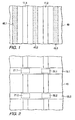
Fig. 1 is plan view of a substrate with columns for the sources and drains. -
Fig. 2 is a plan view of the substrate where word lines with floating gates are formed in rows across the columns. -
Fig. 3 is a further view ofFig. 2 where the sources and the body ties are formed in the columns of the array. -
Fig. 4 is a further view where drains are formed. -
Fig. 5 is a cross suction view taken along the line 5-5' ofFig. 4 and shows the structure of two serially connected floating gate transistors. -
Fig. 6 is a partial electrical schematic of the array. -
Fig. 7 is a cross sectional view taken along the line 7-7' and through source regions in a adjacent columns. -
Fig. 8 is a cross sectional view taken along the line of 8-8' and through drain regions in adjacent columns. -
Figs. 9 -11 show steps for making the deep trenches. -
Figs. 12-19 show stops for making a system on chip devices with memory, logic and linear transistors. - Turning to
Fig. 1 , there is shown a P-type substrate 40. A deep N-well 41 is formed in thesubstrate 40 and a number of high voltage (HV) P-wells 42 are formed in the deep N-well. The surface of thesubstrate 40 is masked with a screen oxide 45 or other suitable mask to form openings 11.1, 11.2, ... 11.n for the columns of the array. The active areas in a column are isolated from adjacent active areas by deep trenches 46.1, 46.2, 46.3, ... 46.n that extend below the deep N-well 41. In order to explain the rest of the structure, the deep trenches are omitted fromFigs. 2 and3 . Progressing toFig. 2 , thesubstrate 40 is further processed to form a plurality of word lines 15.1, 15.2, ... 15.n that extend as rows that cross the columns 11.n. For each transistor a floating gate structure is formed over the crossing of the word line and the column. - Common sources such as 22, 27 and 32, 37 are formed between the word lines. A
P+ body implant line 14. A raised commondrain bit line 13 will be formed later in the process over the buried source bit line so that the source and drain bit lines will be substantially vertically aligned with each other. - The drain regions, such as 23, 28 and 33, 38 are shown in
Fig. 4 . The raiseddrain bit lines 13 are formed frommetal 1 that passes through vias to contact the drains. As shown inFigs. 3, 4 the raisedbit line 13 is connect to the drains and the buriedbit line 14 is connected to the sources. They occupy about the same planar location but are separated vertically from each other. For purposes of illustration, the buriedbit line 14 is shown in dashed outline in both figures and is wider than the raisedbit line 13. In practice, the lines may be the same or different widths. Each combined drain region has a contact 50n that extends to the surface of the device. The contacts 50n are isolated from each other and from the floating gate stack 60.n, 61.n, 62.n, 63.n. The contacts 50n extend vertically through theisolation layer 54 to contact thedrain regions substrate 40, as shown inFigs. 4 ,8 . The contacts are formed by opening vias in the insulation layer, depositing a layer of metal 500 over theinsulation layer 54 and in its vias, and then patterning the metal layer 500 into a set of metal lines 500.1, 500.2, ... 5000.n that form the raised bit lines of the array, one metal line per bit line. - Both of these wells (HV P-wells and deep N-wells) are to be shared in the memory region as well as in the HV peripheral regions to reduce mask costs. The wells are formed with a high energy implant process that is known as the "retrograde well process" in the semiconductor industry. The implant has a depth profile that is typically greater than 0.7µm for P and greater than 1.5µm for N. That profile is necessary in order for the memory to generate sufficient high voltage, typically greater than 12V, to avoid junction punch-through for write and erase operations.
-
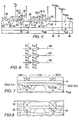
Fig. 5 shows a typical floating gate structure that includes an insulating tunnel oxide layer 63 (typically thin SiO2 or oxynitride) on the surface of thesubstrate 40, a first conductive, charge storage layer on the insulating layer that forms the floating gate 62, an insulating; layer 61 (typically an ONO layer) on the lower conductive layer, and a second conductive layer on the charge storage layer that forms the control gate 60. In response to a set of voltages applied to the control electrodes and to the wells, charge may be stored, or erased from the floating gate transistor or the charging state will be sensed in the read mode. The function and operation of triple well floating gate transistors arc known. Details of their structure, manufacture and operation are provided in one or more of my other patents or pending applications. My patent and pending applications includesU.S. Pat. No. 6,307,781 , andU.S. Serial Nos. 10/234,344 filed September 4, 2002 US 2004/0041205 A1 and10/057,039, filed January 25, 2002 US 2003/0142541 A1 . - Portions of the active areas between deep trenches are masked and self-aligned openings to
spacers Source regions wells 42. The deep trenches prevent the sources from laterally spreading into adjacent columns. The sources are further masked and self-aligned to spacers 91, 92. A P-type implant is made into the opening betweenspacers bit line 14 in the common P-well 42. This buried bit line resistance is further reduced by subsequent silicide process prior to contact formation. Such silicidation must take place in theP + 24 overlap the n- region, extend to both ends of n- region 22 and 27 but avoid extend to under the gate edge. Not every combined source region has a contact by a metal strap. It is sufficient to form contact with an upper level metal strap every thirty-two or sixty-four word lines 15 to reduce well resistance while maintain single metal line per bitline simplicity. The added upper level of metal is simple to add and does not adversely effect the footprint of the embedded memory array because its core processor already uses many level of metals. - The transistors in a typical cell of the array are shown in
Fig. 5 . Thesubstrate 40 has a deep N-well 41 and a shallow P-well 42. The transistors are in the P-well 42. From left to right, there is adrain region 23, a first floating gate stack (60.1, 61.1, 62.1), first andsecond sources second drain 28.Drain contacts substrate 40 to contact a raised metal bit line 500.Source regions bit lines 14 that are vertically aligned with the raised metal bit lines. A higher (upper level) metal line runs in parallel with and above drain bit line 500 and contacts the source buried bit lines 14. The sources, drains and control gates are silicided. Sidewall oxide and spacers isolate the gates from the drains and sources. As shown inFigs. 7 and 8 , the deep trenches 46.1 and 46.2 separate adjacent columns and buriedbit lines 14 from each other. - As a result of the above structure and the process for forming the structure, the invention achieves cell scaling and provides a uniform channel programming architecture that has buried bit lines with source and P-well ties to replace a conventional metal bit line. Likewise the source and the P-well are held at the same potential during programming, erase and read operations. No surface source contact is needed due to the source and P-well and body tie. In the process, the trenches are etched to a depth of between 1 and 3 microns deep. This deep trench process may be used in conjunction with shallow trench isolation processes that are typically found in logic and linear designs. These and other objects in the invention are achieved by using P+ implants and silicide over the sources and after a spacer is provided in order to provide P+ body ties to the N- body sources.
- The deep trench isolation not only reduces the area of the substrate required to isolate one column from the next. The deep trench isolation also isolates the memory arrays from the high voltage devices including the row and column decoders, transfer gates, etc, and further reduces the isolation area between the high voltage devices to less than one micron compared to the shallow trench isolation of several microns for isolating high voltage devices from memory arrays.
- The triple well provides a separate biasing well for programming. The separate biasing well reduces the gate induced drain leakage. As such, a smaller charge pump may be used and the memory device may be operated at lower power. The deep trench isolation creates decoupling capacitors when the trenches fill with doped material and properly insulating from the top surface, whose capacitance values are few order of magnitude higher than conventional well capacitors and consume much less area; suitable for charge pump design and provides a significant area reduction. In the past, when memory devices have been incorporated with high voltage devices, it was conventional to use shallow trench isolation for the memory transistors and the high voltage transistors with large isolation space (e.g. N+/N+, N+/P+, P+/P+). However, high voltage transistors require more spacing than do memory transistors. By using shallow trench isolation for high voltage devices and deep trench isolation for memory devices, the overall device size is reduced, mostly due to isolation space reduction which was enable by the deep trench technology.
- Turning to
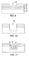
Fig. 9-10 , there are shown the steps involved in fabricating thedeep trench 46. The deep trench is formed at the beginning of the process generally before the shallow trench isolation that is used to separate the high voltage and CMOS devices. This provides a modular approach for System-on-Chip (SoC) and avoids any unwarranted effects introduced by the addition of deep trench process on the base logic process. The following flow is just one embodiment for making devices with the invention. Those skilled in the art will understand that other process steps may be used to achieve equivalent process flow and equivalent devices. As such, the following example is for illustration purpose. The details such as film thickness, deposit temperature, additional films or integration can be varied. - In order to form the deep trench, a
pad oxide layer 70 is deposited on thesubstrate 40. The pad oxide is approximately 53 angstroms thick. Next apad nitride layer 71 with a thickness of 1800 angstroms is deposited over the pad oxide layer. A layer ofBSG 72 is deposited on thepad nitrite layer 71.BSG 72 is patterned by a photoresist mask 73. The mask providesopenings 46 that will ultimately become the deep trenches shown inFig. 9 . First theBSG 72 is removed from the trench followed by resist strip and clean that leaves BSG on active region as a hardmask to protect the substrate from the subsequent deep trench etch. Next is the main Si etch by removal of the nitrite and pad oxide layers and then a portion of thesubstrate material 40 to provide the deep trench structure shown inFig. 10 . Part of theBSG 72 on active region was removed during the deep trench ctch. The remaining BSG over the active region are subsequently removed. Then the trench is filed with a series of four layers. One of the features of this invention is that the trench is formed with a compound dielectric layer on its side walls and bottom. Initially, a layer of Si3N4 75 is deposited using low pressure chemical vapor deposition to form a 4.3 nanometer coating on the walls and floor of the trench. Thereafter, the trench is exposed to dry oxygen and 900 degrees centigrade in order to oxidize portions of the silicon nitrite layer and thereby form a composite dielectric of approximately 5.0 nanometers thickness. The dielectric is further exposed to the rapid thermal nitridation process to convert the top layer into oxynitride (76). Next, using a low pressure chemical vapor deposition process undopedamorphous polysilicon 77 is deposited in the trench. The polysilicon is chemically and mechanically polished to provide a recess of approximately 0.5 microns. The remainder of the trench is filled with a chemical vapor deposition layer of TEOS that is approximately 5000 angstroms thick. TheTEOS 78 is then chemically and mechanically polished. Thereafter; the high voltage, CMOS and memory devices may be formed in accordance with the process steps known in the art or set forth in my co-pendingU.S. Patent Application Serial No. 10/234,334 filed September 4,2002 US 2004/0041205 A1 . The process disclosed in that co-pending application is carried through until just prior to forming the N+ source and drains and P+ source and drains of the CMOS and memory devices. At that point, the process described at the beginning of this specification is inserted in order to form the buried source bit line of the invention. During formation of the buried source bit line of the invention, the rest of the device is masked so that only the sources of the memory array arc formed. Likewise, after completion of formation of the memory array, the memory array is then masked and the CMOS devices are opened in order to form the N+ and P+ sources and drains. - The process described above may be modified still used deep trench isolation formation and add decoupling capacitor. This may be achieved by replacing the
undoped polysilicon 77 with a doped polysilicon in a well known in-situ doped process; e.g. doping is through gas flow during the deposition for better uniformity. Suitable gases such as phosphine (PH3) and B2H6 for N-doped and P-doped polysilicon, respectively, are flowed over the deep Nwells for positive polarity, or over the Pwcll or substrate for negative polarity. For the memory array portion, we follow above flow with the polysilicon chemically and mechanically polished to provide a recess of approximately 0.5 microns. The remainder of the trench is filled with a chemical vapor deposition layer of TEOS that is approximately 5000 angstroms thick. For the decoupling capacitor portion, none or a small recess is provided in the end and the process adds contacts for the top electrode connection. - Turning to
Figure 12 , the P-type substrate 40 is suitably patterned to form shallowtrench isolation regions 120. Thetrench isolation regions 120 each pair of CMOS transistors and any linear or high voltage devices formed on the substrate. Thedeep trenches 46 separate the memory columns from each other and from the other devices. Those skilled in the art understand that the invention may be made on an N-type substrate where the dopings are suitable reversed. As shown inFigure 13 , the substrate is then covered with a floatinggate oxide 121 followed by alayer 122 of polysilicon. Prior to deposition of the layers, a suitable portion of the substrate, such as portion A, is separately patterned and implanted to have a triple-well comprising N-well 41 that encloses P-well 42. A logic CMOS pair of transistors are in region B. Those B regions may include transistors other than CMOS logic pairs. Those skilled in the art understand that transistor of one conductivity type may be formed in the B regions and types of transistors may be logic or linear, including and not limited to power transistors such as LDMOS transistors. - The oxide and polysilicon layers are then patterned with
photoresist 123 to form a floating gate slot (parallel to bitline). Turning toFig. 14 , alayer 124 of ONO interpoly dielectric is deposited over the substrate. Thelayer 124 comprises sequentially a thermally grown bottom oxide, a deposited layer of low temperature deposited polysilicon that is reoxidized to form top oxide at later time. Thelayer 124 is suitably patterned byphotoresist 123 to form two of the three layers of the ONO interpoly dielectric in the EEPROM stack as shown inFig. 15 . At this point, thelayer 124 and polysilicon layer 111 are stripped from the peripheral regions B and they are suitably patterned and implanted to form P-wells 142 and N-wells 141. - As shown in
Fig. 16 , thesubstrate 40 is covered with alayer 125 of oxide followed by asecond layer ofpolysilicon 126. Thelayer 125 forms the gate oxide layer for the logic and linear devices and forms the upper oxide layer of theONO dielectric layer 124. Thepolysilicon layer 126 is patterned and etched to form the control gates of the EEPROM transistors and the logic and linear transistors. - The description below creates a dual sidewall oxide that optimizes a memory cell's reliability and maintains a shallow logic device S/D junction, similar to my copending
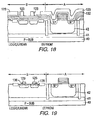
US Patent Application Serial Number 10/234,344, filed September 4, 2002 US 2004/0041205 A1 . Afirst TEOS layer 130 is deposited over thesecond polysilicon layer 126. Thefirst TEOS layer 130 is then suitably patterned withphotoresist 123 to open the source and drain regions of the EEPROM. Source and drain regions are suitably implanted to form the source and drains of the EEPROM. (SeeFig. 17 ) After that, thefirst TEOS layer 130 is removed by a high selective reactive ion etching, stopping onpolysilicon layer 126. Then the sidewalls of the gate stack of the EEPROM are oxidized to provide a sidewall oxide suitable for flash stack transistors. Oxidation takes place at about 850-950° centigrade in a furnace for approximately 30 minutes in order to grow a sidewall that is about 15 nanometers thick on the polysilicon regions of the gate stack. (SeeFig. 18 ) Thereafter, asecond TEOS layer 132 is deposited over thesubstrate 40.TEOS layer 132 is suitably patterned with aphotoresist layer 123 to form the gates and to open the source and drains of the logic and linear transistors. (SeeFig. 19 ) - The sources and drains of the logic and/or linear transistors are implanted, the
second TEOS layer 132 is removed by reactive ion etching and the gates of the peripheral transistors receive a thinner sidewall oxide. That sidewall oxide is approximately 6 nanometers and is generated by a relatively short rapid thermal annealing step. The rapid thermal annealing is carried out at about 700-900°C for about 10-20 second. It activates the doping in the logic and/or linear transistors but does not drive them very far into the substrate. This results in a logic and/or linear region with relatively closely spaced transistors. - Then the substrate is masked to expose only selected source regions in the memory array. Those regions are exposed and implanted with a P-type implant to form the P+ body ties, to the source N- junctions of the memory. Additional metal straps from upper levels of metal (e.g. M3) will bring the source rail resistance down. Not every source regions requires a metal strap and every thirty-second or sixty-fourth source region is sufficient. No bitline pitch increase due to the addition of metal strap M3 since both M1 bitline and M3 source line run on top of each other. Those skilled in the art can realize the benefit and achieve a 50% cell area reduction or ~30% chip reduction.
- As a result of the process described above a manufacturer may produce a single integrated circuit with logic and/or linear and memory devices having different sidewall insulating thicknesses. In the logic and/or linear region the sidewalls can be optimized to be as thin as needed to provide more transistor in the region allowed for logic and/or linear devices. In the memory region the memory devices are optimized to have a thick enough sidewall oxide to prevent the charge stored in the interpoly dielectric layer from having an unwanted effect on the operation of the memory transistors.
- The triple well allows the user to control the voltage on the deep buried N-well 41 and the shallow P-well 42 in order to program, erase and read the array. A typical set of operating parameters to program, erase and read appears in the following table where the voltages applied to the selected and unselected components are identified.
TABLE 1 Read (volts) Program (volts) Erase (volts) Selected Cells Gate VPP = 2.5 +14 volts -14 Drain) VDD = 1.2 -3 +3 Source/P-Well 0 -3 +3 Deep N-Well 0 0 +3 Unselected Cells Gate 0 0/-3 0/+3 Drain disturb DR turn-on Drain 0 +3 +3 Grate disturb R. disturb Source/P-well 0 +3 +3 Deep N-well 0 +3 +3 - In operation, when the user desires to read the contents of a given transistor cell, the word line associated with the transistor is raised to approximately 2.5 volts. Likewise, the bit line connected to the drain is coupled to a voltage of approximately 1.25 volts. The output of the cell then appears on the other or source bit line. The deep N well is held at zero volts. The voltages for all of the other electrodes of the rest of the array are set to zero volts.
- In order to program a transistor, the word line of the gate with the selected transistor are raised to +14 volts. The drain bit line is lowered to -3 volts as is the buried source bit line to provide a uniform voltage across the channel. The deep N well 41 is set to zero volts. The gates of the unselected transistors are either set to zero or -3 volts and the other electrodes are set to +3 volts. In order to erase a program transistor, the drain and the source bit lines are set to +3 volts and the gate is set to -14 volts. The gates of the unselected transistors are set to between zero and +3 volts and all of the other electrodes are set to +3 volts.
- The configuration of the array is shown schematically in
Fig. 6 . The drain and source regions arc aligned with each other in a given column and the columns 11.n are parallel to each other. The word lines 15.n run transverse to the columns 11.n. The drains are connected together by a first, raisedbit line 13. The sources are connected together by a buriedbit line 14. With this arrangement, there source and drain regions arc aligned with each other and require minimal active areas. Likewise, there is only one metal line. This reduces the complexity of interconnnecting the transistors and save valuable space in the active areas of the device. With the invention only one set of vias and vertical contacts are needed for the single metal line.
Claims (7)
- A semiconductor device with an array of flash memory cells comprising:a semiconductor substrate;a repeated cell arranged in columns and rows and comprising transistors with floating gates;in each cell a common source (22,27) for adjacent transistors;first and second floating gates (62) on opposite sides of the common source;first and second drains (23, 28), respectively, on the other side of the first and second floating gates;wherein the common sources are connected together in a buried bit line (14) in the substrate and the drains are aligned with each other and connected to a metal contact layer disposed over the substrate and aligned with the drains and source,wherein each common source has a body tie (24,34) of opposite polarity to the source polarity and of a silicide overlapping a region of the opposite polarity, characterised in that
the silicided regions of the body ties are self-aligned to spacers (91, 92) on the gates of the transistors. - The device of claim 1 further comprising a deep trench (46) disposed between adjacent columns for isolating the transistors in each column from the transistors in the adjacent columns.
- The device of claim 2 having a substrate of a first polarity, a deep well of a second and opposite polarity, wherein the deep trench extends to or beyond the depth of the deep well of the second polarity.
- A process for fabricating a system on chip device in a semiconductor substrate, the device having low power logic devices, higher power driver devices and a flash memory array comprising a plurality of floating gate transistors, said floating gate transistors arranged with their sources and drains aligned in columns;
forming a plurality of word lines extending transverse to the columns to form a plurality of rows, with each word line connected to the floating gates of the transistors beneath the word line;
forming columns comprising a plurality of first and second floating gate transistors wherein each first and second floating gate transistor has a drain (23, 28), a source (22, 27) and floating gate (62) between its drain and source;
in each column forming common source regions disposed between opposite sides of the first and second floating gates to provide the sources for two adjacent transistors;
in each column forming first and second drain regions disposed respectively on the other sides of the first and second floating gates;
in each column forming drain contacts aligned with the sources for contacting the first and second drains of the first and second floating gate transistors in each column;
in each column forming a first bit lines (14) buried beneath the surface of the substrate for connecting together the common sources of the floating gate transistors;
in each column forming a second raised bit line (13) disposed over the substrate and over the buried bit line and having contacts extending to the surface to contact the drains on floating gate transistors in the column; and
forming a deep trench (46) disposed between adjacent columns for isolating the transistors in each column from the transistors in the adjacent columns,
implanting body tie dopants self aligned to spacers (91, 92) into the source regions to form body ties (24, 34) and siliciding the body ties with overlap to the body tie dopants and extending to both ends of the source regions but avoiding extend to under the gate edge. - The process of claim 4 wherein the body tie implants have a polarity opposite to the polarity of the source regions.
- The process of claim 4 comprising:forming first wells of a polarity opposite the polarity of the sources and drains;forming seconds wells surrounding the first wells and of a polarity the same as the sources and drains;forming third wells of a polarity the same as the first well;forming the deep trenches deep enough to penetrate the second wells.
- The process of claim 4 wherein the third wells comprises the substrate.
Applications Claiming Priority (2)
| Application Number | Priority Date | Filing Date | Title |
|---|---|---|---|
| US10/607,610 US6909139B2 (en) | 2003-06-27 | 2003-06-27 | One transistor flash memory cell |
| PCT/EP2004/051254 WO2005001937A2 (en) | 2003-06-27 | 2004-06-25 | One transistor flash memory cell |
Publications (2)
| Publication Number | Publication Date |
|---|---|
| EP1639638A2 EP1639638A2 (en) | 2006-03-29 |
| EP1639638B1 true EP1639638B1 (en) | 2011-05-11 |
Family
ID=33540312
Family Applications (1)
| Application Number | Title | Priority Date | Filing Date |
|---|---|---|---|
| EP04741900A Expired - Lifetime EP1639638B1 (en) | 2003-06-27 | 2004-06-25 | Flash memory cell array |
Country Status (5)
| Country | Link |
|---|---|
| US (2) | US6909139B2 (en) |
| EP (1) | EP1639638B1 (en) |
| KR (1) | KR100760755B1 (en) |
| DE (2) | DE112004001244B4 (en) |
| WO (1) | WO2005001937A2 (en) |
Cited By (1)
| Publication number | Priority date | Publication date | Assignee | Title |
|---|---|---|---|---|
| CN102386101A (en) * | 2010-08-20 | 2012-03-21 | 长城半导体公司 | Semiconductor device and method of forming low voltage MOSFET for portable electronic devices and data processing centers |
Families Citing this family (44)
| Publication number | Priority date | Publication date | Assignee | Title |
|---|---|---|---|---|
| US6909139B2 (en) * | 2003-06-27 | 2005-06-21 | Infineon Technologies Ag | One transistor flash memory cell |
| US7119393B1 (en) * | 2003-07-28 | 2006-10-10 | Actel Corporation | Transistor having fully-depleted junctions to reduce capacitance and increase radiation immunity in an integrated circuit |
| TW589708B (en) * | 2003-08-19 | 2004-06-01 | Nanya Technology Corp | Method for defining deep trench in substrate and multi-layer hard mask structure for defining the same |
| US7122437B2 (en) * | 2003-12-19 | 2006-10-17 | Infineon Technologies Ag | Deep trench capacitor with buried plate electrode and isolation collar |
| KR100642930B1 (en) * | 2003-12-27 | 2006-11-03 | 동부일렉트로닉스 주식회사 | Embedded nonvolatile memory device with high integration and manufacturing method |
| US7023740B1 (en) * | 2004-01-12 | 2006-04-04 | Advanced Micro Devices, Inc. | Substrate bias for programming non-volatile memory |
| US7365385B2 (en) * | 2004-08-30 | 2008-04-29 | Micron Technology, Inc. | DRAM layout with vertical FETs and method of formation |
| US7679130B2 (en) * | 2005-05-10 | 2010-03-16 | Infineon Technologies Ag | Deep trench isolation structures and methods of formation thereof |
| US7285818B2 (en) * | 2005-06-15 | 2007-10-23 | Actel Corporation | Non-volatile two-transistor programmable logic cell and array layout |
| US7538379B1 (en) | 2005-06-15 | 2009-05-26 | Actel Corporation | Non-volatile two-transistor programmable logic cell and array layout |
| US7495279B2 (en) * | 2005-09-09 | 2009-02-24 | Infineon Technologies Ag | Embedded flash memory devices on SOI substrates and methods of manufacture thereof |
| US20070133289A1 (en) * | 2005-12-01 | 2007-06-14 | Aplus Flash Technology, Inc. | NAND-type flash memory device with high voltage PMOS and embedded poly and methods of fabricating the same |
| US7679125B2 (en) * | 2005-12-14 | 2010-03-16 | Freescale Semiconductor, Inc. | Back-gated semiconductor device with a storage layer and methods for forming thereof |
| KR100760634B1 (en) * | 2006-10-02 | 2007-09-20 | 삼성전자주식회사 | NAND type nonvolatile memory device and method of forming the same |
| US20080112231A1 (en) * | 2006-11-09 | 2008-05-15 | Danny Pak-Chum Shum | Semiconductor devices and methods of manufacture thereof |
| JP2009206492A (en) * | 2008-01-31 | 2009-09-10 | Toshiba Corp | Semiconductor device |
| US20110042722A1 (en) * | 2009-08-21 | 2011-02-24 | Nanya Technology Corp. | Integrated circuit structure and memory array |
| US8455923B2 (en) | 2010-07-01 | 2013-06-04 | Aplus Flash Technology, Inc. | Embedded NOR flash memory process with NAND cell and true logic compatible low voltage device |
| KR20120010642A (en) * | 2010-07-22 | 2012-02-06 | 삼성전자주식회사 | Nonvolatile Memory Device, Manufacturing Method and Driving Method thereof |
| US8399310B2 (en) | 2010-10-29 | 2013-03-19 | Freescale Semiconductor, Inc. | Non-volatile memory and logic circuit process integration |
| US9093266B2 (en) * | 2011-04-11 | 2015-07-28 | Micron Technology, Inc. | Forming high aspect ratio isolation structures |
| US8906764B2 (en) | 2012-01-04 | 2014-12-09 | Freescale Semiconductor, Inc. | Non-volatile memory (NVM) and logic integration |
| US8951863B2 (en) | 2012-04-06 | 2015-02-10 | Freescale Semiconductor, Inc. | Non-volatile memory (NVM) and logic integration |
| US9087913B2 (en) | 2012-04-09 | 2015-07-21 | Freescale Semiconductor, Inc. | Integration technique using thermal oxide select gate dielectric for select gate and apartial replacement gate for logic |
| US9111865B2 (en) | 2012-10-26 | 2015-08-18 | Freescale Semiconductor, Inc. | Method of making a logic transistor and a non-volatile memory (NVM) cell |
| US9006093B2 (en) | 2013-06-27 | 2015-04-14 | Freescale Semiconductor, Inc. | Non-volatile memory (NVM) and high voltage transistor integration |
| US8871598B1 (en) | 2013-07-31 | 2014-10-28 | Freescale Semiconductor, Inc. | Non-volatile memory (NVM) and high-k and metal gate integration using gate-first methodology |
| US9129996B2 (en) | 2013-07-31 | 2015-09-08 | Freescale Semiconductor, Inc. | Non-volatile memory (NVM) cell and high-K and metal gate transistor integration |
| US8877585B1 (en) * | 2013-08-16 | 2014-11-04 | Freescale Semiconductor, Inc. | Non-volatile memory (NVM) cell, high voltage transistor, and high-K and metal gate transistor integration |
| US9082837B2 (en) | 2013-08-08 | 2015-07-14 | Freescale Semiconductor, Inc. | Nonvolatile memory bitcell with inlaid high k metal select gate |
| US9082650B2 (en) | 2013-08-21 | 2015-07-14 | Freescale Semiconductor, Inc. | Integrated split gate non-volatile memory cell and logic structure |
| US9252246B2 (en) | 2013-08-21 | 2016-02-02 | Freescale Semiconductor, Inc. | Integrated split gate non-volatile memory cell and logic device |
| US9275864B2 (en) | 2013-08-22 | 2016-03-01 | Freescale Semiconductor,Inc. | Method to form a polysilicon nanocrystal thin film storage bitcell within a high k metal gate platform technology using a gate last process to form transistor gates |
| US8932925B1 (en) | 2013-08-22 | 2015-01-13 | Freescale Semiconductor, Inc. | Split-gate non-volatile memory (NVM) cell and device structure integration |
| US9136129B2 (en) | 2013-09-30 | 2015-09-15 | Freescale Semiconductor, Inc. | Non-volatile memory (NVM) and high-k and metal gate integration using gate-last methodology |
| US9129855B2 (en) | 2013-09-30 | 2015-09-08 | Freescale Semiconductor, Inc. | Non-volatile memory (NVM) and high-k and metal gate integration using gate-first methodology |
| US8901632B1 (en) | 2013-09-30 | 2014-12-02 | Freescale Semiconductor, Inc. | Non-volatile memory (NVM) and high-K and metal gate integration using gate-last methodology |
| US9231077B2 (en) | 2014-03-03 | 2016-01-05 | Freescale Semiconductor, Inc. | Method of making a logic transistor and non-volatile memory (NVM) cell |
| US9112056B1 (en) | 2014-03-28 | 2015-08-18 | Freescale Semiconductor, Inc. | Method for forming a split-gate device |
| US9472418B2 (en) | 2014-03-28 | 2016-10-18 | Freescale Semiconductor, Inc. | Method for forming a split-gate device |
| US9379222B2 (en) | 2014-05-30 | 2016-06-28 | Freescale Semiconductor, Inc. | Method of making a split gate non-volatile memory (NVM) cell |
| US9257445B2 (en) | 2014-05-30 | 2016-02-09 | Freescale Semiconductor, Inc. | Method of making a split gate non-volatile memory (NVM) cell and a logic transistor |
| US9343314B2 (en) | 2014-05-30 | 2016-05-17 | Freescale Semiconductor, Inc. | Split gate nanocrystal memory integration |
| KR102457732B1 (en) * | 2017-12-28 | 2022-10-21 | 선라이즈 메모리 코포레이션 | Three-dimensional NOR memory array with ultra-fine pitch: apparatus and method |
Family Cites Families (45)
| Publication number | Priority date | Publication date | Assignee | Title |
|---|---|---|---|---|
| US635415A (en) * | 1899-01-26 | 1899-10-24 | James Henry Plummer | Drill. |
| US4979004A (en) * | 1988-01-29 | 1990-12-18 | Texas Instruments Incorporated | Floating gate memory cell and device |
| JP2806552B2 (en) | 1989-05-25 | 1998-09-30 | 日本電気株式会社 | Semiconductor nonvolatile storage device |
| JPH04164372A (en) | 1990-10-29 | 1992-06-10 | Toshiba Corp | Semiconductor integrated circuit |
| US5315142A (en) | 1992-03-23 | 1994-05-24 | International Business Machines Corporation | High performance trench EEPROM cell |
| US5412238A (en) * | 1992-09-08 | 1995-05-02 | National Semiconductor Corporation | Source-coupling, split-gate, virtual ground flash EEPROM array |
| US5429970A (en) * | 1994-07-18 | 1995-07-04 | United Microelectronics Corporation | Method of making flash EEPROM memory cell |
| US5635415A (en) * | 1994-11-30 | 1997-06-03 | United Microelectronics Corporation | Method of manufacturing buried bit line flash EEPROM memory cell |
| US5644632A (en) * | 1995-06-07 | 1997-07-01 | Lucent Technologies Inc. | Distributed key telephone station network |
| TW347567B (en) | 1996-03-22 | 1998-12-11 | Philips Eloctronics N V | Semiconductor device and method of manufacturing a semiconductor device |
| TW382147B (en) * | 1996-05-31 | 2000-02-11 | United Microeletronics Corp | Trench-type condensed junction-less flash memory and manufacturing method thereof |
| JPH1117035A (en) * | 1997-06-24 | 1999-01-22 | Mitsubishi Electric Corp | Nonvolatile semiconductor memory device and method of manufacturing the same |
| FR2767219B1 (en) * | 1997-08-08 | 1999-09-17 | Commissariat Energie Atomique | ELECTRICALLY COMPATIBLE PROGRAMMABLE AND ERASABLE NON-VOLATILE MEMORY DEVICE WITH A CMOS / SELF-MANUFACTURING PROCESS |
| DE59914434D1 (en) * | 1998-02-27 | 2007-09-13 | Qimonda Ag | METHOD FOR PRODUCING AN ELECTRICALLY PROGRAMMABLE MEMORY CELL ARRANGEMENT |
| US6327182B1 (en) * | 1998-06-22 | 2001-12-04 | Motorola Inc. | Semiconductor device and a method of operation the same |
| DE19932590A1 (en) * | 1999-07-13 | 2001-01-18 | Lissotschenko Vitalij | Device for generating lines or line groups of electromagnetic radiation in the optical spectral range |
| US6628544B2 (en) * | 1999-09-30 | 2003-09-30 | Infineon Technologies Ag | Flash memory cell and method to achieve multiple bits per cell |
| US6307781B1 (en) * | 1999-09-30 | 2001-10-23 | Infineon Technologies Aktiengesellschaft | Two transistor flash memory cell |
| US6198658B1 (en) * | 1999-10-08 | 2001-03-06 | Hyundai Electronics America, Inc. | High density flash memory architecture with columnar substrate coding |
| TW441038B (en) * | 2000-01-10 | 2001-06-16 | United Microelectronics Corp | Manufacturing method of ETOX flash memory |
| TW448576B (en) * | 2000-03-21 | 2001-08-01 | United Microelectronics Corp | V-shape flash memory and its manufacturing |
| US6438030B1 (en) | 2000-08-15 | 2002-08-20 | Motorola, Inc. | Non-volatile memory, method of manufacture, and method of programming |
| KR100350810B1 (en) * | 2000-09-21 | 2002-09-05 | 삼성전자 주식회사 | Shallow trench isolation type semiconductor device and method of forming the same |
| US6626644B2 (en) * | 2000-10-30 | 2003-09-30 | Ntn Corporation | Magnetically levitated pump and controlling circuit |
| JP4008651B2 (en) * | 2000-10-31 | 2007-11-14 | 株式会社東芝 | Semiconductor device and manufacturing method thereof |
| US6436845B1 (en) * | 2000-11-28 | 2002-08-20 | Lsi Logic Corporation | Silicon nitride and silicon dioxide gate insulator transistors and method of forming same in a hybrid integrated circuit |
| US6667226B2 (en) * | 2000-12-22 | 2003-12-23 | Texas Instruments Incorporated | Method and system for integrating shallow trench and deep trench isolation structures in a semiconductor device |
| US6600199B2 (en) * | 2000-12-29 | 2003-07-29 | International Business Machines Corporation | Deep trench-buried layer array and integrated device structures for noise isolation and latch up immunity |
| JP2002237575A (en) * | 2001-02-08 | 2002-08-23 | Sharp Corp | Semiconductor device and manufacturing method thereof |
| US6436751B1 (en) * | 2001-02-13 | 2002-08-20 | United Microelectronics Corp. | Fabrication method and structure of a flash memory |
| KR100381953B1 (en) * | 2001-03-16 | 2003-04-26 | 삼성전자주식회사 | Method of fabricating nor type flash memory device |
| JP2003007864A (en) * | 2001-06-22 | 2003-01-10 | Nec Corp | Manufacturing method of nonvolatile semiconductor memory device |
| KR100390918B1 (en) * | 2001-08-30 | 2003-07-12 | 주식회사 하이닉스반도체 | a method for manufacturing of semiconductor memory device |
| US6559008B2 (en) * | 2001-10-04 | 2003-05-06 | Hynix Semiconductor America, Inc. | Non-volatile memory cells with selectively formed floating gate |
| JP4390412B2 (en) * | 2001-10-11 | 2009-12-24 | Necエレクトロニクス株式会社 | Semiconductor device and manufacturing method thereof |
| US6693830B1 (en) * | 2001-10-22 | 2004-02-17 | Lattice Semiconductor Corp. | Single-poly two-transistor EEPROM cell with differentially doped floating gate |
| US20030080366A1 (en) * | 2001-10-29 | 2003-05-01 | Matsushita Electric Industrial Co., Ltd. | Non-volatile semiconductor memory device and manufacturing method thereof |
| US6844588B2 (en) * | 2001-12-19 | 2005-01-18 | Freescale Semiconductor, Inc. | Non-volatile memory |
| US6418060B1 (en) * | 2002-01-03 | 2002-07-09 | Ememory Technology Inc. | Method of programming and erasing non-volatile memory cells |
| US6885080B2 (en) * | 2002-02-22 | 2005-04-26 | International Business Machines Corporation | Deep trench isolation of embedded DRAM for improved latch-up immunity |
| US6864530B2 (en) * | 2002-03-05 | 2005-03-08 | Hynix Semiconductor America, Inc. | High density flash memory architecture with columnar substrate coding |
| US6841824B2 (en) * | 2002-09-04 | 2005-01-11 | Infineon Technologies Ag | Flash memory cell and the method of making separate sidewall oxidation |
| DE10306318B4 (en) * | 2003-02-14 | 2010-07-22 | Infineon Technologies Ag | Semiconductor circuit with trench isolation and manufacturing process |
| US6909139B2 (en) * | 2003-06-27 | 2005-06-21 | Infineon Technologies Ag | One transistor flash memory cell |
| US6864151B2 (en) * | 2003-07-09 | 2005-03-08 | Infineon Technologies Ag | Method of forming shallow trench isolation using deep trench isolation |
-
2003
- 2003-06-27 US US10/607,610 patent/US6909139B2/en not_active Expired - Fee Related
-
2004
- 2004-06-25 DE DE112004001244T patent/DE112004001244B4/en not_active Expired - Fee Related
- 2004-06-25 EP EP04741900A patent/EP1639638B1/en not_active Expired - Lifetime
- 2004-06-25 WO PCT/EP2004/051254 patent/WO2005001937A2/en not_active Ceased
- 2004-06-25 DE DE112004003060.9T patent/DE112004003060B4/en not_active Expired - Fee Related
- 2004-06-25 KR KR1020057025110A patent/KR100760755B1/en not_active Expired - Fee Related
-
2005
- 2005-03-16 US US11/081,886 patent/US7190022B2/en not_active Expired - Fee Related
Cited By (1)
| Publication number | Priority date | Publication date | Assignee | Title |
|---|---|---|---|---|
| CN102386101A (en) * | 2010-08-20 | 2012-03-21 | 长城半导体公司 | Semiconductor device and method of forming low voltage MOSFET for portable electronic devices and data processing centers |
Also Published As
| Publication number | Publication date |
|---|---|
| US6909139B2 (en) | 2005-06-21 |
| DE112004001244B4 (en) | 2009-02-05 |
| US7190022B2 (en) | 2007-03-13 |
| US20050180215A1 (en) | 2005-08-18 |
| WO2005001937A2 (en) | 2005-01-06 |
| DE112004003060B4 (en) | 2015-09-03 |
| US20040262669A1 (en) | 2004-12-30 |
| KR20060029153A (en) | 2006-04-04 |
| DE112004001244T5 (en) | 2006-06-01 |
| WO2005001937A3 (en) | 2005-04-07 |
| KR100760755B1 (en) | 2007-09-21 |
| EP1639638A2 (en) | 2006-03-29 |
Similar Documents
| Publication | Publication Date | Title |
|---|---|---|
| EP1639638B1 (en) | Flash memory cell array | |
| US8258028B2 (en) | Deep trench isolation structures and methods of formation thereof | |
| US8031532B2 (en) | Methods of operating embedded flash memory devices | |
| US6177703B1 (en) | Method and apparatus for producing a single polysilicon flash EEPROM having a select transistor and a floating gate transistor | |
| CN1327526C (en) | Programming Method of Electrically Erasable Programmable Read-Only Memory Array | |
| US8344443B2 (en) | Single poly NVM devices and arrays | |
| US7119406B2 (en) | Semiconductor integrated circuit device having deposited layer for gate insulation | |
| US8400828B2 (en) | Nonvolatile semiconductor memory device | |
| JP4463954B2 (en) | Nonvolatile memory device having bulk bias contact structure in cell array region | |
| US6809385B2 (en) | Semiconductor integrated circuit device including nonvolatile semiconductor memory devices having control gates connected to common contact section | |
| US6143607A (en) | Method for forming flash memory of ETOX-cell programmed by band-to-band tunneling induced substrate hot electron and read by gate induced drain leakage current | |
| CN1316625C (en) | Non-volatile memory and its manufacturing method | |
| US20050287741A1 (en) | Nonvolatile memory fabrication methods in which a dielectric layer underlying a floating gate layer is spaced from an edge of an isolation trench and/or an edge of the floating gate layer | |
| US7163863B2 (en) | Vertical memory cell and manufacturing method thereof | |
| US20060214254A1 (en) | Semiconductor device and manufacturing method of the same | |
| US20090021986A1 (en) | Operating method of non-volatile memory device | |
| US6741501B2 (en) | Nonvolatile semiconductor memory device and manufacturing method thereof | |
| US20050275002A1 (en) | Vertical split gate memory cell and manufacturing method thereof | |
| CN100533740C (en) | Integrated circuit including non-volatile memory | |
| US8236679B2 (en) | Manufacturing method of semiconductor memory device using insulating film as charge storage layer | |
| US20080112231A1 (en) | Semiconductor devices and methods of manufacture thereof | |
| US5592002A (en) | Non-volatile semiconductor memory device having reduced current consumption | |
| US6846712B2 (en) | Fabrication of gate dielectric in nonvolatile memories having select, floating and control gates | |
| JP3947041B2 (en) | Semiconductor device and manufacturing method thereof | |
| US7186612B2 (en) | Non-volatile DRAM and a method of making thereof |
Legal Events
| Date | Code | Title | Description |
|---|---|---|---|
| PUAI | Public reference made under article 153(3) epc to a published international application that has entered the european phase |
Free format text: ORIGINAL CODE: 0009012 |
|
| 17P | Request for examination filed |
Effective date: 20051121 |
|
| AK | Designated contracting states |
Kind code of ref document: A2 Designated state(s): FR IT |
|
| DAX | Request for extension of the european patent (deleted) | ||
| RBV | Designated contracting states (corrected) |
Designated state(s): FR IT |
|
| RIN1 | Information on inventor provided before grant (corrected) |
Inventor name: KAKOSCHKE, RONALD Inventor name: TEMPEL, GEORG Inventor name: SHUM, DANNY |
|
| RAP1 | Party data changed (applicant data changed or rights of an application transferred) |
Owner name: INFINEON TECHNOLOGIES AG |
|
| 17Q | First examination report despatched |
Effective date: 20100608 |
|
| GRAP | Despatch of communication of intention to grant a patent |
Free format text: ORIGINAL CODE: EPIDOSNIGR1 |
|
| RTI1 | Title (correction) |
Free format text: FLASH MEMORY CELL ARRAY |
|
| GRAS | Grant fee paid |
Free format text: ORIGINAL CODE: EPIDOSNIGR3 |
|
| GRAA | (expected) grant |
Free format text: ORIGINAL CODE: 0009210 |
|
| AK | Designated contracting states |
Kind code of ref document: B1 Designated state(s): FR IT |
|
| PLBE | No opposition filed within time limit |
Free format text: ORIGINAL CODE: 0009261 |
|
| STAA | Information on the status of an ep patent application or granted ep patent |
Free format text: STATUS: NO OPPOSITION FILED WITHIN TIME LIMIT |
|
| 26N | No opposition filed |
Effective date: 20120214 |
|
| REG | Reference to a national code |
Ref country code: FR Ref legal event code: PLFP Year of fee payment: 12 |
|
| PGFP | Annual fee paid to national office [announced via postgrant information from national office to epo] |
Ref country code: IT Payment date: 20150622 Year of fee payment: 12 Ref country code: FR Payment date: 20150619 Year of fee payment: 12 |
|
| REG | Reference to a national code |
Ref country code: FR Ref legal event code: ST Effective date: 20170228 |
|
| PG25 | Lapsed in a contracting state [announced via postgrant information from national office to epo] |
Ref country code: FR Free format text: LAPSE BECAUSE OF NON-PAYMENT OF DUE FEES Effective date: 20160630 |
|
| PG25 | Lapsed in a contracting state [announced via postgrant information from national office to epo] |
Ref country code: IT Free format text: LAPSE BECAUSE OF NON-PAYMENT OF DUE FEES Effective date: 20160625 |