EP1635470A1 - Method and apparatus for a CMOS image sensor comprising a distributed amplifier and a multiplexed analog to digital converter - Google Patents
Method and apparatus for a CMOS image sensor comprising a distributed amplifier and a multiplexed analog to digital converter Download PDFInfo
- Publication number
- EP1635470A1 EP1635470A1 EP04255476A EP04255476A EP1635470A1 EP 1635470 A1 EP1635470 A1 EP 1635470A1 EP 04255476 A EP04255476 A EP 04255476A EP 04255476 A EP04255476 A EP 04255476A EP 1635470 A1 EP1635470 A1 EP 1635470A1
- Authority
- EP
- European Patent Office
- Prior art keywords
- input
- image sensor
- amplifier
- output
- pixel
- Prior art date
- Legal status (The legal status is an assumption and is not a legal conclusion. Google has not performed a legal analysis and makes no representation as to the accuracy of the status listed.)
- Ceased
Links
- 238000000034 method Methods 0.000 title claims description 18
- 238000005070 sampling Methods 0.000 claims abstract description 15
- 239000003990 capacitor Substances 0.000 claims description 19
- 238000006243 chemical reaction Methods 0.000 claims description 17
- 230000008878 coupling Effects 0.000 claims description 10
- 238000010168 coupling process Methods 0.000 claims description 10
- 238000005859 coupling reaction Methods 0.000 claims description 10
- 239000007787 solid Substances 0.000 claims description 5
- 238000004891 communication Methods 0.000 claims description 4
- 230000003287 optical effect Effects 0.000 claims description 3
- 238000009792 diffusion process Methods 0.000 description 6
- 230000006872 improvement Effects 0.000 description 2
- 230000009467 reduction Effects 0.000 description 2
- 230000003321 amplification Effects 0.000 description 1
- 230000002238 attenuated effect Effects 0.000 description 1
- 230000008901 benefit Effects 0.000 description 1
- 230000008859 change Effects 0.000 description 1
- 230000000694 effects Effects 0.000 description 1
- 230000008030 elimination Effects 0.000 description 1
- 238000003379 elimination reaction Methods 0.000 description 1
- 230000006870 function Effects 0.000 description 1
- 238000003384 imaging method Methods 0.000 description 1
- 238000002347 injection Methods 0.000 description 1
- 239000007924 injection Substances 0.000 description 1
- 239000002184 metal Substances 0.000 description 1
- 230000004048 modification Effects 0.000 description 1
- 238000012986 modification Methods 0.000 description 1
- 238000003199 nucleic acid amplification method Methods 0.000 description 1
- 230000008569 process Effects 0.000 description 1
- 230000004044 response Effects 0.000 description 1
- 230000000630 rising effect Effects 0.000 description 1
- 239000000758 substrate Substances 0.000 description 1
- 230000007704 transition Effects 0.000 description 1
Images



Classifications
-
- H—ELECTRICITY
- H03—ELECTRONIC CIRCUITRY
- H03M—CODING; DECODING; CODE CONVERSION IN GENERAL
- H03M1/00—Analogue/digital conversion; Digital/analogue conversion
- H03M1/10—Calibration or testing
- H03M1/1009—Calibration
- H03M1/1014—Calibration at one point of the transfer characteristic, i.e. by adjusting a single reference value, e.g. bias or gain error
- H03M1/1023—Offset correction
-
- H—ELECTRICITY
- H04—ELECTRIC COMMUNICATION TECHNIQUE
- H04N—PICTORIAL COMMUNICATION, e.g. TELEVISION
- H04N25/00—Circuitry of solid-state image sensors [SSIS]; Control thereof
- H04N25/60—Noise processing, e.g. detecting, correcting, reducing or removing noise
- H04N25/616—Noise processing, e.g. detecting, correcting, reducing or removing noise involving a correlated sampling function, e.g. correlated double sampling [CDS] or triple sampling
-
- H—ELECTRICITY
- H04—ELECTRIC COMMUNICATION TECHNIQUE
- H04N—PICTORIAL COMMUNICATION, e.g. TELEVISION
- H04N25/00—Circuitry of solid-state image sensors [SSIS]; Control thereof
- H04N25/60—Noise processing, e.g. detecting, correcting, reducing or removing noise
- H04N25/67—Noise processing, e.g. detecting, correcting, reducing or removing noise applied to fixed-pattern noise, e.g. non-uniformity of response
- H04N25/671—Noise processing, e.g. detecting, correcting, reducing or removing noise applied to fixed-pattern noise, e.g. non-uniformity of response for non-uniformity detection or correction
-
- H—ELECTRICITY
- H04—ELECTRIC COMMUNICATION TECHNIQUE
- H04N—PICTORIAL COMMUNICATION, e.g. TELEVISION
- H04N25/00—Circuitry of solid-state image sensors [SSIS]; Control thereof
- H04N25/70—SSIS architectures; Circuits associated therewith
- H04N25/76—Addressed sensors, e.g. MOS or CMOS sensors
-
- H—ELECTRICITY
- H04—ELECTRIC COMMUNICATION TECHNIQUE
- H04N—PICTORIAL COMMUNICATION, e.g. TELEVISION
- H04N25/00—Circuitry of solid-state image sensors [SSIS]; Control thereof
- H04N25/70—SSIS architectures; Circuits associated therewith
- H04N25/76—Addressed sensors, e.g. MOS or CMOS sensors
- H04N25/77—Pixel circuitry, e.g. memories, A/D converters, pixel amplifiers, shared circuits or shared components
-
- H—ELECTRICITY
- H04—ELECTRIC COMMUNICATION TECHNIQUE
- H04N—PICTORIAL COMMUNICATION, e.g. TELEVISION
- H04N25/00—Circuitry of solid-state image sensors [SSIS]; Control thereof
- H04N25/70—SSIS architectures; Circuits associated therewith
- H04N25/76—Addressed sensors, e.g. MOS or CMOS sensors
- H04N25/77—Pixel circuitry, e.g. memories, A/D converters, pixel amplifiers, shared circuits or shared components
- H04N25/772—Pixel circuitry, e.g. memories, A/D converters, pixel amplifiers, shared circuits or shared components comprising A/D, V/T, V/F, I/T or I/F converters
-
- H—ELECTRICITY
- H04—ELECTRIC COMMUNICATION TECHNIQUE
- H04N—PICTORIAL COMMUNICATION, e.g. TELEVISION
- H04N25/00—Circuitry of solid-state image sensors [SSIS]; Control thereof
- H04N25/70—SSIS architectures; Circuits associated therewith
- H04N25/76—Addressed sensors, e.g. MOS or CMOS sensors
- H04N25/77—Pixel circuitry, e.g. memories, A/D converters, pixel amplifiers, shared circuits or shared components
- H04N25/778—Pixel circuitry, e.g. memories, A/D converters, pixel amplifiers, shared circuits or shared components comprising amplifiers shared between a plurality of pixels, i.e. at least one part of the amplifier must be on the sensor array itself
-
- H—ELECTRICITY
- H04—ELECTRIC COMMUNICATION TECHNIQUE
- H04N—PICTORIAL COMMUNICATION, e.g. TELEVISION
- H04N25/00—Circuitry of solid-state image sensors [SSIS]; Control thereof
- H04N25/70—SSIS architectures; Circuits associated therewith
- H04N25/76—Addressed sensors, e.g. MOS or CMOS sensors
- H04N25/78—Readout circuits for addressed sensors, e.g. output amplifiers or A/D converters
-
- H—ELECTRICITY
- H03—ELECTRONIC CIRCUITRY
- H03M—CODING; DECODING; CODE CONVERSION IN GENERAL
- H03M1/00—Analogue/digital conversion; Digital/analogue conversion
- H03M1/12—Analogue/digital converters
- H03M1/1205—Multiplexed conversion systems
- H03M1/123—Simultaneous, i.e. using one converter per channel but with common control or reference circuits for multiple converters
-
- H—ELECTRICITY
- H03—ELECTRONIC CIRCUITRY
- H03M—CODING; DECODING; CODE CONVERSION IN GENERAL
- H03M1/00—Analogue/digital conversion; Digital/analogue conversion
- H03M1/12—Analogue/digital converters
- H03M1/50—Analogue/digital converters with intermediate conversion to time interval
- H03M1/56—Input signal compared with linear ramp
Definitions
- the present invention relates to improvements in or relating to image sensors, in particular to a new image sensor comprising pixel circuitry, readout circuitry and a distributed amplifier, and a method of sensing an image using the image sensor.
- a typical solid-state image sensor comprises a light gathering stage and a readout chain.
- An example of such a sensor is described in S. K. Mendis, S. E. Kemeny, R. C. Gee, B. Pain, C. O. Staller, Q. Kim, E. R. Fossum, "CMOS active pixel sensors for highly integrated imaging systems", IEEE J. Solid-State Circuits, vol. 32, pp. 187-197, Feb. 1997.
- the light gathering stage comprises a photodiode or other type of light sensitive element and a charge to voltage conversion means, while the readout chain typically comprises a source follower (present for all active pixels), a sampling circuit, a preamplifier, and an analogue to digital conversion circuit.
- the light contains photon shot noise, the photodiode introduces dark current shot noise, and fixed pattern noise, and the charge to voltage conversion means introduces transfer gate noise (pinned-photodiode pixels) or reset noise (3T active pixels).
- the aim of the readout chain is to convert the detected voltage to digital form with the minimum amount of additional noise.
- each component of the readout chain introduces noise to the process.
- the pixel source follower introduces both thermal and 1/f noise.
- the pixel transistors must be small to achieve a small pixel size and high fill factor and this compromises the noise level achievable. This noise source is often dominant over the remaining circuit noise.
- the sampling circuit is used to perform a double sampling step, using capacitors contained in the base of each pixel column. Two samples are taken and differenced to eliminate pixel source follower threshold (Vt) mismatch, which gives two contributions of kT/C noise. To achieve small chip sizes and fast readout times the size of the sampling capacitors is limited which therefore limits the minimum achievable noise level.
- Vt pixel source follower threshold
- the preamplifier introduces thermal and 1/f noise. Often some means of removing amplifier column offsets is applied (auto-zero or feedback) which tends to increase this noise.
- the analogue to digital conversion circuit comprises a quantisation element, or quantiser, that introduces additional thermal noise, and a ramp generator that contributes quantisation noise and thermal noise.
- the quantisation element is required to convert from analogue to digital output levels and compare the input voltage levels with a ramp voltage.
- an image sensor comprising pixel circuitry, readout circuitry and a distributed amplifier) which comprises a first input residing in the pixel circuitry, and a second input and output residing in the readout circuitry, and wherein the second input is coupled to a ramp voltage generator and the output is coupled to an analogue to digital conversion (ADC) means, characterised in that; switch means are provided between the output and second input, said switch means being selectively operable by an autozero signal.
- ADC analogue to digital conversion
- the first input is a non-inverting input provided by a pixel amplifier transistor.
- the second input is an inverting input that is coupled to the ramp generator via a column capacitor
- the switch means is selectively operable between a first state and a second state, wherein in the first state the switch causes the amplifier to be in closed loop operation and the offset of the amplifier is learnt on the column capacitor.
- the closed loop operation uses a unity gain feedback.
- the amplifier when the switch means is in the second state, the amplifier is in an open loop mode operation such that it acts as a comparator.
- the output is coupled to a digital latch which is in communication with a memory means.
- the ADC is a single slope ADC.
- the image sensor is a CMOS solid state image sensor.
- the pixel circuitry comprises a photodiode, preferably a pinned photodiode.
- a pixel source follower, sampling circuit, amplifier and ADC are all integrated in a single circuit.
- an integrated circuit comprising an image sensor which comprises pixel circuitry, readout circuitry and a distributed amplifier which comprises a first input residing in the pixel circuitry, and a second input and output residing in the readout circuitry, and wherein the second input is coupled to a ramp voltage generator and the output is coupled to an analogue to digital conversion (ADC) means, characterised in that; switch means are provided between the output and second input, said switch means being selectively operable by an autozero signal.
- ADC analogue to digital conversion
- Preferable features of the first aspect may also be applied to the second aspect.
- a digital camera comprising an image sensor which comprises pixel circuitry, readout circuitry and a distributed amplifier which comprises a first input residing in the pixel circuitry, and a second input and output residing in the readout circuitry, and wherein the second input is coupled to a ramp voltage generator and the output is coupled to an analogue to digital conversion (ADC) means, characterised in that; switch means are provided between the output and second input, said switch means being selectively operable by an autozero signal.
- ADC analogue to digital conversion
- Preferable features of the first aspect may also be applied to the third aspect.
- a mobile telephone comprising the digital camera of the third aspect.
- a webcam comprising the digital camera of the third aspect.
- an optical mouse comprising the digital camera of the third aspect.
- a method of sensing an image with an image sensor comprising pixel circuitry and readout circuitry, comprising the steps of providing a distributed amplifier comprising a first input residing in the pixel circuitry, and a second input and output residing in the readout circuitry; coupling the second input to a ramp voltage generator; coupling the output to an analogue to digital conversion (ADC) means; and selectively applying an autozero to operate a switch means provided between the output and second input.
- ADC analogue to digital conversion
- the first input is a non-inverting input provided by a pixel amplifier transistor.
- the second input is an inverting input that is coupled to the ramp generator via a column capacitor, the method further comprising the steps of applying an autozero signal to put the switch means in a first state in which the amplifier operates in a closed loop mode of operation, and learning the offset of the amplifier on the column capacitor.
- the closed loop operation uses a unity gain feedback.
- the method further comprises the steps of switching off the autozero signal, and operating the amplifier in an open loop operation in which the amplifier acts as a comparator.
- the step of coupling the output to an analogue to digital conversion (ADC) means comprises coupling the output to a digital latch which is in communication with a memory means.
- ADC analogue to digital conversion
- the ADC is a single slope ADC.
- the image sensor is a CMOS solid state image sensor.
- the pixel circuitry comprises a photodiode, preferably a pinned photodiode.
- a pixel source follower, sampling circuit, amplifier and ADC are all integrated in a single circuit.
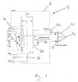
- a known "distributed amplifier” 10 is shown in Fig. 1, the architecture of which is shown generally at 12.
- Such distributed amplifiers are known, for example from US 6,130,423 assigned to Pixel Cam Inc., and US 6,084,229 assigned to Photon Vision Systems LLC.
- Distributed amplifiers are currently used to linearise a pixel source follower and/or to attenuate reset noise of a three transistor pixel.
- the present invention provides an image sensor in which all the components of the readout chain, that is the source follower (present for all active pixels), a sampling circuit, a preamplifier, and an analogue to digital conversion circuit, are combined in one single circuit.
- the functions of these components can be described as being integrated.
- a distributed amplifier is provided which is integrated with an ADC for noise reduction. This is achieved by using a pixel amplifier as a column comparator.
- the present invention pertains to image sensors formed from an array of active pixels.
- An active pixel may include a transfer gate, reset transistor and amplifying transistor, and may further optionally include a read transistor.
- the pixel has a photocurrent generating element which is preferably a photodiode, most preferably a pinned photodiode (In a pinned photodiode, the charge collection and charge to voltage conversion steps are separated. Charges are collected on a photodiode, and then transferred to a floating diffusion during readout).
- the invention is applicable to any type of image sensors formed from an array of active pixels, but has particular applicability for CMOS image sensors.
- the architecture 12 shows some components of an exemplary pixel 14 and some of an exemplary column circuit 16, as outlined.
- the amplifier 10 uses the pixel's amplifier transistor 18 as its positive (non-inverting) input 20.
- the negative (inverting) input 22 is provided from a transistor 24 in the column circuitry, while the load and current source are formed from other transistors (26 and 28 respectively) also located in the column circuitry.
- the output 30 of the amplifier 10 is also shown.
- Fig. 2 shows a first embodiment of the invention, where a number of amplifiers 10 are connected to a pixel array 32 made up of individual pixels 33.
- the amplifiers 10 are connected to the output lines Vx(i) and Vb(i) of each column 34 of the pixel array 32.
- Each amplifier 10 has a reset switch 36 connected between its inverting input 22 and output 30 operated by a global auto-zero signal AZ 42.
- AZ signal 42,66 goes high, the switch 36 is put into a first state whereby the amplifier is configured in unity gain feedback, and when the AZ signal 42,66 goes low, the switch 36 is put into a second state whereby the amplifier is configured in open loop and acts as a high gain comparator.
- the ramp generator 38 voltage couples via a capacitor Ccol 40 to the inverting input of the amplifier.
- the output 30 of each amplifier 10 is connected to a digital latch 44 and an n-bit memory element 46.
- the ramp voltage can be generated by any suitable means, such as a DAC.
- a clock 48 causes the analogue ramp voltage to decrease and simultaneously a digital Gray Code Count (GCC) 50 to increment.
- GCC Gray Code Count
- the amplifier 10 output voltage is converted to a digital state by the latch on each rising edge of the clock.
- a transition in the latch 44 output state causes the state of the GCC 50 at that time to be memorised in the RAM 46.
- the memorised state in each column RAM 46 is a measure of the size of the pixel voltage. Readout of the RAM is controlled by a horizontal shift register or decoder 52.
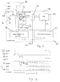
- Figs. 3 and 4 show the operation of a single column circuit of the array shown in Fig. 2.
- Labelled areas 56, 58 and 60 show which components are situated in the pixel, column circuits, and global circuits of the image sensor respectively.
- Components of Fig. 3 which correspond to those of Fig. 2 are illustrated with the same reference numerals.
- a READ signal 62 for a particular row of the pixel array 32 is asserted. This allows current to flow through the pixel amplifier transistor 18 and the amplifier 10 feedback loop is active. Then a RESET line 64 for that row of pixels 33 is pulsed and the voltage Vpix on the floating diffusion sense node is reset to a voltage VRST. Charge coupling and kT/C noise injection cause this voltage to depart from VRST on the falling edge of RESET 64.
- an autozero (AZ) signal 66 is pulsed.
- the ramp voltage is at some high level from which it may descend to adequately cover the expected output voltage swing of the pixel 33.
- the high state of AZ 66 causes the amplifier 10 to be in unity gain feedback such that the offset of the amplifier 10 is learnt on the column capacitor Ccol 40.
- the voltage on the capacitor Ccol 40 is (VRST - Vch - (kT/Cfd) 1/2 - Voffset - Vthermal), where Voffset is the amplifier 10 offset voltage (principally related to threshold (Vt) mismatch of the NMOS differential pair of the amplifier 10 , Vch is the charge coupling, Vthermal is the sampled thermal noise level of the amplifier 10, and Cfd is the floating diffusion capacitance.
- the amplifier 10 is in an open loop mode of operation.
- the AZ 66 falls, a certain amount of kT/C noise is sampled on the capacitor Ccol 40.
- the capacitor Ccol 40 is large compared to the floating diffusion capacitance and so this noise can effectively be disregarded.
- the transfer gate TG is pulsed 68 for the row of pixels 33.
- Charge is transferred from the pixel photodiode to the floating diffusion sense node Vpix causing it to decrease by a voltage Vsig related to the amount of light integrated on the photodiode during exposure.
- the aim of a pixel readout system is to convert this voltage to digital form with the minimum amount of additional noise due to the operation of the readout circuitry.
- the ramp voltage 70 generated by the ramp voltage generator 38 can be increased by a fixed offset Vdelta 72 to ensure that the negative input is greater than the positive input. Since the amplifier 10 is now open-loop it acts as a high gain comparator. The output voltage of the amplifier goes to 0V in response to the negative voltage difference at the amplifier inputs.
- the ramp now descends while a GCC 72 counts (the output 72 from the GCC 50 is illustrated in Fig. 4).
- the capacitor Ccol 40 causes the negative input of the amplifier 10 also to descend.
- the comparator output will change state (to AVDD) and the latch 44 will cause the GCC 72 value at this point to be memorised in the RAM 46.
- the pixel floating diffusion may integrate a small amount of light. It is normally shielded from light with metal (not shown) to minimise this effect.
- the input referred noise of a high gain comparator is very low and the ramp generator circuit noise may also be designed to make a minimal contribution.
- the noise contributed during actual ADC conversion is considered to be negligible compared to the noise during sampling.
- a prior art image sensor has a separate source follower and amplification step, both of which contribute 1/f noise and thermal noise.
- the above described embodiment combines the source follower and preamplifier in one circuit, so there is only one such contribution of noise rather than two.
- the quantiser is created by configuring the original amplifier after sampling as an open loop comparator.
- the quantiser 1/f noise is thus learnt and attenuated by the auto-zero step.
- sampling and autozero are combined into one operation. This eliminates one contribution of sampling (kT/C) noise and an extra noise introduced during an auto-zero step, both of which are present in prior art sensors. Furthermore, this combination means that only one sampling capacitor is required where two have previously been required, which reduces the on-chip area of the circuit.
- Fig. 6 shows another realization of a distributed amplifier employing a single stage operational transconductance amplifier structure. This amplifier produces a rail to rail output voltage range compatible with digital circuitry.
- Fig. 7 shows yet another implementation of a distributed amplifier using a folded cascode structure. This amplifier produces a rail to rail output voltage range compatible with digital circuitry.
- Fig. 8 shows a further implementation of a distributed amplifier, in which the Vb line is used to supply the pixel reset voltage.
- the ColReset signal goes low, overdriving the amplifier and setting Vb to VRST, the positive input can be set low during this time. Subsequent operation is unchanged from the system above.
- the image sensor of the present invention can be incorporated into a number of different products, including but not limited to a digital camera, an optical mouse, mobile telephone or webcam incorporating the digital camera, or other more specialised imagers used in diverse fields.
- a digital camera an optical mouse
- mobile telephone or webcam incorporating the digital camera
- other more specialised imagers used in diverse fields.
- the man skilled in the art will appreciate that the practical matter of implementing the invention in any of these or other devices is straightforward, and thus will not be described herein in more detail.
Landscapes
- Engineering & Computer Science (AREA)
- Multimedia (AREA)
- Signal Processing (AREA)
- Theoretical Computer Science (AREA)
- Transforming Light Signals Into Electric Signals (AREA)
- Solid State Image Pick-Up Elements (AREA)
Abstract
Description
- The present invention relates to improvements in or relating to image sensors, in particular to a new image sensor comprising pixel circuitry, readout circuitry and a distributed amplifier, and a method of sensing an image using the image sensor.
- A typical solid-state image sensor comprises a light gathering stage and a readout chain. An example of such a sensor is described in S. K. Mendis, S. E. Kemeny, R. C. Gee, B. Pain, C. O. Staller, Q. Kim, E. R. Fossum, "CMOS active pixel sensors for highly integrated imaging systems", IEEE J. Solid-State Circuits, vol. 32, pp. 187-197, Feb. 1997.
- The light gathering stage comprises a photodiode or other type of light sensitive element and a charge to voltage conversion means, while the readout chain typically comprises a source follower (present for all active pixels), a sampling circuit, a preamplifier, and an analogue to digital conversion circuit.
- Each of these components introduces noise to the detected image. The light contains photon shot noise, the photodiode introduces dark current shot noise, and fixed pattern noise, and the charge to voltage conversion means introduces transfer gate noise (pinned-photodiode pixels) or reset noise (3T active pixels).
- The aim of the readout chain is to convert the detected voltage to digital form with the minimum amount of additional noise. However, each component of the readout chain introduces noise to the process.
- The pixel source follower introduces both thermal and 1/f noise. The pixel transistors must be small to achieve a small pixel size and high fill factor and this compromises the noise level achievable. This noise source is often dominant over the remaining circuit noise.
- The sampling circuit is used to perform a double sampling step, using capacitors contained in the base of each pixel column. Two samples are taken and differenced to eliminate pixel source follower threshold (Vt) mismatch, which gives two contributions of kT/C noise. To achieve small chip sizes and fast readout times the size of the sampling capacitors is limited which therefore limits the minimum achievable noise level.
- Next, the preamplifier introduces thermal and 1/f noise. Often some means of removing amplifier column offsets is applied (auto-zero or feedback) which tends to increase this noise.
- Finally, the analogue to digital conversion circuit comprises a quantisation element, or quantiser, that introduces additional thermal noise, and a ramp generator that contributes quantisation noise and thermal noise. The quantisation element is required to convert from analogue to digital output levels and compare the input voltage levels with a ramp voltage.
- When designing an image sensor circuit, it is also desirable to minimise the surface area on the image sensor substrate that the circuit occupies. There is therefore often a trade-off between noise reduction and size considerations, for example, when considering the size (or capacitance) of capacitors to be used.
- Excessive noise degrades the performance of an image sensor, while an excessively large circuit will limit the applications to which the image sensor can be put or be commercially unattractive. It is therefore desirable to have a new image sensor that contributes less noise and that also makes efficient use of space.
- According to a first aspect of the present invention, there is provided an image sensor comprising pixel circuitry, readout circuitry and a distributed amplifier) which comprises a first input residing in the pixel circuitry, and a second input and output residing in the readout circuitry, and wherein the second input is coupled to a ramp voltage generator and the output is coupled to an analogue to digital conversion (ADC) means, characterised in that;
switch means are provided between the output and second input, said switch means being selectively operable by an autozero signal. - Preferably, the first input is a non-inverting input provided by a pixel amplifier transistor.
- Preferably, the second input is an inverting input that is coupled to the ramp generator via a column capacitor, and the switch means is selectively operable between a first state and a second state, wherein in the first state the switch causes the amplifier to be in closed loop operation and the offset of the amplifier is learnt on the column capacitor.
- Preferably, the closed loop operation uses a unity gain feedback.
- Preferably, when the switch means is in the second state, the amplifier is in an open loop mode operation such that it acts as a comparator.
- Preferably, the output is coupled to a digital latch which is in communication with a memory means.
- Preferably, the ADC is a single slope ADC.
- Preferably, the image sensor is a CMOS solid state image sensor.
- Preferably, the pixel circuitry comprises a photodiode, preferably a pinned photodiode.
- Preferably, a pixel source follower, sampling circuit, amplifier and ADC are all integrated in a single circuit.
- According to a second aspect of the present invention, there is provided an integrated circuit comprising an image sensor which comprises pixel circuitry, readout circuitry and a distributed amplifier which comprises a first input residing in the pixel circuitry, and a second input and output residing in the readout circuitry, and wherein the second input is coupled to a ramp voltage generator and the output is coupled to an analogue to digital conversion (ADC) means, characterised in that;
switch means are provided between the output and second input, said switch means being selectively operable by an autozero signal. - Preferable features of the first aspect may also be applied to the second aspect.
- According to a third aspect of the present invention, there is provided a digital camera comprising an image sensor which comprises pixel circuitry, readout circuitry and a distributed amplifier which comprises a first input residing in the pixel circuitry, and a second input and output residing in the readout circuitry, and wherein the second input is coupled to a ramp voltage generator and the output is coupled to an analogue to digital conversion (ADC) means, characterised in that;
switch means are provided between the output and second input, said switch means being selectively operable by an autozero signal. - Preferable features of the first aspect may also be applied to the third aspect.
- According to a fourth aspect of the present invention, there is provided a mobile telephone comprising the digital camera of the third aspect.
- According to a fifth aspect of the present invention, there is provided a webcam comprising the digital camera of the third aspect.
- According to a sixth aspect of the present invention, there is provided an optical mouse comprising the digital camera of the third aspect.
- According to a seventh aspect of the present invention, there is provided a method of sensing an image with an image sensor comprising pixel circuitry and readout circuitry, comprising the steps of
providing a distributed amplifier comprising a first input residing in the pixel circuitry, and a second input and output residing in the readout circuitry;
coupling the second input to a ramp voltage generator;
coupling the output to an analogue to digital conversion (ADC) means; and
selectively applying an autozero to operate a switch means provided between the output and second input. - Preferably, the first input is a non-inverting input provided by a pixel amplifier transistor.
- Preferably, the second input is an inverting input that is coupled to the ramp generator via a column capacitor, the method further comprising the steps of applying an autozero signal to put the switch means in a first state in which the amplifier operates in a closed loop mode of operation, and learning the offset of the amplifier on the column capacitor.
- Preferably, the closed loop operation uses a unity gain feedback.
- Preferably, the method further comprises the steps of switching off the autozero signal, and operating the amplifier in an open loop operation in which the amplifier acts as a comparator.
- Preferably, the step of coupling the output to an analogue to digital conversion (ADC) means comprises coupling the output to a digital latch which is in communication with a memory means.
- Preferably, the ADC is a single slope ADC.
- Preferably, the image sensor is a CMOS solid state image sensor.
- Preferably, the pixel circuitry comprises a photodiode, preferably a pinned photodiode.
- Preferably, a pixel source follower, sampling circuit, amplifier and ADC are all integrated in a single circuit.
- The present invention will now be described, by way of example only, with reference to the accompanying drawings, in which:
- Fig. 1 illustrates a prior art distributed amplifier;
- Fig. 2 illustrates part of an image sensor architecture according to a first embodiment of the invention, wherein the distributed amplifier of Fig. 1 is connected to an exemplary pixel array;
- Fig. 3 shows details of a selection of components shown in Fig. 2;
- Fig. 4 illustrates the operation of the components of Fig. 3;
- Fig. 5 illustrates an image sensor architecture according to a second embodiment of the invention, wherein a distributed amplifier is used to achieve a rail to rail output;
- Fig. 6 illustrates an image sensor architecture according to a third embodiment of the invention, wherein a distributed amplifier is used to achieve an alternative rail to rail output;
- Fig. 7 illustrates an image sensor architecture according to a fourth embodiment of the invention, wherein a distributed amplifier is used to achieve a folded cascode circuit; and
- Fig. 8 illustrates an image sensor architecture according to a fifth embodiment of the invention, wherein a distributed amplifier is used with column-wise pixel reset voltage.
- A known "distributed amplifier" 10 is shown in Fig. 1, the architecture of which is shown generally at 12. Such distributed amplifiers are known, for example from US 6,130,423 assigned to Pixel Cam Inc., and US 6,084,229 assigned to Photon Vision Systems LLC.
- Distributed amplifiers are currently used to linearise a pixel source follower and/or to attenuate reset noise of a three transistor pixel.
- The present invention provides an image sensor in which all the components of the readout chain, that is the source follower (present for all active pixels), a sampling circuit, a preamplifier, and an analogue to digital conversion circuit, are combined in one single circuit. In this circuit, the functions of these components can be described as being integrated. In particular, a distributed amplifier is provided which is integrated with an ADC for noise reduction. This is achieved by using a pixel amplifier as a column comparator.
- The present invention pertains to image sensors formed from an array of active pixels. An active pixel may include a transfer gate, reset transistor and amplifying transistor, and may further optionally include a read transistor. The pixel has a photocurrent generating element which is preferably a photodiode, most preferably a pinned photodiode (In a pinned photodiode, the charge collection and charge to voltage conversion steps are separated. Charges are collected on a photodiode, and then transferred to a floating diffusion during readout). The invention is applicable to any type of image sensors formed from an array of active pixels, but has particular applicability for CMOS image sensors.
- Referring again to Fig. 1, the
architecture 12 shows some components of anexemplary pixel 14 and some of anexemplary column circuit 16, as outlined. - The
amplifier 10 uses the pixel'samplifier transistor 18 as its positive (non-inverting)input 20. The negative (inverting)input 22 is provided from atransistor 24 in the column circuitry, while the load and current source are formed from other transistors (26 and 28 respectively) also located in the column circuitry. Theoutput 30 of theamplifier 10 is also shown. - Fig. 2 shows a first embodiment of the invention, where a number of
amplifiers 10 are connected to apixel array 32 made up ofindividual pixels 33. Theamplifiers 10 are connected to the output lines Vx(i) and Vb(i) of eachcolumn 34 of thepixel array 32. Eachamplifier 10 has areset switch 36 connected between its invertinginput 22 andoutput 30 operated by a global auto-zerosignal AZ 42. When theAZ signal 42,66 goes high, theswitch 36 is put into a first state whereby the amplifier is configured in unity gain feedback, and when theAZ signal 42,66 goes low, theswitch 36 is put into a second state whereby the amplifier is configured in open loop and acts as a high gain comparator. Theramp generator 38 voltage couples via acapacitor Ccol 40 to the inverting input of the amplifier. Theoutput 30 of eachamplifier 10 is connected to adigital latch 44 and an n-bit memory element 46. - The ramp voltage can be generated by any suitable means, such as a DAC. A
clock 48 causes the analogue ramp voltage to decrease and simultaneously a digital Gray Code Count (GCC) 50 to increment. Theamplifier 10 output voltage is converted to a digital state by the latch on each rising edge of the clock. A transition in thelatch 44 output state causes the state of theGCC 50 at that time to be memorised in theRAM 46. The memorised state in eachcolumn RAM 46 is a measure of the size of the pixel voltage. Readout of the RAM is controlled by a horizontal shift register ordecoder 52. - Figs. 3 and 4 show the operation of a single column circuit of the array shown in Fig. 2. Labelled
areas - A method of operation of the circuit of Fig. 3 will now be described. Firstly, a
READ signal 62 for a particular row of thepixel array 32 is asserted. This allows current to flow through thepixel amplifier transistor 18 and theamplifier 10 feedback loop is active. Then aRESET line 64 for that row ofpixels 33 is pulsed and the voltage Vpix on the floating diffusion sense node is reset to a voltage VRST. Charge coupling and kT/C noise injection cause this voltage to depart from VRST on the falling edge ofRESET 64. - Next, an autozero (AZ) signal 66 is pulsed. The ramp voltage is at some high level from which it may descend to adequately cover the expected output voltage swing of the
pixel 33. The high state of AZ 66 causes theamplifier 10 to be in unity gain feedback such that the offset of theamplifier 10 is learnt on thecolumn capacitor Ccol 40. - On the falling edge of AZ 66, the voltage on the
capacitor Ccol 40 is (VRST - Vch - (kT/Cfd)1/2 - Voffset - Vthermal), where Voffset is theamplifier 10 offset voltage (principally related to threshold (Vt) mismatch of the NMOS differential pair of theamplifier 10 , Vch is the charge coupling, Vthermal is the sampled thermal noise level of theamplifier 10, and Cfd is the floating diffusion capacitance. - Then, with AZ in a low state, the
amplifier 10 is in an open loop mode of operation. When the AZ 66 falls, a certain amount of kT/C noise is sampled on thecapacitor Ccol 40. However thecapacitor Ccol 40 is large compared to the floating diffusion capacitance and so this noise can effectively be disregarded. - Next, the transfer gate TG is pulsed 68 for the row of
pixels 33. Charge is transferred from the pixel photodiode to the floating diffusion sense node Vpix causing it to decrease by a voltage Vsig related to the amount of light integrated on the photodiode during exposure. - The aim of a pixel readout system is to convert this voltage to digital form with the minimum amount of additional noise due to the operation of the readout circuitry. At this point the ramp voltage 70 generated by the
ramp voltage generator 38 can be increased by a fixed offsetVdelta 72 to ensure that the negative input is greater than the positive input. Since theamplifier 10 is now open-loop it acts as a high gain comparator. The output voltage of the amplifier goes to 0V in response to the negative voltage difference at the amplifier inputs. - The ramp now descends while a
GCC 72 counts (theoutput 72 from theGCC 50 is illustrated in Fig. 4). Thecapacitor Ccol 40 causes the negative input of theamplifier 10 also to descend. When the negative input has moved by an amount (Vdelta + Vsig) the comparator output will change state (to AVDD) and thelatch 44 will cause theGCC 72 value at this point to be memorised in theRAM 46. During the descent of the ramp 70 the pixel floating diffusion may integrate a small amount of light. It is normally shielded from light with metal (not shown) to minimise this effect. - The capacitor noise sqrt(kT/Ccol) and Vthermal are not compensated by this scheme and so contribute to the noise floor of the converter. However, the amplifier offset voltage Voffset and sqrt(kT/Cfd) are learnt and removed.
- Moreover, the input referred noise of a high gain comparator is very low and the ramp generator circuit noise may also be designed to make a minimal contribution. Thus, the noise contributed during actual ADC conversion is considered to be negligible compared to the noise during sampling.
- The noise contribution of the above described embodiments is reduced for the foregoing reasons.
- As described above, a prior art image sensor has a separate source follower and amplification step, both of which contribute 1/f noise and thermal noise. However, the above described embodiment combines the source follower and preamplifier in one circuit, so there is only one such contribution of noise rather than two.
- The quantiser is created by configuring the original amplifier after sampling as an open loop comparator. The
quantiser 1/f noise is thus learnt and attenuated by the auto-zero step. - Also as described above, sampling and autozero are combined into one operation. This eliminates one contribution of sampling (kT/C) noise and an extra noise introduced during an auto-zero step, both of which are present in prior art sensors. Furthermore, this combination means that only one sampling capacitor is required where two have previously been required, which reduces the on-chip area of the circuit.
- The elimination of a separate column preamplifier also results in a space saving.
- These and other advantages are also shown in alternative embodiments of the invention, some examples of which are shown in Figs. 6-8. It will be appreciated that other amplifier configurations will be obvious to those skilled in the art.
- Fig. 6 shows another realization of a distributed amplifier employing a single stage operational transconductance amplifier structure. This amplifier produces a rail to rail output voltage range compatible with digital circuitry.
- Fig. 7 shows yet another implementation of a distributed amplifier using a folded cascode structure. This amplifier produces a rail to rail output voltage range compatible with digital circuitry.
- Fig. 8 shows a further implementation of a distributed amplifier, in which the Vb line is used to supply the pixel reset voltage. The ColReset signal goes low, overdriving the amplifier and setting Vb to VRST, the positive input can be set low during this time. Subsequent operation is unchanged from the system above.
- Various modifications and improvements can be made to the above without departing from the scope of the present invention. For example, the above embodiments are described with reference to a single ramp ADC. However, the invention is equally applicable to a double or other multiple ramp ADC. The invention also has applicability to CMOS, CCD or other types of solid state image sensors, the pixel used in an image sensor of the invention could be any type of active or passive pixel, and can have any type of photocurrent generating element.
- It will also be appreciated that the image sensor of the present invention can be incorporated into a number of different products, including but not limited to a digital camera, an optical mouse, mobile telephone or webcam incorporating the digital camera, or other more specialised imagers used in diverse fields. The man skilled in the art will appreciate that the practical matter of implementing the invention in any of these or other devices is straightforward, and thus will not be described herein in more detail.
Claims (25)
- An image sensor comprising pixel circuitry (56), readout circuitry (58,60) and a distributed amplifier (10) which comprises a first input (20) residing in the pixel circuitry (56), and a second input (22) and output (30) residing in the readout circuitry (58,60), and wherein the second input (22) is coupled to a ramp voltage generator (38) and the output (30) is coupled to an analogue to digital conversion (ADC) means, characterised in that;
switch means (36) are provided between the output (30) and second input (22), said switch means (36) being selectively operable by an autozero signal (66). - The image sensor of claim 1, wherein the first input (20) is a non-inverting input provided by a pixel amplifier transistor (18).
- The image sensor of claim 1 or claim 2, wherein the second input (22) is an inverting input that is coupled to the ramp generator (38) via a column capacitor (40), and the switch means (36) is selectively operable between a first state and a second state, wherein in the first state the switch (36) causes the amplifier (10) to be in closed loop operation and the offset of the amplifier (10) is learnt on the column capacitor (40).
- The image sensor of claim 3, wherein the closed loop operation uses a unity gain feedback.
- The image sensor of any of claims 2 to 4, wherein, when the switch means is in the second state, the amplifier (10) is in an open loop mode operation such that it acts as a comparator.
- The image sensor of any preceding claim, wherein the output (30) is coupled to a digital latch (44) which is in communication with a memory means (46).
- The image sensor of any preceding claim, wherein the ADC is a single slope ADC.
- The image sensor of any preceding claim, wherein the image sensor is a CMOS solid state image sensor.
- The image sensor of any preceding claim, wherein the pixel circuitry (56) comprises a photodiode (76), preferably a pinned photodiode.
- The image sensor of any preceding claim, wherein a pixel source follower, sampling circuit, amplifier and ADC are all integrated in a single circuit.
- An integrated circuit comprising an image sensor which comprises pixel circuitry (56), readout circuitry (58,60) and a distributed amplifier (10) which comprises a first input (20) residing in the pixel circuitry (56), and a second input (22) and output (30) residing in the readout circuitry (58,60), and wherein the second input (22) is coupled to a ramp voltage generator (38) and the output (30) is coupled to an analogue to digital conversion (ADC) means, characterised in that;
switch means (36) are provided between the output (30) and second input (22), said switch means (36) being selectively operable by an autozero signal (66). - A digital camera comprising an image sensor which comprises pixel circuitry (56), readout circuitry (58,60) and a distributed amplifier (10) which comprises a first input (20) residing in the pixel circuitry (56), and a second input (22) and output (30) residing in the readout circuitry (58,60), and wherein the second input (22) is coupled to a ramp voltage generator (38) and the output (30) is coupled to an analogue to digital conversion (ADC) means, characterised in that;
switch means (36) are provided between the output (30) and second input (22), said switch means (36) being selectively operable by an autozero signal (66). - A mobile telephone comprising the digital camera of claim 12.
- A webcam comprising the digital camera of claim 12.
- An optical mouse comprising the digital camera of claim 12.
- A method of sensing an image with an image sensor comprising pixel circuitry (56) and readout circuitry (58), comprising the steps of
providing a distributed amplifier (10) comprising a first input (22) residing in the pixel circuitry (56), and a second input (20) and output (30) residing in the readout circuitry (58);
coupling the second input (22) to a ramp voltage generator (38);
coupling the output (30) to an analogue to digital conversion (ADC) means; and
selectively applying an autozero (66) to operate a switch means (36) provided between the output (30) and second input (22). - The method of claim 16, wherein the first input (20) is a non-inverting input provided by a pixel amplifier transistor (18).
- The method of claim 16 or claim 17, wherein the second input (22) is an inverting input that is coupled to the ramp generator (38) via a column capacitor (40), the method further comprising the steps of applying an autozero signal (66) to put the switch means (36) in a first state in which the amplifier (10) operates in a closed loop mode of operation, and learning the offset of the amplifier (10) on the column capacitor (40).
- The method of claim 18, wherein the closed loop operation uses a unity gain feedback.
- The method of any of claims 16 to 19, further comprising the steps of switching off the autozero signal (66), and operating the amplifier (10) in an open loop operation in which the amplifier (10) acts as a comparator.
- The method of any of claims 16 to 20, wherein the step of coupling the output (30) to an analogue to digital conversion (ADC) means comprises coupling the output (30) to a digital latch (44) which is in communication with a memory means (46).
- The method of any of claims 16 to 21, wherein the ADC is a single slope ADC.
- The method of any of claims 16 to 22, wherein the image sensor is a CMOS solid state image sensor.
- The method of any of claims 16 to 23, wherein the pixel circuitry comprises a photodiode, preferably a pinned photodiode.
- The method of any of claims 16 to 24, wherein a pixel source follower, sampling circuit, amplifier and ADC are all integrated in a single circuit.
Priority Applications (2)
| Application Number | Priority Date | Filing Date | Title |
|---|---|---|---|
| EP04255476A EP1635470A1 (en) | 2004-09-09 | 2004-09-09 | Method and apparatus for a CMOS image sensor comprising a distributed amplifier and a multiplexed analog to digital converter |
| US11/223,558 US7265329B2 (en) | 2004-09-09 | 2005-09-09 | Image sensors with distributed amplifiers and related methods |
Applications Claiming Priority (1)
| Application Number | Priority Date | Filing Date | Title |
|---|---|---|---|
| EP04255476A EP1635470A1 (en) | 2004-09-09 | 2004-09-09 | Method and apparatus for a CMOS image sensor comprising a distributed amplifier and a multiplexed analog to digital converter |
Publications (1)
| Publication Number | Publication Date |
|---|---|
| EP1635470A1 true EP1635470A1 (en) | 2006-03-15 |
Family
ID=34930640
Family Applications (1)
| Application Number | Title | Priority Date | Filing Date |
|---|---|---|---|
| EP04255476A Ceased EP1635470A1 (en) | 2004-09-09 | 2004-09-09 | Method and apparatus for a CMOS image sensor comprising a distributed amplifier and a multiplexed analog to digital converter |
Country Status (2)
| Country | Link |
|---|---|
| US (1) | US7265329B2 (en) |
| EP (1) | EP1635470A1 (en) |
Cited By (6)
| Publication number | Priority date | Publication date | Assignee | Title |
|---|---|---|---|---|
| EP1956715A1 (en) * | 2007-02-08 | 2008-08-13 | STMicroelectronics (Research & Development) Limited | Analogue to digital converter |
| CN101237236B (en) * | 2007-01-30 | 2010-06-02 | 夏普株式会社 | A/d converter |
| US9093998B2 (en) | 2013-07-17 | 2015-07-28 | Taiwan Semiconductor Manufacturing Co., Ltd. | Method and apparatus for generating a ramp signal |
| US9385260B2 (en) | 2013-07-10 | 2016-07-05 | Tsmc Solar Ltd. | Apparatus and methods for forming thin film solar cell materials |
| CN106027923A (en) * | 2015-03-30 | 2016-10-12 | 佳能株式会社 | Photoelectric conversion apparatus and photoelectric conversion system |
| WO2017134969A1 (en) * | 2016-02-03 | 2017-08-10 | Sony Corporation | Image sensor and electronic device with active reset circuit, and method of operating the same |
Families Citing this family (18)
| Publication number | Priority date | Publication date | Assignee | Title |
|---|---|---|---|---|
| US7148831B2 (en) * | 2003-10-27 | 2006-12-12 | Micron Technology, Inc. | Variable quantization ADC for image sensors |
| KR100744117B1 (en) * | 2005-08-24 | 2007-08-01 | 삼성전자주식회사 | Image sensor and manufacturing method with lossless nonlinear analog gain controller |
| US20070236590A1 (en) * | 2006-03-31 | 2007-10-11 | Cypress Semiconductor Corporation | Output auto-zero for CMOS active pixel sensors |
| US7791664B1 (en) * | 2006-07-20 | 2010-09-07 | Advasense Technologies Ltd. | Methods for reading a pixel and for writing to a pixel and a device having pixel reading capabilities and pixel writing capabilities |
| JP5123601B2 (en) * | 2006-08-31 | 2013-01-23 | キヤノン株式会社 | Photoelectric conversion device |
| US7969476B1 (en) * | 2007-05-24 | 2011-06-28 | Advasense Technologies Ltd. | Method for accessing a pixel and a device having pixel access capabilities |
| US7889257B2 (en) * | 2007-07-18 | 2011-02-15 | Mesa Imaging Ag | On-chip time-based digital conversion of pixel outputs |
| JP5434502B2 (en) * | 2009-11-13 | 2014-03-05 | ソニー株式会社 | Solid-state imaging device, driving method thereof, and camera system |
| JP5704939B2 (en) * | 2011-01-31 | 2015-04-22 | オリンパス株式会社 | Imaging device |
| US8624769B2 (en) * | 2011-08-11 | 2014-01-07 | California Institute Of Technology | Mixed linear/square-root encoded single slope ramp provides a fast, low noise analog to digital converter with very high linearity for focal plane arrays |
| JP6019870B2 (en) * | 2012-07-20 | 2016-11-02 | ソニー株式会社 | Solid-state imaging device and manufacturing method |
| JP2015115745A (en) * | 2013-12-11 | 2015-06-22 | ソニー株式会社 | Solid-state imaging device, imaging device, and electronic device |
| KR102245973B1 (en) | 2014-02-17 | 2021-04-29 | 삼성전자주식회사 | Correlated double sampling circuit and image sensor including the same |
| KR20160121189A (en) | 2015-04-10 | 2016-10-19 | 삼성전자주식회사 | Image Sensor For Improving Linearity of Analog-to-Digital Converter and image Processing System Including The Same |
| JP6632421B2 (en) * | 2016-02-22 | 2020-01-22 | キヤノン株式会社 | Solid-state imaging device and imaging device |
| KR102510671B1 (en) * | 2018-09-21 | 2023-03-20 | 에스케이하이닉스 주식회사 | Ramp signal generator and image sensor including the same |
| CN111918003B (en) * | 2019-05-08 | 2022-11-25 | 上海耕岩智能科技有限公司 | Image sensor, signal acquisition method and circuit thereof, storage medium and terminal |
| US10924701B2 (en) * | 2019-07-18 | 2021-02-16 | Omnivision Technologies, Inc. | Column amplifier reset circuit with comparator |
Citations (6)
| Publication number | Priority date | Publication date | Assignee | Title |
|---|---|---|---|---|
| US5801657A (en) * | 1997-02-05 | 1998-09-01 | Stanford University | Serial analog-to-digital converter using successive comparisons |
| US6310571B1 (en) * | 2001-03-30 | 2001-10-30 | Pixim, Incorporated | Multiplexed multi-channel bit serial analog-to-digital converter |
| US6369737B1 (en) * | 1997-10-30 | 2002-04-09 | The Board Of Trustees Of The Leland Stanford Junior University | Method and apparatus for converting a low dynamic range analog signal to a large dynamic range floating-point digital representation |
| US6380880B1 (en) * | 2001-03-30 | 2002-04-30 | Pixim, Incorporated | Digital pixel sensor with integrated charge transfer amplifier |
| US6693575B1 (en) * | 2001-03-30 | 2004-02-17 | Pixim, Inc. | Multi-channel bit-serial analog-to-digital converter with reduced channel circuitry |
| EP1391932A1 (en) * | 2002-08-22 | 2004-02-25 | STMicroelectronics Limited | Solid state image sensor |
Family Cites Families (8)
| Publication number | Priority date | Publication date | Assignee | Title |
|---|---|---|---|---|
| JPH10108081A (en) | 1996-10-02 | 1998-04-24 | Sony Corp | Solid-state imaging device, signal processing method thereof, and camera |
| US6515701B2 (en) | 1997-07-24 | 2003-02-04 | Polaroid Corporation | Focal plane exposure control system for CMOS area image sensors |
| GB2334848B (en) * | 1998-02-28 | 2000-04-19 | Hyundai Electronics Ind | CMOS image sensor with testing circuit for verifying operation thereof |
| US6215113B1 (en) * | 1999-04-22 | 2001-04-10 | National Science Council | CMOS active pixel sensor |
| US6529152B1 (en) * | 1999-10-15 | 2003-03-04 | Cyngal Integrated Products, Inc. | High precision SAR converter using resistor strip with auto zeroing function |
| US6545624B2 (en) * | 2000-02-11 | 2003-04-08 | Hyundai Electronics Industries Co., Ltd. | Image sensor with analog-to-digital converter that generates a variable slope ramp signal |
| US6670904B1 (en) * | 2002-08-22 | 2003-12-30 | Micron Technology, Inc. | Double-ramp ADC for CMOS sensors |
| US7382407B2 (en) | 2002-08-29 | 2008-06-03 | Micron Technology, Inc. | High intrascene dynamic range NTSC and PAL imager |
-
2004
- 2004-09-09 EP EP04255476A patent/EP1635470A1/en not_active Ceased
-
2005
- 2005-09-09 US US11/223,558 patent/US7265329B2/en not_active Expired - Lifetime
Patent Citations (6)
| Publication number | Priority date | Publication date | Assignee | Title |
|---|---|---|---|---|
| US5801657A (en) * | 1997-02-05 | 1998-09-01 | Stanford University | Serial analog-to-digital converter using successive comparisons |
| US6369737B1 (en) * | 1997-10-30 | 2002-04-09 | The Board Of Trustees Of The Leland Stanford Junior University | Method and apparatus for converting a low dynamic range analog signal to a large dynamic range floating-point digital representation |
| US6310571B1 (en) * | 2001-03-30 | 2001-10-30 | Pixim, Incorporated | Multiplexed multi-channel bit serial analog-to-digital converter |
| US6380880B1 (en) * | 2001-03-30 | 2002-04-30 | Pixim, Incorporated | Digital pixel sensor with integrated charge transfer amplifier |
| US6693575B1 (en) * | 2001-03-30 | 2004-02-17 | Pixim, Inc. | Multi-channel bit-serial analog-to-digital converter with reduced channel circuitry |
| EP1391932A1 (en) * | 2002-08-22 | 2004-02-25 | STMicroelectronics Limited | Solid state image sensor |
Cited By (14)
| Publication number | Priority date | Publication date | Assignee | Title |
|---|---|---|---|---|
| CN101237236B (en) * | 2007-01-30 | 2010-06-02 | 夏普株式会社 | A/d converter |
| EP1956715A1 (en) * | 2007-02-08 | 2008-08-13 | STMicroelectronics (Research & Development) Limited | Analogue to digital converter |
| US8054210B2 (en) | 2007-02-08 | 2011-11-08 | Stmicroelectronics (Research & Development) Limited | Analog to digital converter |
| US9385260B2 (en) | 2013-07-10 | 2016-07-05 | Tsmc Solar Ltd. | Apparatus and methods for forming thin film solar cell materials |
| US9093998B2 (en) | 2013-07-17 | 2015-07-28 | Taiwan Semiconductor Manufacturing Co., Ltd. | Method and apparatus for generating a ramp signal |
| EP3076663A3 (en) * | 2015-03-30 | 2016-12-28 | Canon Kabushiki Kaisha | Photoelectric conversion apparatus and photoelectric conversion system |
| CN106027923A (en) * | 2015-03-30 | 2016-10-12 | 佳能株式会社 | Photoelectric conversion apparatus and photoelectric conversion system |
| US9813649B2 (en) | 2015-03-30 | 2017-11-07 | Canon Kabushiki Kaisha | Photoelectric conversion apparatus and photoelectric conversion system |
| RU2638914C2 (en) * | 2015-03-30 | 2017-12-18 | Кэнон Кабусики Кайся | Photoelectric conversion device and photoelectric conversion system |
| US10142573B2 (en) | 2015-03-30 | 2018-11-27 | Canon Kabushiki Kaisha | Photoelectric conversion apparatus and photoelectric conversion system |
| CN106027923B (en) * | 2015-03-30 | 2019-07-12 | 佳能株式会社 | Photoelectric conversion device and photo-translating system |
| WO2017134969A1 (en) * | 2016-02-03 | 2017-08-10 | Sony Corporation | Image sensor and electronic device with active reset circuit, and method of operating the same |
| US10110841B2 (en) | 2016-02-03 | 2018-10-23 | Sony Corporation | Image sensor and electronic device with active reset circuit, and method of operating the same |
| US10659714B2 (en) | 2016-02-03 | 2020-05-19 | Sony Corporation | Image sensor and electronic device with active reset circuit, and method of operating the same |
Also Published As
| Publication number | Publication date |
|---|---|
| US7265329B2 (en) | 2007-09-04 |
| US20060049334A1 (en) | 2006-03-09 |
Similar Documents
| Publication | Publication Date | Title |
|---|---|---|
| US7265329B2 (en) | Image sensors with distributed amplifiers and related methods | |
| US8462243B2 (en) | Solid-state image sensing device, method for reading signal of solid-state image sensing device, and image pickup apparatus | |
| CN102859996B (en) | Solid camera head and driving method, camera | |
| US7468501B2 (en) | Linear dynamic range enhancement in a CMOS imager | |
| CN109040630B (en) | Ramp signal generator of image sensor and image sensor including the same | |
| KR101969189B1 (en) | Solid-state image sensor and camera system | |
| US9088741B2 (en) | Method of controlling semiconductor device, signal processing method, semiconductor device, and electronic apparatus | |
| US8330843B2 (en) | Solid-state image sensing device, method for driving solid-state image sensing device, and image sensing system incorporated with solid-state image sensing device | |
| US8063964B2 (en) | Dual sensitivity image sensor | |
| US6818933B2 (en) | CMOS image sensors | |
| US10116890B2 (en) | Imaging apparatus and imaging method using difference between reset signal and pixel signal stored to two capacitors | |
| US8324548B2 (en) | Imaging devices and methods for charge transfer | |
| KR20240039141A (en) | Pixel arrays, image sensors, and methods of operating pixel arrays | |
| KR20110109891A (en) | Solid-state imaging device, signal processing method of solid-state imaging device, and electronic device | |
| US7408138B2 (en) | Analog-to-digital converter with noise compensation in CMOS image sensor | |
| US7830425B2 (en) | Areal active pixel image sensor with programmable row-specific gain for hyper-spectral imaging | |
| EP2005731A1 (en) | A/d converter using ramped transfer gate clocks | |
| US20090251572A1 (en) | Efficient wide-range and high-resolution black level and offset calibration system | |
| WO2007016320A2 (en) | Cmos imager with wide dynamic range pixel | |
| US12452563B2 (en) | Solid-state imaging device, method for driving solid-state imaging device, and electronic apparatus | |
| Meynants et al. | Welcome to the world of single-slope column-level analog-to-digital converters for cmos image sensors | |
| CN115665574B (en) | A pixel circuit and a noise reduction method | |
| JP2011091724A (en) | Solid state imaging device | |
| Park et al. | An ultra wide dynamic range cmos image sensor with a linear response | |
| US20030001079A1 (en) | Current mode pixel amplifier |
Legal Events
| Date | Code | Title | Description |
|---|---|---|---|
| PUAI | Public reference made under article 153(3) epc to a published international application that has entered the european phase |
Free format text: ORIGINAL CODE: 0009012 |
|
| AK | Designated contracting states |
Kind code of ref document: A1 Designated state(s): AT BE BG CH CY CZ DE DK EE ES FI FR GB GR HU IE IT LI LU MC NL PL PT RO SE SI SK TR |
|
| AX | Request for extension of the european patent |
Extension state: AL HR LT LV MK |
|
| 17P | Request for examination filed |
Effective date: 20060829 |
|
| AKX | Designation fees paid |
Designated state(s): DE FR GB IT |
|
| 17Q | First examination report despatched |
Effective date: 20070822 |
|
| RAP1 | Party data changed (applicant data changed or rights of an application transferred) |
Owner name: STMICROELECTRONICS (RESEARCH & DEVELOPMENT) LIMITE |
|
| STAA | Information on the status of an ep patent application or granted ep patent |
Free format text: STATUS: THE APPLICATION HAS BEEN REFUSED |
|
| 18R | Application refused |
Effective date: 20110217 |