EP1635321A2 - Plasma display apparatus including an energy recovery circuit - Google Patents
Plasma display apparatus including an energy recovery circuit Download PDFInfo
- Publication number
- EP1635321A2 EP1635321A2 EP05255466A EP05255466A EP1635321A2 EP 1635321 A2 EP1635321 A2 EP 1635321A2 EP 05255466 A EP05255466 A EP 05255466A EP 05255466 A EP05255466 A EP 05255466A EP 1635321 A2 EP1635321 A2 EP 1635321A2
- Authority
- EP
- European Patent Office
- Prior art keywords
- voltage
- energy
- recovery
- supply
- unit
- Prior art date
- Legal status (The legal status is an assumption and is not a legal conclusion. Google has not performed a legal analysis and makes no representation as to the accuracy of the status listed.)
- Withdrawn
Links
Images




Classifications
-
- G—PHYSICS
- G09—EDUCATION; CRYPTOGRAPHY; DISPLAY; ADVERTISING; SEALS
- G09G—ARRANGEMENTS OR CIRCUITS FOR CONTROL OF INDICATING DEVICES USING STATIC MEANS TO PRESENT VARIABLE INFORMATION
- G09G3/00—Control arrangements or circuits, of interest only in connection with visual indicators other than cathode-ray tubes
- G09G3/20—Control arrangements or circuits, of interest only in connection with visual indicators other than cathode-ray tubes for presentation of an assembly of a number of characters, e.g. a page, by composing the assembly by combination of individual elements arranged in a matrix no fixed position being assigned to or needed to be assigned to the individual characters or partial characters
- G09G3/22—Control arrangements or circuits, of interest only in connection with visual indicators other than cathode-ray tubes for presentation of an assembly of a number of characters, e.g. a page, by composing the assembly by combination of individual elements arranged in a matrix no fixed position being assigned to or needed to be assigned to the individual characters or partial characters using controlled light sources
- G09G3/28—Control arrangements or circuits, of interest only in connection with visual indicators other than cathode-ray tubes for presentation of an assembly of a number of characters, e.g. a page, by composing the assembly by combination of individual elements arranged in a matrix no fixed position being assigned to or needed to be assigned to the individual characters or partial characters using controlled light sources using luminous gas-discharge panels, e.g. plasma panels
- G09G3/288—Control arrangements or circuits, of interest only in connection with visual indicators other than cathode-ray tubes for presentation of an assembly of a number of characters, e.g. a page, by composing the assembly by combination of individual elements arranged in a matrix no fixed position being assigned to or needed to be assigned to the individual characters or partial characters using controlled light sources using luminous gas-discharge panels, e.g. plasma panels using AC panels
- G09G3/296—Driving circuits for producing the waveforms applied to the driving electrodes
- G09G3/2965—Driving circuits for producing the waveforms applied to the driving electrodes using inductors for energy recovery
-
- G—PHYSICS
- G09—EDUCATION; CRYPTOGRAPHY; DISPLAY; ADVERTISING; SEALS
- G09G—ARRANGEMENTS OR CIRCUITS FOR CONTROL OF INDICATING DEVICES USING STATIC MEANS TO PRESENT VARIABLE INFORMATION
- G09G3/00—Control arrangements or circuits, of interest only in connection with visual indicators other than cathode-ray tubes
- G09G3/20—Control arrangements or circuits, of interest only in connection with visual indicators other than cathode-ray tubes for presentation of an assembly of a number of characters, e.g. a page, by composing the assembly by combination of individual elements arranged in a matrix no fixed position being assigned to or needed to be assigned to the individual characters or partial characters
- G09G3/22—Control arrangements or circuits, of interest only in connection with visual indicators other than cathode-ray tubes for presentation of an assembly of a number of characters, e.g. a page, by composing the assembly by combination of individual elements arranged in a matrix no fixed position being assigned to or needed to be assigned to the individual characters or partial characters using controlled light sources
- G09G3/28—Control arrangements or circuits, of interest only in connection with visual indicators other than cathode-ray tubes for presentation of an assembly of a number of characters, e.g. a page, by composing the assembly by combination of individual elements arranged in a matrix no fixed position being assigned to or needed to be assigned to the individual characters or partial characters using controlled light sources using luminous gas-discharge panels, e.g. plasma panels
- G09G3/288—Control arrangements or circuits, of interest only in connection with visual indicators other than cathode-ray tubes for presentation of an assembly of a number of characters, e.g. a page, by composing the assembly by combination of individual elements arranged in a matrix no fixed position being assigned to or needed to be assigned to the individual characters or partial characters using controlled light sources using luminous gas-discharge panels, e.g. plasma panels using AC panels
- G09G3/296—Driving circuits for producing the waveforms applied to the driving electrodes
Definitions
- the present invention relates a plasma display apparatus, and more particularly to a plasma display apparatus including an energy recovery circuit.
- FIG. 1 is a view illustrating a method of representing an image gray level of a conventional plasma display panel.
- the image gray level is derived by dividing one frame into a number of sub fields whose number of the emission of light is different from each other.
- Each sub field is divided into a reset section which is to uniformly generate a discharge, an address section which is to select a discharge cell, and a sustain section which is to implement the gray level depending on the number of discharge.
- a frame section (16.67ms) corresponding to 1/60 sec is divided into 8 sub fields so as to display an image with 256 gray levels.
- each of 8 sub fields is divided again into an address section and a sustain section.
- a driving device for driving the plasma display panel includes a driving device which applies alternate sustain voltage (Vs) to a Y electrode and a Z electrode in order to maintain the discharge of cell which is selected during the sustain period.
- Vs alternate sustain voltage
- Such a driving device for driving the plasma display panel is included in a Y electrode driving unit and a Z electrode driving unit, respectively, the driving device for driving the plasma display panel included in each driving unit is as shown in FIG. 3.
- FIG. 2 is a construction of a driving device of a conventional plasma display panel.
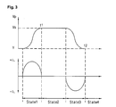
- FIG. 3 is a pulse form formed by a conventional energy recovery circuit. As shown in FIGS. 2 and 3, the conventional driving device for driving the plasma display panel utilizes a energy recovery circuit to recover the unnecessarily generated energy, i.e. the reactive power, in the panel.
- a first switch Q 1 is turned on, and second to fourth switches Q2, Q3, Q4 are turned off. Therefore, the energy stored in a capacitor Css is supplied to the panel Cp due to resonance, and thus the Vp rises.
- the current flowing in an inductor L is +I L , since it is supplied from the capacitor Css into the panel Cp.
- the first switch Q 1 and the second switch Q2 are turned on, and the third switch Q3 and the fourth switch Q4 are turned off.
- the Vp becomes the sustain voltage Vs.
- the sustain voltage Vs is applied to the panel Cp.
- the sustain voltage Vs represents the voltage to maintain the discharge of the discharge cell.
- state 3 the third switch is turned on, and the first, the second, and the fourth switches Q1, Q2, Q4 are turned off.
- the energy stored in the panel Cp is discharged to the capacitor Css by LC resonance, the energy is recovered, and the Vp drops.
- the current flowing in the inductor L becomes -I L since the current flows from the panel Cp to the capacitor Css, as shown in FIG. 4.
- the energy recovery circuit included in the conventional driving device for driving the plasma display panel utilizes only one inductor to recover and supply the energy, as mentioned above, and the conventional energy recovery circuit as such indicates the different drive efficiency depending on the inductor L.
- the energy is made to be supplied through the inductor with a relatively low inductance in the time ER-up when the energy is supplied to the panel Cp, and the energy is made to be recovered through the inductor with a relatively high inductance in the time ER-down when the energy is recovered to the capacitor Css to solve the problem.
- FIG. 4 is another example of the conventional energy recovery circuit. As shown in FIG. 4, the conventional energy recovery circuit supplies the energy from the capacitor Css to the panel Cp via a supply path which passes through the first switch Q1, a first diode D1, and a first inductor L1 in order.
- the conventional energy recovery circuit has such a structure that the energy is recovered from the panel Cs to the capacitor Css via a recovery path which passes through a second inductor L2, a second diode D2, the third switch Q3 in order.
- the conventional energy recovery circuit allows the rise of voltage to be fast since the energy of the capacitor Css is supplied to the panel Cp through the first inductor L1 with a relatively low inductance, thus generating a relatively stronger discharge and then improving the discharge efficiency.
- the conventional energy recovery circuit allows the energy of the panel Cp to be recovered to the capacitor Css through the second inductor L2 with a relatively high inductance, thus reducing the power consumption.
- FIG. 5 is another example of the conventional energy recovery circuit.
- the conventional energy recovery circuit allows the energy to be supplied from the capacitor Css to the panel Cp via the supply path which passes through the first switch Q1, the first diode D1, and a first inductor L1' in order.
- the conventional energy recovery circuit recovers the energy from the panel Cs to the capacitor Css via a recovery path which passes through the first inductor L1', a second inductor L2', a second diode D2, the third switch Q3 in order.
- the conventional energy recovery circuit allows the rise of voltage to be fast since the energy of the capacitor Css is supplied to the panel Cp only through the first inductor L1', i.e. a relatively low inductance is generated at the energy supply path, thus generating a relatively stronger discharge and then improving the discharge efficiency.
- the conventional energy recovery circuit allows the energy of the panel Cp to be recovered to the capacitor Css through the first inductor L1' and the second inductor L2', i.e. a relatively high inductance is generated at the energy recovery path, thus reducing the power consumption.
- FIG. 6 is a waveform of the conventional energy recovery circuit shown in FIGS. 4 and 5. As shown in FIG. 6, as time goes on, the voltage Vcss of the energy stored in the capacitor Css is increasingly lessened than Vs/2 since the switching of the energy supply and the energy recovery is different from each other, and the inductance of the energy supply path and the energy recovery path is also different from each other in the conventional energy recovery circuit.
- an object of the present invention is to at least partly mitigate problems and disadvantages of the prior art.
- a plasma display apparatus of the present invention comprises a plasma display panel including an electrode; an energy supply and recovery unit which supplies and recovers the energy corresponding to a first voltage; an energy supply and recovery control unit which is adapt to supply the energy corresponding to said first voltage supplied by said energy supply and recovery unit to the electrode(ELD) through a supply path having a first inductance, and to recover the energy corresponding to said first voltage from said electrode to said energy supply and recovery unit through a recovery path having a second inductance; a voltage apply unit which applies a second voltage to said electrode after the energy corresponding to said first voltage is supplied to said electrode, and applies a third voltage to said electrode after the energy corresponding to said first voltage is recovered to said electrode; and a voltage maintenance unit which distributes a fourth voltage and maintains said first voltage constant.
- a plasma display apparatus comprises a plasma display panel including an electrode; an energy supply and recovery unit which supplies and recovers the energy corresponding to a first voltage; an energy supply and recovery control unit which is adapt to supply the energy corresponding to said first voltage supplied by said energy supply and recovery unit to the electrode(ELD) through a supply path having a first inductance, and to recover the energy corresponding to said first voltage from said electrode to said energy supply and recovery unit through a recovery path having a second inductance; a voltage apply unit which applies a second voltage to said electrode after the energy corresponding to said first voltage is supplied to said electrode, and applies a third voltage to said electrode after the energy corresponding to said first voltage is recovered to said electrode; and a voltage maintenance unit including a capacitor for control of the voltage which divides a fourth voltage to apply said first voltage to said energy supply and recovery unit.
- a driving device of a plasma display panel of the present invention comprises a plasma display panel including an electrode; an energy supply and recovery unit which supplies and recovers the energy corresponding to a first voltage; an energy supply and recovery control unit which is adapt to supply the energy corresponding to said first voltage supplied by said energy supply and recovery unit to said electrode through a supply path having a first inductance, and to recover the energy corresponding to said first voltage from said electrode to said energy supply and recovery unit through a recovery path having a second inductance; a voltage apply unit which applies a second voltage to said electrode after the energy corresponding to said first voltage is supplied to said electrode, and applies a third voltage to said electrode after the energy corresponding to said first voltage is recovered to said electrode; and a voltage maintenance unit which distributes a fourth voltage and maintains said first voltage constant.
- Embodiments of the present invention can secure the stability of driving by constantly maintaining the energy stored in an energy store unit.
- FIG. 1 is a method of representing an image gray level of a conventional plasma display panel.
- FIG. 2 is an example of a conventional energy recovery circuit.
- FIG. 3 is a pulse form formed by a conventional recovery circuit.
- FIG. 4 is another example of a conventional energy recovery circuit.
- FIG. 5 is still another example of a conventional energy recovery circuit.
- FIG. 6 is a pulse form formed by a conventional recovery circuit shown in FIGS. 4 and 5.
- FIG. 7 is a circuit of a plasma display apparatus of a first embodiment.
- FIG. 8 is a circuit of a plasma display apparatus of a second embodiment.
- FIG. 9 is a driving waveform of a plasma display apparatus embodying the present invention.
- a first embodiment of a plasma display apparatus includes a plasma display panel Cp, an energy supply and recovery unit 70, an energy supply and recovery control unit 80, a voltage apply unit 90, and a voltage maintenance unit 100.
- the plasma display panel Cp includes an electrode ELD.
- the energy supply and recovery unit 70 supplies and recovers the energy corresponding to a first voltage V1.
- the first voltage V1 is preferably 0.5 times as much as a sustain voltage Vs to maintain the discharge of the plasma display panel.
- the energy supply and recovery unit 70 includes a capacitor Css for supply and recovery in which the energy needed for the sustain discharge is stored.
- the energy supply and recovery control unit 80 is adapt to supply the electrode ELD with the energy corresponding to the first voltage supplied by the energy supply and recovery unit 70 through a supply path having a first inductance by resonance, and to allow the energy corresponding to the first voltage to be recovered from the electrode ELD to the energy supply and recovery unit 70 through a recovery path having a second inductance by resonance.
- This energy supply and recovery control unit 80 includes an energy supply control unit 81, an energy recovery control unit 83, and an inductor unit 85.
- the energy supply control unit 81 includes a first switch Q1 and a first diode D1. Turning on the first switch Q 1 forms a path to supply the energy stored in the capacitor Css for supply and recovery in the energy store unit 70 to the panel Cp. One end of this first switch Q 1 is connected to one end of the capacitor Css for supply and recovery. The first diode D1 prohibits the reverse current from flowing from the panel Cp via the first switch Q 1 to the capacitor Css for supply and recovery. The anode terminal of this first diode D1 is connected to the other end of the first switch Q 1 .
- the energy recovery control unit 83 includes a third switch Q3 and a second diode D2. Turning on the third switch Q3 forms a path to recover the energy from the panel Cp to the capacitor Css for supply and recovery in the energy store unit 70. One end of this third switch Q3 is commonly connected to one end of the capacitor Css for supply and recovery and one end of the first switch Q1 .
- the second diode D2 prevents reverse current from flowing from the capacitor Css for supply and recovery via the third switch Q3 to the panel Cp.
- the cathode terminal of this first diode D2 is connected to the other end of the third switch Q3.
- the inductor unit 85 along with the panel Cp constitutes a series LC resonance circuit, and includes a first inductor L1 having a first inductance in which the energy inputted through the energy supply control unit 81 flows and a second inductor L2 having a second inductance in which the energy inputted into the energy recovery control unit 83 flows.
- the first inductance is smaller than the second inductance.
- One end of the first inductor L1 is connected to the cathode terminal of the first diode D1, and the other end of the first inductor L1 is connected to the electrode ELD of the panel Cp.
- one end of the second inductor L2 is connected to the anode terminal of the second diode D2, and the other end of the second inductor L2 is connected to the electrode ELD of the panel Cp.
- the voltage apply unit 90 applies the second voltage V2 to the electrode ELD after the energy corresponding to the first voltage was supplied to the electrode ELD by resonance, and applies the third voltage V3 to the electrode ELD after the energy corresponding to the first energy V1 was recovered from the electrode ELD by resonance.
- the first voltage is preferably equal to the sustain voltage Vs
- the third voltage V3 is preferably equal to ground level voltage.
- This voltage apply unit 90 applies the second voltage V2 to the electrode ELD by turning on the second switch Q2, and applies the third voltage V3 to the electrode ELD by turning on the fourth switch Q4.
- the voltage maintenance unit 100 distributes the fourth voltage V4 to thereby maintain the first voltage V1 constant.
- the voltage maintenance unit 86 includes a capacitor Css' for control of the voltage. One end of the capacitor Css' for control of the voltage is applied with the fourth voltage, and the other end of the capacitor Css' for control of the voltage is connected to one end of the capacitor Css for supply and recovery in the energy store unit 70. As such, the capacitor Css' for control of the voltage is connected in series with the capacitor Css for supply and recovery to thereby distribute the fourth voltage.
- the capacitor Css' for control of the voltage has the same capacitance as the capacitor Css for supply and recovery in order that 0.5 times as much as the sustain voltage is applied to the capacitor Css for supply and recovery.
- the operation of the first embodiment is as follows.
- the first switch Q1 is turned on, and the other switches, i.e. the second switch to the fourth switch Q2, Q3, Q4 are all turned off. Accordingly, the energy stored in the capacitor Css for supply and recovery is supplied to the panel Cp.
- the path where the energy is supplied is from the capacitor Css for supply and recovery via the first switch Q1-the first diode D1-the first inductor L1 of inductor unit 85 to the panel Cp.
- first switch Q 1 and the second switch Q2 are turned on, and the other switches, i.e. the third switch Q3 and the fourth switch Q4 are turned off. Accordingly, the sustain voltage Vs is maintained in the panel Cp.
- the third switch Q3 is turned on, the other switches, i.e. the first, the second, and the fourth switches Q1, Q2, Q4 are turned off. Accordingly, the component of the reactive power of the panel is recovered from the capacitor Css for supply and recovery upon the discharge.
- the path where the energy is recovered is from the panel Cp via the second inductor L2 of the inductor unit 85-the second diode D2-the third switch Q3 to the capacitor Css for supply and recovery.
- the first inductor L1 is saturated to thereby lead to the loss of charges in the capacitor Css for supply and recovery, or the energy stored in the second inductor L2 is relatively increased to thereby enable only smaller amounts of charges than capacitance to be recovered to the capacitor Css for supply and recovery.
- the voltage applied to the capacitor Css for supply and recovery maintains Vs/2. In other words, in the case that the energy is charged to the capacitor Css for supply and recovery, the energy of Vs/2 of the voltage is always charged.
- the third and the fourth switches Q3, Q4 are turned on, and the first and the second switches Q1, Q2 are turned off. Accordingly, the voltage applied to the panel Cp becomes the ground level GND.
- a second embodiment of a plasma display apparatus differs from the first in the inductor unit.
- the inductor unit 85 of the first embodiment includes first inductor L1 and second inductor L2, each of which has a different inductance from each other.
- the first inductor L1 is included in the energy supply path, while the second inductor L2 is included in the energy recovery path.
- the inductor unit 85' of the second embodiment includes a third inductor L3 and a fourth inductor L4.
- the fourth inductor L4 is included in the energy supply path, and the fourth inductor L4 and the third inductor L3 are included in the energy recovery path. Accordingly, the energy related to resonance is defined by the sum of the third inductance and the fourth inductance in the energy recovery process.
- This fourth inductor L4 is connected to the cathode terminal of the first diode D 1 and the other end of the fourth inductor L4 is connected to the electrode ELD of the panel Cp.
- one of the third inductor L3 is connected to the anode terminal of the second diode D2, and the other end of the third inductor L3 is connected to one end of the fourth inductor L4.
- the first switch Q1 is turned on, the other switches, i.e. the second switch to the fourth switch Q2, Q3, Q4 are all turned off. Accordingly, the energy stored in the capacitor Css for supply and recovery is supplied to the panel Cp.
- the path where the energy is supplied is from the capacitor Css for supply and recovery via the first switch Q1-the first diode D1-the fourth inductor L4 of inductor unit 85' to the panel Cp.
- the first switch Q1 and the second switch Q2 are turned on, the other switches, i.e. the third switch Q3 and the fourth switch Q4 are turned off. Accordingly, the sustain voltage Vs is maintained in the panel Cp.
- the third switch Q3 is turned on, the other switches, i.e. the first, the second, and the fourth switches Q1, Q2, Q4 are turned off. Accordingly, the component of the reactive power of the panel is recovered from the capacitor Css for supply and recovery upon the discharge.
- the path where the energy is recovered is from the panel Cp via the fourth inductor L4 of the inductor unit 85'-the third inductor L3 of the inductor unit 85'-the second diode D2-the third switch Q3 to the capacitor Css for supply and recovery.
- the fourth inductor L4 is saturated to thereby lead to the loss of charges in the capacitor Css for supply and recovery, or the energy stored in the fourth L4 and the third inductor L3 is relatively increased to thereby enable only smaller quantity of charges than capacitance to be recovered to the capacitor Css for supply and recovery.
- the voltage applied to the capacitor Css for supply and recovery maintains Vs/2. In other words, where energy is charged to the capacitor Css for supply and recovery, the energy of Vs/2 of the voltage is always charged.
- the third and fourth switches Q3, Q4 are turned on, and the first and second switches are turned off. Accordingly, the voltage applied to the panel Cp becomes the ground level GND.
- the first voltage V1 applied to the capacitor Css for supply and recovery is maintained constant as Vs/2.
Landscapes
- Engineering & Computer Science (AREA)
- Physics & Mathematics (AREA)
- Power Engineering (AREA)
- Plasma & Fusion (AREA)
- Computer Hardware Design (AREA)
- General Physics & Mathematics (AREA)
- Theoretical Computer Science (AREA)
- Control Of Indicators Other Than Cathode Ray Tubes (AREA)
- Control Of Gas Discharge Display Tubes (AREA)
Abstract
Description
- The present invention relates a plasma display apparatus, and more particularly to a plasma display apparatus including an energy recovery circuit.
- FIG. 1 is a view illustrating a method of representing an image gray level of a conventional plasma display panel. As shown in FIG. 1, the image gray level is derived by dividing one frame into a number of sub fields whose number of the emission of light is different from each other. Each sub field is divided into a reset section which is to uniformly generate a discharge, an address section which is to select a discharge cell, and a sustain section which is to implement the gray level depending on the number of discharge. For example, a frame section (16.67ms) corresponding to 1/60 sec is divided into 8 sub fields so as to display an image with 256 gray levels. In addition, each of 8 sub fields is divided again into an address section and a sustain section. Here, the sustain section is increased at the rate of 2n (n=0, 1, 2, 3, 4, 5, 6, 7) at each sub field, while the reset section and the address section of each sub field are not changed at every sub field.
- A driving device for driving the plasma display panel includes a driving device which applies alternate sustain voltage (Vs) to a Y electrode and a Z electrode in order to maintain the discharge of cell which is selected during the sustain period.
- Such a driving device for driving the plasma display panel is included in a Y electrode driving unit and a Z electrode driving unit, respectively, the driving device for driving the plasma display panel included in each driving unit is as shown in FIG. 3.
- FIG. 2 is a construction of a driving device of a conventional plasma display panel. FIG. 3 is a pulse form formed by a conventional energy recovery circuit. As shown in FIGS. 2 and 3, the conventional driving device for driving the plasma display panel utilizes a energy recovery circuit to recover the unnecessarily generated energy, i.e. the reactive power, in the panel.
- First, in
state 1, afirst switch Q 1 is turned on, and second to fourth switches Q2, Q3, Q4 are turned off. Therefore, the energy stored in a capacitor Css is supplied to the panel Cp due to resonance, and thus the Vp rises. Instate 1, as shown in FIG. 4, the current flowing in an inductor L is +IL, since it is supplied from the capacitor Css into the panel Cp. - In
state 2, thefirst switch Q 1 and the second switch Q2 are turned on, and the third switch Q3 and the fourth switch Q4 are turned off. As such, the Vp becomes the sustain voltage Vs. In the end time of thestate 1, i.e. the time when the value of the Vp becomes maximum by LC resonance at t1, the sustain voltage Vs is applied to the panel Cp. Here, the sustain voltage Vs represents the voltage to maintain the discharge of the discharge cell. - Thereafter, in state 3, the third switch is turned on, and the first, the second, and the fourth switches Q1, Q2, Q4 are turned off. Thus, the energy stored in the panel Cp is discharged to the capacitor Css by LC resonance, the energy is recovered, and the Vp drops. In state 3, the current flowing in the inductor L becomes -IL since the current flows from the panel Cp to the capacitor Css, as shown in FIG. 4.
- Finally, in state 4, the third and the fourth switches Q3, Q4 are turned on, and the first and the
second switches Q 1, Q2 are turned off. Thus, the Vp becomes a ground level. In the end time of the state 3, i.e. in t2, the Vp maintains the ground level. - The energy recovery circuit included in the conventional driving device for driving the plasma display panel utilizes only one inductor to recover and supply the energy, as mentioned above, and the conventional energy recovery circuit as such indicates the different drive efficiency depending on the inductor L.
- In other words, if the inductance of the inductor L is higher, then power consumption is reduced, and thus the drive efficiency of the energy recovery circuit becomes higher, on the contrary, the rise of voltage in the sustain pulse becomes gentle and a stronger discharge is hard to produce, therefore there is a problem that the discharge efficiency is lessened.
- Conventionally, the energy is made to be supplied through the inductor with a relatively low inductance in the time ER-up when the energy is supplied to the panel Cp, and the energy is made to be recovered through the inductor with a relatively high inductance in the time ER-down when the energy is recovered to the capacitor Css to solve the problem.
- FIG. 4 is another example of the conventional energy recovery circuit. As shown in FIG. 4, the conventional energy recovery circuit supplies the energy from the capacitor Css to the panel Cp via a supply path which passes through the first switch Q1, a first diode D1, and a first inductor L1 in order.
- In addition, the conventional energy recovery circuit has such a structure that the energy is recovered from the panel Cs to the capacitor Css via a recovery path which passes through a second inductor L2, a second diode D2, the third switch Q3 in order.
- The conventional energy recovery circuit allows the rise of voltage to be fast since the energy of the capacitor Css is supplied to the panel Cp through the first inductor L1 with a relatively low inductance, thus generating a relatively stronger discharge and then improving the discharge efficiency. In addition, the conventional energy recovery circuit allows the energy of the panel Cp to be recovered to the capacitor Css through the second inductor L2 with a relatively high inductance, thus reducing the power consumption.
- FIG. 5 is another example of the conventional energy recovery circuit. As shown in FIG. 5, the conventional energy recovery circuit allows the energy to be supplied from the capacitor Css to the panel Cp via the supply path which passes through the first switch Q1, the first diode D1, and a first inductor L1' in order. In addition, the conventional energy recovery circuit recovers the energy from the panel Cs to the capacitor Css via a recovery path which passes through the first inductor L1', a second inductor L2', a second diode D2, the third switch Q3 in order.
- Here, the conventional energy recovery circuit allows the rise of voltage to be fast since the energy of the capacitor Css is supplied to the panel Cp only through the first inductor L1', i.e. a relatively low inductance is generated at the energy supply path, thus generating a relatively stronger discharge and then improving the discharge efficiency. In addition, the conventional energy recovery circuit allows the energy of the panel Cp to be recovered to the capacitor Css through the first inductor L1' and the second inductor L2', i.e. a relatively high inductance is generated at the energy recovery path, thus reducing the power consumption.
- However, where a higher inductance is in the energy recovery path than the energy supply path and thereby the discharge efficiency is raised, the switching times of the energy supply and the energy recovery are different from each other and the inductance of the energy supply path and the energy recovery path are also different from each other. This leads to an imbalance between the operation of the energy supply and that of the energy recovery.
- FIG. 6 is a waveform of the conventional energy recovery circuit shown in FIGS. 4 and 5. As shown in FIG. 6, as time goes on, the voltage Vcss of the energy stored in the capacitor Css is increasingly lessened than Vs/2 since the switching of the energy supply and the energy recovery is different from each other, and the inductance of the energy supply path and the energy recovery path is also different from each other in the conventional energy recovery circuit.
- In other words, there is a possibility of loss of charges in the capacitor Css by saturation of the first inductor L1, L1' because the energy supply process is performed by a relatively low inductance compared with the energy recovery process. In addition, there is a possibility that only small amounts of charges than capacitance of the capacitor Css are recovered to the capacitor Css by the relative increase of the energy stored in the second inductor L2 in FIG. 4 or the first inductor L1' and the second inductor L2' in FIG. 5 because the energy recovery process is performed by a relatively high inductance compared with the energy supply process. Therefore, there has been a problem that the voltage of the energy supplied to the panel Cp is unstable and thus driving is also destabilized.
- Accordingly, an object of the present invention is to at least partly mitigate problems and disadvantages of the prior art.
- A plasma display apparatus of the present invention comprises a plasma display panel including an electrode; an energy supply and recovery unit which supplies and recovers the energy corresponding to a first voltage; an energy supply and recovery control unit which is adapt to supply the energy corresponding to said first voltage supplied by said energy supply and recovery unit to the electrode(ELD) through a supply path having a first inductance, and to recover the energy corresponding to said first voltage from said electrode to said energy supply and recovery unit through a recovery path having a second inductance; a voltage apply unit which applies a second voltage to said electrode after the energy corresponding to said first voltage is supplied to said electrode, and applies a third voltage to said electrode after the energy corresponding to said first voltage is recovered to said electrode; and a voltage maintenance unit which distributes a fourth voltage and maintains said first voltage constant.
- A plasma display apparatus according to the present invention comprises a plasma display panel including an electrode; an energy supply and recovery unit which supplies and recovers the energy corresponding to a first voltage; an energy supply and recovery control unit which is adapt to supply the energy corresponding to said first voltage supplied by said energy supply and recovery unit to the electrode(ELD) through a supply path having a first inductance, and to recover the energy corresponding to said first voltage from said electrode to said energy supply and recovery unit through a recovery path having a second inductance; a voltage apply unit which applies a second voltage to said electrode after the energy corresponding to said first voltage is supplied to said electrode, and applies a third voltage to said electrode after the energy corresponding to said first voltage is recovered to said electrode; and a voltage maintenance unit including a capacitor for control of the voltage which divides a fourth voltage to apply said first voltage to said energy supply and recovery unit.
- A driving device of a plasma display panel of the present invention comprises a plasma display panel including an electrode; an energy supply and recovery unit which supplies and recovers the energy corresponding to a first voltage; an energy supply and recovery control unit which is adapt to supply the energy corresponding to said first voltage supplied by said energy supply and recovery unit to said electrode through a supply path having a first inductance, and to recover the energy corresponding to said first voltage from said electrode to said energy supply and recovery unit through a recovery path having a second inductance; a voltage apply unit which applies a second voltage to said electrode after the energy corresponding to said first voltage is supplied to said electrode, and applies a third voltage to said electrode after the energy corresponding to said first voltage is recovered to said electrode; and a voltage maintenance unit which distributes a fourth voltage and maintains said first voltage constant.
- Embodiments of the present invention can secure the stability of driving by constantly maintaining the energy stored in an energy store unit.
- The invention will be understood more clearly by reference to the following drawings in which like numerals refer to like elements.
- FIG. 1 is a method of representing an image gray level of a conventional plasma display panel.
- FIG. 2 is an example of a conventional energy recovery circuit.
- FIG. 3 is a pulse form formed by a conventional recovery circuit.
- FIG. 4 is another example of a conventional energy recovery circuit.
- FIG. 5 is still another example of a conventional energy recovery circuit.
- FIG. 6 is a pulse form formed by a conventional recovery circuit shown in FIGS. 4 and 5.
- FIG. 7 is a circuit of a plasma display apparatus of a first embodiment.
- FIG. 8 is a circuit of a plasma display apparatus of a second embodiment.
- FIG. 9 is a driving waveform of a plasma display apparatus embodying the present invention.
- Specific embodiments will be described hereinafter with reference to the accompanying drawings.
- <A first embodiment>
- As shown in FIG. 7, a first embodiment of a plasma display apparatus includes a plasma display panel Cp, an energy supply and
recovery unit 70, an energy supply andrecovery control unit 80, a voltage applyunit 90, and avoltage maintenance unit 100. - The plasma display panel Cp includes an electrode ELD.
- The energy supply and
recovery unit 70 supplies and recovers the energy corresponding to a first voltage V1. The first voltage V1 is preferably 0.5 times as much as a sustain voltage Vs to maintain the discharge of the plasma display panel. The energy supply andrecovery unit 70 includes a capacitor Css for supply and recovery in which the energy needed for the sustain discharge is stored. - The energy supply and
recovery control unit 80 is adapt to supply the electrode ELD with the energy corresponding to the first voltage supplied by the energy supply andrecovery unit 70 through a supply path having a first inductance by resonance, and to allow the energy corresponding to the first voltage to be recovered from the electrode ELD to the energy supply andrecovery unit 70 through a recovery path having a second inductance by resonance. - This energy supply and
recovery control unit 80 includes an energysupply control unit 81, an energyrecovery control unit 83, and aninductor unit 85. - The energy
supply control unit 81 includes a first switch Q1 and a first diode D1. Turning on thefirst switch Q 1 forms a path to supply the energy stored in the capacitor Css for supply and recovery in theenergy store unit 70 to the panel Cp. One end of thisfirst switch Q 1 is connected to one end of the capacitor Css for supply and recovery. The first diode D1 prohibits the reverse current from flowing from the panel Cp via thefirst switch Q 1 to the capacitor Css for supply and recovery. The anode terminal of this first diode D1 is connected to the other end of thefirst switch Q 1 . - The energy
recovery control unit 83 includes a third switch Q3 and a second diode D2. Turning on the third switch Q3 forms a path to recover the energy from the panel Cp to the capacitor Css for supply and recovery in theenergy store unit 70. One end of this third switch Q3 is commonly connected to one end of the capacitor Css for supply and recovery and one end of the first switch Q1 . The second diode D2 prevents reverse current from flowing from the capacitor Css for supply and recovery via the third switch Q3 to the panel Cp. The cathode terminal of this first diode D2 is connected to the other end of the third switch Q3. - The
inductor unit 85 along with the panel Cp constitutes a series LC resonance circuit, and includes a first inductor L1 having a first inductance in which the energy inputted through the energysupply control unit 81 flows and a second inductor L2 having a second inductance in which the energy inputted into the energyrecovery control unit 83 flows. The first inductance is smaller than the second inductance. One end of the first inductor L1 is connected to the cathode terminal of the first diode D1, and the other end of the first inductor L1 is connected to the electrode ELD of the panel Cp. In addition, one end of the second inductor L2 is connected to the anode terminal of the second diode D2, and the other end of the second inductor L2 is connected to the electrode ELD of the panel Cp. - The voltage apply
unit 90 applies the second voltage V2 to the electrode ELD after the energy corresponding to the first voltage was supplied to the electrode ELD by resonance, and applies the third voltage V3 to the electrode ELD after the energy corresponding to the first energy V1 was recovered from the electrode ELD by resonance. The first voltage is preferably equal to the sustain voltage Vs, the third voltage V3 is preferably equal to ground level voltage. This voltage applyunit 90 applies the second voltage V2 to the electrode ELD by turning on the second switch Q2, and applies the third voltage V3 to the electrode ELD by turning on the fourth switch Q4. - The
voltage maintenance unit 100 distributes the fourth voltage V4 to thereby maintain the first voltage V1 constant. The voltage maintenance unit 86 includes a capacitor Css' for control of the voltage. One end of the capacitor Css' for control of the voltage is applied with the fourth voltage, and the other end of the capacitor Css' for control of the voltage is connected to one end of the capacitor Css for supply and recovery in theenergy store unit 70. As such, the capacitor Css' for control of the voltage is connected in series with the capacitor Css for supply and recovery to thereby distribute the fourth voltage. In the case that the fourth voltage is equal to the sustain voltage Vs, the capacitor Css' for control of the voltage has the same capacitance as the capacitor Css for supply and recovery in order that 0.5 times as much as the sustain voltage is applied to the capacitor Css for supply and recovery. - The operation of the first embodiment is as follows.
- In energy supply step, the first switch Q1 is turned on, and the other switches, i.e. the second switch to the fourth switch Q2, Q3, Q4 are all turned off. Accordingly, the energy stored in the capacitor Css for supply and recovery is supplied to the panel Cp. The path where the energy is supplied is from the capacitor Css for supply and recovery via the first switch Q1-the first diode D1-the first inductor L1 of
inductor unit 85 to the panel Cp. - In the sustain voltage maintain step,
first switch Q 1 and the second switch Q2 are turned on, and the other switches, i.e. the third switch Q3 and the fourth switch Q4 are turned off. Accordingly, the sustain voltage Vs is maintained in the panel Cp. - In the energy recovery step, the third switch Q3 is turned on, the other switches, i.e. the first, the second, and the fourth switches Q1, Q2, Q4 are turned off. Accordingly, the component of the reactive power of the panel is recovered from the capacitor Css for supply and recovery upon the discharge. The path where the energy is recovered is from the panel Cp via the second inductor L2 of the inductor unit 85-the second diode D2-the third switch Q3 to the capacitor Css for supply and recovery.
- In this process, the first inductor L1 is saturated to thereby lead to the loss of charges in the capacitor Css for supply and recovery, or the energy stored in the second inductor L2 is relatively increased to thereby enable only smaller amounts of charges than capacitance to be recovered to the capacitor Css for supply and recovery. As such, in the case that the energy below Vs/2 is recovered and stored into the capacitor Css, the
voltage maintenance unit 100 drops the fourth voltage equal to the sustain voltage (V4=Vs) by Vs/2, so that it causes the Vs/2 of voltage to be applied to the capacitor Css for supply and recovery. Thus, the voltage applied to the capacitor Css for supply and recovery maintains Vs/2. In other words, in the case that the energy is charged to the capacitor Css for supply and recovery, the energy of Vs/2 of the voltage is always charged. - In the base voltage maintenance step, the third and the fourth switches Q3, Q4 are turned on, and the first and the second switches Q1, Q2 are turned off. Accordingly, the voltage applied to the panel Cp becomes the ground level GND.
- <A second embodiment>
- Referring to FIG. 8, a second embodiment of a plasma display apparatus differs from the first in the inductor unit.
- The
inductor unit 85 of the first embodiment includes first inductor L1 and second inductor L2, each of which has a different inductance from each other. The first inductor L1 is included in the energy supply path, while the second inductor L2 is included in the energy recovery path. - The inductor unit 85' of the second embodiment includes a third inductor L3 and a fourth inductor L4. The fourth inductor L4 is included in the energy supply path, and the fourth inductor L4 and the third inductor L3 are included in the energy recovery path. Accordingly, the energy related to resonance is defined by the sum of the third inductance and the fourth inductance in the energy recovery process.
- One end of this fourth inductor L4 is connected to the cathode terminal of the
first diode D 1 and the other end of the fourth inductor L4 is connected to the electrode ELD of the panel Cp. In addition, one of the third inductor L3 is connected to the anode terminal of the second diode D2, and the other end of the third inductor L3 is connected to one end of the fourth inductor L4. - The operation of the second embodiment as follows.
- In energy supply step, the first switch Q1 is turned on, the other switches, i.e. the second switch to the fourth switch Q2, Q3, Q4 are all turned off. Accordingly, the energy stored in the capacitor Css for supply and recovery is supplied to the panel Cp. The path where the energy is supplied is from the capacitor Css for supply and recovery via the first switch Q1-the first diode D1-the fourth inductor L4 of inductor unit 85' to the panel Cp.
- In the sustain voltage maintain step, the first switch Q1 and the second switch Q2 are turned on, the other switches, i.e. the third switch Q3 and the fourth switch Q4 are turned off. Accordingly, the sustain voltage Vs is maintained in the panel Cp.
- In the energy recovery step, the third switch Q3 is turned on, the other switches, i.e. the first, the second, and the fourth switches Q1, Q2, Q4 are turned off. Accordingly, the component of the reactive power of the panel is recovered from the capacitor Css for supply and recovery upon the discharge. The path where the energy is recovered is from the panel Cp via the fourth inductor L4 of the inductor unit 85'-the third inductor L3 of the inductor unit 85'-the second diode D2-the third switch Q3 to the capacitor Css for supply and recovery.
- In this process, the fourth inductor L4 is saturated to thereby lead to the loss of charges in the capacitor Css for supply and recovery, or the energy stored in the fourth L4 and the third inductor L3 is relatively increased to thereby enable only smaller quantity of charges than capacitance to be recovered to the capacitor Css for supply and recovery. As such, in the case that the energy below Vs/2 is recovered and stored into the capacitor Css, the
voltage maintenance unit 100 drops the fourth voltage equal to the sustain voltage (V4=Vs) by Vs/2, so that it causes the Vs/2 of voltage to be applied to the capacitor Css for supply and recovery. Thus, the voltage applied to the capacitor Css for supply and recovery maintains Vs/2. In other words, where energy is charged to the capacitor Css for supply and recovery, the energy of Vs/2 of the voltage is always charged. - In the base voltage maintain step, the third and fourth switches Q3, Q4 are turned on, and the first and second switches are turned off. Accordingly, the voltage applied to the panel Cp becomes the ground level GND.
- Referring to FIG. 9, showing a driving waveform of a plasma display apparatus, in the plasma display apparatus, although the switching time of the energy supply and the energy recovery is different from each other, and the energy supply path and the energy recovery path is different from each other, respectively, the first voltage V1 applied to the capacitor Css for supply and recovery is maintained constant as Vs/2.
- The invention being thus described, it will be clear that the same may be varied in many ways. Such variations are not to be regarded as a departure from the scope of the invention, and all such modifications as would be obvious to one skilled in the art are intended to be included within the scope of the following claims.
Claims (16)
- A plasma display apparatus comprising:a plasma display panel including an electrode;an energy supply and recovery unit which supplies and recovers the energy corresponding to a first voltage;an energy supply and recovery control unit which is adapt to supply the energy corresponding to the first voltage supplied by the energy supply and recovery unit to the electrode (ELD) through a supply path having a first inductance, and to recover the energy corresponding to the first voltage from the electrode to the energy supply and recovery unit through a recovery path having a second inductance;a voltage apply unit which applies a second voltage to the electrode after the energy corresponding to the first voltage is supplied to the electrode, and applies a third voltage to the electrode after the energy corresponding to the first voltage is recovered to the electrode; anda voltage maintenance unit which distributes a fourth voltage and maintains the first voltage constant.
- A plasma display apparatus as claimed in claim 1, wherein
the energy supply and recovery control unit is adapt to supply the energy corresponding to said first voltage supplied by said energy supply and recovery unit to the electrode through a supply path having a first inductance, and to recover the energy corresponding to said first voltage from said electrode to said energy supply and recovery unit through a recovery path having a second inductance higher than said first inductance. - A plasma display apparatus as claimed in claim 1, wherein
the voltage maintenance unit includes a capacitor for control of the voltage which divides said fourth voltage to apply said first voltage to said energy supply and recovery unit. - A plasma display apparatus as claimed in claim 1, wherein
the energy supply and recovery unit includes a capacitor for supply and recovery, said voltage maintenance unit includes a capacitor for control of the voltage, and
one end of said capacitor for control of the voltage is applied with said fourth voltage, and the other end of said capacitor for control of the voltage is connected to one end of said capacitor for supply and recovery. - A plasma display apparatus comprising:a plasma display panel including an electrode;an energy supply and recovery unit which supplies and recovers the energy corresponding to a first voltage;an energy supply and recovery control unit which is adapt to supply the energy corresponding to said first voltage supplied by said energy supply and recovery unit to the electrode (ELD) through a supply path having a first inductance, and to recover the energy corresponding to said first voltage from said electrode to said energy supply and recovery unit through a recovery path having a second inductance;a voltage apply unit which applies a second voltage to said electrode after the energy corresponding to said first voltage is supplied to said electrode, and applies a third voltage to said electrode after the energy corresponding to said first voltage is recovered to said electrode; anda voltage maintenance unit including a capacitor for control of the voltage which divides a fourth voltage to apply said first voltage to said energy supply and recovery unit.
- A plasma display apparatus as claimed in claim 1 or 5, wherein
the energy supply and recovery control unit is adapt to supply the energy corresponding to said first voltage supplied by said energy supply and recovery unit to the electrode through a supply path having a first inductance, and to recover the energy corresponding to said first voltage from said electrode to said energy supply and recovery unit through a recovery path having a second inductance higher than said first inductance. - A plasma display apparatus as claimed in claim 5, wherein
the energy supply and recovery unit includes a capacitor for supply and recovery, and
one end of said capacitor for control of the voltage is applied with said fourth voltage, and the other end of said capacitor for control of the voltage is connected to one end of said capacitor for supply and recovery. - A plasma display apparatus as claimed in claim 4 or 11, wherein
the capacitor for control of the voltage has the same capacitance as the capacitance of said capacitor for supply and recovery. - A plasma display apparatus as claimed in claim 1 or 5, wherein
the energy supply and recovery control unit comprises,
an energy supply control unit which forms a path to supply the energy stored in said energy store unit to said plasma display panel, an energy recovery control unit which forms a path to recover the energy from said plasma display panel to said energy store unit, and an inductor unit including a first inductor having a first inductance in which the energy inputted through said energy supply control unit flows and a second inductor having a second inductance in which the energy inputted in said energy recovery control unit flows. - A plasma display apparatus as claimed in claim 1 or 5, further comprising
an energy supply control unit which forms a path to supply the energy stored in said energy store unit to said plasma display panel, an energy recovery control unit which forms a path to recover the energy from said plasma display panel to said energy store unit, and an inductor unit including a fourth inductor having a fourth inductance in which the energy inputted through said energy supply control unit flows and a third inductor allowing the energy inputted in said energy recovery control unit to flow into said fourth inductor. - A plasma display apparatus as claimed in claim 1 or 5, wherein
the second voltage and said fourth voltage are sustain voltages which are capable to maintain a sustain discharge,
said first voltage is 0.5 times as much as said sustain voltage. - A driving device of a plasma display panel including an electrode, said plasma display panel according to any preceding claim.
- A driving device of a plasma display apparatus as claimed in claim 12, wherein
the voltage maintenance unit includes a capacitor for control of the voltage which divides said fourth voltage to apply said first voltage to said energy supply and recovery unit. - A driving device of a plasma display apparatus as claimed in claim 12, wherein the energy supply and recovery unit includes a capacitor for supply and recovery, said voltage maintenance unit includes a capacitor for control of the voltage, and
one end of said capacitor for control of the voltage is applied with said fourth voltage, and the other end of said capacitor for control of the voltage is connected to one end of said capacitor for supply and recovery. - A driving device of a plasma display apparatus as claimed in claim 13, wherein
the capacitor for control of the voltage has the same capacitance as the capacitance of said capacitor for supply and recovery. - A driving device of a plasma display apparatus as claimed in claim 12, wherein
the second voltage and said fourth voltage are sustain voltages which are capable to maintain a sustain discharge,
said first voltage is 0.5 times as much as said sustain voltage.
Applications Claiming Priority (1)
| Application Number | Priority Date | Filing Date | Title |
|---|---|---|---|
| KR1020040071468A KR100612507B1 (en) | 2004-09-07 | 2004-09-07 | Plasma Display Panel Driver |
Publications (2)
| Publication Number | Publication Date |
|---|---|
| EP1635321A2 true EP1635321A2 (en) | 2006-03-15 |
| EP1635321A3 EP1635321A3 (en) | 2006-11-02 |
Family
ID=36158550
Family Applications (1)
| Application Number | Title | Priority Date | Filing Date |
|---|---|---|---|
| EP05255466A Withdrawn EP1635321A3 (en) | 2004-09-07 | 2005-09-07 | Plasma display apparatus including an energy recovery circuit |
Country Status (4)
| Country | Link |
|---|---|
| EP (1) | EP1635321A3 (en) |
| JP (1) | JP2006079091A (en) |
| KR (1) | KR100612507B1 (en) |
| CN (1) | CN100419828C (en) |
Families Citing this family (2)
| Publication number | Priority date | Publication date | Assignee | Title |
|---|---|---|---|---|
| KR100588019B1 (en) * | 2004-12-31 | 2006-06-12 | 엘지전자 주식회사 | Energy recovery device and method of plasma display panel |
| KR100805113B1 (en) * | 2006-08-21 | 2008-02-21 | 삼성에스디아이 주식회사 | Plasma display, and driving device and method thereof |
Family Cites Families (13)
| Publication number | Priority date | Publication date | Assignee | Title |
|---|---|---|---|---|
| DE4321945A1 (en) | 1993-07-02 | 1995-01-12 | Thomson Brandt Gmbh | Alternating voltage generator for controlling a plasma display screen |
| JP2755201B2 (en) * | 1994-09-28 | 1998-05-20 | 日本電気株式会社 | Drive circuit for plasma display panel |
| JPH10111667A (en) * | 1996-10-08 | 1998-04-28 | Hitachi Ltd | Capacitive load driving circuit and plasma display using the same |
| JPH10149134A (en) * | 1996-11-18 | 1998-06-02 | Mitsubishi Electric Corp | Driving device for plasma display |
| JP2000163012A (en) | 1998-11-26 | 2000-06-16 | Matsushita Electric Ind Co Ltd | Display panel drive system |
| JP2001331147A (en) | 2000-05-22 | 2001-11-30 | Matsushita Electric Ind Co Ltd | Display panel drive circuit |
| EP1342227A4 (en) * | 2000-11-09 | 2008-04-23 | Lg Electronics Inc | Energy recovering circuit with boosting voltage-up and energy efficient method using the same |
| JP2003015595A (en) * | 2001-06-29 | 2003-01-17 | Pioneer Electronic Corp | Drive circuit for pdp display device |
| US7317454B2 (en) * | 2001-08-08 | 2008-01-08 | Lg Electronics, Inc. | Energy recovery circuit of display device |
| KR100477985B1 (en) * | 2001-10-29 | 2005-03-23 | 삼성에스디아이 주식회사 | A plasma display panel, a driving apparatus and a method of the plasma display panel |
| US6850213B2 (en) * | 2001-11-09 | 2005-02-01 | Matsushita Electric Industrial Co., Ltd. | Energy recovery circuit for driving a capacitive load |
| KR100467450B1 (en) * | 2002-03-18 | 2005-01-24 | 삼성에스디아이 주식회사 | Plasma display panel and driving apparatus and method thereof |
| JP2004101788A (en) * | 2002-09-09 | 2004-04-02 | Sony Corp | Driving method of plasma display device |
-
2004
- 2004-09-07 KR KR1020040071468A patent/KR100612507B1/en not_active Expired - Fee Related
-
2005
- 2005-09-07 EP EP05255466A patent/EP1635321A3/en not_active Withdrawn
- 2005-09-07 CN CNB2005100992633A patent/CN100419828C/en not_active Expired - Fee Related
- 2005-09-07 JP JP2005259921A patent/JP2006079091A/en active Pending
Also Published As
| Publication number | Publication date |
|---|---|
| KR100612507B1 (en) | 2006-08-14 |
| JP2006079091A (en) | 2006-03-23 |
| EP1635321A3 (en) | 2006-11-02 |
| CN1770236A (en) | 2006-05-10 |
| CN100419828C (en) | 2008-09-17 |
| KR20060022596A (en) | 2006-03-10 |
Similar Documents
| Publication | Publication Date | Title |
|---|---|---|
| KR100590301B1 (en) | Display panel drive device having structure that can reduce power loss | |
| JP4299539B2 (en) | Energy recovery circuit with boost function and energy efficiency method using the same | |
| US7839358B2 (en) | Apparatus and method for driving a plasma display panel | |
| US6674417B2 (en) | Driving circuit for a plasma display panel with discharge current compensation in a sustain period | |
| US20040070350A1 (en) | Sustain driving apparatus and method for plasma display panel | |
| KR100497230B1 (en) | Apparatus and method for driving a plasma display panel | |
| EP1635321A2 (en) | Plasma display apparatus including an energy recovery circuit | |
| US20060033680A1 (en) | Plasma display apparatus including an energy recovery circuit | |
| US7586486B2 (en) | Display panel driving apparatus | |
| KR100589882B1 (en) | How to drive the display panel | |
| KR20050122780A (en) | Device of driving for plasma display panel | |
| US7768474B2 (en) | Device for driving capacitive light emitting element | |
| KR100560503B1 (en) | Plasma display device and driving method thereof | |
| US20050190123A1 (en) | Apparatus and method for driving plasma display panel | |
| KR100680704B1 (en) | Sustain drive device of plasma display panel | |
| US20070097027A1 (en) | Plasma display apparatus and method of driving the same | |
| KR100481325B1 (en) | Energy Recovery Circuit of Plasma Display Panel | |
| US8259037B2 (en) | Plasma display and driving apparatus thereof | |
| KR100612290B1 (en) | Plasma Display and Driving Device | |
| KR100749485B1 (en) | Plasma display device and driving method thereof | |
| EP1777677B1 (en) | Method of driving plasma display apparatus | |
| US7719491B2 (en) | Method for driving a plasma display panel | |
| EP1708161A2 (en) | Plasma display apparatus and driving method thereof | |
| KR20060004395A (en) | Plasma Display Panel Driver | |
| KR100590116B1 (en) | Plasma display device and driving method thereof |
Legal Events
| Date | Code | Title | Description |
|---|---|---|---|
| PUAI | Public reference made under article 153(3) epc to a published international application that has entered the european phase |
Free format text: ORIGINAL CODE: 0009012 |
|
| 17P | Request for examination filed |
Effective date: 20050923 |
|
| AK | Designated contracting states |
Kind code of ref document: A2 Designated state(s): AT BE BG CH CY CZ DE DK EE ES FI FR GB GR HU IE IS IT LI LT LU LV MC NL PL PT RO SE SI SK TR |
|
| AX | Request for extension of the european patent |
Extension state: AL BA HR MK YU |
|
| PUAL | Search report despatched |
Free format text: ORIGINAL CODE: 0009013 |
|
| AK | Designated contracting states |
Kind code of ref document: A3 Designated state(s): AT BE BG CH CY CZ DE DK EE ES FI FR GB GR HU IE IS IT LI LT LU LV MC NL PL PT RO SE SI SK TR |
|
| AX | Request for extension of the european patent |
Extension state: AL BA HR MK YU |
|
| 17Q | First examination report despatched |
Effective date: 20070608 |
|
| AKX | Designation fees paid |
Designated state(s): DE FR GB NL |
|
| STAA | Information on the status of an ep patent application or granted ep patent |
Free format text: STATUS: THE APPLICATION IS DEEMED TO BE WITHDRAWN |
|
| 18D | Application deemed to be withdrawn |
Effective date: 20100401 |