EP1635211B1 - Optical modulation apparatus - Google Patents
Optical modulation apparatus Download PDFInfo
- Publication number
- EP1635211B1 EP1635211B1 EP04746231A EP04746231A EP1635211B1 EP 1635211 B1 EP1635211 B1 EP 1635211B1 EP 04746231 A EP04746231 A EP 04746231A EP 04746231 A EP04746231 A EP 04746231A EP 1635211 B1 EP1635211 B1 EP 1635211B1
- Authority
- EP
- European Patent Office
- Prior art keywords
- optical
- modulation
- wavelength
- bidirectional
- reflected light
- Prior art date
- Legal status (The legal status is an assumption and is not a legal conclusion. Google has not performed a legal analysis and makes no representation as to the accuracy of the status listed.)
- Expired - Fee Related
Links
Images


Classifications
-
- H—ELECTRICITY
- H04—ELECTRIC COMMUNICATION TECHNIQUE
- H04B—TRANSMISSION
- H04B10/00—Transmission systems employing electromagnetic waves other than radio-waves, e.g. infrared, visible or ultraviolet light, or employing corpuscular radiation, e.g. quantum communication
- H04B10/25—Arrangements specific to fibre transmission
- H04B10/2587—Arrangements specific to fibre transmission using a single light source for multiple stations
-
- H—ELECTRICITY
- H04—ELECTRIC COMMUNICATION TECHNIQUE
- H04B—TRANSMISSION
- H04B10/00—Transmission systems employing electromagnetic waves other than radio-waves, e.g. infrared, visible or ultraviolet light, or employing corpuscular radiation, e.g. quantum communication
- H04B10/29—Repeaters
- H04B10/291—Repeaters in which processing or amplification is carried out without conversion of the main signal from optical form
- H04B10/297—Bidirectional amplification
- H04B10/2971—A single amplifier for both directions
-
- H—ELECTRICITY
- H04—ELECTRIC COMMUNICATION TECHNIQUE
- H04J—MULTIPLEX COMMUNICATION
- H04J14/00—Optical multiplex systems
- H04J14/02—Wavelength-division multiplex systems
-
- H—ELECTRICITY
- H04—ELECTRIC COMMUNICATION TECHNIQUE
- H04B—TRANSMISSION
- H04B2210/00—Indexing scheme relating to optical transmission systems
- H04B2210/25—Distortion or dispersion compensation
- H04B2210/258—Distortion or dispersion compensation treating each wavelength or wavelength band separately
Definitions
- the present invention relates to an optical modulation apparatus used for optical communication, and particularly to a constructing technique of the optical modulation apparatus constructed by combining an optical amplifier such as a semiconductor optical amplifier with an optical intensity modulator.
- multi-wavelength light including a plurality of optical carriers generated by an optical short-pulse laser or by amplitude modulation/phasemodulation to wavelength division multiplexing (WDM) signal transmission.
- WDM wavelength division multiplexing
- Such multi-wavelength light has the same spectral spacing between individual side modes so that the channels obtained by wavelength demultiplexing of the side modes have the same wavelength spacing. Accordingly, such multi-wavelength light is simpler in wavelength constellation than multi-wavelength light based on a method of preparing separate lasers for individual channels and setting wavelengths for the individual channels.
- FIG. 1 shows a configuration of a conventional optical modulation circuit.
- the multi-wavelength light generated by a multi-wavelength light source 101 undergoes wavelength demultiplexing by a wavelength demultiplexer 103, modulatinig by individual optical intensity modulators 105, and multiplexing by a wavelength multiplexer 107 again.
- the configuration as shown in FIG. 1 requires two wavelength multi-demultiplexers 103 and 107 having the same absolute value in the transmission central wavelengths.
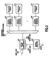
- an optical modulation apparatus with a configuration as shown in FIG. 2 is proposed which includes a wavelength multi-demultiplexer 207, one or more optical intensity modulators 209, and reflecting mirrors 211 equal to the optical intensity modulators in the number (see, Japanese patent application Laid-open No. 2002-318374 ).
- the multi-wavelength light which is input to an input port 203 of an optical input section 201, passes through an input/output port 205, and undergoes wavelength demultiplexing by a wavelength demultiplexer 207, modulating by individual optical intensity modulators 209, and reflection by optical reflectors 211. Then, the reflected light rays return the paths they have come with being multiplexed again by the wavelength multiplexer 207 and output from an output port 213 of the input/output means 201.
- the system configuration includes only one wavelength multi-demultiplexer 207. Consequently, it can facilitate the matching of the transmission central wavelengths of the wavelength multi-demultiplexer, and reduce the cost of the system.
- the individual wavelengths have their optical power reduced by the losses of optical devices used by the wavelength multi-demultiplexer and the like.
- the losses of fiber transmission paths linking them become nonnegligible. Since the reduction in the WDM signal power deteriorates the signal-to-noise ratio (SNR), the power must be amplified using an optical amplifier designated by the reference numeral 109 of FIG. 1 or by 215 of FIG. 2 .
- FIGs . 1 and 2 each show an example which amplifies the WDM signal power at once with a broadband optical amplifier that covers the entire wavelength band of the multi-wavelength light (see, Japanese patent application laid-open No. 2003-18853 ).
- the example employs a polarization independent optical amplifier that amplifies the optical intensity without depending on the polarization of the modulated light passing through the wavelength division multiplexing.
- Such an optical amplifier generally employs a fiber amplifier such as an erbium (Er) doped fiber amplifier (EDFA).
- Er erbium
- EDFA is an optical amplifier that amplifies the light traveling through the fiber by doping the core of the silica glass fiber with erbium ions Er 3+ , and by utilizing the stimulated emission in the transition proper to the ions.
- the SOA is an optical amplifier that amplifies the light traveling through the active layer of the semiconductor by the stimulated emission by reducing the reflectance of end faces of the cavity of the semiconductor laser.
- both types of the optical amplifiers have a broad gain bandwidth of 30 nm or more, they differ greatly in the lifetime of carriers in the excited level.
- the EDFA has the gain broadening established by the transition from a plurality of discrete excitation energy levels , it has a long carrier lifetime of an order of milliseconds, and uneven gain broadening.
- the SOA has a short carrier lifetime of an order of nanoseconds, and the gain broadening can be considered as uniform.
- the optical amplifier operates in the saturation region of the gain to obtain large output.
- the optical amplifier with the uniform gain broadening amplifies a plurality of different signal wavelengths in the saturation region of the gain, the individual wavelengths scramble for the gain, which causes crosstalk between the channels and degrades the signal waveform.
- fiber amplifiers such as the EDFA are usually used to amplify the WDM signal collectively as described above.
- the SOA is far economical from the viewpoint of the number of components.
- the SOA is more suitable for amplifying a single signal wavelength.
- the SOA has the following advantages.
- FIG. 3 shows as a conventional example 1 a configuration of a conventional optical modulation apparatus applicable to the optical intensity modulator 105 as shown in FIG. 1 .
- the system of the conventional example 1 is drawn assuming that an SOA is used as a modulator 306, and an optical modulation apparatus 303 is placed at a distance from a light source.
- the SOA modulator 306 has its one end coupled to an input transmission path 301 to which an optical signal is input and other end coupled to an output transmission path 309 from which the optical signal is output.
- the input/output transmission paths include optical connectors and splices in addition to a variety of optical devices such as an optical filter and optical coupler not shown.
- a wavelength multi-demultiplexer is inserted between the input/output transmission path 301 and the SOA modulator 306. These components all constitute reflection points. Since the reflection points are present at both end sides of the SOA optical amplifying section 306, the reflection points and the SOA constitute an optical cavity, which can make the operation of the SOA unstable. To prevent the defect, optical isolators 305 and 307, which allow the light to be transmitted in one direction, are inserted into both sides of the SOA as shown in FIG. 3 .
- FIG. 4 shows as a conventional example 2 a configuration of a conventional optical modulation apparatus applicable to the optical modulation circuit of FIG. 2 .
- FIG. 4 shows configurations of two types of optical modulation apparatuses 405 and 407.
- a first type optical modulation apparatus 405 is configured such that a bidirectional optical amplifier 409 amplifies the optical power of a continuous wave demultiplexed by a wavelength multi-demultiplexer 403, and an optical intensity modulator 411 receiving the continuous wave carries out intensity modulation by a data signal to generate modulated light followed to be reflected by an optical reflector 413, and that the reflected light passes through the optical intensity modulator 411 and bidirectional optical amplifier 409 once again.
- a second type optical modulation apparatus 407 is configured such that a bidirectional optical amplifier 415 amplifies the optical power of the continuous wave demultiplexed by the wavelength multi-demultiplexer 403, an optical loop constructed by using an optical circulator 417 receives the continuous wave, and an optical intensity modulator 419 installed in the optical loop carries out the intensity modulation by the data signal to generate modulated light, and that the modulated light passes through the optical circulator 417 and the bidirectional optical amplifier 415 once again.
- the optical reflector 413 can be a discrete component separated from the optical intensity modulator 411, or can be affixed to the end face of the optical intensity modulator 411 as an integrated combination thereof.
- an SOA is suitable because it is enough for these amplifiers to perform single wavelength amplification.
- Using the SOA as the bidirectional optical amplifiers 409 and 415 brings about signal degradation because of the gain scrambling between the continuous wave and modulated light in the saturation region of the gain.
- the continuous wave is modulated by the signal pattern of the modulated light within the optical amplifiers 409 and 415.
- the bidirectional optical amplifiers 409 and 415 be used in an unsaturated region in which when the sum of the output powers (or of the input powers) of the continuous wave and modulated light from the bidirectional optical amplifiers 409 and 415 is less than certain output power (or input power), the gain is kept constant.
- the configuration of the conventional example 1 as shown in FIG. 3 has a remaining problem of the end face reflection of the SOA device itself even if the optical isolators 305 and 307 are inserted into both ends of the SOA 306.
- the SOA 306 has its end faces applied with antireflection coating to reduce the end face reflectance, and the end face reflectance is usually smaller than the reflectance of the transmission path reflection.
- the SOA 306 has a large gain, the cavity effect of the optical modulation apparatus 303 increases, thereby making the amplifying operation unstable.
- the value of the end face reflectance imposes a limit on the gain permitted for the SOA. Accordingly, to achieve the high gain amplification by the SOA, it is necessary to connect SOAs in cascade as shown in FIG. 6 , for example.
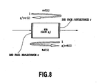
- the configuration of the conventional example 2 as shown in FIG. 4 it has reflected light 1 and reflected light 2 at the ends of the bidirectional optical amplifiers (SOA) 409 and 415.
- SOA bidirectional optical amplifiers
- the reflected light is large because of the amplification of the power of the reflected light before and after the end face reflection.
- the reflected light interferes with signal light, and brings about noise.
- the reflected light 1 and reflected light 2 will be explained later in the description of FIG. 8 .
- Document EP 1 267 510 discloses an optical demultiplexer including a wavelength-group demultiplexer (31) that demultiplexes multi-wavelength light into wavelength groups formed from wavelength channels, and channel demultiplexers (32-1 to 32-m) that demultiplex each wavelength group into wavelength channels light, and an optical multiplexer including channel multiplexers (34-1 to 34-m) that multiplex modulated signal light of each wavelength channel for each wavelength group, and a wavelength-group multiplexer (35) that multiplexes, for each wavelength group, WDM signal light output from the channel multiplexers.
- Document US 5,657,148 discloses a single-port, reflective, optical modulator with internal amplification including a semiconductor waveguide amplifier with a high reflector at one end.
- the present invention is implemented to solve the foregoing problems. Therefore it is an object of the present invention to provide an economical optical modulation apparatus that can reduce the effect of the reflected light rays and achieve the stable amplifying function by the device specification design and device configuration considering the effect of the reflection passing through the optical amplifiers in the optical modulation apparatus with a configuration including optical amplifiers connected in a multi-stage fashion, or in the optical modulation apparatus including optical amplifiers as bidirectional optical amplifiers.
- a first aspect of the present invention implements a stable amplifying function by reducing the effect of reflected light rays from end faces of a bidirectional optical amplifier by imposing a numerical limitation on the relationship between the gain of the bidirectional optical amplifier and the loss of the optical modulator in a reflection type optical modulator including the bidirectional optical amplifier, or in a multi-wavelength collective optical modulation apparatus combining the multiple optical modulators. It is provided an optical modulation apparatus according to claim 1. Further details are set out in the dependent claims.
- a bididrectional amplifier implements a stable amplifying function by reducing the effect of reflected light rays from end faces of a bidirectional optical amplifier by inserting a polarization rotation means into a reflection type optical modulator including the bidirectional optical amplifier, or into a multi-wavelength collective optical modulation apparatus combining the multiple optical modulators.
- a system implements both stable amplifying function and cost reduction by reducing the effect of reflected light rays by interposing optical isolators at every alternate SOAs in a transmission-type optical modulation apparatus including semiconductor optical amplifiers (SOAs) connected in a multistage fashion.
- SOAs semiconductor optical amplifiers
- the first example has, in a transmission-type optical modulation apparatus including semiconductor optical amplifiers (SOAs) connected in cascade, optical isolators inserted at every alternate units to reduce the effect of the reflected light, thereby implementing the stable amplifying function and cost reduction at the same time.
- SOAs semiconductor optical amplifiers
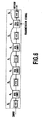
- FIG. 7 is a diagram illustrating reflected light rays when a plurality of SOAs are arranged in the multistage connection.
- the multistage connection to operate it as an optical modulation apparatus , one of the SOAs must be used as an optical intensity modulator, or an external modulator must be inserted.
- the SOAs are assumed to function just as an optical amplifier.
- the input/output transmission paths 301 and 309 constitute a reflection point.
- the SOAs (S 1 , S 2 , ⁇ , S i , ⁇ , S n ) have reflection ends at both ends of the devices themselves, the SOAs become reflection points by themselves.
- FIG. 8 is a diagram illustrating the reflected light rays of the SOA. Assume that the SOA has a gain g i , and end face reflectance r, then, when light with optical power 1 is input to the SOA, the SOA has reflection optical power of g i 2 r. This means that the end face reflectance is multiplied by g i 2 . The reflection can take place bidirectionally in every SOA.
- the reflections in the traveling direction of the signal light are designated by Ref(0), Ref(1), ⁇ , Ref(i), and Ref (n) in this order from the input-side, and the reflections in the opposite direction of the signal light are designated by ref(1), ref (2), ⁇ , ref(i), and ref(n+1) in this order from the input-side.
- the Ref(0) and ref(n+1) are input-side transmission path reflection and output-side transmission path reflection, respectively, and the remaining reflections Ref(i) and ref(i) represent bidirectional reflections of the semiconductor optical amplifier S 1 .
- the symbols Ref(0), Ref(1) and Ref(2) designate the reflections in the traveling direction of the signal light, and the symbols ref(1), ref(2) and ref(3) designate the reflections in the opposite direction.
- the Ref(0) and ref(3) designate the input-side transmission path reflection and output-side transmission path reflection, respectively, and Ref(1) and ref(1), and Ref (2) and ref (2) are the reflections of the semiconductor optical amplifiers S 1 and S 2 , respectively.
- the reflection becomes a problem because following the reflection (first reflection) in the direction opposite to the traveling direction of the signal light , the reflection (second reflection) in the traveling direction occurs, which will make the signal optical power unstable because of interference with the signal light.
- the SOAs since the SOAs have a gain, the reflected light rays are amplified by that gain, which enhances the effect.
- the ratios of the twice reflected light rays to the signal light are in the order of a square of the reflectance at the reflection point.
- the ratio of the twice reflected light rays to the signal light is increased by a square of the gain of the SOA passed through as compared with the order of the square of the reflectance at the reflection point.
- FIGs. 11A-11C are diagrams illustrating configurations of the optical modulation apparatus of the first example , into which optical isolators are inserted at every alternate optical path.
- O 1 and O 2 each designate an optical isolator.
- the first optical isolator O 1 is inserted into the first optical path x 1 between the input-side transmission path and the first SOA S 1
- the second optical isolators O 1 is inserted into the third optical path x 3 between the second SOA S 2 and third SOA S 3 .
- the present embodiment is characterized by inserting the optical isolators at every alternate optical path.
- the third SOAS 3 is used as the optical intensitymodulator in FIG. 11A
- the second SOA S 2 is used as the optical intensity modulator in FIG. 11B
- the first SOA S 1 is used as the optical intensity modulator in FIG. 11C .
- the configuration of the embodiment can implement the system that can compensate for the optical power loss on the transmission path and achieve the modulation operation simultaneously in the optical communication system having the light source for outputting the continuous wave and the optical intensity modulator, which are placed at a distance via the transmission path.
- FIGs. 12A-12C are diagrams each showing a configuration of the optical modulation apparatus of a second example .
- the present example is a variation of the first example, which has an optical intensity modulator M inserted between any two of three SOAs S 1 , S2 and S 3 constituting the optical amplifier.
- FIG. 12A shows a configuration having the optical intensity modulator M inserted in to a section in which neither the optical isolator O 1 nor O 2 is inserted.
- the example is shown here which has the optical intensity modulator M inserted into the second optical path (optical connection means) x 2 between the first and second SOAs S 1 and S 2
- the optical intensity modulator M can be inserted into a fourth optical path x 4 between the third SOAS 3 and the output terminal. In the latter case, however, it is necessary to use an optical intensity modulator M that can handle the optical power amplified by the final stage SOA S 3 .
- the intensity modulation is carried out twice by the optical intensity modulator M until the continuous wave output from the first SOA S 1 interferes with the twice reflected light ray of the continuous wave at the second SOA S 2 and first SOA S 1 . Accordingly, the ratio of the twice reflected light ray to the signal light is relatively small as compared with the case where no optical intensity modulator M is inserted.
- FIG. 12B shows a configuration that has the optical intensity modulator M inserted into the section into which the optical isolator O 2 is inserted.
- the example shown has the optical intensity modulator M inserted into the third optical path x 3 between the second and third SOAs S 2 and S 3
- the optical intensity modulator M can be inserted into the first optical path X 1 between the input terminal and the first SOA S 1 .
- the order of connection of the optical isolator O 2 and the optical intensity modulator M is arbitrary as shown in FIGs. 12B-12C .
- an electro absorption optical intensity modulator (EA modulator) can be used, for example. Since the foregoing first embodiment uses the SOA as the optical intensity modulator, it is difficult to carry out the modulation operation of the order of G (bps) or more. In contrast, the EA modulator used as the optical intensity modulator can handle the modulation operation of the order of 40G (bps).
- An embodiment of the optical modulation apparatus in accordance with the present invention relates to a system that can achieve the stable amplifying function by reducing the effect of the reflected light rays on the end faces of the bidirectional optical amplifiers by imposing the following numerical limitation on the gain of the amplifier in the foregoing system configuration including the bidirectional optical amplifiers as shown in FIG. 4 .
- the numerical limitation on the amplifier gain in accordance with the present invention will be described below.
- first reflected light 1 travels in the same direction as the modulated light
- second reflected light 2 travels in the same direction as the continuous wave.
- the continuous wave undergoes the intensity modulation and becomes the modulated light. Since the reflected light 2 travels through the same path as the continuous wave, the modulated light is finally provided with the reflected light 1 and reflected light 2.
- the modulated light interferes with the same polarization direction components of the reflected light 1 and reflected light 2, thereby generating intensity fluctuations as beat noise.
- the multiple reflection light rays which are reflected off the first end face of the bidirectional optical amplifier 409 or 415 and then reflected off the second end face thereof again, are assumed to be sufficiently small and are neglected.
- the mark-to-space ratio of the transmission signal is assumed to be 1/2. (Since the continuous mark or space in the data signal train makes it difficult to extract a clock signal at the reception of the signal, a technique of making the mark-to-space ratio nearly 1/2 is usually employed such as scramble in the SDH (synchronous digital hierarchy) or 8 B ⁇ 10 B (bel) conversion in the gigabit ether.)
- the input continuous wave power to the bidirectional optical amplifiers 409 and 415, the gain of the bidirectional optical amplifiers 409 and 415, the difference between the modulated light output power and the input continuous wave power to the optical intensity modulators 411 and 419 , and the reflectance of the entire bidirectional optical amplifier are 1, g, x and r', respectively, then the modulation optical power of the optical modulator output, the power of the reflected light 1, and the power of the reflected light 2 are represented by g 2 x, r' and g 2 x 2 r', respectively.
- the problem to be considered here is the interference between the modulated light and the reflected light, it is enough to consider only the effect of the reflected light when the modulated light is at the mark.
- the transmission signal has the mark-to-space ratio of 1/2
- the mark level power of the output modulated light of the optical modulator, and the mark level power of the ref lected light 2 are 2g 2 x and 4g 2 x 2 r', respectively.
- the probability is 1/2 that the modulated light and reflected light 2 are mark at the same time in the optical modulator output, the effect of the reflected light 2 is halved.
- S N 2 ⁇ g 2 ⁇ x g 2 ⁇ r + 2 ⁇ g 4 ⁇ x 2 ⁇ r
- mark-side optical electrical field of the modulated light is E 0 exp[ i ( ⁇ c t + ⁇ 0 )]
- mark-side optical electrical field of the reflected light 1 is E 1 exp[ i ( ⁇ c t+ ⁇ 1 )]
- mark-side optical electrical field of the reflected light 2 is E 2 exp[ i( ⁇ c t + ⁇ 2 )]
- the optical electrical field before reception is expressed by the following expression.
- E OUT t E 0 exp i ⁇ ⁇ c ⁇ t + ⁇ 0 + E 1 exp i ⁇ ⁇ c ⁇ t + ⁇ 1 + E 2 exp i ⁇ ⁇ c ⁇ t + ⁇ 2
- the received optical current is given by the following expression by neglecting all the coefficients required.
- i p E 0 2 + 2 ⁇ E 0 ⁇ E 1 exp i ⁇ ⁇ 0 - ⁇ 1 + 2 ⁇ E 0 ⁇ E 2 exp i ⁇ ⁇ 0 - ⁇ 2 + E 1 2 + E 2 2 + 2 ⁇ E 1 ⁇ E 2 exp i ⁇ ⁇ 1 - ⁇ 2
- the first term is the modulated light itself, and the second and subsequent terms are noise.
- the first term to sixth term represent when the modulated light and reflected light are all on the mark-side: the modulation optical power; the beat (interference) between the modulated light and the reflected light 1; the beat (interference) between the modulated light and the reflected light 2; the power of the reflected light 1; the power of the reflected light 2; and the beat (interference) between the reflected light 1 and the reflected light 2.
- the fourth to sixth terms are negligible because the reflected light is small as compared with the modulated light.
- normalized beat noise power is defined as follows.
- ⁇ RIN 2 2 ⁇ E 0 2 ⁇ E 1 2 + E 0 2 ⁇ E 2 2 E 0 2 2
- the beat noise when a plurality of reflection points are involved can be handled as Gaussian distribution with a variance given by expression (7). On the contrary, when the number of the reflection points is small, excessive estimation of the beat noise is made.
- the reflected light rays the reflected light 1 and reflected light 2 from both end faces of the bidirectional optical amplifiers 409 and 415.
- the bidirectional optical amplifiers 409 and 415 there are input/output terminal reflections of a variety of optical devices inserted into the system, and reflections by optical connectors, and the reflected light rays from these reflection points undergo the gains of the bidirectional optical amplifiers 409 and 415, and become nonnegligible depending on their reflectances.
- FIG. 13 shows calculation results using the foregoing expression (8).
- the horizontal axis represents a modulation section loss (L) [dB]
- the vertical axis represents a Q value [dB] on the left side
- the optical modulation apparatus gain [dB] on the right side.
- the Q value here refers to an evaluation parameter that determines the signal-to-noise ratio (SNR) of the modulated light proposed in IEEE Photon. Technol. Lett.
- SNR signal-to-noise ratio
- the modulation section loss that takes the maximum Q value is the modulation section loss that takes the maximum Q value.
- the region ( ⁇ ) it is as described above.
- the upper limit values of L in the regions ( ⁇ ) and ( ⁇ ) indicate that the optical modulation gain is equal to or greater than 0 [dB].
- the modulation section loss L itsvalueislogically determined from the fact that the Q value curve has the left-right symmetry as described above.
- the range of L is independent of the value G.
- solving the quadratic equation for x which is obtained by substituting the value x defined in the foregoing expression (3) into the foregoing expression (1), and by making the half of that result (3 dB reduction) equal to expression (1), gives the following solution.
- x 2 ⁇ 2 ⁇ 6 2 ⁇ g
- the optical modulation apparatus can keep the ratio low of the reflected light to the modulated light with placing the modulation section loss L in a given range in the region ( ⁇ ) (such as ( ⁇ ), ( ⁇ ) and ( ⁇ )).
- FIG. 14 shows a configuration of the optical modulation apparatus of a third example.
- the optical modulation apparatus of the present example implements a stable amplifying function by reducing the effect of the reflected light from the end faces of the bidirectional optical amplifiers by inserting polarization rotation means.
- the present system is a multi-wavelength collective optical modulation apparatus that includes a polarization demultiplexer 501 for separating the input multi-wavelength light from the output modulated light by the difference in the plane of polarization; a wave length multi-demultiplexer 502 for demultiplexing the multi-wavelength light into every predetermined wavelengths; bidirectional optical amplifiers 503 for bidirectionally amplifying the individual single wavelength optical powers demultiplexed; polarization rotation means 504 each for bidirectionally rotating the plane of polarization of the single wavelength light; optical intensity modulators 505 each for bidirectionally modulating the intensity of the single wavelength light; and optical reflectors 506 for feeding the modulated single wavelength light rays output from the optical intensity modulators 505 back to the bidirectional optical amplifiers 503.
- a polarization demultiplexer 501 for separating the input multi-wavelength light from the output modulated light by the difference in the plane of polarization
- a wave length multi-demultiplexer 502 for demultiplexing the multi
- polarization demultiplexer 501 a polarization beam splitter (PBS) is applicable.
- PBS polarization beam splitter
- a configuration is also possible which has the wavelength multi-demultiplexer 502 produce output light via an optical circulator or an optical coupler, and extracts the light whose polarization shifts from that of the input light by 90 degrees by using a polarizer.
- an AWG is applicable, for example.
- the AWG has the light incident onto an input waveguide output from a different output waveguide in accordance with the wavelength.
- the AWG has reversibility, and can multiplex a plurality of wavelength light rays into a single output waveguide.
- the bidirectional optical amplifiers 503, SOAs can be used, for example.
- the SOA is an optical amplifier for amplifying the light traveling through the active layer in the semiconductor by stimulated emission by reducing the reflection from the cavity end faces of a semiconductor laser.
- fiber amplifiers such as erbium doped fiber amplifiers (EDFAs) can also be used.
- EDFAs erbium doped fiber amplifiers
- the fiber amplifier is composed of a semiconductor laser for outputting pumping light, a doped fiber doped with erbium and the like, and a coupler for coupling the pumping light to the doped fiber, it will be more expensive than the SOA from the viewpoint of the number of the components. Accordingly, the SOA has a cost advantage.
- the polarization rotation means 504 is installed between the bidirectional optical amplifiers 503 and the optical intensity modulators 505.
- a quarter-wave plate or a Faraday cell is applicable.
- a Faraday mirror is usable which attaches a reflecting mirror to an output end of the Faraday cell.
- optical intensity modulators 505 a Mach Zehnder type optical intensitymodulator or an electro absorption optical intensity modulator (EA modulator) is applicable, for example. They have a function of carrying out intensity modulation of the single wavelength light by a data signal. These optical intensity modulators can achieve the intensity modulation by a 40 G(bps) order modulation signal at a practical level.
- EA modulator electro absorption optical intensity modulator
- a mirror having metal coating or dielectric multi-layer coating is applicable, for example.
- a diffraction grating or fiber Bragg grating is also applicable to the optical reflector.
- an optical reflector can be used inwhich a diffraction grating is directlywritten on an optical waveguide.
- One of the output ports of the polarization demultiplexer 501 is optically connected to the input waveguide of the wavelength multi-demultiplexer 502 via a spatial optical system or an optical waveguide.
- the output waveguides of the wavelength multi-demultiplexer 502 are optically connected to first ports of the bidirectional optical amplifiers 503 via a spatial optical system or optical waveguides.
- Second ports of the bidirectional optical amplifiers 503 are optically connected to first ports of the polarization rotation means 504 via a spatial optical system or optical waveguides as well.
- Second ports of the polarization rotation means 504 are optically connected to first ports of the optical intensity modulators 505 via a spatial optical system or optical waveguides as well.
- Second ports of the optical intensity modulators 505 are optically connected to the optical reflectors 507 via a spatial optical system or optical waveguides as well.
- the polarization demultiplexer 501 separates the inputs to the optical intensity modulators 505 from their modulated light outputs.
- the angles of the planes of polarization of the input light rays and the output light rays differ by 90 degrees. Accordingly, the input light rays can be separated from the output light rays by extracting the particular polarized waves from the output light rays by the polarization demultiplexer 501.
- the multi-wavelength light input to the wavelength multi-demultiplexer 502 via the input waveguide is demultiplexed to the individual wavelengths by the wave length multi-demultiplexer 502.
- Each single wavelength light passing through the demultiplexing is led to corresponding one of the bidirectional optical amplifiers 503 to have its power amplified.
- the bidirectional optical amplifiers 503 bring about signal degradation because of the gain scrambling between the continuous waves and modulated light rays in the saturation region of the gain. Accordingly, as illustrated in FIG. 5 , it is preferable that the bidirectional optical amplifiers 503 be used in the unsaturated region of the gain in which the gain (the vertical axis) is maintained at a constant value as long as the sum of the output powers (the horizontal axis) (or the sum of input powers) of the continuous waves and the modulated light from the bidirectional optical amplifiers 503 is equal to or less than a particular output power (or input power).
- the continuous waves (single wavelength light rays) whose powers are amplified by the individual bidirectional optical amplifiers 503 are input to the corresponding polarization rotation means 504.
- the polarization rotation means 504 rotate the planes of polarization of the continuous waves by 45 degrees, and supply them to the optical intensity modulators 505.
- the optical intensity modulators 505 carry out the intensity modulation of the continuous waves by modulation signals (data signals).
- the modulated single wavelength light rays are output from the optical reflector side ports of the optical intensity modulators 505, and are input to the optical reflectors 507.
- the modulated light rays reflected by the optical reflectors 507 pass through the optical intensity modulators 505 again, and are input to the polarization rotation means 504.
- the modulated light rays have their planes of polarization rotated by 45 degrees by the polarization rotation means 504, and are input to the bidirectional optical amplifiers 503 which amplify the optical powers again. Since the output modulated light rays of the bidirectional optical amplifiers 503 have the planes of polarization different by 90 degrees from those of the input light rays, the polarization demultiplexer 501 can separate the output light rays from the input light rays. Accordingly, the output modulated light rays from the bidirectional optical amplifiers 503 are multiplexed by the wavelength multi-demultiplexer 502, and are output from the output port of the polarization demultiplexer 501 to a system outside.
- the optical amplifier cannot include an optical isolator. Accordingly, it is necessary to consider the effect of the end face reflections from both terminals of the optical amplifying paths.
- FIG. 4 there are two reflected light rays in the bidirectional transmission (reflected light ray 1 and reflected light ray 2).
- the reflected light ray 1 propagates in the same direction as the modulated light, and the reflected light ray 2 in the same direction as the continuous waves.
- the continuous waves undergo the intensity modulation and become modulated light, and the reflected light ray 2 travels through the same path as the continuous waves.
- the modulated light rays are provided with the reflected light ray 1 and reflected light ray 2.
- the modulated light rays interfere with the same polarization direction components of the reflected light ray 1 and reflected light ray 2, causing the intensity fluctuations as the beat noise.
- the reflected light ray 1 and reflected light ray 2 from the bidirectional optical amplifiers 503 are orthogonal to the polarization direction of the continuous waves or modulated light rays traveling in the same direction as indicated by arrows enclosed by circles representing the directions of the planes of polarization in FIG. 15 . Since the reflected light ray 1 and the modulated light rays have the polarization directions orthogonal to each other, the polarization demultiplexer 501 can separate them at the output.
- the reflected light ray 2 has the polarization direction orthogonal to that of the continuous waves, and maintain the polarization relationship after the reflected light ray 2 passes through the intensity modulation and become modulated light rays.
- the reflected light ray 2 can be separated from the continuous waves so as to output by the polarization demultiplexer 501 in the same manner as the reflected light ray 1.
- the intensity fluctuations due to the interference between the two light rays can be eliminated.
- the planes of polarization of the light rays are the same in the two directions on the paths from the outputs of the polarization rotation means 504 to the return to the polarization rotation means 504 after the reflection by the optical reflectors 507. Consequently, it is possible to use as the optical intensity modulators 505 an optical intensity modulator such as LiNbO 3 Mach Zehnder type optical intensity modulator capable of carrying out modulation only for a single input polarized wave.
- an optical intensity modulator such as LiNbO 3 Mach Zehnder type optical intensity modulator capable of carrying out modulation only for a single input polarized wave.
- FIG. 16 shows a configuration of the optical modulation apparatus of a fourth example.
- the system of the fourth example has polarizers 506, which enable only single polarized waves to pass through, interposed before or after the optical intensity modulators 505 of the multi-wavelength collective optical modulation apparatus in the foregoing fourth embodiment (inFIG. 16, they are interposed after). Since the remaining configuration is the same as that of the third example, the detailed description thereof is omitted here.
- the polarization extinction ratio between two orthogonal polarized waves deteriorates markedly when coupling a plurality of optical devices and fibers.
- the polarizers 506 can be inserted into the optical paths. The insertion of the polarizers 506 can recover the polarization extinction ratio degraded.
Abstract
Description
- The present invention relates to an optical modulation apparatus used for optical communication, and particularly to a constructing technique of the optical modulation apparatus constructed by combining an optical amplifier such as a semiconductor optical amplifier with an optical intensity modulator.
- Conventionally, systems have been studied which apply multi-wavelength light including a plurality of optical carriers generated by an optical short-pulse laser or by amplitude modulation/phasemodulation to wavelength division multiplexing (WDM) signal transmission. Such multi-wavelength light has the same spectral spacing between individual side modes so that the channels obtained by wavelength demultiplexing of the side modes have the same wavelength spacing. Accordingly, such multi-wavelength light is simpler in wavelength constellation than multi-wavelength light based on a method of preparing separate lasers for individual channels and setting wavelengths for the individual channels.
- To implement a WDM signal transmission system using the multi-wavelength light, one of the important problems is the simplification of the configuration of an optical modulation circuit and its economization.
FIG. 1 shows a configuration of a conventional optical modulation circuit. The multi-wavelength light generated by amulti-wavelength light source 101 undergoes wavelength demultiplexing by awavelength demultiplexer 103, modulatinig by individualoptical intensity modulators 105, and multiplexing by awavelength multiplexer 107 again. The configuration as shown inFIG. 1 requires two wavelength multi-demultiplexers 103 and 107 having the same absolute value in the transmission central wavelengths. Thus, an optical modulation apparatus with a configuration as shown inFIG. 2 is proposed which includes a wavelength multi-demultiplexer 207, one or moreoptical intensity modulators 209, and reflectingmirrors 211 equal to the optical intensity modulators in the number (see, Japanese patent application Laid-open No.2002-318374 - In the optical modulation apparatus as shown in
FIG. 2 , the multi-wavelength light, which is input to aninput port 203 of anoptical input section 201, passes through an input/output port 205, and undergoes wavelength demultiplexing by awavelength demultiplexer 207, modulating by individualoptical intensity modulators 209, and reflection byoptical reflectors 211. Then, the reflected light rays return the paths they have come with being multiplexed again by thewavelength multiplexer 207 and output from anoutput port 213 of the input/output means 201. According to the system configuration, it includes only one wavelength multi-demultiplexer 207. Consequently, it can facilitate the matching of the transmission central wavelengths of the wavelength multi-demultiplexer, and reduce the cost of the system. - In either
FIG. 1 orFIG. 2 , the individual wavelengths have their optical power reduced by the losses of optical devices used by the wavelength multi-demultiplexer and the like. In addition, as for the system having the multi-wavelength light source and the optical modulators placed at a distance physically, the losses of fiber transmission paths linking them become nonnegligible. Since the reduction in the WDM signal power deteriorates the signal-to-noise ratio (SNR), the power must be amplified using an optical amplifier designated by thereference numeral 109 ofFIG. 1 or by 215 ofFIG. 2 . -
FIGs . 1 and2 each show an example which amplifies the WDM signal power at once with a broadband optical amplifier that covers the entire wavelength band of the multi-wavelength light (see, Japanese patent application laid-open No.2003-18853 - Although both types of the optical amplifiers have a broad gain bandwidth of 30 nm or more, they differ greatly in the lifetime of carriers in the excited level. Since the EDFA has the gain broadening established by the transition from a plurality of discrete excitation energy levels , it has a long carrier lifetime of an order of milliseconds, and uneven gain broadening. In contrast with this, the SOA has a short carrier lifetime of an order of nanoseconds, and the gain broadening can be considered as uniform. Generally, the optical amplifier operates in the saturation region of the gain to obtain large output. When the optical amplifier with the uniform gain broadening amplifies a plurality of different signal wavelengths in the saturation region of the gain, the individual wavelengths scramble for the gain, which causes crosstalk between the channels and degrades the signal waveform. Accordingly, fiber amplifiers such as the EDFA are usually used to amplify the WDM signal collectively as described above. However, comparing the SOA that excites the semiconductor by injection current with the EDFA that includes a semiconductor laser for outputting pumping light, a doped fiber doped with erbium or the like, and a coupler for coupling the pumping light to the doped fiber, the SOA is far economical from the viewpoint of the number of components. In particular, the SOA is more suitable for amplifying a single signal wavelength.
- To amplify the WDM signal collectively using the fiber amplifier, it is essential to increase the power of the optical amplifier to compensate for the optical losses caused by optical components such as the wavelength multi-demultiplexer and optical intensity modulators. However, a broadband, high-power light amplifier covering the entire wavelength band of the multi-wavelength light is very expensive even if used alone. Accordingly, depending on the wavelength bandwidth and output required, a configuration that amplifies the wavelengths individually by the SOAs can sometimes implement the optical modulation circuit more cheaply than the configuration using the fiber amplifier.
- In addition, the SOA has the following advantages.
- The SOA is applicable as a modulator by varying the injection current in response to a modulation signal.
- The SQA can be integrated with an electro absorption modulator (EA modulator) and the like
- Next, typical configuration examples of the optical modulation apparatus using the SOAs will be described.
-
FIG. 3 shows as a conventional example 1 a configuration of a conventional optical modulation apparatus applicable to theoptical intensity modulator 105 as shown inFIG. 1 . The system of the conventional example 1 is drawn assuming that an SOA is used as amodulator 306, and anoptical modulation apparatus 303 is placed at a distance from a light source. TheSOA modulator 306 has its one end coupled to aninput transmission path 301 to which an optical signal is input and other end coupled to anoutput transmission path 309 from which the optical signal is output. The input/output transmission paths, however, include optical connectors and splices in addition to a variety of optical devices such as an optical filter and optical coupler not shown. Furthermore, although omitted from this figure, a wavelength multi-demultiplexer is inserted between the input/output transmission path 301 and theSOA modulator 306. These components all constitute reflection points. Since the reflection points are present at both end sides of the SOA optical amplifyingsection 306, the reflection points and the SOA constitute an optical cavity, which can make the operation of the SOA unstable. To prevent the defect,optical isolators FIG. 3 . -
FIG. 4 shows as a conventional example 2 a configuration of a conventional optical modulation apparatus applicable to the optical modulation circuit ofFIG. 2 .FIG. 4 shows configurations of two types ofoptical modulation apparatuses optical modulation apparatus 405 is configured such that a bidirectionaloptical amplifier 409 amplifies the optical power of a continuous wave demultiplexed by a wavelength multi-demultiplexer 403, and anoptical intensity modulator 411 receiving the continuous wave carries out intensity modulation by a data signal to generate modulated light followed to be reflected by anoptical reflector 413, and that the reflected light passes through theoptical intensity modulator 411 and bidirectionaloptical amplifier 409 once again. A second typeoptical modulation apparatus 407 is configured such that a bidirectional optical amplifier 415 amplifies the optical power of the continuous wave demultiplexed by the wavelength multi-demultiplexer 403, an optical loop constructed by using anoptical circulator 417 receives the continuous wave, and anoptical intensity modulator 419 installed in the optical loop carries out the intensity modulation by the data signal to generate modulated light, and that the modulated light passes through theoptical circulator 417 and the bidirectional optical amplifier 415 once again. In the formeroptical modulation apparatus 405, theoptical reflector 413 can be a discrete component separated from theoptical intensity modulator 411, or can be affixed to the end face of theoptical intensity modulator 411 as an integrated combination thereof. - As the
bidirectional amplifiers 409 and 415 used in the configuration ofFIG. 4 , an SOA is suitable because it is enough for these amplifiers to perform single wavelength amplification. Using the SOA as the bidirectionaloptical amplifiers 409 and 415, however, brings about signal degradation because of the gain scrambling between the continuous wave and modulated light in the saturation region of the gain. Specifically, the continuous wave is modulated by the signal pattern of the modulated light within theoptical amplifiers 409 and 415. - Therefore it is preferable as illustrated in
FIG. 5 that the bidirectionaloptical amplifiers 409 and 415 be used in an unsaturated region in which when the sum of the output powers (or of the input powers) of the continuous wave and modulated light from the bidirectionaloptical amplifiers 409 and 415 is less than certain output power (or input power), the gain is kept constant. - The configuration of the conventional example 1 as shown in
FIG. 3 has a remaining problem of the end face reflection of the SOA device itself even if theoptical isolators SOA 306. Generally, the SOA 306 has its end faces applied with antireflection coating to reduce the end face reflectance, and the end face reflectance is usually smaller than the reflectance of the transmission path reflection. However, when the SOA 306 has a large gain, the cavity effect of theoptical modulation apparatus 303 increases, thereby making the amplifying operation unstable. In other words, the value of the end face reflectance imposes a limit on the gain permitted for the SOA. Accordingly, to achieve the high gain amplification by the SOA, it is necessary to connect SOAs in cascade as shown inFIG. 6 , for example. - As a multi-stage configuration of the SOAs, a two-stage cascade configuration of SOA +EA modulators (which will be described later) is proposed (Relevant Reference 1: Ohman, F.; Bischoff, S. ; Tromborg, B.; Mork, J.; "Noise properties and cascadability of SOA-EA regenerators", Lasers and Electro-Optics Society, 2002. LEOS 2002. The 15th Annual Meeting of the IEEE, ). To minimize the effect of the optical reflection in the multi-stage configuration of the SOAs, although it is possible to insert optical isolators into the input/output ends of all the multi-stage SOAs as shown in
FIG. 6 , it is not desirable from the viewpoint of cost. In addition, theRelevant Reference 1 describes nothing about the insertion of the optical isolators. - As for the configuration of the conventional example 2 as shown in
FIG. 4 , it has reflectedlight 1 and reflectedlight 2 at the ends of the bidirectional optical amplifiers (SOA) 409 and 415. Even though the end faces of bidirectionaloptical amplifiers 409 and 415 are made to have low reflectance by the antireflection coating, the reflected light is large because of the amplification of the power of the reflected light before and after the end face reflection. Thus, the reflected light interferes with signal light, and brings about noise. Incidentally, the reflectedlight 1 and reflectedlight 2 will be explained later in the description ofFIG. 8 . -
Document EP 1 267 510 discloses an optical demultiplexer including a wavelength-group demultiplexer (31) that demultiplexes multi-wavelength light into wavelength groups formed from wavelength channels, and channel demultiplexers (32-1 to 32-m) that demultiplex each wavelength group into wavelength channels light, and an optical multiplexer including channel multiplexers (34-1 to 34-m) that multiplex modulated signal light of each wavelength channel for each wavelength group, and a wavelength-group multiplexer (35) that multiplexes, for each wavelength group, WDM signal light output from the channel multiplexers. - Document
US 5,657,148 discloses a single-port, reflective, optical modulator with internal amplification including a semiconductor waveguide amplifier with a high reflector at one end. - S. Borella et al. disclose in Proceedings of the IEEE, Vol. 85, No. 8, (1997), pages 1274-1307, optical devices in WDM networks.
- The present invention is implemented to solve the foregoing problems. Therefore it is an object of the present invention to provide an economical optical modulation apparatus that can reduce the effect of the reflected light rays and achieve the stable amplifying function by the device specification design and device configuration considering the effect of the reflection passing through the optical amplifiers in the optical modulation apparatus with a configuration including optical amplifiers connected in a multi-stage fashion, or in the optical modulation apparatus including optical amplifiers as bidirectional optical amplifiers.
- A first aspect of the present invention implements a stable amplifying function by reducing the effect of reflected light rays from end faces of a bidirectional optical amplifier by imposing a numerical limitation on the relationship between the gain of the bidirectional optical amplifier and the loss of the optical modulator in a reflection type optical modulator including the bidirectional optical amplifier, or in a multi-wavelength collective optical modulation apparatus combining the multiple optical modulators. It is provided an optical modulation apparatus according to
claim 1. Further details are set out in the dependent claims. - A bididrectional amplifier implements a stable amplifying function by reducing the effect of reflected light rays from end faces of a bidirectional optical amplifier by inserting a polarization rotation means into a reflection type optical modulator including the bidirectional optical amplifier, or into a multi-wavelength collective optical modulation apparatus combining the multiple optical modulators.
- A system implements both stable amplifying function and cost reduction by reducing the effect of reflected light rays by interposing optical isolators at every alternate SOAs in a transmission-type optical modulation apparatus including semiconductor optical amplifiers (SOAs) connected in a multistage fashion.
-
-
FIG. 1 is a block diagram showing a configuration of a conventional optical modulation circuit; -
FIG. 2 is a block diagram showing a configuration of a conventional reflection type optical modulation apparatus; -
FIG. 3 is ablock diagram showing a configuration of a conventional optical modulation apparatus utilizing a semiconductor optical amplifier; -
FIG. 4 is a block diagram showing a configuration of a conventional optical modulation apparatus utilizing bidirectional optical amplifiers; -
FIG. 5 is a graph illustrating an unsaturated region of a semiconductor optical amplifier; -
FIG. 6 is a block diagram showing a configuration conceivable as an optical modulation apparatus that can achieve high gain amplification by multistage connection of semiconductor optical amplifiers; -
FIG. 7 is a schematic diagram illustrating behavior of reflected light rays in a multistage connection of a plurality of semiconductor optical amplifiers; -
FIG. 8 is a schematic diagram illustrating reflected light rays of a semiconductor optical amplifier; -
FIG. 9 is a schematic diagram illustrating the behavior of reflected light rays in a multistage connection of two semiconductor optical amplifiers; -
FIG. 10 is a table illustrating ratios of the reflected light rays to signal light inFIG. 9 ; -
FIGs. 11A-11C are block diagrams each showing a configuration of an optical modulation apparatus of a first example -
FIGs. 12A-12C are block diagrams each showing a configuration of an optical modulation apparatus of a second example; -
FIG. 13 is a graph illustrating characteristics of an optical modulation apparatus of an embodiment in accordance with the present invention; -
FIG. 14 is a block diagram showing a configuration of an optical modulation apparatus of a third example; -
FIG. 15 is a schematic diagram illustrating directions of planes of polarization in the third example; and -
FIG. 16 is a block diagram showing a configuration of an optical modulation apparatus of a fourth example. - The best mode for carrying out the invention will now be described with reference to the accompanying drawings.
- The first example has, in a transmission-type optical modulation apparatus including semiconductor optical amplifiers (SOAs) connected in cascade, optical isolators inserted at every alternate units to reduce the effect of the reflected light, thereby implementing the stable amplifying function and cost reduction at the same time. Before describing concrete configuration examples of the present example, its principle will be explained.
-
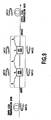
FIG. 7 is a diagram illustrating reflected light rays when a plurality of SOAs are arranged in the multistage connection. In the multistage connection , to operate it as an optical modulation apparatus , one of the SOAs must be used as an optical intensity modulator, or an external modulator must be inserted. However, to simplify the description of the reflected light rays here, the SOAs are assumed to function just as an optical amplifier. - In
FIG. 7 , n (>= 2) semiconductor optical amplifiers (S1, S2, ··, Si, ··, Sn) are coupled in series via n+1 optical paths (x1, x2, ··, xi, ··, xn+1) inclusive of input/output paths which are connected to an input-side transmission path 301 and an output-side transmission path 309, respectively. As described above, the input/output transmission paths -
FIG. 8 is a diagram illustrating the reflected light rays of the SOA. Assume that the SOA has a gain gi, and end face reflectance r, then, when light withoptical power 1 is input to the SOA, the SOA has reflection optical power of gi 2r. This means that the end face reflectance is multiplied by gi 2. The reflection can take place bidirectionally in every SOA. - In
FIG. 7 , the reflections in the traveling direction of the signal light are designated by Ref(0), Ref(1), ··, Ref(i), and Ref (n) in this order from the input-side, and the reflections in the opposite direction of the signal light are designated by ref(1), ref (2), ··, ref(i), and ref(n+1) in this order from the input-side. The Ref(0) and ref(n+1) are input-side transmission path reflection and output-side transmission path reflection, respectively, and the remaining reflections Ref(i) and ref(i) represent bidirectional reflections of the semiconductor optical amplifier S1. - The effect of the reflected light rays will be considered in the case of n = 2 for simplicity.
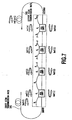
FIG. 9 is a diagram illustrating the reflected light rays when n = 2. The symbols Ref(0), Ref(1) and Ref(2) designate the reflections in the traveling direction of the signal light, and the symbols ref(1), ref(2) and ref(3) designate the reflections in the opposite direction. The Ref(0) and ref(3) designate the input-side transmission path reflection and output-side transmission path reflection, respectively, and Ref(1) and ref(1), and Ref (2) and ref (2) are the reflections of the semiconductor optical amplifiers S1 and S2, respectively. The reflection becomes a problem because following the reflection (first reflection) in the direction opposite to the traveling direction of the signal light , the reflection (second reflection) in the traveling direction occurs, which will make the signal optical power unstable because of interference with the signal light. InFIG. 9 , since the SOAs have a gain, the reflected light rays are amplified by that gain, which enhances the effect. -
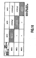
FIG. 10 is a table illustrating ratios of the twice reflected light rays to the signal light when the reflectances of the Ref(i) and ref(i) inFIG. 9 are assumed to be R(i) and r(i) (where 1 <= i <= 3). As shown inFIG. 10 , when Ref (i-1) reflection occurs following ref(i), the ratios of the twice reflected light rays to the signal light are in the order of a square of the reflectance at the reflection point. However, when the reflection Ref(i-2) or Ref(i-3) occurs following ref (i), the ratio of the twice reflected light rays to the signal light is increased by a square of the gain of the SOA passed through as compared with the order of the square of the reflectance at the reflection point. - Although
FIG. 10 shows the case where n = 2, when n SOAs are arranged in the multistage connection, the reflections Ref(i-2), Ref(i-3), ··, and Ref(0) following ref(i) have the ratios of the reflected light rays to the signal light greater than the reflection Ref(i-1) following ref(i) by squares of the gains of Si-1, Si-1 + Si-2, ··,Si-1 + Si-2 + ·· + S1 (where 1 <= i <= n+1). - Accordingly, to allow the reflection Ref (i-1) following ref (i), and to prevent reflections Ref (i-2), Ref(i-3), ··, and Ref(0) following ref (i), it is enough to insert optical isolators at every alternate optical path (x1, x2, ··, xi, ··, xn-1).
-
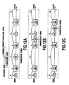
FIGs. 11A-11C are diagrams illustrating configurations of the optical modulation apparatus of the first example , into which optical isolators are inserted at every alternate optical path. Here, O1 and O2 each designate an optical isolator. The first optical isolator O1 is inserted into the first optical path x1 between the input-side transmission path and the first SOA S1, and the second optical isolators O1 is inserted into the third optical path x3 between the second SOA S2 and third SOA S3. Thus, the present embodiment is characterized by inserting the optical isolators at every alternate optical path. - In addition, the present examples each include n = 3 SOAs, and use any one of them as an optical intensity modulator (MOD) by carrying out intensity modulation of injection current by a transmission signal. Specifically, the third SOAS3 is used as the optical intensitymodulator in
FIG. 11A , the second SOA S2 is used as the optical intensity modulator inFIG. 11B , and the first SOA S1 is used as the optical intensity modulator inFIG. 11C . - As for the foregoing relationship of the arrangement of the optical isolators and the optical intensity modulator, it is the same when the number of the SOAs is two or four or more.
- The configuration of the embodiment can implement the system that can compensate for the optical power loss on the transmission path and achieve the modulation operation simultaneously in the optical communication system having the light source for outputting the continuous wave and the optical intensity modulator, which are placed at a distance via the transmission path.
-
FIGs. 12A-12C are diagrams each showing a configuration of the optical modulation apparatus of a second example . The present example is a variation of the first example, which has an optical intensity modulator M inserted between any two of three SOAs S1, S2 and S3 constituting the optical amplifier. -
FIG. 12A shows a configuration having the optical intensity modulator M inserted in to a section in which neither the optical isolator O1 nor O2 is inserted. Although the example is shown here which has the optical intensity modulator M inserted into the second optical path (optical connection means) x2 between the first and second SOAs S1 and S2, the optical intensity modulator M can be inserted into a fourth optical path x4 between the third SOAS3 and the output terminal. In the latter case, however, it is necessary to use an optical intensity modulator M that can handle the optical power amplified by the final stage SOA S3. - In the configuration of
FIG. 12A , the intensity modulation is carried out twice by the optical intensity modulator M until the continuous wave output from the first SOA S1 interferes with the twice reflected light ray of the continuous wave at the second SOA S2 and first SOA S1. Accordingly, the ratio of the twice reflected light ray to the signal light is relatively small as compared with the case where no optical intensity modulator M is inserted. -
FIG. 12B shows a configuration that has the optical intensity modulator M inserted into the section into which the optical isolator O2 is inserted. Although the example shown has the optical intensity modulator M inserted into the third optical path x3 between the second and third SOAs S2 and S3, the optical intensity modulator M can be inserted into the first optical path X1 between the input terminal and the first SOA S1. In the latter case, however, it is necessary to consider that the input power to the SOA S1 is reduced and the SNR is deteriorated because of the loss of the optical intensity modulator M. Incidentally, the order of connection of the optical isolator O2 and the optical intensity modulator M is arbitrary as shown inFIGs. 12B-12C . - As the optical intensity modulator M used in the present embodiment, an electro absorption optical intensity modulator (EA modulator) can be used, for example. Since the foregoing first embodiment uses the SOA as the optical intensity modulator, it is difficult to carry out the modulation operation of the order of G (bps) or more. In contrast, the EA modulator used as the optical intensity modulator can handle the modulation operation of the order of 40G (bps).
- An embodiment of the optical modulation apparatus in accordance with the present invention relates to a system that can achieve the stable amplifying function by reducing the effect of the reflected light rays on the end faces of the bidirectional optical amplifiers by imposing the following numerical limitation on the gain of the amplifier in the foregoing system configuration including the bidirectional optical amplifiers as shown in
FIG. 4 . The numerical limitation on the amplifier gain in accordance with the present invention will be described below. - As shown in
FIG. 4 , there are two reflected light rays from the ends of the bidirectionaloptical amplifier 409 or 415: first reflectedlight 1 travels in the same direction as the modulated light, and second reflectedlight 2 travels in the same direction as the continuous wave. The continuous wave undergoes the intensity modulation and becomes the modulated light. Since the reflectedlight 2 travels through the same path as the continuous wave, the modulated light is finally provided with the reflectedlight 1 and reflectedlight 2. The modulated light interferes with the same polarization direction components of the reflectedlight 1 and reflectedlight 2, thereby generating intensity fluctuations as beat noise. Next, a method will be described of quantitatively showing the effect of the reflectedlight 1 and reflectedlight 2 on the modulated light. - The following are assumed here.
- The multiple reflection light rays, which are reflected off the first end face of the bidirectional
optical amplifier 409 or 415 and then reflected off the second end face thereof again, are assumed to be sufficiently small and are neglected. - • The mark-to-space ratio of the transmission signal is assumed to be 1/2. (Since the continuous mark or space in the data signal train makes it difficult to extract a clock signal at the reception of the signal, a technique of making the mark-to-space ratio nearly 1/2 is usually employed such as scramble in the SDH (synchronous digital hierarchy) or 8 B→10 B (bel) conversion in the gigabit ether.)
- Assume that the input continuous wave power to the bidirectional
optical amplifiers 409 and 415, the gain of the bidirectionaloptical amplifiers 409 and 415, the difference between the modulated light output power and the input continuous wave power to theoptical intensity modulators light 1, and the power of the reflectedlight 2 are represented by g2x, r' and g2x2r', respectively. - Since the problem to be considered here is the interference between the modulated light and the reflected light, it is enough to consider only the effect of the reflected light when the modulated light is at the mark. Since the transmission signal has the mark-to-space ratio of 1/2, the mark level power of the output modulated light of the optical modulator, and the mark level power of the ref lected
light 2 are 2g2x and 4g2x2r', respectively. Here, since the probability is 1/2 that the modulated light and reflectedlight 2 are mark at the same time in the optical modulator output, the effect of the reflectedlight 2 is halved. Accordingly, the power ratio between the modulated light and the total reflected light when the modulated light is at the mark is expressed by


light 1 becomes equal to that of the reflectedlight 2. - In actuality, since the reflected light interferes with the modulated light, the foregoing description is effective only for deriving expression (4) above that optimizes the SNR. The quantitative estimation of the effect of the reflected light on the modulated light can be made as follows.
- Consider the case where the optical modulator output is received through the
optical circulator 417 or the like. Assume that mark-side optical electrical field of the modulated light is E 0 exp[i(ω ct+φ0)], mark-side optical electrical field of the reflectedlight 1 is E 1 exp[i(ω ct+ φ1)], and mark-side optical electrical field of the reflectedlight 2 is E 2 exp[i(ω ct + φ2)], then the optical electrical field before reception is expressed by the following expression.
- The received optical current is given by the following expression by neglecting all the coefficients required.

light 1; the beat (interference) between the modulated light and the reflectedlight 2; the power of the reflectedlight 1; the power of the reflectedlight 2; and the beat (interference) between the reflectedlight 1 and the reflectedlight 2. The fourth to sixth terms are negligible because the reflected light is small as compared with the modulated light. Here, considering the second and third terms, normalized beat noise power is defined as follows.
- The beat noise when a plurality of reflection points are involved can be handled as Gaussian distribution with a variance given by expression (7). On the contrary, when the number of the reflection points is small, excessive estimation of the beat noise is made.
- The above discussion so far considers as the reflected light rays the reflected
light 1 and reflectedlight 2 from both end faces of the bidirectionaloptical amplifiers 409 and 415. In practice, however, besides the end face reflections at the bidirectionaloptical amplifiers 409 and 415, there are input/output terminal reflections of a variety of optical devices inserted into the system, and reflections by optical connectors, and the reflected light rays from these reflection points undergo the gains of the bidirectionaloptical amplifiers 409 and 415, and become nonnegligible depending on their reflectances. In such a case, considering the end face reflectance r used in the discussion up to now as the sum of the reflectances of the reflection points other than the end face reflection, it can be correctly said that the estimation of the effect of the reflected light rays using the variance given by expression (7) is appropriate. On the other hand, when the reflections from both end faces of the bidirectionaloptical amplifiers 409 and 415 are dominant, it is appropriate to consider the foregoing estimation as the worst case. - The foregoing discussion is made on the analogy of the paper IEEEJ. LightwaveTchnol., vol. 14, no. 6, pp. 1097-1105 , 1996 describing a method of quantitatively estimating the effect of the coherent crosstalk of an arrayed-waveguide grating (AWG). However, in the present optical modulation apparatus, since the probability that the reflected
light 2 is mark when the modulated light is mark is 1/2, the foregoing expression (7) can be rewritten by the following expression.
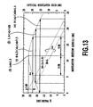
-
FIG. 13 shows calculation results using the foregoing expression (8). InFig.13 , the horizontal axis represents a modulation section loss (L) [dB], and the vertical axis represents a Q value [dB] on the left side, and the optical modulation apparatus gain [dB] on the right side. As for the optical modulation apparatus gain, are drawn both 2G-(L-3.0) [dB] without considering the 3dB modulation loss in the modulation section (optical intensity modulators) 411 or 419, and 2G - L [dB] considering the 3dB modulation loss. The Q value here refers to an evaluation parameter that determines the signal-to-noise ratio (SNR) of the modulated light proposed in IEEE Photon. Technol. Lett. Vol. 5, no. 3, pp. 304-306, and is defined by the following expression
- It is assumed in the calculation that the input continuous wave power to the
optical modulation apparatuses FIG. 13 , ranges (α), (β), (γ) and (δ) are as follows.
- The optical modulation section loss region that ensures the
optical modulator gain 2G - (L - 3.0) >= 0, and the Q value with theoptical modulator gain 2G - (L - 3.0) = 0 (dB).
- The optical modulation section loss region that ensures the
optical modulator gain 2G - L >= 0, and the Q value with theoptical modulator gain 2G - L = 0 (dB).
- The region where the Q value is within 3 dB of the maximum value.

- The modulation section loss that takes the maximum Q value.
- As for the region (δ), it is as described above. In addition, the upper limit values of L in the regions (α) and (β) indicate that the optical modulation gain is equal to or greater than 0 [dB]. Furthermore, as for the modulation section loss L, itsvalueislogically determined from the fact that the Q value curve has the left-right symmetry as described above.
- The Q value becomes within 3 dB with respect to the maximum value when 5.5 [dB] <= L <= 17.5 [dB], that is, (G + 1.5)- 6 [dB] <= L <= (G + 1.5) + 6 [dB]. The range of L is independent of the value G. In fact, solving the quadratic equation for x, which is obtained by substituting the value x defined in the foregoing expression (3) into the foregoing expression (1), and by making the half of that result (3 dB reduction) equal to expression (1), gives the following solution.


- Accordingly, with maintaining the gain, the optical modulation apparatus can keep the ratio low of the reflected light to the modulated light with placing the modulation section loss L in a given range in the region (α) (such as (β), (γ) and (δ)). In this case, as is clear from
FIG. 13 , the ratio can be reduced as the modulation section loss L approaches L = G + 1.5 at (δ). -
FIG. 14 shows a configuration of the optical modulation apparatus of a third example. The optical modulation apparatus of the present example implements a stable amplifying function by reducing the effect of the reflected light from the end faces of the bidirectional optical amplifiers by inserting polarization rotation means. - As shown in
FIG. 14 , the present system is a multi-wavelength collective optical modulation apparatus that includes apolarization demultiplexer 501 for separating the input multi-wavelength light from the output modulated light by the difference in the plane of polarization; awave length multi-demultiplexer 502 for demultiplexing the multi-wavelength light into every predetermined wavelengths; bidirectionaloptical amplifiers 503 for bidirectionally amplifying the individual single wavelength optical powers demultiplexed; polarization rotation means 504 each for bidirectionally rotating the plane of polarization of the single wavelength light;optical intensity modulators 505 each for bidirectionally modulating the intensity of the single wavelength light; andoptical reflectors 506 for feeding the modulated single wavelength light rays output from theoptical intensity modulators 505 back to the bidirectionaloptical amplifiers 503. - As the
polarization demultiplexer 501, a polarization beam splitter (PBS) is applicable. Alternatively, a configuration is also possible which has thewavelength multi-demultiplexer 502 produce output light via an optical circulator or an optical coupler, and extracts the light whose polarization shifts from that of the input light by 90 degrees by using a polarizer. - As the
wavelength multi-demultiplexer 502, an AWG is applicable, for example. The AWG has the light incident onto an input waveguide output from a different output waveguide in accordance with the wavelength. The AWG has reversibility, and can multiplex a plurality of wavelength light rays into a single output waveguide. - As the bidirectional
optical amplifiers 503, SOAs can be used, for example. The SOA is an optical amplifier for amplifying the light traveling through the active layer in the semiconductor by stimulated emission by reducing the reflection from the cavity end faces of a semiconductor laser. As the bidirectionaloptical amplifiers 503, fiber amplifiers such as erbium doped fiber amplifiers (EDFAs) can also be used. However, since the fiber amplifier is composed of a semiconductor laser for outputting pumping light, a doped fiber doped with erbium and the like, and a coupler for coupling the pumping light to the doped fiber, it will be more expensive than the SOA from the viewpoint of the number of the components. Accordingly, the SOA has a cost advantage. - The polarization rotation means 504 is installed between the bidirectional
optical amplifiers 503 and theoptical intensity modulators 505. As the polarization rotation means 504, aquarter-wave plate or a Faraday cell is applicable. Alternatively, a Faraday mirror is usable which attaches a reflecting mirror to an output end of the Faraday cell. - As the
optical intensity modulators 505, a Mach Zehnder type optical intensitymodulator or an electro absorption optical intensity modulator (EA modulator) is applicable, for example. They have a function of carrying out intensity modulation of the single wavelength light by a data signal. These optical intensity modulators can achieve the intensity modulation by a 40 G(bps) order modulation signal at a practical level. - As the
optical reflectors 507, a mirror having metal coating or dielectric multi-layer coating is applicable, for example. As a reflecting mirror for a particular wavelength, a diffraction grating or fiber Bragg grating is also applicable to the optical reflector. In addition, as an application of the fiber Bragg grating, an optical reflector can be used inwhich a diffraction grating is directlywritten on an optical waveguide. - One of the output ports of the
polarization demultiplexer 501 is optically connected to the input waveguide of thewavelength multi-demultiplexer 502 via a spatial optical system or an optical waveguide. The output waveguides of thewavelength multi-demultiplexer 502 are optically connected to first ports of the bidirectionaloptical amplifiers 503 via a spatial optical system or optical waveguides. Second ports of the bidirectionaloptical amplifiers 503 are optically connected to first ports of the polarization rotation means 504 via a spatial optical system or optical waveguides as well. Second ports of the polarization rotation means 504 are optically connected to first ports of theoptical intensity modulators 505 via a spatial optical system or optical waveguides as well. Second ports of theoptical intensity modulators 505 are optically connected to theoptical reflectors 507 via a spatial optical system or optical waveguides as well. - In the present example, the
polarization demultiplexer 501 separates the inputs to theoptical intensity modulators 505 from their modulated light outputs. However, in the case where the quarter-wave plates are used as the polarization rotation means 504, the angles of the planes of polarization of the input light rays and the output light rays differ by 90 degrees. Accordingly, the input light rays can be separated from the output light rays by extracting the particular polarized waves from the output light rays by thepolarization demultiplexer 501. - The multi-wavelength light input to the
wavelength multi-demultiplexer 502 via the input waveguide is demultiplexed to the individual wavelengths by thewave length multi-demultiplexer 502. Each single wavelength light passing through the demultiplexing is led to corresponding one of the bidirectionaloptical amplifiers 503 to have its power amplified. - The bidirectional
optical amplifiers 503 bring about signal degradation because of the gain scrambling between the continuous waves and modulated light rays in the saturation region of the gain. Accordingly, as illustrated inFIG. 5 , it is preferable that the bidirectionaloptical amplifiers 503 be used in the unsaturated region of the gain in which the gain (the vertical axis) is maintained at a constant value as long as the sum of the output powers (the horizontal axis) (or the sum of input powers) of the continuous waves and the modulated light from the bidirectionaloptical amplifiers 503 is equal to or less than a particular output power (or input power). - The continuous waves (single wavelength light rays) whose powers are amplified by the individual bidirectional
optical amplifiers 503 are input to the corresponding polarization rotation means 504. The polarization rotation means 504 rotate the planes of polarization of the continuous waves by 45 degrees, and supply them to theoptical intensity modulators 505. Theoptical intensity modulators 505 carry out the intensity modulation of the continuous waves by modulation signals (data signals). The modulated single wavelength light rays are output from the optical reflector side ports of theoptical intensity modulators 505, and are input to theoptical reflectors 507. The modulated light rays reflected by theoptical reflectors 507 pass through theoptical intensity modulators 505 again, and are input to the polarization rotation means 504. The modulated light rays have their planes of polarization rotated by 45 degrees by the polarization rotation means 504, and are input to the bidirectionaloptical amplifiers 503 which amplify the optical powers again. Since the output modulated light rays of the bidirectionaloptical amplifiers 503 have the planes of polarization different by 90 degrees from those of the input light rays, thepolarization demultiplexer 501 can separate the output light rays from the input light rays. Accordingly, the output modulated light rays from the bidirectionaloptical amplifiers 503 are multiplexed by thewavelength multi-demultiplexer 502, and are output from the output port of thepolarization demultiplexer 501 to a system outside. - To operate the optical amplifier in the bidirectional mode, the optical amplifier cannot include an optical isolator. Accordingly, it is necessary to consider the effect of the end face reflections from both terminals of the optical amplifying paths. As shown in
FIG. 4 , there are two reflected light rays in the bidirectional transmission (reflectedlight ray 1 and reflected light ray 2). The reflectedlight ray 1 propagates in the same direction as the modulated light, and the reflectedlight ray 2 in the same direction as the continuous waves. The continuous waves undergo the intensity modulation and become modulated light, and the reflectedlight ray 2 travels through the same path as the continuous waves. Consequently, if the planes of polarization of the reflectedlight rays light ray 1 and reflectedlight ray 2. As a result, the modulated light rays interfere with the same polarization direction components of the reflectedlight ray 1 and reflectedlight ray 2, causing the intensity fluctuations as the beat noise. - However, in the configuration of the present example having the polarization rotation means 504, the reflected
light ray 1 and reflectedlight ray 2 from the bidirectionaloptical amplifiers 503 are orthogonal to the polarization direction of the continuous waves or modulated light rays traveling in the same direction as indicated by arrows enclosed by circles representing the directions of the planes of polarization inFIG. 15 . Since the reflectedlight ray 1 and the modulated light rays have the polarization directions orthogonal to each other, thepolarization demultiplexer 501 can separate them at the output. In addition, the reflectedlight ray 2 has the polarization direction orthogonal to that of the continuous waves, and maintain the polarization relationship after the reflectedlight ray 2 passes through the intensity modulation and become modulated light rays. Thus, the reflectedlight ray 2 can be separated from the continuous waves so as to output by thepolarization demultiplexer 501 in the same manner as the reflectedlight ray 1. As a result, the intensity fluctuations due to the interference between the two light rays can be eliminated. - According to the configuration of the present example, as shown in
Fig.15 , the planes of polarization of the light rays are the same in the two directions on the paths from the outputs of the polarization rotation means 504 to the return to the polarization rotation means 504 after the reflection by theoptical reflectors 507. Consequently, it is possible to use as theoptical intensity modulators 505 an optical intensity modulator such as LiNbO3 Mach Zehnder type optical intensity modulator capable of carrying out modulation only for a single input polarized wave. -
FIG. 16 shows a configuration of the optical modulation apparatus of a fourth example. The system of the fourth example haspolarizers 506, which enable only single polarized waves to pass through, interposed before or after theoptical intensity modulators 505 of the multi-wavelength collective optical modulation apparatus in the foregoing fourth embodiment (inFIG. 16, they are interposed after). Since the remaining configuration is the same as that of the third example, the detailed description thereof is omitted here. - Generally speaking, the polarization extinction ratio between two orthogonal polarized waves deteriorates markedly when coupling a plurality of optical devices and fibers. According to the configuration shown in
FIG. 16 , since the planes of polarization of the light rays are the same in the two directions on the paths from the outputs of the polarization rotation means 504 to the return to the polarization rotation means 504 after the reflection by theoptical reflectors 507, thepolarizers 506 can be inserted into the optical paths. The insertion of thepolarizers 506 can recover the polarization extinction ratio degraded. - The present invention has been described by way of example of preferred embodiments. However, the embodiments in accordance with the present invention are not limited to the foregoing examples, and a variety modifications such as replacement, changes, addition, increase or decrease in the number, or the changes in the geometry of the components of the configuration are all included in the embodiments in accordance with the present invention as long as they fall within the scope of the claims.
Claims (6)
- An optical modulation apparatus (405, 407) comprising:bidirectional optical amplifying means (409, 415) for transmitting a continuous wave with a single wavelength bidirectionally, and for providing the single wavelength light with a gain;optical intensity modulation means (411, 419) for carrying out intensity modulation of the continuous wave whose optical power is amplified by said bidirectional optical amplifying means, by a transmission signal; andoptical regression means (413, 417) for feeding the continuous wave passing through the intensity modulation by said optical intensity modulation means back to said optical intensity modulation means, or back to said bidirectional optical amplifying means directly, characterized in thatsaid transmission signal has a mark-to-space ratio of practically 1/2; andsaid optical intensity modulation means (411, 419) is configured with a modulation section loss L in a range from 0 dB to 2G+3.0 dB, wherein the modulation section loss is defined as a difference between optical power of the input continuous wave to said optical intensity modulation means and optical power of output modulated light from said optical intensity modulation means and G is the gain of said bidirectional optical amplifying means, and wherein L and G are indicated in dB.
- The optical modulation apparatus as claimed in claim 1, wherein said optical intensity modulation means (411, 419) is configured with the modulation section loss L of G+1.5 dB.
- The optical modulation apparatus as claimed in claims 1 or 2, wherein said bidirectional optical amplifying means (409, 415) is operated in an unsaturated region of the gain.
- The optical modulation apparatus as claimed in any one of claims 1-3, wherein said optical intensity modulation means (411, 419) is a reflection type optical intensity modulator having an optical reflector (413) constituting said optical regression means at a rear end of said optical intensity modulation means.
- The optical modulation apparatus as claimed in any one of claims 1-3, wherein said optical intensity modulation means (411, 419) is a transmission-type optical intensity modulator that is installed in an optical loop constituting said optical regression means formed via an optical circulator (417).
- A system of optical modulation apparatuses for multi-wavelength collective optical modulating comprising:a plurality of said optical modulation apparatuses (405, 407) recited in any one of claims 1 to 5 installed equal in number to multiplexed wavelengths;wavelength multi-demultiplexing means (403) for demultiplexing continuous waves which are wavelength division multiplexed, for supplying each single wavelength to one of said plurality of optical modulation apparatuses, and for multiplexing modulated light rays output from said plurality of optical modulation apparatuses to be output; andan optical circulator (401) interposed at a position of a waveguide used for inputting and outputting the multiplexing modulated light rays to or from said wavelength multi-demultiplexing means (403).
Priority Applications (2)
| Application Number | Priority Date | Filing Date | Title |
|---|---|---|---|
| EP10175374A EP2253992B1 (en) | 2003-06-19 | 2004-06-16 | Optical modulation apparatus |
| EP10175373A EP2253991B1 (en) | 2003-06-19 | 2004-06-16 | Optical modulation apparatus |
Applications Claiming Priority (4)
| Application Number | Priority Date | Filing Date | Title |
|---|---|---|---|
| JP2003174499 | 2003-06-19 | ||
| JP2003174491 | 2003-06-19 | ||
| JP2003195735 | 2003-07-11 | ||
| PCT/JP2004/008762 WO2004113998A1 (en) | 2003-06-19 | 2004-06-16 | Optical modulating device |
Related Child Applications (2)
| Application Number | Title | Priority Date | Filing Date |
|---|---|---|---|
| EP10175374.7 Division-Into | 2010-09-06 | ||
| EP10175373.9 Division-Into | 2010-09-06 |
Publications (3)
| Publication Number | Publication Date |
|---|---|
| EP1635211A1 EP1635211A1 (en) | 2006-03-15 |
| EP1635211A4 EP1635211A4 (en) | 2010-02-24 |
| EP1635211B1 true EP1635211B1 (en) | 2011-08-17 |
Family
ID=33545087
Family Applications (3)
| Application Number | Title | Priority Date | Filing Date |
|---|---|---|---|
| EP10175373A Expired - Fee Related EP2253991B1 (en) | 2003-06-19 | 2004-06-16 | Optical modulation apparatus |
| EP10175374A Expired - Fee Related EP2253992B1 (en) | 2003-06-19 | 2004-06-16 | Optical modulation apparatus |
| EP04746231A Expired - Fee Related EP1635211B1 (en) | 2003-06-19 | 2004-06-16 | Optical modulation apparatus |
Family Applications Before (2)
| Application Number | Title | Priority Date | Filing Date |
|---|---|---|---|
| EP10175373A Expired - Fee Related EP2253991B1 (en) | 2003-06-19 | 2004-06-16 | Optical modulation apparatus |
| EP10175374A Expired - Fee Related EP2253992B1 (en) | 2003-06-19 | 2004-06-16 | Optical modulation apparatus |
Country Status (4)
| Country | Link |
|---|---|
| US (2) | US7336414B2 (en) |
| EP (3) | EP2253991B1 (en) |
| JP (1) | JP3850866B2 (en) |
| WO (1) | WO2004113998A1 (en) |
Families Citing this family (27)
| Publication number | Priority date | Publication date | Assignee | Title |
|---|---|---|---|---|
| JP3850866B2 (en) | 2003-06-19 | 2006-11-29 | 日本電信電話株式会社 | Light modulator |
| KR100539928B1 (en) * | 2003-08-29 | 2005-12-28 | 삼성전자주식회사 | Multi-wavelength light source and wavelength division multiplexing system using the same |
| KR20070108422A (en) * | 2006-01-09 | 2007-11-12 | 한국전자통신연구원 | Rsoa and the operating system based on downstream optical signal reuse method with feed-forward current injection |
| KR100908239B1 (en) * | 2006-12-06 | 2009-07-20 | 한국전자통신연구원 | Channel Pass / Coupling Optical Module and Channel Pass / Coupling Method in OMD Node Using the Same |
| US20100008671A1 (en) * | 2008-07-08 | 2010-01-14 | Standard Scientific Technologies, Inc. | High Density Wave Channel Optical Data Communications |
| US20100021164A1 (en) * | 2008-07-25 | 2010-01-28 | Nortel Networks Limited | Wdm pon rf/video broadcast overlay |
| KR100987793B1 (en) * | 2008-10-10 | 2010-10-13 | 한국전자통신연구원 | Reflective semiconductor optical amplifier and optical signal treating method using the same |
| GB0819616D0 (en) | 2008-10-25 | 2008-12-03 | Ct For Integrated Photonics Th | Wavelenghth division multiplexing transmission eqipment |
| EP2404394B1 (en) * | 2009-03-04 | 2016-10-05 | Xieon Networks S.à r.l. | Method for data processing in an optical network component and optical network component |
| US8345349B2 (en) * | 2009-05-27 | 2013-01-01 | Hewlett-Packard Development Company, L.P. | Compact optical resonators |
| US8655176B2 (en) * | 2010-01-27 | 2014-02-18 | Telcordia Technologies, Inc. | System and methods for converting a temporally short and spectrally broad optical pulse into a train of spectrally narrow optical pulses |
| EP2372936A1 (en) * | 2010-03-29 | 2011-10-05 | Alcatel Lucent | Photonic integrated transmitter |
| US8755693B2 (en) * | 2011-05-16 | 2014-06-17 | Eastern Optx, Inc. | Bi-directional, compact, multi-path and free space channel replicator |
| EP2753009B1 (en) * | 2011-09-29 | 2018-01-03 | Huawei Technologies Co., Ltd. | Method and system for transmitting data information by using optical signals |
| EP2575276B1 (en) * | 2011-09-30 | 2016-08-10 | Alcatel Lucent | Integrated node architecture for optical packet rings |
| US9025241B2 (en) * | 2011-10-14 | 2015-05-05 | Kotura, Inc. | Gain medium providing laser and amplifier functionality to optical device |
| EP2929640B1 (en) * | 2012-12-10 | 2019-03-27 | Telefonaktiebolaget LM Ericsson (publ) | Power control in bidirectional wdm optical link |
| CA2896006A1 (en) * | 2012-12-21 | 2014-06-26 | David Welford | Systems and methods for narrowing a wavelength emission of light |
| US9158138B2 (en) | 2013-05-14 | 2015-10-13 | Coriant Advanced Technology, LLC | Ultra-responsive phase shifters for depletion mode silicon modulators |
| JP2016171156A (en) * | 2015-03-12 | 2016-09-23 | ソニー株式会社 | Optical amplification device and light source device |
| JP2018032824A (en) * | 2016-08-26 | 2018-03-01 | 国立大学法人東北大学 | Optical pulse signal generating device, laser processing device and bio imaging device |
| US10971861B2 (en) * | 2017-02-24 | 2021-04-06 | Michael S. Gzybowski | Polarized electrical plug and adaptor with modular orientation verification |
| WO2019049952A1 (en) * | 2017-09-08 | 2019-03-14 | 古河電気工業株式会社 | Optical module |
| US11082143B2 (en) * | 2017-11-21 | 2021-08-03 | Cable Television Laboratories, Inc. | Systems and methods for full duplex coherent optics |
| US10917175B2 (en) | 2017-11-21 | 2021-02-09 | Cable Television Laboratories, Inc. | Systems and methods for full duplex coherent optics |
| US10735097B2 (en) * | 2017-11-21 | 2020-08-04 | Cable Television Laboratories, Inc | Systems and methods for full duplex coherent optics |
| US10892829B2 (en) * | 2017-11-21 | 2021-01-12 | Cable Television Laboratories, Inc | Systems and methods for full duplex coherent optics |
Family Cites Families (15)
| Publication number | Priority date | Publication date | Assignee | Title |
|---|---|---|---|---|
| US5657148A (en) | 1996-05-07 | 1997-08-12 | Lucent Technologies Inc. | Apparatus and method for a single-port modulator having amplification |
| JPH10173597A (en) | 1996-12-06 | 1998-06-26 | Nec Corp | Optical equalizer |
| JPH1146030A (en) | 1997-05-29 | 1999-02-16 | Nec Corp | Optical signal relaying and amplifying apparatus and optical level regulator |
| US6134250A (en) * | 1998-05-14 | 2000-10-17 | Lucent Technologies Inc. | Wavelength-selectable fiber ring laser |
| SE513096C2 (en) * | 1998-10-02 | 2000-07-10 | Ericsson Telefon Ab L M | Method and apparatus for channel equalization of wavelength multiplexed optical systems |
| JP2002111634A (en) * | 2000-09-29 | 2002-04-12 | Kddi Submarine Cable Systems Inc | Optical transmission apparatus |
| US7019893B2 (en) * | 2001-02-12 | 2006-03-28 | Metrophotonics Inc. | Optical dynamic gain amplifier |
| JP2002318374A (en) * | 2001-04-20 | 2002-10-31 | Nippon Telegr & Teleph Corp <Ntt> | Multi-wavelength batch optical modulating device |
| JP3732804B2 (en) | 2001-06-13 | 2006-01-11 | 日本電信電話株式会社 | Multi-wavelength optical modulation circuit and wavelength-multiplexed optical signal transmitter |
| US7127168B2 (en) | 2001-06-13 | 2006-10-24 | Nippon Telegraph And Telephone Corporation | Multi-wavelength optical modulation circuit and wavelength-division multiplexed optical signal transmitter |
| JP2003018853A (en) | 2001-06-28 | 2003-01-17 | Fuji Electric Co Ltd | Common mode current reduction method |
| US6522462B2 (en) * | 2001-06-29 | 2003-02-18 | Super Light Wave Corp. | All optical logic using cross-phase modulation amplifiers and mach-zehnder interferometers with phase-shift devices |
| KR100396510B1 (en) * | 2001-09-11 | 2003-09-02 | 삼성전자주식회사 | Dispersion-compensated optical fiber amplifier |
| JP3850866B2 (en) | 2003-06-19 | 2006-11-29 | 日本電信電話株式会社 | Light modulator |
| US7123407B2 (en) * | 2005-01-20 | 2006-10-17 | Korea Institute Of Science And Technology | Apparatus and method for realizing all-optical NOR logic device using gain saturation characteristics of a semiconductor optical amplifier |
-
2004
- 2004-06-16 JP JP2005505047A patent/JP3850866B2/en not_active Expired - Fee Related
- 2004-06-16 EP EP10175373A patent/EP2253991B1/en not_active Expired - Fee Related
- 2004-06-16 EP EP10175374A patent/EP2253992B1/en not_active Expired - Fee Related
- 2004-06-16 US US10/534,310 patent/US7336414B2/en not_active Expired - Fee Related
- 2004-06-16 WO PCT/JP2004/008762 patent/WO2004113998A1/en active Application Filing
- 2004-06-16 EP EP04746231A patent/EP1635211B1/en not_active Expired - Fee Related
-
2007
- 2007-02-13 US US11/674,576 patent/US7474460B2/en not_active Expired - Fee Related
Also Published As
| Publication number | Publication date |
|---|---|
| EP2253991A2 (en) | 2010-11-24 |
| JPWO2004113998A1 (en) | 2006-07-20 |
| EP2253991B1 (en) | 2012-03-14 |
| EP1635211A4 (en) | 2010-02-24 |
| EP2253991A3 (en) | 2010-12-22 |
| US7336414B2 (en) | 2008-02-26 |
| EP2253992B1 (en) | 2012-03-14 |
| US7474460B2 (en) | 2009-01-06 |
| US20060024066A1 (en) | 2006-02-02 |
| EP1635211A1 (en) | 2006-03-15 |
| US20070127113A1 (en) | 2007-06-07 |
| JP3850866B2 (en) | 2006-11-29 |
| WO2004113998A1 (en) | 2004-12-29 |
| EP2253992A2 (en) | 2010-11-24 |
| EP2253992A3 (en) | 2010-12-22 |
Similar Documents
| Publication | Publication Date | Title |
|---|---|---|
| EP1635211B1 (en) | Optical modulation apparatus | |
| US9065243B2 (en) | Optical amplifier | |
| EP0981189B1 (en) | Method and apparatus using four wave mixing for optical wavelength conversion | |
| US6654561B1 (en) | Method and apparatus for measuring optical signal-to-noise ratio, and pre-emphasis method and optical communication system each utilizing the method | |
| KR101059310B1 (en) | Method and apparatus for integrating laser sources and detectors for passive optical networks | |
| RU2166839C2 (en) | Device for damping optical noise caused by four-wave displacement | |
| US6603593B2 (en) | Optical transmission link including raman amplifier | |
| US9203543B2 (en) | Passive optical networks | |
| KR20040040659A (en) | Passive optical network using loop back of multi-wavelength light generated at central office | |
| US6519080B2 (en) | Optical amplifier and optical transmission system | |
| US7702201B2 (en) | Gain flattening utilizing a two-stage erbium-based amplifier | |
| JP4537351B2 (en) | Light modulator | |
| Iannone et al. | A 160-km transparent metro WDM ring network featuring cascaded erbium-doped waveguide amplifiers | |
| WO2008141442A1 (en) | Transmitter and receiver for optical communication systems | |
| CN100555027C (en) | Optic modulating device | |
| JP2003188853A (en) | Multiple wavelength optical transmitter | |
| KR20000026692A (en) | Optical transmission device by using noise light source having improved signal-to-noise ratio | |
| Turkiewicz | Applications of O-band semiconductor optical amplifiers in fibre-optic telecommunication networks | |
| Marra et al. | A WDM fiber-radio system with improved optical spectral efficiency incorporating remote LO delivery and novel FBG optical filtering | |
| Ali | Analytical investigation of 8-channel optical wavelength division multiplexing communication system | |
| Mathlouthi et al. | Transmitter and receiver for optical communication systems | |
| Ho et al. | Distortion and crosstalk reduction in semiconductor laser amplifier for WDM systems |
Legal Events
| Date | Code | Title | Description |
|---|---|---|---|
| PUAI | Public reference made under article 153(3) epc to a published international application that has entered the european phase |
Free format text: ORIGINAL CODE: 0009012 |
|
| 17P | Request for examination filed |
Effective date: 20050511 |
|
| AK | Designated contracting states |
Kind code of ref document: A1 Designated state(s): DE FR GB |
|
| DAX | Request for extension of the european patent (deleted) | ||
| RBV | Designated contracting states (corrected) |
Designated state(s): DE FR GB |
|
| A4 | Supplementary search report drawn up and despatched |
Effective date: 20100127 |
|
| 17Q | First examination report despatched |
Effective date: 20100512 |
|
| GRAP | Despatch of communication of intention to grant a patent |
Free format text: ORIGINAL CODE: EPIDOSNIGR1 |
|
| GRAS | Grant fee paid |
Free format text: ORIGINAL CODE: EPIDOSNIGR3 |
|
| GRAA | (expected) grant |
Free format text: ORIGINAL CODE: 0009210 |
|
| RTI1 | Title (correction) |
Free format text: OPTICAL MODULATING APPARATUS |
|
| RTI1 | Title (correction) |
Free format text: OPTICAL MODULATION APPARATUS |
|
| AK | Designated contracting states |
Kind code of ref document: B1 Designated state(s): DE FR GB |
|
| REG | Reference to a national code |
Ref country code: GB Ref legal event code: FG4D |
|
| REG | Reference to a national code |
Ref country code: DE Ref legal event code: R096 Ref document number: 602004033996 Country of ref document: DE Effective date: 20111013 |
|
| PLBE | No opposition filed within time limit |
Free format text: ORIGINAL CODE: 0009261 |
|
| STAA | Information on the status of an ep patent application or granted ep patent |
Free format text: STATUS: NO OPPOSITION FILED WITHIN TIME LIMIT |
|
| 26N | No opposition filed |
Effective date: 20120521 |
|
| REG | Reference to a national code |
Ref country code: DE Ref legal event code: R097 Ref document number: 602004033996 Country of ref document: DE Effective date: 20120521 |
|
| PGFP | Annual fee paid to national office [announced via postgrant information from national office to epo] |
Ref country code: DE Payment date: 20130628 Year of fee payment: 10 Ref country code: GB Payment date: 20130620 Year of fee payment: 10 |
|
| PGFP | Annual fee paid to national office [announced via postgrant information from national office to epo] |
Ref country code: FR Payment date: 20130703 Year of fee payment: 10 |
|
| REG | Reference to a national code |
Ref country code: DE Ref legal event code: R119 Ref document number: 602004033996 Country of ref document: DE |
|
| GBPC | Gb: european patent ceased through non-payment of renewal fee |
Effective date: 20140616 |
|
| REG | Reference to a national code |
Ref country code: DE Ref legal event code: R119 Ref document number: 602004033996 Country of ref document: DE Effective date: 20150101 |
|
| REG | Reference to a national code |
Ref country code: FR Ref legal event code: ST Effective date: 20150227 |
|
| PG25 | Lapsed in a contracting state [announced via postgrant information from national office to epo] |
Ref country code: DE Free format text: LAPSE BECAUSE OF NON-PAYMENT OF DUE FEES Effective date: 20150101 |
|
| PG25 | Lapsed in a contracting state [announced via postgrant information from national office to epo] |
Ref country code: FR Free format text: LAPSE BECAUSE OF NON-PAYMENT OF DUE FEES Effective date: 20140630 Ref country code: GB Free format text: LAPSE BECAUSE OF NON-PAYMENT OF DUE FEES Effective date: 20140616 |