EP1635139A2 - Structures for supporting vibrators and devices for measuring physical quantities using such structures - Google Patents
Structures for supporting vibrators and devices for measuring physical quantities using such structures Download PDFInfo
- Publication number
- EP1635139A2 EP1635139A2 EP05018854A EP05018854A EP1635139A2 EP 1635139 A2 EP1635139 A2 EP 1635139A2 EP 05018854 A EP05018854 A EP 05018854A EP 05018854 A EP05018854 A EP 05018854A EP 1635139 A2 EP1635139 A2 EP 1635139A2
- Authority
- EP
- European Patent Office
- Prior art keywords
- vibrator
- substrate
- bonding wire
- present
- vibration
- Prior art date
- Legal status (The legal status is an assumption and is not a legal conclusion. Google has not performed a legal analysis and makes no representation as to the accuracy of the status listed.)
- Granted
Links
Images









Classifications
-
- G—PHYSICS
- G01—MEASURING; TESTING
- G01C—MEASURING DISTANCES, LEVELS OR BEARINGS; SURVEYING; NAVIGATION; GYROSCOPIC INSTRUMENTS; PHOTOGRAMMETRY OR VIDEOGRAMMETRY
- G01C19/00—Gyroscopes; Turn-sensitive devices using vibrating masses; Turn-sensitive devices without moving masses; Measuring angular rate using gyroscopic effects
- G01C19/56—Turn-sensitive devices using vibrating masses, e.g. vibratory angular rate sensors based on Coriolis forces
-
- G—PHYSICS
- G01—MEASURING; TESTING
- G01C—MEASURING DISTANCES, LEVELS OR BEARINGS; SURVEYING; NAVIGATION; GYROSCOPIC INSTRUMENTS; PHOTOGRAMMETRY OR VIDEOGRAMMETRY
- G01C19/00—Gyroscopes; Turn-sensitive devices using vibrating masses; Turn-sensitive devices without moving masses; Measuring angular rate using gyroscopic effects
- G01C19/56—Turn-sensitive devices using vibrating masses, e.g. vibratory angular rate sensors based on Coriolis forces
- G01C19/5607—Turn-sensitive devices using vibrating masses, e.g. vibratory angular rate sensors based on Coriolis forces using vibrating tuning forks
- G01C19/5628—Manufacturing; Trimming; Mounting; Housings
-
- G—PHYSICS
- G01—MEASURING; TESTING
- G01C—MEASURING DISTANCES, LEVELS OR BEARINGS; SURVEYING; NAVIGATION; GYROSCOPIC INSTRUMENTS; PHOTOGRAMMETRY OR VIDEOGRAMMETRY
- G01C19/00—Gyroscopes; Turn-sensitive devices using vibrating masses; Turn-sensitive devices without moving masses; Measuring angular rate using gyroscopic effects
- G01C19/56—Turn-sensitive devices using vibrating masses, e.g. vibratory angular rate sensors based on Coriolis forces
- G01C19/5607—Turn-sensitive devices using vibrating masses, e.g. vibratory angular rate sensors based on Coriolis forces using vibrating tuning forks
- G01C19/5621—Turn-sensitive devices using vibrating masses, e.g. vibratory angular rate sensors based on Coriolis forces using vibrating tuning forks the devices involving a micromechanical structure
Definitions
- the present invention provides a structure for supporting a vibrator and a device for measuring a physical quantity such as a vibratory gyroscope.
- a vibratory gyroscope and its vibrator are subjected to a wide temperature range including high and low temperatures.
- Such temperature range normally includes minus 40°C to plus 85 °C and may be more wider in a more severe specification.
- the temperature dependency of the single crystal may affect the stability of the gyroscope.
- Japanese patent publication 2003-28648A discloses a member for supporting a vibrator for use in a vibratory gyroscope.
- the supporting member is composed of an elongate rod bent in a complex form so that the vibrator is supported with the rod. It is also described that the supporting member is electrically connected with an electrode formed on the vibrator.
- a substantial temperature drift may be observed, for example, in a high temperature region.
- the gyroscope signal may be rapidly increased in a range of 60 to 80 °C to result in temperature drift. If the vibrator exhibiting abnormality of oscillation would be used for a vibratory gyroscope, the zero point temperature drift in the detection signal would be increased so that the gyroscope might be inoperative as a sensor in the worst cases.
- An object of the present invention is to provide a supporting structure for a device of measuring a physical quantity using a vibrator for reducing the zero point temperature drift of the detection signal.
- the present invention provides a structure for supporting a vibrator, said structure comprising:
- the present invention further provides a device for measuring a physical quantity comprising the supporting structure described above.
- the inventors have studied the cause of the peak temperature drift, as shown in Fig. 3, and obtained the following findings. That is, it is found that the characteristic vibration frequency "fw" of a bonding wire on a substrate for packaging may be very close to the half of the resonance frequency "fd/2" of the vibration of the driving vibration mode.
- the driving vibration mode may cause resonance of the bonding wire so as to affect the vibration mode of the vibrator.
- the resonance may result in the zero point temperature drift of the vibratory gyroscope. It is found that the zero point temperature drift can be reduced by appropriately changing the form of the bonding wire so that °fw" is made distant by a specific ratio from °fd/2".
- the characteristic frequency "fw" of a bonding wire at room temperature means the characteristic frequency of a certain vibration mode of the bonding wire at 25 °C. "fw” can be measured by means of an impedance analyzer, a system for measuring laser Doppler, or X-ray diffraction topograph Lang camera. A plurality of the vibration modes are normally present for the single bonding wire, so that a plurality of the characteristic frequencies "fw” are present for the corresponding vibration modes, respectively. According to the present invention, it is required that all of the single or plural vibration mode(s) of the bonding wire satisfy the formula (1).
- the resonance frequency °fd" of the driving vibration mode means the characteristic frequency of driving vibration mode excited in a vibrator by a self-oscillation circuit, "fd” can be measured by means of an impedance analyzer.
- "fd/2" and “fw” have to satisfy either of the following formulae of (fd/2) ⁇ 1.05 ⁇ f w and fw ⁇ (fd/2) ⁇ 0.95.
- "fd/2" and "fw” do not satisfy both of the above formulae, the zero point temperature drift of the detection signal becomes considerable. That is, it has been proved that "fd/2” and "fw” have to be different with each other as described above based on the data of deviation of "fw” and the temperature characteristics of vibrators actually fabricated.
- °fw may be (fd/2) ⁇ 1.05 or higher and preferably be (fd/2) ⁇ 1.10 or higher.
- °fw may be (fd/2) ⁇ 0.95 or lower and preferably be (fd/2) ⁇ 0.90 or lower.
- "fd” and "fw” further satisfy the following formula.
- Formula ( 2 ) ( 2 f d ) ⁇ 1.03 ⁇ f w , o r , f w ⁇ ( 2 f d ) ⁇ 0.97 That is, it is required that °2fd" and °fw" satisfy either of °(2fd) ⁇ 1.03 ⁇ f w" and fw ⁇ (2fd) ⁇ 0.97.
- the zero point temperature drift of the detection signal becomes considerable.
- fw may be (2fd) ⁇ 1.03 or higher and preferably be (2fd) ⁇ 1.05 or higher.
- fw may be (2fd) ⁇ 0.97 or lower and preferably be (2fd) ⁇ 0.95 or lower.
- °fd" and "fw” further satisfy the following formula (3).
- Formula ( 3 ) ( 3 f d ) ⁇ 1.05 ⁇ f w , o r , f w ⁇ ( 3 f d ) ⁇ 0.95 That is, it is required that "3fd” and "fw” satisfy either of "(3fd) ⁇ 1.05 ⁇ fw” and fw ⁇ (3fd) ⁇ 0.95.
- the zero point temperature drift of the detection signal becomes considerable.
- fw may be (3fd) ⁇ 1.05 or higher and preferably be (2fd) ⁇ 1.10 or higher.
- “fw” may be (2fd) ⁇ 0.95 or lower and preferably be (2fd) ⁇ 0.90 or lower.
- “fd” can be adjusted by changing the material and dimensions of the vibrator.
- the design of the vibrator is decided depending on various conditions, however, so that it may be impossible to substantially change the material and dimensions of the vibrator.
- "fw” is controlled so that each or all of the formulae (1), (2) and (3).
- a vibrator has a driving vibration arm with a driving means provided therein, a detection vibration arm with a detecting means provided therein, and a base portion provided between the driving and detection vibration arms.
- the vibrator further has an elongate connecting portion connecting the base portion and driving vibration arm.
- Fig. 1 is a plan view schematically showing a vibrator 1 (driving vibration mode) according to an embodiment of the present invention.
- Fig. 2 is a plan view showing the detection vibration mode of the vibrator 1.
- the vibrator 1 has a base portion 2, a pair of detection vibration arms 3A and 3B protruding from the base portion 2, a pair of connecting portions 10 each protruding from the base portion 2, and driving vibration arms 4A, 4B, 4C and 4D provided at the ends of the connecting portions 10, respectively.
- An elongate groove is formed in each of the main faces of the driving vibration arms 4A, 4B, 4C and 4D.
- Each of the driving vibration arms 4A to 4D substantially has a cross sectional shape of "H" character.
- a driving electrode 9 is formed in the groove.
- Wide or weight portions 5A, 5B, 5C and 5D are provided at the tip ends of the driving vibration arms 4A to 4D, respectively. Through holes 7 are formed in the wide portions, respectively.
- An elongate groove is formed in each of the main faces of the detection' vibration arms 3A and 3B.
- Each of the detection vibration arms substantially has a cross sectional shape of "H" character.
- a detecting electrode 10 is formed in the groove.
- Wide or weight portions 3A and 3B are provided at the tip ends of the detection vibration arms 6A and 6B, respectively. Through holes 8 are formed in the wide portions, respectively.
- Fig. 1 shows the driving vibration mode.
- each of the driving vibration arms 4A to 4D vibrates around the base 11 of the arm to the connecting portion 10 as its fulcrum, as an arrow ''A''.
- the vibrator 1 is rotated around a rotating axis (Z-axis) extending in a direction perpendicular to the vibrator 1.
- the connecting portion 10 then vibrates in bending vibration mode around the base of the connecting portion 10 to the fixing (base) portion 2 as its fulcrum, as an arrow "B".
- each of the detection vibration arms 3A and 3B vibrates in bending vibration mode around the base of the arm 3 to the fixing (base) portion 2, as an arrow "C”.
- Each of the detection vibration arms 3A and 3B generates electrical signal corresponding to the detection vibration.
- the electrical signal is then utilized to calculate a turning angular rate around the rotating axis (Z axis).
- Fig. 5 (a) is a plan view schematically showing a supporting structure used for the present invention.
- Fig. 5(b) is a front view showing a supporting structure of Fig. 5 (a).
- a central through hole 13A is formed in a substrate 12.
- the through hole 13A has an elongate shape such as a rectangular shape.
- the substrate 12 has wider portions 12a provided on the both sides of the through hole 13A and narrower portions 12b. According to the present example, the wider portion 12a is fixed to a package.
- the vibrator 1 is supported direct over the through hole 13A of the substrate 12. According to the present example, the vibrator is supported with four bonding wires 14A and two bonding wires 14B. Each of the bonding wires protrudes from opposing edges 13a on the side of fixing portion 12a of the substrate 12 towards the base portion 2.
- Each of the bonding wires 14A protrudes from each end of each opposing edge 13a and bent substantially in the planar shape of "L" character. That is, the bonding wire 14A has a wider portion 14a formed in a direction substantially parallel with the opposing edge 13b facing the through holes 13, a narrower portion 14b, and a bent portion 14c formed in a direction substantially parallel with the opposing edge 13a. The tip end of the bent portion 14c is connected with an electrode formed in the base portion 2.
- each bonding wire 14B each protruding from the center of each opposing edge 13a has a wider portion 14a and a narrower portion 14b.
- the tip end of the narrower portion 14b is joined with the fixing portion 2.
- each of the bonding wires 14A and 14B has the wider portion 14a and narrower portion 14b, so that the characteristic frequency of the vibration of the whole bonding wire can be controlled.
- the width of the bonding wire can be easily controlled by, for example, changing the mask width of a mask pattern used for patterning the bonding wire by etching.
- the width of a through hole 13B is made narrower than that of the through hole 13A shown in Fig. 5, so that each bonding wire is made shorter.
- Such change of the length of the bonding wire results in a change of the characteristic frequency of the vibration of the bonding wire.
- two bonding wires 15 are protruded from each of the opposing edges 13a on the side of the wider portion 12a of the substrate 12 towards the base portion 2.
- Each bonding wire 15 has a portion 15a extending in a direction substantially parallel with the opposing edge 13b, and a bent portion 15b bent towards the fixing portion 2.
- the tip end of the bent portion 15b is joined with an electrode on the fixing portion 2.
- the portions 15a and 15b may intersect each other at an angle " ⁇ " of right angle as shown in Fig. 5 or an acute angle as shown in Fig. 6. The angle " ⁇ " may be thus changed so as to change the characteristic frequency of the whole bonding wire.
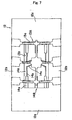
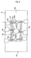
- Figs. 7 and 8 show examples of vibration modes in which the characteristic frequency "fw" of the bonding wire tends to be close to "fd/2".
- the vibration modes shown in Figs. 7 and 8 are relatively complex.
- the characteristic frequency "fw” of such complex vibration mode may be simulated at the time of the initial designing so that the characteristic frequency "fw” is made distant by 10 percent or more from "fd/2". It is thus possible to considerably reduce the zero point temperature drift.
- each bonding wire may be fixed to the substrate 12 at a position near the fixing point of the substrate to an underlying substrate such as a package, so that the above described zero point temperature drift can be further reduced.
- Fig. 9 is a plan view schematically showing a supporting structure according to this embodiment of the present invention.
- the supporting substrate 12 for a vibrator is fixed onto an underlying substrate at predetermined positions, for example six positions 16.
- Each position 16 and each contact point 30 of each bonding wire to the substrate 12 are made close with each other, so that the influences of the vibration of the bonding wire on the detection voltage can be reduced.
- the' distance "L" between the fixing position 16 of the substrate 12 to the underlying substrate and the contact point 30 of the bonding wire to the substrate 12 may preferably be 0.6 mm or smaller and more preferably be 0.4 mm or smaller.
- Fig. 10 is a plan view schematically showing a supporting structure according to still another embodiment of the present invention.
- a bonding wire 16 is formed of bent portions 16a and 16b, and the root of the portion 16b is made distant from a narrower non-fixed portion 12b and made close to X-axis, which is the central axis of the substrate 12.
- X-axis which is the central axis of the substrate 12.
- the protruding part 30 of the bonding wire 16 from the substrate 12 is thus made distant from the narrower portion 12b and made close to the X-axis, so that the influences of the vibration of the substrate 12 on the bonding wire 16 and vibrator 1 can be effectively prevented.
- both ends of a wider portion 12a of the substrate 12 is fixed onto the fixing portion 16.
- the method of fixing is not particularly limited and may be adhesion with a conductive adhesive, welding or the like.
- the vibrator 1, substrate 12 and bonding wires 14A (14B) are contained in a package 19 and a table 17 and an IC chip 18 are mounted thereon.
- the substrate 12 is mounted on the table 17 through the conductive adhesive 16, which is then heated to fix the substrate 12 onto the table 17 by adhesion.
- the kind of the conductive adhesive is not particularly limited, carbon paste and noble metal pastes such as copper, silver, gold paste etc. may be listed.
- the fixed position of the bonding wire onto the substrate and the shape of the bonding wire are not particularly limited.
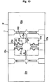
- four bonding wires 21 are protruded from the opposing edges 13b, respectively, and two bonding wires 21 are protruded from the opposing edges 13a, respectively.
- Each bonding wire 21 has straight portions 21a, 21c and a curved portion 21b connecting them.
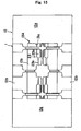
- each of the bonding wires 22A and 22B has substantially the same shape as the bonding wire shown in Fig. 5. According to the present example, however, the width of a central through hole 13B of the substrate 12 is narrower than that shown in Fig. 5 and substantially has a planar shape of a square.
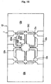
- each bonding wire 23 is extended straightly from opposing edges 13a on the side of wider portions 12a into the through hole 13A.
- Each bonding wire 23 has a wider portion 23a and a narrower portion 23b.
- a supporting structure shown in Fig. 16 is basically the same as the supporting structure shown in Fig. 14.
- the shape of a central through hole 13C is basically rectangular except that curved profiles 13c are formed at the four corners of the rectangular shape, respectively.
- the shape of the through hole may be changed, as described above, to change the length of the bonding wire, so that the characteristic frequency thereof can be changed.
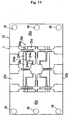
- a wire 24 of a shape of a crank is used instead of the wire 14A having a shape of "L" character shown in Fig. 5.
- the wire 24 has a wider portion 24a, a narrower portion 24b, a bent portion 24c protruding inside from the narrower portion 24b and an additional bent portion 24d.
- the characteristic frequency of vibration of the wire can be changed by increasing the number of bent portions thereof.
- the shape of the central through hole 13C is substantially rectangular except that curved profiles 13c are formed at the four corners of the rectangular shape. Further, short edges 13a and 13d are provided to slightly reduce the length of the bonding wire 24 so that the bonding wire 30 is made slightly longer.
- Each bonding wire 24 having a shape of crank is protruded from the shorter edge 13a and has a wider portion 24a, a narrower portion 24b, a bent portion 24c protruding inside of the narrower portion 24b and an additional bent portion 24d.
- Each straight bonding wire 30 protrudes from the shorter edge 13d and has a wider portion 30a and a narrower portion 30b.
- Fig. 19 is a plan view showing a vibrator whose base portion is supported with six bonding wires shown in Fig. 18.
- each bonding wire may be joined with a terminal portion on the lower face of the vibrator, or, may be joined with a terminal portion on the upper face of the vibrator.
- the dimensions of the vibrator are not particularly limited. However, if the weight or dimensions of the vibrator is too large, too much weight may be applied on the bonding wire to possibly deform the bonding wire over a long period of time.
- the width of the vibrator may preferably be not larger than 10 mm and more preferably be not larger than 5 mm for preventing adverse effects of the deformation of the bonding wire on the vibration.
- the weight of the vibrator may preferably be not larger than 5 mg and more preferably be not larger than 1 mg.
- the thickness of the vibrator may preferably be not larger than 0.3 mm and more preferably be not larger than 0.2 mm.
- the material for the substrate 12 is not particularly limited and may be an insulating material, used for a package, such a ceramics, glass or resin.
- the bonding wire may be joined with the vibrator by means of a process not particularly limited, including bonding by heat pressing, ultrasonic bonding, spot welding, a conductive adhesive or soldering.
- the distance between the vibrator and substrate is not smaller than 0.05 mm and more preferably is not smaller than 0.1 mm.
- the material of the bonding wire is not particularly limited and may be a metal, resin, adhesive or a composite material of a metal and resin, and more preferably be a metal. Copper, gold, aluminum, silver, tungsten, stainless steel, iron, nickel, tin, brass, or the alloys thereof are most preferred. These metals or alloys may be surface treated by plating or the like. For example, copper foil with gold plating is particularly preferred.
- the material of the vibrator is not particularly limited, and may preferably be a piezoelectric single crystal.
- the material may more preferably be a piezoelectric single crystal selected from the group consisting of quartz, lithium niobate, lithium tantalate, lithium niobate-lithium tantalate solid solution, lithium borate and langasite.
- a physical quantity measured according to the present invention is not particularly limited.
- the physical quantity is included in the present invention as far as the physical value can be detected through a detection circuit.
- Such physical quantity may preferably be an acceleration, an angular acceleration or an angular velocity applied on a vibrator.
- the measuring system of the present invention may preferably be an inertia censor.
- the vibrator 1A shown in Figs. 1 and 2 was used. Specifically, a chromium film of 100 angstroms in thickness and a gold film of 1500 angstroms in thickness were formed in predetermined regions on a wafer made of a Z-plate of quartz with a- thickness of 0.1 mm, by sputtering. Both main faces of the wafer were coated with resist films, respectively.
- the wafer was then immersed in aqueous solution of iodine and potassium iodide to remove excessive gold in the gold film by etching, and was further immersed in aqueous solution of cerium-ammonium nitrate and perchloric acid to remove excessive chromium in the chromium film by etching.
- the wafer was etched by immersing the wafer in ammonium bifluoride at a temperature of 80 °C for 20 hours to form the external shape of the vibrator 1.
- a gold film having a thickness of 2000 angstrom is formed as a film for electrode on the chromium film having a thickness of 100 angstrom using a metal mask.
- the vibrator 1 had a length of 2.0 mm, a width of 2.2 mm, a thickness of 0.1 mm and a weight of about 0.3 mg.
- the vibrator 1 was mounted in a package as shown in Fig. 12.
- the substrate 12 was formed of a joined body of a polyimide film and copper foil having a central through hole.
- the copper foil was etched to form the bonding wires, wirings and contact pads on the substrate 12.
- the frame was formed of alumina ceramics.
- the surface of the copper foil was covered with gold plating.
- the bonding wires were joined with the base portion 2 of the vibrator 1 through gold bump 25 by means of bonding by heat pressing.
- each of the bonding wires had a shape shown in Fig. 15 and the width of 0.03 mm.
- the vibrator was supported with six bonding wires.
- the thus obtained vibratory gyroscope was contained in a temperature test bath and the temperature was changed in a range of minus 40 to plus 85 °C.
- the driving vibration was excited using a self oscillation circuit so that the resonance frequency "fd" of the driving vibration mode was changed as shown in table 1. Further, the characteristic frequency "fw" of the bonding wire supporting the vibrator was shown in table 1.
- the thus obtained detection signal was processed to draw a zero point gyroscope signaL It was thus proved that a peak zero point temperature drift was detected in a range of 60 to 85 °C, as shown in Fig. 3.
- the zero point temperature drift was calculated as follows.
- the data of the zero point gyroscope signal was plotted as a function of temperature to provide a graph.
- the graph excluding the peak was approximated by a straight line in a range of minus 40 to plus 85 °C.
- the height of the peak with respect to the straight line was calculated and assigned to the zero poin1 temperature drift.
- the vibrator 1 was supported on the substrate according to the same procedure as the comparative example 1, except that the supporting structure shown in Fig. 17 was applied.
- the numerical values of "fd" and "fw” were shown in table 1.
- the dependency of the zero point gyroscope signal component on temperature was shown in Fig. 4. That is, the zero point gyroscope signal component was gradually lowered substantially according to a linear function between minus 40 to plus 85 °C and a particular zero point temperature drift was not observed.
- the vibrator 1 was supported on the substrate according to the same procedure as the comparative example 1, except that the supporting structure shown in Fig. 15 was applied.
- the numerical values of "fd" and "fw” were shown in table 1.
- a peak of zero point temperature drift was detected in a range of minus 40 to 0 °C, as shown in Fig. 22.
- the temperature drift was considered to be due to resonance of vibration of "2fd”.
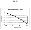
- the amount of drift was considerably reduced compared with that of the comparative example, and the detuning frequency was changed substantially according to a linear function with respect to temperature in a range of minus 40 to plus 85 °C, as shown in Fig. 20.
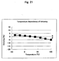
- the vibrator 1 was supported on the substrate according to the same procedure as the comparative example 1, except that the supporting structure shown in Fig. 5 was applied. As a result, a peak of zero point temperature drift was detected as shown in Fig. 23 in a range of 0 °C to 30 °C. The temperature drift is considered to be due to resonance of "3fd". Further, according to the Example 3, the amount of drift was considerably reduced compared with that of the comparative example, and the detuning frequency was gradually changed according to a linear function with respect to temperature in a range of minus 40 to plus 85 °C, as shown in Fig. 21.
- the vibrator 1 was supported on the substrate according to the same procedure as the comparative example 1, except that the supporting structure shown in Fig. 6 was applied.
- the zero point gyroscope signal was gradually changed according to a linear function and the amount of zero point temperature drift was considerably reduced compared with that of the comparative example.
- the vibrator 1 was supported on the substrate according to the same procedure as the comparative example 1, except that the supporting structure shown in Fig. 10 was applied.
- the zero point gyroscope signal was gradually changed according to a linear function and the amount of zero point temperature drift was considerably reduced compared with that of the comparative example.
- a structure for supporting a vibrator 1 is provided.
- the structure comprises a substrate 12 and bonding wires 14A, 14B fixed to the substrate 12 and connected with the vibrator 1.
- the vibrator 1 is supported with the bonding wires so that the vibrator 1 is not directly contacted with the substrate 12.
- "fd” and "fw” satisfy the following formula (1).
- "fd” represents a resonance frequency of a driving vibration mode of the vibrator and "fw” represents a characteristic frequency of a vibration mode of the bonding wire at room temperature.
Landscapes
- Engineering & Computer Science (AREA)
- Physics & Mathematics (AREA)
- General Physics & Mathematics (AREA)
- Radar, Positioning & Navigation (AREA)
- Remote Sensing (AREA)
- Manufacturing & Machinery (AREA)
- Gyroscopes (AREA)
- Measurement Of Mechanical Vibrations Or Ultrasonic Waves (AREA)
Abstract

Description
- This application claims the benefits of Japanese Patent Applications P2005- 207047 filed on July 15, 2005, and P2004- 263310 filed on September 10, 2004, the entireties of which are incorporated by reference.
- The present invention provides a structure for supporting a vibrator and a device for measuring a physical quantity such as a vibratory gyroscope.
- In a vehicle control system, a vibratory gyroscope and its vibrator are subjected to a wide temperature range including high and low temperatures. Such temperature range normally includes minus 40°C to plus 85 °C and may be more wider in a more severe specification. Particularly when a vibrator is made of a piezoelectric single crystal, the temperature dependency of the single crystal may affect the stability of the gyroscope.
- Japanese patent publication 2003-28648A discloses a member for supporting a vibrator for use in a vibratory gyroscope. According to the disclosure, the supporting member is composed of an elongate rod bent in a complex form so that the vibrator is supported with the rod. It is also described that the supporting member is electrically connected with an electrode formed on the vibrator.
- Further, the assignee has filed Japanese patent publication 2003-294450A and disclosed that a vibrator is supported with bonding wires over a substrate in a package. The bonding wires are bonded with electrodes on the surface of the vibrator.
- According to such supporting methods, however, a substantial temperature drift may be observed, for example, in a high temperature region. For example, as shown in Fig. 3, even when the zero point temperature signal is constant in low to room temperature range, the gyroscope signal may be rapidly increased in a range of 60 to 80 °C to result in temperature drift. If the vibrator exhibiting abnormality of oscillation would be used for a vibratory gyroscope, the zero point temperature drift in the detection signal would be increased so that the gyroscope might be inoperative as a sensor in the worst cases.
- An object of the present invention is to provide a supporting structure for a device of measuring a physical quantity using a vibrator for reducing the zero point temperature drift of the detection signal.
- The present invention provides a structure for supporting a vibrator, said structure comprising:
- a substrate; and
- a bonding wire fixed to the substrate and connected with a vibrator;
- wherein the vibrator is supported with the bonding wire so that the vibrator is not directly contacted with said substrate, and wherein "fd" and any "fw" satisfy the following formula (1), provided that "fd" represents a resonance frequency of a driving vibration mode of said vibrator and "fw" represents a characteristic frequency of a vibration mode of the bonding wire at room temperature.

- The present invention further provides a device for measuring a physical quantity comprising the supporting structure described above.
- The inventors have studied the cause of the peak temperature drift, as shown in Fig. 3, and obtained the following findings. That is, it is found that the characteristic vibration frequency "fw" of a bonding wire on a substrate for packaging may be very close to the half of the resonance frequency "fd/2" of the vibration of the driving vibration mode. The driving vibration mode may cause resonance of the bonding wire so as to affect the vibration mode of the vibrator. The resonance may result in the zero point temperature drift of the vibratory gyroscope. It is found that the zero point temperature drift can be reduced by appropriately changing the form of the bonding wire so that °fw" is made distant by a specific ratio from °fd/2".
These and other objects, features and advantages of the invention will be appreciated upon reading the following description of the invention when taken in conjunction with the attached drawings, with the understanding that some modifications, variations and changes of the same could be made by the skilled person in the art. -
- Fig. 1 is a plan view showing the driving vibration mode of a
vibrator 1 usable in the present invention. - Fig. 2 is a plan view showing the detection vibration mode of a
vibrator 1. - Fig. 3 is a graph showing the relationship of the zero point gyro component and temperature in a comparative example.
- Fig. 4 is a graph showing the relationship of the zero point gyro component and temperature in an example according to the present invention.
- Fig. 5 (a) is a plan view schematically showing a supporting structure usable in the present invention.
- Fig. 5 (b) is a front view showing the supporting structure of Fig. 5(a).
- Fig. 6 is a plan view schematically showing a supporting structure according to another embodiment of the present invention.
- Fig. 7 is a plan view of an example of the vibration mode of a bonding wire in the supporting structure shown in Fig. 5.
- Fig. 8 is a plan view of an example of the vibration mode of a bonding wire in the supporting structure shown in Fig. 5.
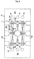
- Fig. 9 is a plan view showing another supporting structure usable for the present invention.
- Fig. 10 is a plan view showing still another supporting structure usable for the present invention:
- Fig. 11 is a plan view showing still another supporting structure usable for the present invention.
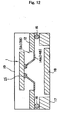
- Fig. 12 is a cross sectional view schematically showing the supporting structure of Fig. 11.
- Fig. 13 is a plan view showing still another supporting structure usable for the present invention.
- Fig. 14 is a plan view showing still another supporting structure usable for the present invention.
- Fig. 15 is a plan view showing still another supporting structure usable for the present invention.
- Fig. 16 is a plan view showing still another supporting structure usable for the present invention.'
- Fig. 17 is a plan view showing still another supporting structure usable for the present invention.
- Fig. 18 is a plan view showing the shapes of a bonding wire and substrate usable for the present invention.
- Fig. 19 is a plan view showing a vibrator supported on the substrate shown in Fig. 18.
- Fig. 20 is a graph showing the temperature change of detuning according to the example of the present invention.
- Fig. 21 is a graph showing the temperature change of detuning according to the example of the present invention.
- Fig. 22 is a chart showing the zero point temperature drift in example 2.
- Fig. 23. is a chart showing the zero point temperature drift in example 3.
- The characteristic frequency "fw" of a bonding wire at room temperature means the characteristic frequency of a certain vibration mode of the bonding wire at 25 °C. "fw" can be measured by means of an impedance analyzer, a system for measuring laser Doppler, or X-ray diffraction topograph Lang camera. A plurality of the vibration modes are normally present for the single bonding wire, so that a plurality of the characteristic frequencies "fw" are present for the corresponding vibration modes, respectively. According to the present invention, it is required that all of the single or plural vibration mode(s) of the bonding wire satisfy the formula (1).
- The resonance frequency °fd" of the driving vibration mode means the characteristic frequency of driving vibration mode excited in a vibrator by a self-oscillation circuit, "fd" can be measured by means of an impedance analyzer.
"fd/2" and "fw" have to satisfy either of the following formulae of (fd/2)×1.05 ≦ f w and fw ≦ (fd/2)×0.95. When "fd/2" and "fw" do not satisfy both of the above formulae, the zero point temperature drift of the detection signal becomes considerable. That is, it has been proved that "fd/2" and "fw" have to be different with each other as described above based on the data of deviation of "fw" and the temperature characteristics of vibrators actually fabricated. - In the formula (1), °fw"may be (fd/2)×1.05 or higher and preferably be (fd/2)×1.10 or higher. Alternatively, °fw" may be (fd/2)×0.95 or lower and preferably be (fd/2)×0.90 or lower.
- According to a preferred embodiment, "fd" and "fw" further satisfy the following formula.

That is, it is required that °2fd" and °fw" satisfy either of °(2fd)×1.03 ≦ f w" and fw ≦ (2fd)×0.97. When "2fd" and "fw" do not satisfy both of the above formulae, the zero point temperature drift of the detection signal becomes considerable. That is, it has been proved that "2fd" and "fw" have to be different with each other as described above based on the data of deviation of "fw" and the temperature characteristics of vibrators actually fabricated.
According to the present embodiment, it is required that all of the single or plural vibration mode(s) of the boding wire satisfy the formula (2).
Moreover, the difference of 0.05 times of (fd/2) between "fd/2" and "fw" was required for reducing the zero point temperature drift of the detection signal in the formula (1). It was further proved that only 0.03 times of (2fd) between "2fd" and "fw" was required for reducing the zero point temperature drift of the detection signal in the formula (2). Such differences of the ratios of the differences necessary for reducing the temperature drift, among the different frequency ranges, were also beyond the expectations of those who skilled in the art. - According to the formula (2), "fw" may be (2fd)×1.03 or higher and preferably be (2fd)×1.05 or higher. Alternatively, "fw" may be (2fd)×0.97 or lower and preferably be (2fd)×0.95 or lower.
- According to a preferred embodiment, °fd" and "fw" further satisfy the following formula (3).

That is, it is required that "3fd" and "fw" satisfy either of "(3fd)×1.05 ≦ fw" and fw ≦ (3fd)×0.95. When "3fd" and "fw" do not satisfy both of the above formulae, the zero point temperature drift of the detection signal becomes considerable. That is, it has been proved that "3fd" and "fw" have to be different with each other, as described above, based on the data of deviation of "fw" and the temperature characteristics of vibrators actually fabricated.
According to the present embodiment, it is required that all of the single or plural vibration mode(s) of the boding wire satisfy the formula (3). - According to the formula (3), "fw" may be (3fd)×1.05 or higher and preferably be (2fd)×1.10 or higher. Alternatively, "fw" may be (2fd)×0.95 or lower and preferably be (2fd)×0.90 or lower.
Although the requirement of the formula (3) gives less considerable influences compared with the requirements of the formulae (1) and (2), it is desirable to further satisfy the requirement of the formula (3) in addition to those of the formulae (1) and (2) for further reducing the temperature drift of the detection signal. - "fd" can be adjusted by changing the material and dimensions of the vibrator. The design of the vibrator is decided depending on various conditions, however, so that it may be impossible to substantially change the material and dimensions of the vibrator. In this case, "fw" is controlled so that each or all of the formulae (1), (2) and (3).
- Although "fw" may be controlled by any method, the followings are listed.
- (1) The diameter, thickness or width of the bonding wire is changed in each of bonding wires.
- (2) The bonding wire is bent.
- (3) The material of a bonding wire is changed.
- (4) The length of a bonding wire is changed.
- According to a preferred embodiment, a vibrator has a driving vibration arm with a driving means provided therein, a detection vibration arm with a detecting means provided therein, and a base portion provided between the driving and detection vibration arms. Preferably, the vibrator further has an elongate connecting portion connecting the base portion and driving vibration arm. Although the present invention will be described referring to the present embodiment, the present invention is not limited to this type of vibrator.
- Fig. 1 is a plan view schematically showing a vibrator 1 (driving vibration mode) according to an embodiment of the present invention. Fig. 2 is a plan view showing the detection vibration mode of the
vibrator 1. - The
vibrator 1 according to the present example has abase portion 2, a pair ofdetection vibration arms base portion 2, a pair of connectingportions 10 each protruding from thebase portion 2, and drivingvibration arms portions 10, respectively. An elongate groove is formed in each of the main faces of the drivingvibration arms vibration arms 4A to 4D substantially has a cross sectional shape of "H" character. A drivingelectrode 9 is formed in the groove. Wide orweight portions vibration arms 4A to 4D, respectively. Throughholes 7 are formed in the wide portions, respectively. - An elongate groove is formed in each of the main faces of the detection'
vibration arms electrode 10 is formed in the groove. Wide orweight portions detection vibration arms holes 8 are formed in the wide portions, respectively. - Fig. 1 shows the driving vibration mode. When driving vibration is excited in the vibrator, each of the driving
vibration arms 4A to 4D vibrates around thebase 11 of the arm to the connectingportion 10 as its fulcrum, as an arrow ''A''. Thevibrator 1 is rotated around a rotating axis (Z-axis) extending in a direction perpendicular to thevibrator 1. The connectingportion 10 then vibrates in bending vibration mode around the base of the connectingportion 10 to the fixing (base)portion 2 as its fulcrum, as an arrow "B". Responsive to the vibration, each of thedetection vibration arms portion 2, as an arrow "C". Each of thedetection vibration arms - Fig. 5 (a) is a plan view schematically showing a supporting structure used for the present invention. Fig. 5(b) is a front view showing a supporting structure of Fig. 5 (a).
- A central through
hole 13A is formed in asubstrate 12. According to the present example, the throughhole 13A has an elongate shape such as a rectangular shape. Thesubstrate 12 haswider portions 12a provided on the both sides of the throughhole 13A andnarrower portions 12b. According to the present example, thewider portion 12a is fixed to a package. Thevibrator 1 is supported direct over the throughhole 13A of thesubstrate 12. According to the present example, the vibrator is supported with fourbonding wires 14A and twobonding wires 14B. Each of the bonding wires protrudes from opposingedges 13a on the side of fixingportion 12a of thesubstrate 12 towards thebase portion 2. - Each of the
bonding wires 14A protrudes from each end of each opposingedge 13a and bent substantially in the planar shape of "L" character. That is, thebonding wire 14A has awider portion 14a formed in a direction substantially parallel with the opposingedge 13b facing the through holes 13, anarrower portion 14b, and abent portion 14c formed in a direction substantially parallel with the opposingedge 13a. The tip end of thebent portion 14c is connected with an electrode formed in thebase portion 2. - Further, two
bonding wires 14B each protruding from the center of each opposingedge 13a has awider portion 14a and anarrower portion 14b. The tip end of thenarrower portion 14b is joined with the fixingportion 2. According to the present example, each of thebonding wires wider portion 14a andnarrower portion 14b, so that the characteristic frequency of the vibration of the whole bonding wire can be controlled. The width of the bonding wire can be easily controlled by, for example, changing the mask width of a mask pattern used for patterning the bonding wire by etching. - According to an example shown in Fig. 6, the width of a through
hole 13B is made narrower than that of the throughhole 13A shown in Fig. 5, so that each bonding wire is made shorter. Such change of the length of the bonding wire results in a change of the characteristic frequency of the vibration of the bonding wire. - According to the present example, two
bonding wires 15 are protruded from each of the opposingedges 13a on the side of thewider portion 12a of thesubstrate 12 towards thebase portion 2. Eachbonding wire 15 has aportion 15a extending in a direction substantially parallel with the opposingedge 13b, and abent portion 15b bent towards the fixingportion 2. The tip end of thebent portion 15b is joined with an electrode on the fixingportion 2. Theportions - Figs. 7 and 8 show examples of vibration modes in which the characteristic frequency "fw" of the bonding wire tends to be close to "fd/2". The vibration modes shown in Figs. 7 and 8 are relatively complex. The characteristic frequency "fw" of such complex vibration mode may be simulated at the time of the initial designing so that the characteristic frequency "fw" is made distant by 10 percent or more from "fd/2". It is thus possible to considerably reduce the zero point temperature drift. These kinds of findings are very useful in the actual design of a vibratory gyroscope.
- Further, each bonding wire may be fixed to the
substrate 12 at a position near the fixing point of the substrate to an underlying substrate such as a package, so that the above described zero point temperature drift can be further reduced. - Fig. 9 is a plan view schematically showing a supporting structure according to this embodiment of the present invention. In Fig. 9, parts already shown in Fig. 5 are represented by the same numerals and the explanation may be omitted. According to the example of Fig. 9, the supporting
substrate 12 for a vibrator is fixed onto an underlying substrate at predetermined positions, for example sixpositions 16. Eachposition 16 and eachcontact point 30 of each bonding wire to thesubstrate 12 are made close with each other, so that the influences of the vibration of the bonding wire on the detection voltage can be reduced. On the viewpoint, the' distance "L" between the fixingposition 16 of thesubstrate 12 to the underlying substrate and thecontact point 30 of the bonding wire to thesubstrate 12 may preferably be 0.6 mm or smaller and more preferably be 0.4 mm or smaller. - Fig. 10 is a plan view schematically showing a supporting structure according to still another embodiment of the present invention.
According to the present example, abonding wire 16 is formed ofbent portions 16a and 16b, and the root of theportion 16b is made distant from a narrowernon-fixed portion 12b and made close to X-axis, which is the central axis of thesubstrate 12. When thesubstrate 12 vibrates, the magnitude of thenon-fixed portion 12b is particularly large. The protrudingpart 30 of thebonding wire 16 from thesubstrate 12 is thus made distant from thenarrower portion 12b and made close to the X-axis, so that the influences of the vibration of thesubstrate 12 on thebonding wire 16 andvibrator 1 can be effectively prevented. - According to an example of Fig. 11, both ends of a
wider portion 12a of thesubstrate 12 is fixed onto the fixingportion 16. The method of fixing is not particularly limited and may be adhesion with a conductive adhesive, welding or the like. Preferably, as schematically shown in Fig. 12, thevibrator 1,substrate 12 andbonding wires 14A (14B) are contained in apackage 19 and a table 17 and anIC chip 18 are mounted thereon. Thesubstrate 12 is mounted on the table 17 through theconductive adhesive 16, which is then heated to fix thesubstrate 12 onto the table 17 by adhesion. - Although the kind of the conductive adhesive is not particularly limited, carbon paste and noble metal pastes such as copper, silver, gold paste etc. may be listed.
- As far as the requirements of the present invention are satisfied, the fixed position of the bonding wire onto the substrate and the shape of the bonding wire are not particularly limited. For example, according to an example shown in Fig. 13, four
bonding wires 21 are protruded from the opposingedges 13b, respectively, and twobonding wires 21 are protruded from the opposingedges 13a, respectively. Eachbonding wire 21 has straight portions 21a, 21c and a curved portion 21b connecting them. - According to an example shown in Fig. 14, each of the
bonding wires hole 13B of thesubstrate 12 is narrower than that shown in Fig. 5 and substantially has a planar shape of a square. - According to an example shown in Fig. 15, for example six
bonding wires 23 are extended straightly from opposingedges 13a on the side ofwider portions 12a into the throughhole 13A. Eachbonding wire 23 has a wider portion 23a and a narrower portion 23b. - A supporting structure shown in Fig. 16 is basically the same as the supporting structure shown in Fig. 14. According to the present example, the shape of a central through
hole 13C is basically rectangular except thatcurved profiles 13c are formed at the four corners of the rectangular shape, respectively. The shape of the through hole may be changed, as described above, to change the length of the bonding wire, so that the characteristic frequency thereof can be changed. - According to an example shown in Fig. 17, a
wire 24 of a shape of a crank is used instead of thewire 14A having a shape of "L" character shown in Fig. 5. Thewire 24 has awider portion 24a, anarrower portion 24b, abent portion 24c protruding inside from thenarrower portion 24b and an additionalbent portion 24d. The characteristic frequency of vibration of the wire can be changed by increasing the number of bent portions thereof. - According to an example of Fig. 18, the shape of the central through
hole 13C is substantially rectangular except thatcurved profiles 13c are formed at the four corners of the rectangular shape. Further,short edges bonding wire 24 so that thebonding wire 30 is made slightly longer. Eachbonding wire 24 having a shape of crank is protruded from theshorter edge 13a and has awider portion 24a, anarrower portion 24b, abent portion 24c protruding inside of thenarrower portion 24b and an additionalbent portion 24d. Eachstraight bonding wire 30 protrudes from theshorter edge 13d and has a wider portion 30a and anarrower portion 30b. - Fig. 19 is a plan view showing a vibrator whose base portion is supported with six bonding wires shown in Fig. 18.
- The end of each bonding wire may be joined with a terminal portion on the lower face of the vibrator, or, may be joined with a terminal portion on the upper face of the vibrator.
- The dimensions of the vibrator are not particularly limited. However, if the weight or dimensions of the vibrator is too large, too much weight may be applied on the bonding wire to possibly deform the bonding wire over a long period of time. The width of the vibrator may preferably be not larger than 10 mm and more preferably be not larger than 5 mm for preventing adverse effects of the deformation of the bonding wire on the vibration. On this viewpoint, the weight of the vibrator may preferably be not larger than 5 mg and more preferably be not larger than 1 mg. Further, the thickness of the vibrator may preferably be not larger than 0.3 mm and more preferably be not larger than 0.2 mm.
- The material for the
substrate 12 is not particularly limited and may be an insulating material, used for a package, such a ceramics, glass or resin. - The bonding wire may be joined with the vibrator by means of a process not particularly limited, including bonding by heat pressing, ultrasonic bonding, spot welding, a conductive adhesive or soldering.
- It is necessary to support the vibrator so that the vibrator does not directly contact the substrate for preventing the adverse effects on the vibration. According to a preferred embodiment, the distance between the vibrator and substrate is not smaller than 0.05 mm and more preferably is not smaller than 0.1 mm.
- The material of the bonding wire is not particularly limited and may be a metal, resin, adhesive or a composite material of a metal and resin, and more preferably be a metal. Copper, gold, aluminum, silver, tungsten, stainless steel, iron, nickel, tin, brass, or the alloys thereof are most preferred.
These metals or alloys may be surface treated by plating or the like. For example, copper foil with gold plating is particularly preferred. - The material of the vibrator is not particularly limited, and may preferably be a piezoelectric single crystal. The material may more preferably be a piezoelectric single crystal selected from the group consisting of quartz, lithium niobate, lithium tantalate, lithium niobate-lithium tantalate solid solution, lithium borate and langasite.
- A physical quantity measured according to the present invention is not particularly limited. When a driving vibration is excited in a vibrator and the vibration state of the vibrator is changed due to the effects of a specific physical quantity exerted on the vibrator, the physical quantity is included in the present invention as far as the physical value can be detected through a detection circuit. Such physical quantity may preferably be an acceleration, an angular acceleration or an angular velocity applied on a vibrator. The measuring system of the present invention may preferably be an inertia censor.
- The vibrator 1A shown in Figs. 1 and 2 was used. Specifically, a chromium film of 100 angstroms in thickness and a gold film of 1500 angstroms in thickness were formed in predetermined regions on a wafer made of a Z-plate of quartz with a- thickness of 0.1 mm, by sputtering. Both main faces of the wafer were coated with resist films, respectively.
- The wafer was then immersed in aqueous solution of iodine and potassium iodide to remove excessive gold in the gold film by etching, and was further immersed in aqueous solution of cerium-ammonium nitrate and perchloric acid to remove excessive chromium in the chromium film by etching. The wafer was etched by immersing the wafer in ammonium bifluoride at a temperature of 80 °C for 20 hours to form the external shape of the
vibrator 1. A gold film having a thickness of 2000 angstrom is formed as a film for electrode on the chromium film having a thickness of 100 angstrom using a metal mask. Thevibrator 1 had a length of 2.0 mm, a width of 2.2 mm, a thickness of 0.1 mm and a weight of about 0.3 mg. - The
vibrator 1 was mounted in a package as shown in Fig. 12. Thesubstrate 12 was formed of a joined body of a polyimide film and copper foil having a central through hole. The copper foil was etched to form the bonding wires, wirings and contact pads on thesubstrate 12. The frame was formed of alumina ceramics. The surface of the copper foil was covered with gold plating. The bonding wires were joined with thebase portion 2 of thevibrator 1 throughgold bump 25 by means of bonding by heat pressing. - According to the present example, each of the bonding wires had a shape shown in Fig. 15 and the width of 0.03 mm. The vibrator was supported with six bonding wires.
- The thus obtained vibratory gyroscope was contained in a temperature test bath and the temperature was changed in a range of
minus 40 to plus 85 °C. The driving vibration was excited using a self oscillation circuit so that the resonance frequency "fd" of the driving vibration mode was changed as shown in table 1. Further, the characteristic frequency "fw" of the bonding wire supporting the vibrator was shown in table 1. - The thus obtained detection signal was processed to draw a zero point gyroscope signaL It was thus proved that a peak zero point temperature drift was detected in a range of 60 to 85 °C, as shown in Fig. 3.
The zero point temperature drift was calculated as follows. The data of the zero point gyroscope signal was plotted as a function of temperature to provide a graph. The graph excluding the peak was approximated by a straight line in a range ofminus 40 to plus 85 °C. The height of the peak with respect to the straight line was calculated and assigned to the zero poin1 temperature drift.Table 1 fd (Hz) Magnitude of (fw) to (fd/2) Magnitude of (fw) to (2fd) Magnitude of (fw) to (3fd) Zero point Tempe rature Drift Figures Comparative Example 1 45000 1.03 0.85 0.88 370 Note 1Example 1 51000 0.71 0.79 0.82 2.5 Fig. 17 Example 2 44800 0.9 0.99 0.93 20 Fig. 15 Example 3 45500 1.16 0.84 1.03 5 Fig. 5 Example 4 50900 0.88 1.24 1.11 4 Fig. 6 Example 5 51100 0.89 1.25 1.19 4 Fig. 10 (Note 1): Fig. 15, Width of bonding wire was uniform and 0.03 mm. - The
vibrator 1 was supported on the substrate according to the same procedure as the comparative example 1, except that the supporting structure shown in Fig. 17 was applied. The numerical values of "fd" and "fw" were shown in table 1. As a result, the dependency of the zero point gyroscope signal component on temperature was shown in Fig. 4. That is, the zero point gyroscope signal component was gradually lowered substantially according to a linear function betweenminus 40 to plus 85 °C and a particular zero point temperature drift was not observed. - The
vibrator 1 was supported on the substrate according to the same procedure as the comparative example 1, except that the supporting structure shown in Fig. 15 was applied. The numerical values of "fd" and "fw" were shown in table 1. As a result, a peak of zero point temperature drift was detected in a range ofminus 40 to 0 °C, as shown in Fig. 22. The temperature drift was considered to be due to resonance of vibration of "2fd". Further, according to the Example 2, the amount of drift was considerably reduced compared with that of the comparative example, and the detuning frequency was changed substantially according to a linear function with respect to temperature in a range ofminus 40 to plus 85 °C, as shown in Fig. 20. - The
vibrator 1 was supported on the substrate according to the same procedure as the comparative example 1, except that the supporting structure shown in Fig. 5 was applied. As a result, a peak of zero point temperature drift was detected as shown in Fig. 23 in a range of 0 °C to 30 °C. The temperature drift is considered to be due to resonance of "3fd". Further, according to the Example 3, the amount of drift was considerably reduced compared with that of the comparative example, and the detuning frequency was gradually changed according to a linear function with respect to temperature in a range ofminus 40 to plus 85 °C, as shown in Fig. 21. - The
vibrator 1 was supported on the substrate according to the same procedure as the comparative example 1, except that the supporting structure shown in Fig. 6 was applied. The zero point gyroscope signal was gradually changed according to a linear function and the amount of zero point temperature drift was considerably reduced compared with that of the comparative example. - The
vibrator 1 was supported on the substrate according to the same procedure as the comparative example 1, except that the supporting structure shown in Fig. 10 was applied. The zero point gyroscope signal was gradually changed according to a linear function and the amount of zero point temperature drift was considerably reduced compared with that of the comparative example.
The present invention has been explained referring to the preferred embodiments, however, the present invention is not limited to the illustrated embodiments which are given by way of examples only, and may be carried out in various modes without departing from the scope of the invention. - A structure for supporting a
vibrator 1 is provided. The structure comprises asubstrate 12 andbonding wires substrate 12 and connected with thevibrator 1. Thevibrator 1 is supported with the bonding wires so that thevibrator 1 is not directly contacted with thesubstrate 12. "fd" and "fw" satisfy the following formula (1). "fd" represents a resonance frequency of a driving vibration mode of the vibrator and "fw" represents a characteristic frequency of a vibration mode of the bonding wire at room temperature.
Claims (5)
- A structure for supporting a vibrator, said structure comprising:a substrate; anda bonding wire fixed to said substrate and connected with said vibrator,
wherein said vibrator is supported with said bonding wire so that said vibrator is not directly contacted with said substrate, and wherein "fd" and "fw" satisfy the following formula (1), provided that "fd" represents a resonance frequency of a driving vibration mode of said vibrator and "fw" represents a characteristic frequency of a vibration mode of said bonding wire at room temperature
- The structure of claim 1, wherein "fd" and °fw" satisfy the following formula (2).

- The structure of claim 1 or 2, wherein "fd" and "fw" satisfy the following formula (3).

- A device for measuring a physical quantity comprising the structure of any one of claims 1 to 3.
- The device of claim 4 comprising a vibratory gyroscope.
Applications Claiming Priority (2)
| Application Number | Priority Date | Filing Date | Title |
|---|---|---|---|
| JP2004263310 | 2004-09-10 | ||
| JP2005207047A JP4381354B2 (en) | 2004-09-10 | 2005-07-15 | Vibrator support structure and physical quantity measuring device |
Publications (3)
| Publication Number | Publication Date |
|---|---|
| EP1635139A2 true EP1635139A2 (en) | 2006-03-15 |
| EP1635139A3 EP1635139A3 (en) | 2010-04-28 |
| EP1635139B1 EP1635139B1 (en) | 2012-10-17 |
Family
ID=35463986
Family Applications (1)
| Application Number | Title | Priority Date | Filing Date |
|---|---|---|---|
| EP05018854A Expired - Lifetime EP1635139B1 (en) | 2004-09-10 | 2005-08-30 | Structures for supporting vibrators and devices for measuring physical quantities using such structures |
Country Status (5)
| Country | Link |
|---|---|
| US (1) | US7334473B2 (en) |
| EP (1) | EP1635139B1 (en) |
| JP (1) | JP4381354B2 (en) |
| KR (2) | KR20060051182A (en) |
| CN (1) | CN1746623B (en) |
Cited By (1)
| Publication number | Priority date | Publication date | Assignee | Title |
|---|---|---|---|---|
| EP1814171A4 (en) * | 2004-10-19 | 2011-02-02 | Seiko Epson Corp | PIEZOELECTRIC DEVICE |
Families Citing this family (14)
| Publication number | Priority date | Publication date | Assignee | Title |
|---|---|---|---|---|
| KR100618342B1 (en) * | 2004-07-29 | 2006-09-04 | 삼성전자주식회사 | Small structure and its manufacturing method |
| JP4924873B2 (en) * | 2006-08-02 | 2012-04-25 | セイコーエプソン株式会社 | Piezoelectric vibration gyro module and piezoelectric vibration gyro sensor |
| DE102006046772A1 (en) * | 2006-09-29 | 2008-04-03 | Siemens Ag | Rotating rate measuring arrangement, has capacitive units formed by fixed electrodes and by other electrodes that are connected with fixed connection, where exciting voltages are supplied to fixed electrodes of capacitive units |
| JP2010190706A (en) * | 2009-02-18 | 2010-09-02 | Panasonic Corp | Inertial force sensor |
| JP5353610B2 (en) * | 2009-09-30 | 2013-11-27 | Tdk株式会社 | Piezoelectric vibration device |
| JP2011220997A (en) * | 2010-03-26 | 2011-11-04 | Seiko Epson Corp | Physical quantity detection element, physical quantity detection device, and electronic device |
| KR101239636B1 (en) * | 2011-04-08 | 2013-03-11 | 국방과학연구소 | Mems resonator, sensor having the same and manufacturing method for mems resonator |
| JP6117467B2 (en) * | 2011-11-04 | 2017-04-19 | セイコーエプソン株式会社 | Manufacturing method of gyro sensor |
| JP6007541B2 (en) | 2012-03-28 | 2016-10-12 | セイコーエプソン株式会社 | Vibrating piece, manufacturing method thereof, gyro sensor, electronic device, and moving body |
| JP6003150B2 (en) * | 2012-03-28 | 2016-10-05 | セイコーエプソン株式会社 | Vibrating piece and gyro sensor, electronic device and moving body |
| JP6074967B2 (en) * | 2012-09-20 | 2017-02-08 | セイコーエプソン株式会社 | Vibrating piece, vibrator, electronic device, electronic device, and moving object |
| JP6318552B2 (en) * | 2013-10-31 | 2018-05-09 | セイコーエプソン株式会社 | Angular velocity sensor, electronic device and moving object |
| EP3737910B1 (en) * | 2018-01-12 | 2022-03-09 | Trimble AB | Geodetic instrument with reduced drift |
| JP7183902B2 (en) | 2019-03-25 | 2022-12-06 | セイコーエプソン株式会社 | Vibration devices, electronic equipment and moving objects |
Citations (2)
| Publication number | Priority date | Publication date | Assignee | Title |
|---|---|---|---|---|
| JP2003028648A (en) | 2001-05-09 | 2003-01-29 | Murata Mfg Co Ltd | Vibrating gyroscope and electronic device using the same |
| JP2003294450A (en) | 2002-01-30 | 2003-10-15 | Ngk Insulators Ltd | Vibrator support device and vibrator support structure |
Family Cites Families (8)
| Publication number | Priority date | Publication date | Assignee | Title |
|---|---|---|---|---|
| US3046423A (en) * | 1958-10-09 | 1962-07-24 | Bliley Electric Company | High shock and vibration resistant piezoelectric crystal units |
| FR2770899B1 (en) * | 1997-11-07 | 1999-12-10 | Commissariat Energie Atomique | VIBRATING MICROGYROMETER |
| JP3206551B2 (en) * | 1998-06-12 | 2001-09-10 | 株式会社村田製作所 | Vibrator and vibrating gyroscope using it |
| JP3767212B2 (en) * | 1998-11-16 | 2006-04-19 | 株式会社村田製作所 | Vibration gyro support structure and support method |
| JP4364349B2 (en) | 1999-07-02 | 2009-11-18 | 日本碍子株式会社 | Vibrating gyroscope |
| JP4305623B2 (en) * | 2002-03-13 | 2009-07-29 | セイコーエプソン株式会社 | Oscillator and vibratory gyroscope |
| US7148609B2 (en) | 2003-05-12 | 2006-12-12 | Ngk Insulators, Ltd. | Structures for supporting vibrators |
| JP4389480B2 (en) * | 2003-05-28 | 2009-12-24 | セイコーエプソン株式会社 | Vibrator support mechanism and vibrator unit |
-
2005
- 2005-07-15 JP JP2005207047A patent/JP4381354B2/en not_active Expired - Lifetime
- 2005-08-29 US US11/214,455 patent/US7334473B2/en not_active Expired - Lifetime
- 2005-08-30 EP EP05018854A patent/EP1635139B1/en not_active Expired - Lifetime
- 2005-09-09 CN CN2005101040153A patent/CN1746623B/en not_active Expired - Lifetime
- 2005-09-09 KR KR1020050084379A patent/KR20060051182A/en not_active Ceased
-
2008
- 2008-07-02 KR KR1020080064106A patent/KR100906178B1/en not_active Expired - Lifetime
Patent Citations (2)
| Publication number | Priority date | Publication date | Assignee | Title |
|---|---|---|---|---|
| JP2003028648A (en) | 2001-05-09 | 2003-01-29 | Murata Mfg Co Ltd | Vibrating gyroscope and electronic device using the same |
| JP2003294450A (en) | 2002-01-30 | 2003-10-15 | Ngk Insulators Ltd | Vibrator support device and vibrator support structure |
Cited By (1)
| Publication number | Priority date | Publication date | Assignee | Title |
|---|---|---|---|---|
| EP1814171A4 (en) * | 2004-10-19 | 2011-02-02 | Seiko Epson Corp | PIEZOELECTRIC DEVICE |
Also Published As
| Publication number | Publication date |
|---|---|
| US20060053883A1 (en) | 2006-03-16 |
| JP4381354B2 (en) | 2009-12-09 |
| KR100906178B1 (en) | 2009-07-03 |
| US7334473B2 (en) | 2008-02-26 |
| CN1746623A (en) | 2006-03-15 |
| KR20080069565A (en) | 2008-07-28 |
| EP1635139B1 (en) | 2012-10-17 |
| JP2006105962A (en) | 2006-04-20 |
| CN1746623B (en) | 2010-07-21 |
| KR20060051182A (en) | 2006-05-19 |
| EP1635139A3 (en) | 2010-04-28 |
Similar Documents
| Publication | Publication Date | Title |
|---|---|---|
| KR100906178B1 (en) | Structures for supporting vibrators and devices for measuring physical quantities | |
| EP2620747A2 (en) | Vibrator and vibratory gyroscope | |
| EP1898180B1 (en) | Vibrators and vibratory gyroscopes | |
| US20030141340A1 (en) | Systems and structures for supporting vibrators | |
| US8434363B2 (en) | Support member of vibrator | |
| US7278313B2 (en) | Structures for supporting vibrators and devices for measuring physical quantities | |
| EP1496337B1 (en) | Vibratory gyroscope with structures for supporting the vibrator | |
| JP4859347B2 (en) | Vibrating gyroscope | |
| JP2004333416A (en) | Apparatus for measuring physical quantity | |
| JP2004309443A (en) | Vibrator support structure | |
| JP2003315047A (en) | Vibrator electrical connection structure and vibratory gyroscope | |
| JP2004317387A (en) | Physical quantity measuring device | |
| JP2008058049A (en) | Vibrator, and vibration type gyroscope using vibrator | |
| JP2005156457A (en) | Oscillator, electronic device, and measuring device for physical quantities |
Legal Events
| Date | Code | Title | Description |
|---|---|---|---|
| PUAI | Public reference made under article 153(3) epc to a published international application that has entered the european phase |
Free format text: ORIGINAL CODE: 0009012 |
|
| AK | Designated contracting states |
Kind code of ref document: A2 Designated state(s): AT BE BG CH CY CZ DE DK EE ES FI FR GB GR HU IE IS IT LI LT LU LV MC NL PL PT RO SE SI SK TR |
|
| AX | Request for extension of the european patent |
Extension state: AL BA HR MK YU |
|
| RAP1 | Party data changed (applicant data changed or rights of an application transferred) |
Owner name: SEIKO EPSON CORPORATION |
|
| PUAL | Search report despatched |
Free format text: ORIGINAL CODE: 0009013 |
|
| AK | Designated contracting states |
Kind code of ref document: A3 Designated state(s): AT BE BG CH CY CZ DE DK EE ES FI FR GB GR HU IE IS IT LI LT LU LV MC NL PL PT RO SE SI SK TR |
|
| AX | Request for extension of the european patent |
Extension state: AL BA HR MK YU |
|
| RIC1 | Information provided on ipc code assigned before grant |
Ipc: G01C 19/56 20060101AFI20051227BHEP Ipc: H03H 9/09 20060101ALI20100324BHEP |
|
| 17P | Request for examination filed |
Effective date: 20100630 |
|
| 17Q | First examination report despatched |
Effective date: 20100729 |
|
| AKX | Designation fees paid |
Designated state(s): DE FR GB |
|
| GRAJ | Information related to disapproval of communication of intention to grant by the applicant or resumption of examination proceedings by the epo deleted |
Free format text: ORIGINAL CODE: EPIDOSDIGR1 |
|
| GRAP | Despatch of communication of intention to grant a patent |
Free format text: ORIGINAL CODE: EPIDOSNIGR1 |
|
| GRAP | Despatch of communication of intention to grant a patent |
Free format text: ORIGINAL CODE: EPIDOSNIGR1 |
|
| GRAS | Grant fee paid |
Free format text: ORIGINAL CODE: EPIDOSNIGR3 |
|
| GRAA | (expected) grant |
Free format text: ORIGINAL CODE: 0009210 |
|
| AK | Designated contracting states |
Kind code of ref document: B1 Designated state(s): DE FR GB |
|
| REG | Reference to a national code |
Ref country code: GB Ref legal event code: FG4D Ref country code: DE Ref legal event code: R081 Ref document number: 602005036545 Country of ref document: DE Owner name: SEIKO EPSON CORPORATION, JP Free format text: FORMER OWNERS: NGK INSULATORS, LTD., NAGOYA-SHI, AICHI-KEN, JP; SEIKO EPSON CORP., TOKYO, JP |
|
| REG | Reference to a national code |
Ref country code: DE Ref legal event code: R096 Ref document number: 602005036545 Country of ref document: DE Effective date: 20121213 |
|
| PLBE | No opposition filed within time limit |
Free format text: ORIGINAL CODE: 0009261 |
|
| STAA | Information on the status of an ep patent application or granted ep patent |
Free format text: STATUS: NO OPPOSITION FILED WITHIN TIME LIMIT |
|
| 26N | No opposition filed |
Effective date: 20130718 |
|
| REG | Reference to a national code |
Ref country code: DE Ref legal event code: R097 Ref document number: 602005036545 Country of ref document: DE Effective date: 20130718 |
|
| GBPC | Gb: european patent ceased through non-payment of renewal fee |
Effective date: 20130830 |
|
| REG | Reference to a national code |
Ref country code: FR Ref legal event code: ST Effective date: 20140430 |
|
| PG25 | Lapsed in a contracting state [announced via postgrant information from national office to epo] |
Ref country code: GB Free format text: LAPSE BECAUSE OF NON-PAYMENT OF DUE FEES Effective date: 20130830 |
|
| PG25 | Lapsed in a contracting state [announced via postgrant information from national office to epo] |
Ref country code: FR Free format text: LAPSE BECAUSE OF NON-PAYMENT OF DUE FEES Effective date: 20130902 |
|
| PGFP | Annual fee paid to national office [announced via postgrant information from national office to epo] |
Ref country code: DE Payment date: 20240702 Year of fee payment: 20 |
|
| REG | Reference to a national code |
Ref country code: DE Ref legal event code: R071 Ref document number: 602005036545 Country of ref document: DE |