EP1632847A2 - Procédé et appareil de gestion de mémoire pendant le traitement d' instructions - Google Patents
Procédé et appareil de gestion de mémoire pendant le traitement d' instructions Download PDFInfo
- Publication number
- EP1632847A2 EP1632847A2 EP05108040A EP05108040A EP1632847A2 EP 1632847 A2 EP1632847 A2 EP 1632847A2 EP 05108040 A EP05108040 A EP 05108040A EP 05108040 A EP05108040 A EP 05108040A EP 1632847 A2 EP1632847 A2 EP 1632847A2
- Authority
- EP
- European Patent Office
- Prior art keywords
- storage
- instructions
- processing
- estimate
- procedure
- Prior art date
- Legal status (The legal status is an assumption and is not a legal conclusion. Google has not performed a legal analysis and makes no representation as to the accuracy of the status listed.)
- Withdrawn
Links
Images



Classifications
-
- G—PHYSICS
- G06—COMPUTING OR CALCULATING; COUNTING
- G06F—ELECTRIC DIGITAL DATA PROCESSING
- G06F9/00—Arrangements for program control, e.g. control units
- G06F9/06—Arrangements for program control, e.g. control units using stored programs, i.e. using an internal store of processing equipment to receive or retain programs
- G06F9/30—Arrangements for executing machine instructions, e.g. instruction decode
- G06F9/30003—Arrangements for executing specific machine instructions
- G06F9/30076—Arrangements for executing specific machine instructions to perform miscellaneous control operations, e.g. NOP
-
- G—PHYSICS
- G06—COMPUTING OR CALCULATING; COUNTING
- G06F—ELECTRIC DIGITAL DATA PROCESSING
- G06F9/00—Arrangements for program control, e.g. control units
- G06F9/06—Arrangements for program control, e.g. control units using stored programs, i.e. using an internal store of processing equipment to receive or retain programs
- G06F9/30—Arrangements for executing machine instructions, e.g. instruction decode
- G06F9/30098—Register arrangements
-
- G—PHYSICS
- G06—COMPUTING OR CALCULATING; COUNTING
- G06F—ELECTRIC DIGITAL DATA PROCESSING
- G06F12/00—Accessing, addressing or allocating within memory systems or architectures
-
- G—PHYSICS
- G06—COMPUTING OR CALCULATING; COUNTING
- G06F—ELECTRIC DIGITAL DATA PROCESSING
- G06F9/00—Arrangements for program control, e.g. control units
- G06F9/06—Arrangements for program control, e.g. control units using stored programs, i.e. using an internal store of processing equipment to receive or retain programs
- G06F9/30—Arrangements for executing machine instructions, e.g. instruction decode
- G06F9/30098—Register arrangements
- G06F9/3012—Organisation of register space, e.g. banked or distributed register file
- G06F9/30134—Register stacks; shift registers
Definitions
- the present invention relates to a method for managing storage used by a processor when processing instructions. More particularly, but not exclusively, the present invention relates to managing registers used by the processor to improve the performance of the processor.
- Computer processors use a primary storage facility to store the results of processed instructions and to pass data from one instruction to another.
- the primary storage reduces execution time of a program by providing immediate storage for the data being processed thus avoiding any delay in transferring the data to and from memory.
- the primary storage In the ItaniumTM architecture, for example, the primary storage is referred to as a Register Stack and in the Sun SPARCTM architecture the primary storage is referred to as a Register Window.
- register stacks are fmite in size and as a result, as call depth increases during the execution of a set of instructions the processor needs to save the data in some of the registers in a secondary storage facility or memory. Saving register contents to memory frees up registers for the processing of subsequent sets of instructions or procedure/function calls.
- the SPARCTM architecture generates a trigger in the software called a trap to initiate the saving of registers to create free registers. This method works well when the call depths are shallow or when the program depth does not change significantly to cause register window overflow. Traps are however computationally expensive as outlined in 64-bit CPUs: Alpha, SPARC, MIPS and Power, by Jim Turley, February 21, 2002.
- the ItaniumTM architecture avoids the use of traps by employing a Register Save Engine (RSE) which automatically saves registers to memory.
- RSE Register Save Engine
- the RSE can operate in two alternative modes. In the first mode is called the lazy mode and in this mode only a new stack frame allocation triggers the RSE to save registers to memory. The second mode is called the eager and in this mode registers are saved as and when the memory bus is idle.
- the register saves/restores in eager mode can occur any time, not necessarily during the procedure entry and exit.
- the modes of operation of the ItaniumTM RSE each have drawbacks in different scenarios. Given a register stack with more free registers than are required to complete the execution of the procedure sequence, the processor would not be required to perform any register stack saves (or restores). However, if the RSE mode of operation is set to eager, the processor will aggressively pursue saving and loading back registers across the procedure call/returns, resulting unnecessary memory traffic. If the RSE operation was set to lazy mode, and program execution requires more registers then are free, the operation of the RSE may stall the execution of the program whenever a procedure's register requirement exceeds the available clean registers in the register stack.
- a method for managing storage used by a processor when processing instructions comprising the steps of:
- step d) the transferring of data is performed whenever a communications path to the secondary storage is not in use.
- the method further comprises the step of: f) if the free storage is greater than or equal to the required storage then only transferring data from the primary storage to a secondary storage facility when the primary storage facility reaches a predetermined limit.
- the storage used for the processing of a given set of instructions is recorded in a storage record associated with the set of instructions and the storage record is used to provide the storage estimate for a subsequent processing of the given set of instructions.
- the storage record is updated with the storage used for each subsequent processing of the given set of instructions.
- a plurality of storage estimates are provided, each the storage estimate being associated with a set of instructions.
- the storage estimate is provided by one of the set of instructions.
- the storage estimate is generated during compilation of the set of instructions from source code.
- the storage estimate is generated from a call graph for the source code.
- the storage estimate is inserted into the set of instructions during the compilation of the source code.
- the storage estimate is determined during linking of object code for the set of instructions.
- the primary storage is a register stack frame and the set of instructions are assembly code instructions representing a procedure or function call.
- the processor is and ItaniumTM processor and the transferring of data to the secondary storage is carried out by a register stack engine.
- the register stack engine is switched to eager mode to carry out the transferring of data in step d).
- an apparatus for managing storage used by a processor when processing instructions comprising:
- a computer program or set of computer programs arranged to cause a computer to carry out a method for managing storage used by a processor when processing instructions, the method comprising the steps of:
- a computer program or set of computer programs arranged to enable a computer to provide an apparatus for managing storage used by a processor when processing instructions, the apparatus comprising:
- processor comprising:
- a sixth aspect of the invention there is provided a method of controlling the register stack engine in a processor, the method comprising the steps of:
- a seventh aspect of the invention there is provided a method of compiling a program from source code to object code for use by a processor, the method comprising the steps of:
- FIG. 1 shows a computer processor 101 in the form of an ItaniumTM processor.
- the processor 101 has a central processing unit (CPU) 103 indicated in figure 1 by a broken line.
- the CPU 103 is made up of a number of sub-units and is connected to a memory 105 via an instruction cache 107 and a data cache 109.
- the instruction cache is connected to an instruction decode and control unit (IDCU) 111 in the CPU 103 which in turn is connected to a branch prediction and control unit (BPCU) 113.
- the BPCU 113 is connected to an arithmetic logic unit and floating point unit (ALU/FPU) 115 which includes branch units and is, in turn, in communication with a register bank 117.
- ALU/FPU arithmetic logic unit and floating point unit
- the register bank 117 is in communication with a register save engine (RSE) 119 and also connected to an RSE mode control and renaming logic unit (RMC) 121. Both the RSE 119 and the register bank 117 are in communication with the data cache 109.
- RSE register save engine
- RMC RSE mode control and renaming logic unit
- the memory 105 is addressable and accessible by the CPU 103. All memory accesses by the CPU 103 are routed through the instruction cache 109 or the data cache 109 to improve program execution time.
- the IDCU 111 fetches instructions for the processor that are stored in the memory 105 via the instruction cache 107 and then decodes the instruction and passes information/actions as appropriate to the other sub-units of the CPU 103.
- the BPCU 113 analyses instructions destined for the ALU 103 to predict the likelihood of a branch instruction being taken by the instruction stream and provides this data to the branch units in the ALU/FPU 115.
- the ALU/FPU 115 processes received instructions and in doing so access the registers in the register bank 117 to store and retrieve data.
- the register bank 117 is the complete physical register bank for the CPU 103.
- the RMC 121 manages the use of the register bank 117 by the ALU 115 and in doing so controls which registers are architecturally visible to a current instruction stream.
- the RMC allocates and de-allocates groups of registers which are associated with a set of instructions being processed. Such groups of registers are referred to as stack frames.
- the RMC 121 also controls the mode of operation of the RSE 119 which stores and loads the contents of the registers to and from the memory 105 as a background operation.
- the RSE 119 operates in one of two modes referred to as a lazy mode and an eager mode.
- the lazy mode the RSE waits for new stack frame to be allocated by the RMC 121 before it stores the contents of registers to the memory 105.
- the RSE 119 restores or loads the contents of the registers that belong to the previous stack frame from memory if required.
- eager mode the RSE 119 will attempt to perform loads and stores between the memory 105 and the register bank 117 whenever the communications link between them, that is the memory bus, is idle.
- Figure 2 is a call graph for a segment of a program (not shown) which maps procedures or function calls within the program segment.
- the call graph shows that a main program segment 201 calls a procedure A 203 which in turn may invoke a procedure D 205, a procedure B 207 or a procedure C 211.
- the procedure B 207 may in turn invoke a procedure E and the procedure C 211 may in turn invoke a procedure F 213.
- the numbers in brackets in each procedure shown in figure 2 indicate the registers used by each procedure.
- the numbers along the arcs indicate the maximum number of registers used by the procedures represented by the nodes below the arc.
- Minimum Usage ( P ) Own Usage ( P ) + Minimum Usage ( descendants of P )
- the RMC 121 monitors the usage of the register bank during the processing of instructions by the CPU 103.
- the RMC maintains the following ordered lists:
- the compiler determines the number of registers required for a given procedure or function call.
- the compiler enters an instruction called an alloc instruction at the start of the object code for each procedure or function call which defines the register requirements for that procedure or function.
- the alloc instruction is executed and the appropriate stack frame size allocated to that procedure.
- the RMC 121 1 updates the Dynamic Maximum Register Usage list with the stack frame size resulting from the alloc instruction.
- the Required Register Estimate is updated with the value for that procedure from the Dynamic Maximum Register Usage list.
- each of the three lists described above has forty entries.
- data can be held for forty procedures or functions. If more than forty procedures are encountered in the processing of a program the RMC 121 is arranged to replace the oldest entry in each of the lists with entries for each new procedure as and when the new procedures are encountered.
- the RMC 121 carries out two tasks effectively in parallel. Firstly, the RMC begins the maintenance of the three lists noted above to create the entries in the RRE list as noted above. Secondly, the RMC inspects the RRE list for an existing entry for the procedure being entered.
- the RMC 121 retrieves the associated value and uses it to control the operation of the RSE 119.
- the RMC uses the value from the RRE as an estimate of the register usage for the procedure and compares this to the number of free registers in the register bank. If, according to the estimate, there are fewer free registers than are needed for the current procedure and its callees, the RMC instructs the RSE to continue in its default eager mode. If there are more free registers than are needed for the current procedure and its callees according to the estimate then the RMC instructs the RSE to switch modes to the lazy mode. In this way, the RMC controls the mode of the RSE so that it operates in its lazy mode whenever appropriate.
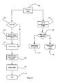
- the performance of the RMC 121 when a program being processed enters a procedure is set out in the flow chart of figure 3.
- the procedure entry is detected by the RMC and two parallel streams of processing are initiated.
- the first process moves to step 303 where a check is carried out to establish is the CCD list is full, in other words has more than forty entries. If the CCD is not full then processing moves to step 307. If the CCD list is full then processing moves to step 305 where the oldest entry from both the CCD and DMRU lists are removed and processing moves to step 307.
- the CCD list is updated with an entry holding the number of registers allocated to the procedure being processed and at step 309 the entries for each ancestor of the new entry have the new value added to their entries.
- Processing then moves to step 311 where the DMRU list has an entry added which includes the name of the procedure and the register allocation for the new procedure.
- each ancestors entry is updated with the maximum register value in the DMRU list and the corresponding entry in the CCD. In other words, if the value for a given procedure in the CCD list is higher than the corresponding value in the DMRU list then the DMRU list entry is update with the value from the CCD list entry. In this manner, the maximum register usage for any given procedure being processed in recorded in the DMRU list. Processing then ends at step 313.
- the second stream of processing on procedure entry takes processing to step 315 at which the RMC 121 looks up the procedure's name in the RRE list and if present retrieves the register usage estimate. Processing then moves to step 317 at which the register usage estimate is compared to the current number of free registers in the register bank 117. If the number of free registers is greater than the register usage estimate then processing moves to step 319 where the mode of the RSE 119 is maintained in the default, eager mode. If however the number of free registers is more than the required register estimate then processing moves to step 321 where the mode of the RSE 119 is switched from the default mode to lazy mode.
- step 401 The performance of the RMC 121 when a program being processed exits a procedure is set out in the flow chart of figure 4.
- step 401 the procedure exit is detected by the RMC and processing moves to step 403 where the DMRU list entry for the procedure is placed in the RRE list either as a new entry if this is the first processing of the procedure or as an update to an existing entry for the procedure.
- step 405 each entry in the CCD list is decremented by the value in that list for the current procedure and processing moves to step 407.
- step 407 the entries in the DMRU and CCD lists for the exiting procedure are removed and at step 409 the process ends.
- the system described above provides an estimate of the number of register stack registers required by each routine.
- the run time computed register usage values are stored and can be looked-up or updated for a given routine.
- the RMC looks-up the entry for the procedure. If an entry is found, the value of depth stored is compared with the number of free registers available. If sufficient registers are free, the back-in-store operation of the RSE engine will be switched to lazy mode. If no entry is found for the given procedure, the RSE will continue to operate in its default eager mode. Given that most programs spent 80% of their execution time in 20% of their code a small RRE list is usually sufficient to store the most recent procedures or functions executed by a program and aid in switching the operation mode of the RSE. The size of the RRE list may be varied and can be determined from empirical analysis or simulations.
- the estimate is created statically during the compilation, loading and linking process of the source code into object code.
- the compiler, linker and loader programs operate to estimate register usage for each procedure or function in the program and to insert special instructions called RSE hint instructions into the object code.
- the RSE hint instructions are processed at run time and used by the RMC to control the mode of the RSE appropriately.
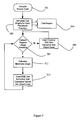
- step 501 the compilation process is initiated and processing moves to step 503 where the compiler creates a call graph 505 covering each procedure or function in the source code.
- the call graph may be represented in the form of a directed acyclic graph.
- Figure 2 shows a call graph for a program in which the main program segment 201 calls procedure A 203 which in turn may invoke procedure D 205, procedure B 207 or procedure C 211.
- Procedure B 207 may in turn invoke procedure E and procedure C 211 may in turn invoke procedure F 213.
- step 507 a check is carried out to establish whether or not register usage is available for each procedure in turn. If a procedure/function that make calls to procedures/functions whose register usage details are not available at the program compile time, processing moves to step 509 where the compiler generates a dummy RSE hint instruction into the object code being generated.
- the register usage details may not be present, for example, where a call is made to a library procedure which may be statically or dynamically linked.
- the dummy RSE hint instruction is used by the linker and loader programs that later process the object code to insert real RSE hint instructions when the register usage details for the relevant procedure or function become available. Once a dummy RSE hint instruction has been inserted processing returns to step 507 to process the next procedure or function.
- step 507 If at step 507 all callee's register usage data is available then processing then moves to step 511 where, for each procedure P in the call graph the maximum register usage is calculated.
- the calculation is the sum of the register usage applied to the given procedure P and the maximum usage of each procedure or function that is called from within the procedure P, that is, the maximum usage of the callees of procedure P.
- the numbers in brackets in each procedure indicate the registers used by each procedure as calculated by the compiler.
- the numbers along the arcs indicate the maximum number of registers used by the procedures represented by the nodes below the arc as calculated using the formula above.
- Step 513 the RSE hint instruction including the register usage estimate is inserted into the object code for the procedure or function being processed. Processing then returns to step 507 where the next procedure or function is processed as described above. Processing continues until all procedures and function in the object code have been processed and either dummy or real RSE hint instructions inserted into their corresponding object code.
- the linker/loader program can patch the compiler generated dummy RSE hint instructions when the correct register usage data is available before the program begins to execute.
- the linker/loader will only patch the RSE hint instructions that the compiler has explicitly left to be patched. If the compiler and the linker/loader are unable to determine the register usage for a procedure then the dummy RSE hint instruction is left in the code.
- the dummy RSE instruction carries a register usage value of minus one.
- An example of when register usage may not be determinable prior to execution is when a procedure or function is recursive. Such recursion can be identified by cycles in the call graph. The same technique is applied when dynamic (pointer based) calls are encountered by the compiler or linker/loader programs.
- the RSE hint instruction is inserted into the object code.
- the CPU 103 is arranged in the present embodiment to include RSE hint instructions in its instruction set.
- the RMC 121 controls the mode of operation of the RSE 119.
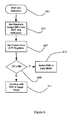
- the processing of the RSE hint instruction is illustrated in the flow chart of figure 6 in which at step 602 the RSE hint instruction is identified and processing moves to step 603.
- the maximum register usage is extracted from the instruction and processing moves to step 607 where the number of free registers in the register bank 117 is retrieved.
- processing then moves to step 609 where the number of currently free registers is compared to the maximum register usage. If the number of free registers is less than the maximum register usage then processing moves to step 611 where the RSE is left to continue in its default, eager mode of operation. If at step 609 the number of current free registers is more than the maximum register usage then processing moves to step 613 where the RSE is switched to its lazy mode of operation.
- the procedure or function exits or returns the RMC 121 switches the RSE back to its eager mode as the default.
- the mode of the RSE engine remains unchanged.
- the compiler in step 511 calculates the maximum register usage of each procedure or function in the program being compiled.
- the compiler performs in the same manner as described above with reference to figure 5 except that instead it calculates the minimum register usage for each procedure or function and inserts this value into the RSE hint instruction in the object code.
- the calculation is the sum of the register usage applied to the given procedure P and the minimum usage of each procedure or function that is called from within the procedure P, that is, the minimum usage of the callees of procedure P.
- the RMC in this alternative embodiment is arranged to operate in the same manner as described above with reference to figure 6 except that in steps 603 and 609 the minimum register usage is used instead of the maximum register usage.
- both the maximum and minimum register usage are calculated by the compiler and inserted into the RSE hint instruction in the object code.
- the invention is performed in the context of the ItaniumTM architecture which implements a register save engine to manage the register bank.
- the CPU may use other mechanisms to manage the storage that is used in the processing of instructions.
- any storage used by the CPU need not be on-chip registers as is the case with ItaniumTM but may be any other suitable storage facility or combination thereof.
- Primary storage refers to the storage facility which provides the immediate storage for the CPU during its processing of instructions.
- secondary storage refers to the storage used to provide space for saving the contents of primary storage and is addressable by the address space of the CPU. The physical location of the primary and secondary storage is dependent on a particular implementation. Either storage facility may be provided by registers or by memory, either locally to the CPU or remote from it.
- the apparatus that embodies a part or all of the present invention may be a general purpose device having software arranged to provide a part or all of an embodiment of the invention.
- the device could be single device or a group of devices and the software could be a single program or a set of programs.
- any or all of the software used to implement the invention can be communicated via various transmission or storage means such as computer network, floppy disc, CD-ROM or magnetic tape so that the software can be loaded onto one or more devices.
Landscapes
- Engineering & Computer Science (AREA)
- Theoretical Computer Science (AREA)
- Software Systems (AREA)
- Physics & Mathematics (AREA)
- General Engineering & Computer Science (AREA)
- General Physics & Mathematics (AREA)
- Devices For Executing Special Programs (AREA)
- Memory System Of A Hierarchy Structure (AREA)
Applications Claiming Priority (1)
| Application Number | Priority Date | Filing Date | Title |
|---|---|---|---|
| GB0419421A GB2417797B (en) | 2004-09-02 | 2004-09-02 | A method and apparatus for managing storage used by a processor when processing instructions |
Publications (2)
| Publication Number | Publication Date |
|---|---|
| EP1632847A2 true EP1632847A2 (fr) | 2006-03-08 |
| EP1632847A3 EP1632847A3 (fr) | 2008-02-20 |
Family
ID=33155862
Family Applications (1)
| Application Number | Title | Priority Date | Filing Date |
|---|---|---|---|
| EP05108040A Withdrawn EP1632847A3 (fr) | 2004-09-02 | 2005-09-02 | Procédé et appareil de gestion de mémoire pendant le traitement d' instructions |
Country Status (3)
| Country | Link |
|---|---|
| US (1) | US7698525B2 (fr) |
| EP (1) | EP1632847A3 (fr) |
| GB (1) | GB2417797B (fr) |
Families Citing this family (5)
| Publication number | Priority date | Publication date | Assignee | Title |
|---|---|---|---|---|
| US7962731B2 (en) * | 2005-10-20 | 2011-06-14 | Qualcomm Incorporated | Backing store buffer for the register save engine of a stacked register file |
| US7844804B2 (en) * | 2005-11-10 | 2010-11-30 | Qualcomm Incorporated | Expansion of a stacked register file using shadow registers |
| US8310298B2 (en) * | 2006-09-20 | 2012-11-13 | International Business Machines Corporation | Ratioed feedback body voltage bias generator |
| US20100131803A1 (en) * | 2008-11-25 | 2010-05-27 | Express Logic | Computation of stack usage in embedded computing systems |
| US8614599B1 (en) * | 2010-12-08 | 2013-12-24 | Xilinx, Inc. | Method and apparatus for powering down a dual supply current source |
Family Cites Families (18)
| Publication number | Priority date | Publication date | Assignee | Title |
|---|---|---|---|---|
| US5235690A (en) * | 1990-08-31 | 1993-08-10 | International Business Machines Corporation | Method for operating a cached peripheral data storage subsystem including a step of subsetting the data transfer into subsets of data records |
| JPH0659982A (ja) * | 1992-08-10 | 1994-03-04 | Hitachi Ltd | 仮想記憶制御方法および装置 |
| US5602749A (en) * | 1995-01-12 | 1997-02-11 | Mtc | Method of data compression and apparatus for its use in monitoring machinery |
| US6230173B1 (en) * | 1995-07-17 | 2001-05-08 | Microsoft Corporation | Method for creating structured documents in a publishing system |
| IL117133A (en) * | 1996-02-14 | 1999-07-14 | Olivr Corp Ltd | Method and system for providing on-line virtual reality movies |
| US6225993B1 (en) * | 1996-04-22 | 2001-05-01 | Sun Microsystems, Inc. | Video on demand applet method and apparatus for inclusion of motion video in multimedia documents |
| US6370543B2 (en) * | 1996-05-24 | 2002-04-09 | Magnifi, Inc. | Display of media previews |
| US6564383B1 (en) * | 1997-04-14 | 2003-05-13 | International Business Machines Corporation | Method and system for interactively capturing organizing and presenting information generated from television programs to viewers |
| US6279016B1 (en) * | 1997-09-21 | 2001-08-21 | Microsoft Corporation | Standardized filtering control techniques |
| JPH1196175A (ja) * | 1997-09-22 | 1999-04-09 | Nec Corp | データベース検索表示方法および検索方式 |
| US6738678B1 (en) * | 1998-01-15 | 2004-05-18 | Krishna Asur Bharat | Method for ranking hyperlinked pages using content and connectivity analysis |
| US6219783B1 (en) | 1998-04-21 | 2001-04-17 | Idea Corporation | Method and apparatus for executing a flush RS instruction to synchronize a register stack with instructions executed by a processor |
| US6487630B2 (en) * | 1999-02-26 | 2002-11-26 | Intel Corporation | Processor with register stack engine that dynamically spills/fills physical registers to backing store |
| US6360364B1 (en) * | 1999-03-17 | 2002-03-19 | Microsoft Corporation | System and method for installing an application on a portable computer |
| JP3707991B2 (ja) * | 2000-04-12 | 2005-10-19 | シャープ株式会社 | 通信装置及び方法並びにこれに利用される記憶媒体 |
| WO2003009144A1 (fr) * | 2001-07-19 | 2003-01-30 | Wind River Systems, Inc. | Systeme de gestion memoire |
| US9087319B2 (en) * | 2002-03-11 | 2015-07-21 | Oracle America, Inc. | System and method for designing, developing and implementing internet service provider architectures |
| US7120775B2 (en) * | 2003-12-29 | 2006-10-10 | Intel Corporation | Inter-procedural allocation of stacked registers for a processor |
-
2004
- 2004-09-02 GB GB0419421A patent/GB2417797B/en not_active Expired - Fee Related
-
2005
- 2005-09-01 US US11/219,048 patent/US7698525B2/en not_active Expired - Fee Related
- 2005-09-02 EP EP05108040A patent/EP1632847A3/fr not_active Withdrawn
Also Published As
| Publication number | Publication date |
|---|---|
| GB2417797B (en) | 2009-05-13 |
| US7698525B2 (en) | 2010-04-13 |
| GB0419421D0 (en) | 2004-10-06 |
| GB2417797A (en) | 2006-03-08 |
| EP1632847A3 (fr) | 2008-02-20 |
| US20060047921A1 (en) | 2006-03-02 |
Similar Documents
| Publication | Publication Date | Title |
|---|---|---|
| JP3311462B2 (ja) | コンパイル処理装置 | |
| JP3820261B2 (ja) | データ処理システムの外部および内部命令セット | |
| US6065115A (en) | Processor and method for speculatively executing instructions from multiple instruction streams indicated by a branch instruction | |
| US5872985A (en) | Switching multi-context processor and method overcoming pipeline vacancies | |
| EP1570352B1 (fr) | Mecanisme de virtualisation de processeur au moyen d'une restauration amelioree d'etats a architecture dure | |
| US5944817A (en) | Method and apparatus for implementing a set-associative branch target buffer | |
| US20110060889A1 (en) | Method, system and computer-accessible medium for providing a distributed predicate prediction | |
| KR100310900B1 (ko) | 파이프라인동기를사용하여마이크로프로세서를개선시키는방법 | |
| US20040168078A1 (en) | Apparatus, system and method for protecting function return address | |
| US11036511B2 (en) | Processing of a temporary-register-using instruction including determining whether to process a register move micro-operation for transferring data from a first register file to a second register file based on whether a temporary variable is still available in the second register file | |
| JP2007507048A (ja) | マルチスレッディングのためのコンパイラが生成したヘルパースレッドの方法および装置 | |
| EP0638183A1 (fr) | Systeme et procede permettant d'annuler des instructions dans un microprocesseur superscalaire. | |
| JPH096633A (ja) | データ処理システムに於ける高性能多重論理経路の動作用の方法とシステム | |
| JPH09258980A (ja) | 並列マルチタスキングの方法及びシステム | |
| KR100493126B1 (ko) | 데이터정밀도모드표시기를구비한다중파이프라인형마이크로프로세서 | |
| US5898864A (en) | Method and system for executing a context-altering instruction without performing a context-synchronization operation within high-performance processors | |
| CN119861970A (zh) | 一种指令处理方法和处理器 | |
| EP1131704B1 (fr) | Ordonnancement pour systeme de traitement | |
| JP2001229022A (ja) | コンピュータ処理システムにおけるスタック・リファレンスのリネーム方法およびそのプログラム記憶装置 | |
| JP3207124B2 (ja) | カウント/リンク・レジスタ変更命令の投機実行をサポートする方法及び装置 | |
| US7143267B2 (en) | Partitioning prefetch registers to prevent at least in part inconsistent prefetch information from being stored in a prefetch register of a multithreading processor | |
| US7698525B2 (en) | Method and apparatus for managing storage used by a processor when processing instructions | |
| Torng et al. | Interrupt handling for out-of-order execution processors | |
| US20040199749A1 (en) | Method and apparatus to limit register file read ports in an out-of-order, multi-stranded processor | |
| Sastry et al. | Exploiting idle floating-point resources for integer execution |
Legal Events
| Date | Code | Title | Description |
|---|---|---|---|
| PUAI | Public reference made under article 153(3) epc to a published international application that has entered the european phase |
Free format text: ORIGINAL CODE: 0009012 |
|
| AK | Designated contracting states |
Kind code of ref document: A2 Designated state(s): AT BE BG CH CY CZ DE DK EE ES FI FR GB GR HU IE IS IT LI LT LU LV MC NL PL PT RO SE SI SK TR |
|
| AX | Request for extension of the european patent |
Extension state: AL BA HR MK YU |
|
| PUAL | Search report despatched |
Free format text: ORIGINAL CODE: 0009013 |
|
| AK | Designated contracting states |
Kind code of ref document: A3 Designated state(s): AT BE BG CH CY CZ DE DK EE ES FI FR GB GR HU IE IS IT LI LT LU LV MC NL PL PT RO SE SI SK TR |
|
| AX | Request for extension of the european patent |
Extension state: AL BA HR MK YU |
|
| STAA | Information on the status of an ep patent application or granted ep patent |
Free format text: STATUS: THE APPLICATION IS DEEMED TO BE WITHDRAWN |
|
| 18D | Application deemed to be withdrawn |
Effective date: 20080401 |