EP1632825A2 - Ameliorations apportées ou relatives à des contrôleurs logiques programmables et dispositifs électroniques apparentés - Google Patents
Ameliorations apportées ou relatives à des contrôleurs logiques programmables et dispositifs électroniques apparentés Download PDFInfo
- Publication number
- EP1632825A2 EP1632825A2 EP05255419A EP05255419A EP1632825A2 EP 1632825 A2 EP1632825 A2 EP 1632825A2 EP 05255419 A EP05255419 A EP 05255419A EP 05255419 A EP05255419 A EP 05255419A EP 1632825 A2 EP1632825 A2 EP 1632825A2
- Authority
- EP
- European Patent Office
- Prior art keywords
- user program
- program circuit
- circuit
- signal
- clock
- Prior art date
- Legal status (The legal status is an assumption and is not a legal conclusion. Google has not performed a legal analysis and makes no representation as to the accuracy of the status listed.)
- Granted
Links
Images


Classifications
-
- G—PHYSICS
- G05—CONTROLLING; REGULATING
- G05B—CONTROL OR REGULATING SYSTEMS IN GENERAL; FUNCTIONAL ELEMENTS OF SUCH SYSTEMS; MONITORING OR TESTING ARRANGEMENTS FOR SUCH SYSTEMS OR ELEMENTS
- G05B19/00—Program-control systems
- G05B19/02—Program-control systems electric
- G05B19/04—Program control other than numerical control, i.e. in sequence controllers or logic controllers
- G05B19/05—Programmable logic controllers, e.g. simulating logic interconnections of signals according to ladder diagrams or function charts
- G05B19/056—Programming the PLC
-
- H—ELECTRICITY
- H03—ELECTRONIC CIRCUITRY
- H03K—PULSE TECHNIQUE
- H03K19/00—Logic circuits, i.e. having at least two inputs acting on one output; Inverting circuits
- H03K19/02—Logic circuits, i.e. having at least two inputs acting on one output; Inverting circuits using specified components
- H03K19/173—Logic circuits, i.e. having at least two inputs acting on one output; Inverting circuits using specified components using elementary logic circuits as components
- H03K19/177—Logic circuits, i.e. having at least two inputs acting on one output; Inverting circuits using specified components using elementary logic circuits as components arranged in matrix form
- H03K19/17724—Structural details of logic blocks
- H03K19/17732—Macroblocks
-
- G—PHYSICS
- G05—CONTROLLING; REGULATING
- G05B—CONTROL OR REGULATING SYSTEMS IN GENERAL; FUNCTIONAL ELEMENTS OF SUCH SYSTEMS; MONITORING OR TESTING ARRANGEMENTS FOR SUCH SYSTEMS OR ELEMENTS
- G05B2219/00—Program-control systems
- G05B2219/10—Plc systems
- G05B2219/13—Plc programming
- G05B2219/13109—Pld programmable logic device software for plc
-
- G—PHYSICS
- G05—CONTROLLING; REGULATING
- G05B—CONTROL OR REGULATING SYSTEMS IN GENERAL; FUNCTIONAL ELEMENTS OF SUCH SYSTEMS; MONITORING OR TESTING ARRANGEMENTS FOR SUCH SYSTEMS OR ELEMENTS
- G05B2219/00—Program-control systems
- G05B2219/10—Plc systems
- G05B2219/15—Plc structure of the system
- G05B2219/15057—FPGA field programmable gate array
Definitions
- the present invention relates to programmable devices and related electronic devices.
- This application describes further improvements and adaptations related to the use of programmable logic device based programmable controller technology for control of fast electronic and electrical circuits and for developing the program circuits that are configured in the programmable logic devices used.
- programmable logic device The term is used in two ways, firstly as a term describing a type or class of electronic device, and secondly when referred to in definite terms (using "the” or similar), it is used to distinguish the component used in our invention to implement the user program circuit from other components in the invention.
- the term programmable logic device (PLD) is used to mean any electronic device or system capable of having a circuit configuration loaded into it and thereby being user programmed with a logic circuit implemented and operating as a physical circuit.
- Our usage of the term programmable logic device (PLD) is broader than general industry usage, but does not include computer software emulation of a circuit, or assembly of a circuit by physically placing and connecting components.
- PLDPC A Programmable Logic Device Programmable Controller. Particularly a programmable controller of the general type described in GB 2371633 and used for either controlling plant, machinery, electrical or electronic equipment, or as a design, development and debugging platform for utilizing PLDs such as FPGAs or CPLDs.
- FPGA Field Programmable Gate Array A type of programmable logic device (PLD).
- An FPGA is used to provide the programmable logic device (PLD) in the preferred embodiment.
- CPLD Complex Programmable Logic Device A type of programmable logic device (PLD). Reference can be made to CPLDs and FPGAs from Xilinx, Inc* and other manufacturers to clarify the nature of the devices.
- Examples of applicable devices are Xilinx XC2C256 and XC2S200E devices respectively.
- flash memory A memory device that retains its data when power is lost.
- monitoring computer The computer or other device by which the user controls the PLDPC.
- communications circuit CC
- PLL phase locked loop
- PLL phase locked loop
- VLR voltage monitor and reset generator
- I/O Input/Output Particularly relating to signals or connections to a device or circuit from other external devices or circuits.
- user program framework Special circuits normally automatically combined with the user program circuit by the PLDPC software and configured in the programmable logic device (PLD) to support the data access and control functions of the software.
- the user program framework may also be implemented outside of the programmable logic device (PLD) and suitably interfaced to it.
- configuration bit pattern A series of '1's and '0's as used to configure a FPGA or CPLD or other programmable logic device (PLD).
- the user program circuit The circuit defined by the user as a way of specifying the functionality required of the programmed PLDPC, generally entered in schematic form, but may be entered in other forms such as a netlist, a ladder diagram, a Hardware Description Language listing, etc., if so desired.
- the user program circuit (UPC) is combined with the user program framework (UPF) and translated into a configuration bit pattern (CBP) that is used to configure the programmable logic device (PLD).
- the user program circuit (UPC) can be thought of and referred to as both a circuit and a program.
- the user program framework (UPF) is not considered to be part of the user program circuit (UPC).
- a user program circuit In GB 2371633 a user program circuit (UPC) is referred to as a Logic Processing Circuit or LPC.
- forcing Forcing is a standard term used with machine control programmable controllers, and means the holding of a signal at a defined level even when normal circuit operation is attempting to drive the signal to a different value.
- RAM Random Access Memory RAM Random Access Memory.
- shift chain GB 2371633 teaches methods of reading and writing state data contained within a user program circuit (UPC). One method is to have the flip-flops used in the user program circuit (UPC) switched into the form of a shift register, or shift chain, accessible to the monitoring computer (MC) during the data access interval. Other methods are also discussed.
- indirectly accessible device A device, such as a RAM, whose flip-flops cannot be linked directly into the shift chain, but that can have an interface circuit linked into the shift chain added to it to access its data or interface transactions.
- fixed support circuit FSC
- Fixed circuitry providing support functions for the PLDPC operation. Fixed circuitry Circuits of a fixed configuration independent of the usage of the PLDPC as opposed to circuits configured using programmable logic techniques during operation of the PLDPC.
- user program manager UPM A state machine in the user program framework (UPF) that controls the activities and operation of the user program circuit (UPC).
- LPI logic processing interval
- DAI data access interval
- ACT active clock transition
- ACT A transition in a clock pulse waveform that causes a flip-flop to sample its inputs and change state as appropriate.
- the active clock transitions (ACTs) referred to in this specification are always the positive going edges, but the invention could equally well be implemented using negative edge clocking.
- active transition interval ATI
- peripheral circuits The circuits external to and being controlled by the PLDPC.
- monitorable flip-flop A flip-flop used in the user program circuit (UPC) that can be monitored by a monitoring computer (MC).
- DAI data access intervals
- tap clock enable (TCE) Signal used to enable a flip-flop to sample and store the value of a user circuit signal as it exists after the last enabled clock pulse in a logic processing interval (LPI), and before the next data access interval (DAI), hence enabling the monitoring computer to determine the current value of the signal.
- LPI logic processing interval
- DAI data access interval
- the word "tap” is derived from the name of a Signal Tap component in the user library. latching In this specification, the term “latching” means the sampling and storing of an input value on a clock edge by an edge triggered flip-flop, and does not refer to the transmission of a value while the clock is at one value, and the holding of the value while the clock is at the other value.
- UPC component library The library of components supplied with the PLDPC for use in designing user program circuits (UPCs).
- the components use monitorable flip-flops (MFFs) so that the monitoring computer (MC) may read and write the user program circuit (UPC) state data. They may appear to the user as schematic symbols, or in some other suitable form.
- preload buffer A test component available in the user program circuit (UPC) component library that enables the user to control the state of any particular signal at the start of the settling period prior to the first active clock transition (ACT) in each logic processing interval (LPI), and used for a single step test.
- HMI Human-Machine Interface An industry standard term SCADA Supervisory Control and Data Acquisition. An industry standard term * All trademarks are acknowledged as the property of their respective owners.
- the invention consists in a programmable device useful for high speed operation or as a process controller, for which the item under control may consist of plant, machinery, peripheral electrical or electronic circuits or other automated systems, or useful as a component for implementing PLD or FPGA applications, said programmable device including:
- the invention consists in a system including a programmable device including:
- the invention consists in a system including a programmable device including:
- the invention consists in a system including a programmable device including:
- a PLDPC can respond in nanoseconds allowing it to be used for replacing or controlling high speed electronic circuits.
- PLDPC technology can be made fast and flexible enough to be a better choice for use in many of the electronics applications served by traditional digital logic circuits.
- These circuits include ones resident in programmable logic device (PLD) devices such as FPGAs and CPLDs used as part of custom designed hardware, and implemented without the benefit of the improvements as taught in the present application.
- PLD programmable logic device
- the PLDPC can be implemented using a CPLD or FPGA as the user program circuit (UPC) programmable logic device (PLD), with extra functionality added by means of software and hardware to provide access to data in, and control of, the user program circuit (UPC).
- UPC user program circuit
- PLD programmable logic device
- the traditional approach to using FPGAs or CPLDs involves the design engineer(s) designing the user circuit, simulating it on a computer with simulated inputs, checking the simulated responses for correctness, loading the circuit configuration into the programmable logic device (PLD) and proving its operation using hardware or software based instrumentation attached to the hardware.
- the hardware within which the FPGA or CPLD is mounted and which is most often custom designed, must typically provide additional facilities and components, for example to store the configuration bit pattern (CBP), provide a clock signal, filter, decouple, distribute and possibly regulate power supplies, and provide a communications channel and connections to the instrumentation.
- CBP configuration bit pattern
- Traditional digital logic, assembled from small or medium scale integrated functions, can be even more cumbersome to design and test.
- Microprocessor Core Module a subassembly of the essential parts required to make up the core of a microcomputer system, which might consist of a printed circuit board, microprocessor, memory, serial port, network connection, digital ports, etc, and software designed to make the core module easy to use.
- Z World Inc's Rabbit Core Module product is a Microprocessor Core Module.
- a Rabbit Core Module is used in the preferred embodiment of the present invention as the communications circuit (CC).
- the PLDPC as a core module or built-in system
- PLDPC which is the subject of this application, may beneficially be implemented in the form of a core module, which we will term a programmable logic device (PLD) Core Module, but it should be recognized that it can be implemented in many other forms, one of which would be as a standard fast programmable logic device (PLD) based programmable controller.
- PLD programmable logic device
- the system as described may simply be incorporated into a user's FPGA or CPLD based circuit design and used as a way of developing the circuit for their programmable logic device (PLD).
- PLD programmable logic device
- the latter approach would provide debug control over the user's user program circuit (UPC) and peripheral circuits by interrogating, displaying and forcing input signals, and forcing, displaying and enabling/disabling output signals, and generally provide full monitoring and control at run time.
- UPC user program circuit
- this invention seeks to provide a programmable controller using the general principles of operation described in GB 2371633, but particularly adapted to extending the use of the invention to controlling electronic circuits, although not limited to that application. In doing so, it uses FPGAs or CPLDs for the same applications for which they would normally be used, but seeks to make the devices easier to use and to reduce the extensive learning period required to use them via the traditional simulation method by replacing that approach with different design and debugging and commissioning methods.
- the PLDPC of the present invention provides an interactive method promising a much shorter learning curve that allows the user to draw a circuit schematic on a monitoring computer (MC) screen, compile and download it into a piece of standard hardware, and monitor its operation using the same schematic diagrams in a similar way to monitoring a standard programmable controller or a PLDPC used for plant and machinery control.
- MC monitoring computer
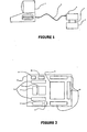
- the general arrangement within which the PLDPC as used is shown in Fig. 1.
- Software is provided which runs on the monitoring computer (MC) 1.
- the monitoring computer (MC) has a communications link 2 connecting it to the PLDPC 3.
- the monitoring computer (MC) talks to the PLDPC through the communications circuit (CC).
- the PLDPC itself has connectors 5 on its printed circuit board into which the communications circuit (CC) plugs.
- the PLDPC can function as a controller for peripheral circuits without the communications circuit (CC) and monitoring computer (MC), which are used for entering, editing, compiling, downloading, monitoring, testing and controlling user program circuits (UPCs).
- UPCs user program circuits
- the preferred embodiment of the PLDPC is as a core module shown in component block form in Fig. 2 and consists of a number of major components - the programmable logic device (PLD) 6, a fixed support circuit (FSC) 7, a flash memory (FM) 8, a phase locked loop (PLL) 9, a crystal oscillator 10, a voltage monitor and reset generator (VMRG) 11, and a power supply unit 12 consisting of voltage regulators, filtering and decoupling capacitors, all mounted on a printed circuit board 13 with various other minor components.
- Connectors 14 connect the PLDPC to the communications circuits (CC) and connectors 15 provide the PLDPC with I/O connections. Most of these items are not novel in themselves, but are listed to simplify understanding of the embodiment description.
- the novelty of this invention resides in the circuits loaded into the programmable logic device (PLD) and resident in the fixed support circuit (FSC), and the way all are used to implement PLDPC functionality as described in this specification.
- PLD programmable logic device
- FSC fixed support circuit
- the flash memory stores the user program circuit (UPC) and user program framework (UPF) configuration bit pattern (CBP) needed to configure the programmable logic device (PLD) to implement the user program circuit (UPC).
- the bit pattern is stored in the flash memory (FM) so that the CPLD can automatically configure the programmable logic device (PLD) when power comes on in the absence of the communications circuits (CC) and communications to the monitoring computer (MC), or if such a requirement is indicated by, for instance, a jumper on the printed circuit board.
- the PLDPC Core Module can be left to run independently without the monitoring computer (MC), communications link and communications circuits (CC). So that the system can restart independently after loss of power, the flash memory (FM) can also store necessary setup data required to initialize the system on power-up, including the value of the clock frequency chosen for the programmable logic device (PLD) and optionally all necessary system state data saved when the system last lost power.
- MC monitoring computer
- CC communications link and communications circuits
- the fixed support circuit (FSC) as used in the preferred embodiment is preconfigured in a CPLD, a fixed configuration (i.e. flash ROM based) logic device running at a constant clock frequency. It functions to configure the programmable logic device (PLD) and works with the communications circuits (CC) to read and write the flash memory (FM).
- the fixed support circuit (FSC) also contains circuits that operate with the phase locked loop (PLL) and determine the frequency of the clock supplied to the programmable logic device (PLD). It supplies and conditions the programmable logic device (PLD) reset signal.
- the fixed support circuit can optionally configure the programmable logic device (PLD) at power-up and establish necessary system values such as operating frequency, run or pause state, output enabling state, and restore system state data as per the last power-off, and so on.
- PLD programmable logic device
- the fixed support circuit could optionally be provided as fixed circuitry built into the programmable logic device (PLD) by the programmable logic device manufacturer with at least the benefit of reducing the chip count required to implement the PLDPC.
- PLD programmable logic device
- UPC user program circuit
- the software run on the monitoring computer may be arranged to automatically combine special circuitry, termed the user program framework (UPF) with the user program circuit (UPC).
- the user program framework can be provided as fixed circuitry built into the programmable logic device (PLD) by the programmable logic device manufacturer.
- the software includes a user program circuit (UPC) component library, and these components include necessary functionality to allow for the monitoring functions.
- the programmable logic device is a FPGA.
- phase locked loop is configured in a standard manner. It may be implemented using a Texas Instruments TLC2933 Phase Locked Loop integrated circuit, or similar device, together with dividers implemented in the fixed support circuit (FSC), in such a way as to generate selectable frequencies in response to values written into registers controlling the dividers.
- FSC fixed support circuit
- the TLC2933 can conveniently generate a selected frequency in the range 50 to 100MHz.
- a frequency may be selected at any 2MHz interval from 50 to 100MHz, and division of the selected frequency by an integer power of two can generate frequencies in the ranges of 25 to 50MHz, 12.5 to 25MHz, etc.
- the crystal oscillator, voltage monitor and reset generator (VMRG), and power supply unit are all standard components performing routine tasks.
- the monitoring computer is used to enter the user program circuit (UPC) via the schematic entry system of the software using a user program circuit (UPC) component library of functions implemented as described in GB 2371633, and using flip-flops that can be combined into a shift chain as also described.
- the software translates the schematic into a Hardware Description Language form, links each monitorable flip-flop (MFF) into the shift chain, adds the user program framework (UPF) and generates a configuration bit pattern (CBP) from it using standard programmable logic device (PLD) logic synthesis and fitting techniques.
- the result is a circuit which can be monitored, the flip-flops in the user program circuit (UPC) appear in a shift chain, and the functionality of each monitorable flip-flop (MFF) in the user program circuit (UPC) is known to the software.
- the shift chain is under the control of a state machine called the User Program Manager in the user program framework (UPF)
- the purpose of the user program manager is to switch the system between Logic Processing and Data Access modes of operation and to provide control as required to -
- the user program manager (UPM) described does not sequentially firstly latch input signals, then process the user program circuit (UPC), then provide data access, then latch output values. Rather, it latches input signals, processes the user program circuit (UPC), and latches output values each and every clock pulse that the user program circuit (UPC) clocking is enabled (See the discussion of the UPCEnable signal), and provides an alternative mode of operation to service monitor requests.
- Control and handshaking signals accessible to the monitoring computer (MC) enable the monitoring computer (MC) to request and control the necessary data access.
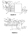
- the user program manager (UPM) is described with the aid of Figs. 3, 4, and 5.
- Fig. 3 shows the essential features of the user program framework (UPF), how the monitoring computer (MC) interacts with the user program manager (UPM) at the user program manager (UPM) interface, and how the user program manager (UPM) outputs signals for controlling the user program circuit (UPC).
- the circuit consists of two D flip-flops 16 and 17 with clock enables, the user program manager (UPM) state machine 18 as detailed in Fig.4.
- the preset and clear inputs on the flip-flops are of the synchronous type, as is the general case throughout the user program circuit (UPC).
- Fig. 4 is a listing of the user program manager (UPM) state machine code in the VHDL hardware description language.
- the listing can be compiled with Xilinx Ine's XST software and is suitable for behavioural simulation with Mentor Graphics' ModelSimTM simulator for the purpose of understanding the waveforms required to control the PLDPC.
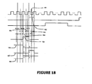
- Fig. 5 shows waveforms from a minimal propagation delay behavioural simulation of the listing in Fig. 4.
- the sequence now described demonstrates in particular how the monitoring computer (MC) can cause the user program manager (UPM) to enter pause mode, to single step, to enter continuous run mode, and to respond to a breakpoint in the form of the Break signal, and how it generates correctly timed enable signals for the user program circuit (UPC), the preload buffers and the late display buffer. Operation controlling multiple-stepping of the user program circuit (UPC), as opposed to single-stepping or continuous run, is not described because persons skilled in the art will easily see how to modify the user program manager (UPM) and add a counter loadable from the monitoring computer (MC), enabled to count and be interrogated by the user program manager (UPM) to enable the user program circuit (UPC) for a certain number of clock pulses.
- the PLDPC user program circuit is normally implemented with a single clock timing the storage of new states in all flip-flops in the user program circuit (UPC), although slower speed subsidiary clocks can be implemented if required.
- the clock signal is not gated, and therefore the clock signal is not made available to the user. This is enforced by the design of the user program circuit (UPC) component library provided. All of the monitorable flip-flops (MFFs) in the user program circuit (UPC) have their clock pins driven in parallel with the same clock signal via a low skew clock distribution system and operate on the same active clock transition (ACT).
- ACT active clock transition
- Clock enable inputs allow the user, when appropriate, to determine whether any particular flip-flop will be clocked by any particular active clock transition (ACT).
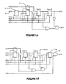
- Fig. 6 shows the type of monitorable flip-flop (MFF) that may be used in the user program circuit (UPC) component library items, but is not directly available to the user.
- the monitorable flip-flop (MFF) is essentially the same as that shown in Figure 10 of GB 2371633 which is reproduced herein as Fig. 7. The differences are:
- Input signals may be optionally asynchronous or synchronous.
- Traditional programmable controllers predominantly use asynchronous input signals.
- Asynchronous signals represent a problem in terms of being able to guarantee correct setup and hold times for following flip-flops, and require a protection circuit to ensure correct operation.
- Fig. 9 illustrates the principles of such a protection circuit.
- the signal can be sampled by a flip-flop 67 on the active clock transition (ACT) of clock 66 and allowed to settle for the remainder of the active transition interval (ATI) prior to sampling by following flip-flop 68 and ultimate delivery of the guaranteed signal 69 to following user program circuit (UPC) circuits, thereby allowing flip-flop 67 a defined period for settling to protect against metastability.
- ACT active clock transition
- UPC user program circuit
- the clock 66 for the protection circuit can be run at a slower rate synchronized to the main user program circuit (UPC) clock, if that is desirable and necessary to allow sufficient settling time to overcome metastability.
- UPC main user program circuit
- Flip-flop 68 can be omitted if the output signal from flip-flop 67 can be delivered exclusively to the inputs of other following flip-flops without any significant propagation delay, thereby preserving the settling time available to the output of flip-flop 67.
- the method provides for ease of use of input signals by the avoidance of setup and hold time problems although it introduces some delays. It is made available in the present invention by the use of special input terminal circuits and symbols from the user program circuit (UPC) component library.
- UPC user program circuit
- the peripheral circuits can also be arranged to present the necessary input signals in a synchronous manner with setup and hold times guaranteed to provide correct operation and referenced to a suitable clock edge or strobe.
- the signals may be distributed and used in the user program circuit (UPC) without the need for metastability hardening circuits, but the peripheral circuit timing requirements and design may be less convenient.
- UPC user program circuit
- asynchronous microprocessor data can be input to the system by latching the data with the trailing edge of the microprocessor write strobe, and then hardening each latched data bit using the circuit of Fig. 9.
- the latching is provided in our preferred embodiment by a latched output terminal circuit and symbol to be described later.
- Use of latching is mandatory if the output signals are derived from user program circuit (UPC) monitorable flip-flops (MFFs) because monitorable flip-flops (MFFs) may have their state values disturbed during the data access interval (DAI). Allowing logic to settle and latching the output state from the settled logic also provides glitch free outputs.
- UPC user program circuit
- MFFs monitorable flip-flops
- DAI data access interval Allowing logic to settle and latching the output state from the settled logic also provides glitch free outputs.
- the option of leaving outputs unlatched may be desirable for purely combinational logic pathways from input terminals, through the user program circuit (UPC), to output terminals, even though such applications may be in the minority.
- UPC user program circuit
- clock signal input 77 There is also a clock signal input 77 shown. The clock is distributed to each flip-flop to synchronize circuit operation.
- Each combinational logic block for example 72 consists of logic as required to provide the desired functionality.
- Circuit operation of a synchronous circuit of the type described consists of two steps repeating cyclically in time with the clock:
- an interface circuit can be combined together with the indirectly accessible device (IAD) to make a user program circuit (UPC) component library item that is directly usable in the user program circuit (UPC) and able to be accessed by the monitoring computer (MC).
- IAD indirectly accessible device
- UPC user program circuit
- the interface circuit for a RAM 82 is shown in Fig. 11, including:
- the circuits can be designed such that each shift of the shift chain increments the counter which is initially set to zero.
- the number in the counter suitably adjusted to allow for the data width, can be used as the memory address for accessing the RAM.
- the counter is arranged to roll over to zero when it is incremented past the value equivalent to the number of bits in the RAM. Because the shift chain is a circular shift register, as data is shifted out of the RAM interface downstream towards the monitoring computer (MC), other data is shifted into the interface from upstream. It is arranged that as each word, of whatever data width that may apply, is read out of the RAM to be shifted downstream, the word is replaced in the RAM by a word from upstream.
- the complete RAM contents, together with the other data in the shift chain, can be read and if necessary modified in one shift chain rotation.
- the RAM appears to the monitoring computer (MC) as a shift register in the shift chain of length equivalent to the number of bits in the RAM plus any additional bits used for temporary storage, etc.
- Communications between the user program framework (UPF) and the monitoring computer (MC) can use any appropriate and convenient technique, such as parallel I/O ports, an address and data bus arrangement, a serial link, and such like.
- user program circuit (UPC) monitorable flip-flops MFFs
- IAD indirectly accessible device-based
- UPC component library items are arranged to be part of the shift chain so that their state is accessible to the monitoring computer (MC) for display or modification purposes.
- User program framework (UPF) flip-flops do not normally appear in the shift chain.
- Combinational logic while it is visible on the user schematics, has no stored state data included in the shift chain.
- the user is able to display the state of any node within a combinational logic network by placing a special level display component on the schematic from the user program circuit (UPC) component library and connecting it to the node of interest.
- the level display component contains a monitorable flip-flop (MFF) that is automatically located in the shift chain by the software.
- the state may typically be displayed on a user program circuit (UPC) diagram as a '1' or '0' or as a graphic of a lamp that is on or off as at 96 on Fig. 12.
- the circuit for the level display is shown in Fig. 8, and is simply an monitorable flip-flop (MFF) as shown in Fig. 6 suitably connected.
- MFF monitorable flip-flop
- the monitorable flip-flop (MFF) is shown as a symbol 56 representing the circuit in Fig. 6.
- the signal assignments to the I/O connections in Fig. 8 are:
- the state of the monitorable flip-flop can be arranged to reflect the level on the node prior to the last user program circuit (UPC) enabled active clock transition (ACT) prior to the shift chain being read, or to reflect the state after the last user program circuit (UPC) enabled active clock transition (ACT) depending on the signal selected to drive CE pin 60.
- Pin CE is driven by the UPCEnable signal 33 for the former, and the PostRunClockEnable signal for the latter.
- a forcing buffer is provided, as a user program circuit (UPC) component library item, that allows the user to force user program circuit (UPC) signal levels to ⁇ 1' or '0' or leave them unforced.
- UPC user program circuit
- a graphic of a three position toggle switch 106 on the schematic symbol allows the user to choose "Force to 1", “Force to 0" or "transmit signal unchanged” using the monitoring computer (MC) and a mouse.
- An example of a user user program circuit (UPC) schematic is shown in Fig. 12, and shows such forcing buffers at 92 and 93.
- the user breaks the signal line at the point the forcing is to be applied and inserts the component in the signal line.
- the connection from the signal source goes to the forcing buffer input, and the connections to the signal loads are connected to the buffer output.
- Fig. 13 shows the circuit of the forcing buffer with an monitorable flip-flop (MFF) 109 arranged to provide an input level display and also a one clock delay.
- MFF monitorable flip-flop
- the forcing buffer is implemented using D flip-flops 110 and 111 inserted in the shift chain to store the forcing information, and combinational logic 112, 113 and 114 to derive the buffer output as required.
- Flip-flops 110 and 111 do not need to be monitorable flip-flops (MFFs) as they have no user customizable connections and are only accessible to the user via the monitoring computer (MC) and the shift chain.
- the circuit may also optionally provide an input and/or output display function in the manner of the level display component discussed previously.
- Flip-flop 110 when set indicates the output should be forced on, and flip-flop 111 indicates force off.
- the monitoring computer (MC) does not set both flip-flops 110 and 111 at the same time.
- the combined input level display and one clock delay may be omitted by:
- Input terminal symbols are used as the means whereby the user 'connects' the user program circuit (UPC) input points to external input signals via the physical terminals on the PLDPC using the monitoring computer (MC) and the software provided.
- the symbols used on the user program circuit (UPC) diagram may appear graphically as no more than simple terminals 97, 98, but assuming the signals connected are asynchronous and the terminals provide the preferred metastability protection, then they will at least contain hidden flip-flops. They may also contain display and forcing functionality as previously discussed.
- Fig. 14 shows an input terminal circuit providing forcing, input level display and metastability protection. Inspection will show that the circuit is identical to that of Fig. 13 with the addition of a D flip-flop 125 to the input signal circuit 126.
- the D flip-flop operates with the monitorable flip-flop (MFF) 127 as described for Fig. 9 to provide the metastability protection.
- MFF monitorable flip-flop
- Output terminal symbols 107 are used as the means whereby the user 'connects' the user program circuit (UPC) to external output signals via the physical terminals on the PLDPC using the monitoring computer (MC) and the software provided.
- the symbols provide output registers and will at least contain flip-flops. They may also contain display and forcing circuits as previously discussed.
- Output terminals may also be provided with the circuitry necessary to disable the outputs on demand, either from the user program circuit (UPC) or the monitoring computer (MC). Disabling may consist of either tri-stating the output, or switching it to whatever is considered the fail-safe level.
- UPS user program circuit
- MC monitoring computer
- Fig. 15 shows an output terminal circuit providing forcing, an monitorable flip-flop (MFF) providing a one cycle delay and data display, a final D flip-flop 128 to latch the output signal to hold it at a constant level during data access intervals (DAIs) and a gate 129 to disable the output when required. Inspection will show that the circuit is identical to the circuit of Fig. 13 with the addition of the final D flip-flop 128 and the disabling gate 129.
- MFF monitorable flip-flop
- DAIs data access intervals
- Level Display, Forcing Buffer, Input Terminal and Output Terminal circuits can be rearranged to provide various combinations of the features described as may be desired.
- Bidirectional terminals are provided by a combination of the input and output terminal methods with a tri-state capability.
- the user program circuit (UPC) component library function blocks will contain state values related to their function.
- a counter or a timer is probably the simplest example of this, with the state values being the number counted so far or the time left to run.
- the monitoring computer (MC) typically extracts these state values from the circuit state data and displays them as shown on the graphic of function block 95.
- the values displayed are not limited to numerical values, and may be displayed in a character based or symbolic form, or purely graphically as switches accessible to the user to change optional settings.
- functions such as state machines can also have their active states displayed by highlighting or colour changes.
- the monitoring computer (MC) also enables the user to modify values by double clicking them on the symbol and entering rew value into a dialog box that appears.
- the monitoring computer (MC) ensures that the new value, provided it is valid, is placed into the appropriate flip-flops in the user program circuit (UPC) via the shift chain.
- the user may, via the monitoring computer (MC), pause or single step the program, or run it continuously.
- Pausing the program is a matter of turning off the user program circuit (UPC) logic processing interval (LPI) clock enable.
- Single stepping is a matter of enabling the user program circuit (UPC) logic processing interval (LPI) clock enables for a single logic processing interval (LPI) clock cycle. All of this is done by the user program manager (UPM) in the user program framework (UPF), and has been described in conjunction with Figs. 3 and 4.
- the monitoring computer can single step the user program circuit (UPC), it can sequentially:
- This waveform display method has automatic access to all state data without a need to make any connections other than the normal monitoring computer (MC) connection.
- MC normal monitoring computer
- Breakpoints provide a way of trapping the occurrence of error or other conditions on which it is desirable to freeze the circuit and examine the circuit state.
- the user program circuit (UPC) component library provides breakpoint symbols. These allow a node or nodes in the user program circuit (UPC) to be connected by the user to the breakpoint input of the user program manager (UPM) such that when the node goes to ⁇ 1' or '0', as chosen by the user, the user program manager (UPM) senses the level change and causes the user program circuit (UPC) to halt by disabling the Logic Processing clock.
- the monitoring computer (MC) can access data to allow it to determine that a breakpoint has occurred and announce that to the user. This has been described in conjunction with Figs. 3 and 4.
- the user can either place suitable expression evaluating logic in the user program circuit (UPC) to generate the required breakpoint signal from the signals available, or the monitoring computer (MC) software can handle the necessary generation of the expression code and connections required.
- UPC user program circuit
- MC monitoring computer
- An alternative technique may be used to display waveforms, which removes much of the limitation due to the time taken to gather data.
- the alternative technique runs the user program circuit (UPC) in continuous run mode, maintaining control of it by automatically setting breakpoints prior to running it, and regaining control when a breakpoint is triggered.
- the monitoring computer (MC) can be sure that any signal causing a breakpoint trigger has only just changed to the specified trigger level in the clock cycle at which the trigger occurs, and has not been at that trigger level at any other time between when the monitoring computer (MC) started the continuous run and the trigger point.
- the monitoring computer can set the breakpoint again, but this time for the other level. That is, if it has just triggered by going to '1', then it will be set to trigger next when it goes to '0'. Repeating the steps of:
- the process can be implemented for more than one signal by:
- the user program circuit runs at full speed until a breakpoint occurs, and that the system can accumulate waveform data on as many signals as it is possible to set breakpoints on at any one time.
- the additional time added to the measurement process is broadly proportional to the number of clock cycles in which breakpoints trigger, that is in which signal transitions occur. Broadly, for waveform sets in which all signals are slow, that is in which transitions occur infrequently, waveform data may be accumulated at a speed approaching that of full continuous circuit operation.
- Any group of signals designated by the user as defining an integer or other multi-bit type may be displayed in a way suitable to that type, for example either as a numerical value, alphabetical value, or as an analogue value as displayed on an oscilloscope.
- Values other than the signals on which breakpoints are set, may also be recorded and displayed, although with the system so far described, only at the points in time at which breakpoints trigger. To do so, the monitoring computer simply logs the relevant shift chain data existing at each trigger point. The monitoring computer can then display these values, with or without also displaying the triggers.
- the monitoring computer (MC) may also be programmed to
- values representing slow analogue data can be sampled at fixed intervals, or complex circuit state values can be recorded at irregular intervals characterized by the occurrence of some defined combination of trigger signals, or sequence of combinations.
- the system as described allows the monitoring computer to be programmed to implement any advantageous combination of these possibilities.
- the run timer itself may advantageously be connected to the breakpoint system so that it triggers a break when its counter overflows and rolls over to zero.
- the monitoring computer becomes aware of the overflow and can keep track of the total number of cycles counted by the run timer, to a much larger value than the capacity of the run timer itself, thus enabling the circuit resources invested in the run timer to be minimized without significant disadvantage and with minimal slowing of circuit operation.
- monitoring computer using the techniques described, may be programmed, optionally while providing circuit stimuli via the shift chain as necessary, to:
- the run timer is either included in the shift chain, or otherwise made available to the monitoring computer, as most convenient so that its count value may be read and written.
- breakpoint circuitry suitable as a basis for a Long Timescale Waveform Display, although this circuitry may also be used advantageously for normal breakpoint implementations for debugging.
- the functionality provided includes -
- the user circuit enable (UCE) signal must be generated as shown in Fig. 3, where it is shown as 33 and going to the connector labeled UPCEnable.
- the method shown ensures that when the Break Signal 27 goes true during the breakpoint trigger pulse, the user program circuit (UPC) is immediately disabled by the AND gate that combines signals 19 and 27 to produce signal 33.
- the AND gate has an inverted input to which signal 27 is connected.
- signal 27 goes to '1' signal 33 immediately goes to ⁇ 0', hence preserving the user program circuit state that generated the breakpoint trigger.
- the user program circuit would operate for one more clock cycle, which is the time it takes the UPM state machine 18 to sense the break trigger pulse and turn off signal 19. The additional clock cycle operation would destroy the circuit state causing the break, making it unavailable for examination.
- the breakpoint circuit and system consists of a circuit block with an output that delivers a breakpoint trigger pulse, lasting a single user program circuit clock cycle, to the Break input 27 shown in Fig.3 whenever a breakpoint is triggered.
- the block has a convenient number of inputs for breakpoint trigger signals. These inputs are connected to signals in the user program circuit (UPC) by the user prior to the generation of the user program circuit (UPC) bit pattern to be downloaded into the PLD. These connections define the potential breakpoint trigger signals that may be enabled or disabled after the user program circuit (UPC) is downloaded and running.
- the block also has connections as convenient to enable the monitoring computer (MC) to use the functionality provided. These connections may for example be standard shift chain connections as previously described, and as shown for a single channel in Fig. 21.
- Each breakpoint channel as shown in Fig. 21 broadly consists of:
- the D flip-flop 172 is connected to one input of a 2 input XNOR gate 178 with the channel breakpoint trigger signal 175 connected to the other. Setting the flip-flop to ⁇ 0' or to '1' causes the XNOR gate to pass the breakpoint trigger signal either inverted or non-inverted respectively.
- the transition sensing circuit is arranged to generate a breakpoint trigger pulse 176 when the signal on the output of the XNOR gate goes from '0' to '1', so writing to the D flip-flop 172 allows the monitoring computer (MC) to control which transition of the channel breakpoint trigger signal 175 will generate the pulse.
- the signal from the XNOR gate 178 is passed to the D input of the monitorable flip-flop 177 via a two input AND gate 179 controlled by a signal 180 that gates it through only during the user circuit enable (UCE) time intervals.
- Signal 180 is the same signal shown as signal 19 in Fig. 3, and is not qualified by Break 27 as is signal 33, because the circuit is required to operate during the additional clock cycle that the AND gate generating signal 33 is designed to suppress when a break condition is generated.
- Flip-flop 177 is also clock enabled by signal 180.
- Flip-flop 174 is also clock enabled by signal 180 when the channel enable flip-flop 173 is set to '1', enable.
- signals 19 and 33 are identical.
- the user program circuit uses signal 33 as its user circuit enable (UCE) signal, which is its logic processing interval (LPI) clock enable signal.
- UAE user circuit enable
- LPI logic processing interval
- the breakpoint channel circuits which interface between the user program circuit (UPC) and the remainder of the system circuits such as the user program manager (UPM) state machine, use signal 19 to enable their operation during a logic processing interval (LPI).
- LPI logic processing interval
- MFFs monitorable flip-flops
- UPC monitorable flip-flops
- the Q output of flip-flop 177 When enabled during logic processing intervals (LPIs), the Q output of flip-flop 177 is the same as its D input except it is delayed by one user circuit enabled clock cycle. Feeding the signal on the D input 181 and the inverted signal from the Q output 182 to an AND gate 183 results in the AND gate outputting a breakpoint trigger pulse on signal 176 lasting one clock cycle each time the D input goes to '1' from '0'. Further, feeding the level from the D flip-flop 173 to a third input on the AND gate 183 allows the monitoring computer to enable or disable the generation of the pulse, thereby enabling and disabling the channel.
- LPIs logic processing intervals
- the final flip-flop 174 is arranged with two two-input multiplexers 184 and 185 so that it may either sample the breakpoint trigger signal 175 coming into the channel, or sample the breakpoint trigger pulse 176 generated by the three input AND gate 183, and these values can then be read by the monitoring computer (MC) via the shift chain.
- Signal selection is controlled by the D flip-flop 173 as a secondary function in addition to its primary function of disabling or enabling the channel. This is convenient because the monitoring computer needs to read the level of the breakpoint trigger signal coming into the channel when this flip-flop is disabled before the start of a run and read the breakpoint trigger pulse 176 from the three input AND gate 183 when the channel is enabled during a run.
- Multiplexer 184 feeds the D input 186 of the monitorable flip-flop 174 with the breakpoint trigger pulse signal 176 when the channel is enabled, and when the channel is disabled with the breakpoint trigger signal 175.
- Multiplexer 185 feeds the clock enable input 187 of the monitorable flip-flop 174 with non-truncated user circuit enabling signal 180 when the channel is enabled, and when the channel is disabled with a specially timed sampling signal 188 called the tap clock enable (TCE).
- TCE tap clock enable
- the tap clock enable signal (TCE) 188 is generated by a simple modification of the User Program Manager (UPM) state machine of Fig 4 The signal is arranged to occur for one clock cycle only immediately after each time the UPM user circuit enable signal 19 goes to '0' from '1'. Signal 19 is driven by the port UPCEnable defined in the VHDL code of Fig. 4.
- the flip-flop 174 By enabling the flip-flop 174 using the tap clock enable signal 188, the flip-flop can be made to sample the state of the breakpoint trigger signal level 176 at the correct time, after it has settled following the completion of the logic processing interval (LPI) and prior to its value being read by the monitoring computer (MC) during the next data access interval (DAI).
- Fig. 21 does not show connections for initializing the flip-flops after the PLD configuration bit pattern is downloaded. It may be convenient to connect these to initialize to a circuit state of:
- transition polarity selecting flip-flop 172 may have its state automatically reversed each time its associated breakpoint trigger signal 175 generates a breakpoint trigger pulse 176, as is required for continued trigger monitoring.
- the user has the following facilities to help debug and commission a user program circuit (UPC). They may:
- the user program circuit (UPC) is implemented using logic as described in the section Synchronous logic above.
- Fig. 16 shows waveforms associated with normal monitored semi-continuous run operation.
- the clock 130 runs continuously, and the associated active clock transitions (ACTs), for example 144, are the positive going edges.
- ACTs active clock transitions
- the user program circuit is enabled for active clock transitions (ACTs) during the logic processing interval (LPI) which is when the UPCEnable signal 131 is high (true).
- the ShiftChainEnable signal 132 goes high (true) during the data access interval (DAI).
- Logic processing intervals (LPIs) and data access intervals (DAIs) alternate repeatedly. Between each logic processing interval (LPI) and data access interval (DAI) is a period of time, which is much longer than the time normally available for the logic to settle, when neither UPCEnable nor ShiftChainEnable is high.
- This period corresponds to the time taken for the user program manager (UPM) state machine to change its active state from the state controlling the logic processing interval (LPI) to the state(s) controlling the data access interval (DAI) and vice-versa.
- the dotted lines in Fig. 16 indicate continuance for an undefined number of clock cycles wherein the clock continues with the same waveform and at the same frequency, and the other signals continue at the indicated levels.
- LPI logic processing interval
- ATI active transition interval
- each run mode active transition interval (ATI), for example, ATI n 136, and the run mode active transition interval (ATI) prior to it, ATI n-1 137 are characterized by the particular pattern of '1's and '0's, denoted as P n and P n-1 , representing the settled output levels for the user program circuit (UPC) flip-flops for each active transition interval (ATI) respectively, and determined by the operation of the circuit and the circuit stimuli.
- P n and P n-1 representing the settled output levels for the user program circuit (UPC) flip-flops for each active transition interval (ATI) respectively, and determined by the operation of the circuit and the circuit stimuli.
- An example of such a pattern is shown in Fig. 16, but for three flip-flop output signals only for brevity's sake.
- the pattern P n for output signals 138, 139 and 140 is 0, 1, 1 respectively, and in time interval 135, the pattern P n-1 is 0, 0, 1.
- LPI logic processing interval
- ATI active transition interval
- the user program circuit (UPC) flip-flop output levels generated by the last active clock transition (ACT) in any one logic processing interval (LPI), for example 143, are those that, once they have propagated through any intervening combinational logic to the following flip-flops, will be sampled by the first active clock transition (ACT) in the next logic processing interval (LPI), for example 147.
- the monitorable flip-flops (MFFs) in the user program circuit (UPC) as so far described, will have their states disturbed during the data access interval (DAI), for example 146, due to the shift chain operation, but will all be restored and loaded with the correct state data when data accessing is complete some clock cycles before the next logic processing interval (LPI) active clock transition (ACT).
- DAI data access interval
- LPI logic processing interval
- ACT logic processing interval
- the user program circuit (UPC) state data will not change during the interval 141 between the data access interval (DAI) 146 and logic processing interval (LPI) 142 because neither the UPCEnable nor the ShiftChainEnable levels are true and all the monitorable flip-flops (MFFs) are disabled.
- Combinational logic output signals resulting from monitorable flip-flop (MFF) output levels generated by the last active clock transition (ACT) in an logic processing interval (LPI) therefore have a significantly longer time to settle and stabilize, at least several clock cycles, before being sampled than if the generating active clock transition (ACT) had not been the last in the logic processing interval (LPI), when there is only a single Logic Settling Interval.
- MFF monitorable flip-flop
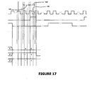
- Fig. 17 shows waveforms applicable to single stepping.
- Single step mode is of course an extreme case where every logic processing interval (LPI) active clock transition (ACT) is both the first and the last in the logic processing interval (LPI), because each logic processing interval (LPI) is only one active transition interval (ATI) long.
- LPI logic processing interval
- ACT active clock transition
- ATI active transition interval
- active transition interval (ATI) 137 the pattern P n-1 is the resultant of the sampling by the logic processing interval (LPI) active clock transition (ACT) at the start of 137, however, in active transition interval (ATI) 149 we see the same pattern as 148, the result of the data restoration at the end of the data access interval (DAI), rather than sampling during the previous logic processing interval (LPI) active clock transition (ACT).
- the previous logic processing interval (LPI) active clock transition (ACT) is of course some significant time before, and prior to the data access interval (DAI).
- the first criteria is complied with because we have control of the clock frequency.
- the second is complied with because the principles of operation of the invention provide compliance, even if settling times are not required to be identical in both run and single step mode.
- the additional means are required to meet the third criteria.
- the logic patterns during intervals 145 and 153 are maintained the same by the operation of the circuits so far described, by virtue of the fact that after a rotation of the shift chain, the original user program circuit (UPC) state data from the end of the last logic processing interval (LPI) is intentionally returned to its original position in the user program circuit (UPC) for the start of the next logic processing interval (LPI). That is, unless it has been modified by the monitoring computer (MC), which of course would be an intended and acceptable situation.
- UPC original user program circuit
- LPI last logic processing interval
- MC monitoring computer
- the logic patterns during intervals 135 and 154 represent a different case.
- the logic pattern in interval 135 represents the user program circuit (UPC) state data one logic processing interval (LPI) active clock transition (ACT) before that of interval 145. In continuous run mode these waveforms are generated naturally by the circuit operation.
- UPC user program circuit
- LPI logic processing interval
- ACT active clock transition
- the PreloadEnable signal 155 is provided by the user program manager (UPM) state machine to enable the correct values to be inserted by a multiplexer onto the inputs to the user program circuit (UPC) combinational logic.
- the values required for insertion are those that existed on the outputs of the corresponding user program circuit (UPC) monitorable flip-flops (MFFs) just prior to the last logic processing interval (LPI) active clock transition (ACT), and so if the user program circuit (UPC) monitorable flip-flop (MFF) outputs are sampled and stored every logic processing interval (LPI) active clock transition (ACT) the stored values will always automatically be the values required for insertion.
- Fig. 19 shows the circuit of Fig. 6 suitably modified to add the sampling, storage and multiplexing.
- the required flip-flop output pattern is applied to the combinational logic at the start of the logic settling interval in the active transition interval (ATI) immediately prior to the single step logic processing interval (LPI) active transition interval (ATI), and the logic settling conditions in continuous run and single-step modes are made sufficiently identical.
- ATI active transition interval
- LPI single step logic processing interval
- ATI single step logic processing interval
- circuits can be built into monitorable flip-flops (MFFs) to work with the PreloadEnable signal to control combinational logic settling conditions in single step mode.
- MFFs monitorable flip-flops
- Such circuits can also be provided in a form allowing the user to add them explicitly to user program circuit (UPC) schematics as appropriate symbols, and the monitoring computer (MC) can automatically make the necessary connections to standard signals such as PreloadEnable.
- UPC user program circuit
- MC monitoring computer
- one aspect of this invention is the provision of a self contained automated test method for determining the maximum allowable clock speed for correct operation.
- test method used results in a measure of the performance of the individual piece of hardware on which the test is performed and in the conditions under which it was performed, rather than, as in the case of simulation based design, a necessarily conservative estimate of the level of performance that can be expected from any hardware complying with the specifications applicable to the simulations. This is a significant difference which provides a useful choice particularly to users who need to implement one-off or small numbers of systems working at maximum performance.
- a safety margin should also always be allowed to provide for inherent variability of circuit elements, variability test run to test run, and over time. The safety margin should be determined based on experience with particular hardware systems due to its dependence on many factors, for example clock jitter.
- test method used consists of:
- the user defines sets of user program circuit (UPC) stimulus conditions that can be expected to lead to worst case settling times, in a similar way to how they would define the stimuli with which to simulate a circuit if using the simulation method of design implementation.
- the set of initial stimulus conditions are used for both the reference and subsequent test runs.
- the monitoring computer provides a special Record Test Run mode of operation, operating with the above mentioned extended logic settling times, whereby the user forces or sets necessary initial circuit conditions for each test.
- Preload Buffers to be described may also be used.
- the user can drive a signal from a level, the resultant of a logic expression or a clocked pattern by driving Forcing or Preload Buffer inputs from a suitable source.
- Forcing buffers allow sections of the circuit to be isolated for separate tests.
- Test vector stimuli may also be generated as convenient by user defined generators.
- the user When the initial conditions are set, the user single or multiple steps the user program circuit (UPC) and full sets of user program circuit (UPC) state data are recorded by the monitoring computer (MC) before and after each logic processing interval (LPI) active clock transition (ACT).
- the resultant stimuli and responses associated with each logic processing interval (LPI) active clock transition (ACT) can be observed with the waveform display during the recording process and then saved on the monitoring computer (MC) under a user-chosen name. Because the response produced by one logic processing interval (LPI) active clock transition (ACT) is also the stimulus for the next when multiple steps are taken, it is of course not necessary to record the redundant data.
- the monitoring computer has a set of initial states for the user program circuit (UPC), which if applied prior to a single logic processing interval (LPI) active clock transition (ACT) will each produce an associated known response providing that the user program circuit (UPC) operates error free.
- LPI logic processing interval
- ACT active clock transition
- Fig. 20 shows the internal circuit for the Preload Buffer, which is very simple and consists of just a two input multiplexer 167 properly connected.
- Preload Buffer signal 170 selects between signals 168 and 169, connecting the selected signal to output 171.
- Signal 170 is driven from signal PreloadEnable 34.
- PreloadEnable is true for one clock cycle before each time that UPCEnable goes true. When PreloadEnable is true it selects signal 168 otherwise signal 169 is selected.
- Fig. 12 shows how Forcing and Preload Buffers may be used in a user program circuit (UPC).
- Block 94 is a circuit block consisting of combinational logic only, and having inputs 99, 100 and 101. Block 94 has a single output of concern 102 driving another circuit block 95. If it is suspected that the maximum settling for a circuit under test is caused when signal 101, normally driven by Pin 98, goes from '1' to '0', the user can proceed as follows -
- the procedure described ensures that the signal only has one active transition interval (ATI) in which to settle, even though the UPCEnable signal only comes true for one clock cycle at a time, each time many clock cycles apart.
- ATI active transition interval
- a test automatically controlled by the monitoring computer (MC), consists of:
- MFF monitorable flip-flop
- Loading a full set of initial state data for each logic processing interval (LPI) clock cycle instead of starting the next test with the state data produced by the last, and doing so even if the cycle was recorded as part of a multi-cycle test, allows the system to check for correct operation during each cycle of the multi-cycle test, even if some previous cycles had exhibited incorrect behaviour.
- This method provides maximum information by allowing the system to report system performance cycle by cycle for all planned test cycles, and to report in terms of all the bits in all the components that failed in each cycle that exhibited incorrect behaviour.
- a minor limitation of the method occurs when two errors exist in consecutive logic processing interval (LPI) active transition intervals (ATIs). Whereas the correct state data pattern will be loaded from the monitoring computer (MC) for the single step logic processing interval (LPI) active transition interval (ATI), the data for the preload active transition interval (ATI) will be that which was stored in the logic processing interval (LPI) active transition interval (ATI) prior to the preload cycle, and this may have an adverse effect on the settling of the data for the single step logic processing interval (LPI) active transition interval (ATI).
- a computer is programmed to generate a description of the user program circuit and control circuits thus arranged.
- the description may be, for example, a hardware description language version of the combined circuits.
- This description may subsequently be compiled into a bit pattern for programming the PLD.
- the compiler may be integrated, so that the description is the bit pattern for programming the PLD.
- the computer may be programmed to generate a hardware description language version of the user program circuit, excluding the control circuit. That is, the computer may generate a circuit excluding features only required to support the monitoring computer monitoring functions and the various control circuits. This version of the user program circuit may be used for compiling or simulating equivalent circuits without the monitoring functions.
Landscapes
- Physics & Mathematics (AREA)
- Mathematical Physics (AREA)
- Engineering & Computer Science (AREA)
- Computing Systems (AREA)
- Automation & Control Theory (AREA)
- Computer Hardware Design (AREA)
- General Physics & Mathematics (AREA)
- General Engineering & Computer Science (AREA)
- Logic Circuits (AREA)
- Programmable Controllers (AREA)
- Ultra Sonic Daignosis Equipment (AREA)
- Holo Graphy (AREA)
- Pinball Game Machines (AREA)
Applications Claiming Priority (3)
| Application Number | Priority Date | Filing Date | Title |
|---|---|---|---|
| NZ53513004A NZ535130A (en) | 2004-09-03 | 2004-09-03 | Improvements in or relating to programmable logic controller and related electronic devices |
| NZ53575704 | 2004-10-04 | ||
| NZ53753604 | 2004-12-24 |
Publications (3)
| Publication Number | Publication Date |
|---|---|
| EP1632825A2 true EP1632825A2 (fr) | 2006-03-08 |
| EP1632825A3 EP1632825A3 (fr) | 2007-02-21 |
| EP1632825B1 EP1632825B1 (fr) | 2008-10-29 |
Family
ID=35478961
Family Applications (1)
| Application Number | Title | Priority Date | Filing Date |
|---|---|---|---|
| EP05255419A Expired - Lifetime EP1632825B1 (fr) | 2004-09-03 | 2005-09-05 | Ameliorations apportées ou relatives à des contrôleurs logiques programmables et dispositifs électroniques apparentés |
Country Status (4)
| Country | Link |
|---|---|
| US (2) | US20060079970A1 (fr) |
| EP (1) | EP1632825B1 (fr) |
| AT (1) | ATE412932T1 (fr) |
| DE (1) | DE602005010639D1 (fr) |
Cited By (1)
| Publication number | Priority date | Publication date | Assignee | Title |
|---|---|---|---|---|
| CN111400384A (zh) * | 2020-03-11 | 2020-07-10 | 广东溢达纺织有限公司 | 浆纱机监控系统、方法、计算机设备和存储介质 |
Families Citing this family (29)
| Publication number | Priority date | Publication date | Assignee | Title |
|---|---|---|---|---|
| KR101079592B1 (ko) * | 2006-11-03 | 2011-11-04 | 삼성전자주식회사 | 디스플레이장치 및 그 정보갱신방법 |
| US8352651B2 (en) * | 2007-06-12 | 2013-01-08 | Siemens Aktiengesellschaft | Devices, systems, and methods regarding programmable logic controller communications |
| US7646230B2 (en) * | 2007-09-21 | 2010-01-12 | Siemens Industry, Inc. | Devices, systems, and methods for reducing signals |
| US8305903B1 (en) * | 2008-03-31 | 2012-11-06 | C Speed, Llc | Data acquisition system for test and measurement signals |
| US8140832B2 (en) * | 2009-01-23 | 2012-03-20 | International Business Machines Corporation | Single step mode in a software pipeline within a highly threaded network on a chip microprocessor |
| WO2010121109A1 (fr) * | 2009-04-17 | 2010-10-21 | Siemens Aktiengesellschaft | Descriptions de séquence alternée pour produire des trajets d'exécution alternés dans un système d'automatisation |
| US7859245B2 (en) * | 2009-04-27 | 2010-12-28 | Ansaldo Sts Usa, Inc. | Apparatus, system and method for outputting a vital output for a processor |
| US9448964B2 (en) * | 2009-05-04 | 2016-09-20 | Cypress Semiconductor Corporation | Autonomous control in a programmable system |
| US8670859B2 (en) * | 2009-07-09 | 2014-03-11 | Siemens Industry, Inc. | Methods and apparatus for an improved motor control center |
| US20110302329A1 (en) * | 2010-06-03 | 2011-12-08 | Asad Azam | Embedded Programmable Module for Host Controller Configurability |
| JP5691752B2 (ja) * | 2011-04-01 | 2015-04-01 | セイコーエプソン株式会社 | データの書き換え方法、データ書き換え装置及び書き換えプログラム |
| CN103631316B (zh) * | 2012-08-21 | 2020-06-26 | 是德科技股份有限公司 | 用于输出复杂触发信号的多级触发系统 |
| US9064053B2 (en) * | 2012-12-05 | 2015-06-23 | The Mathworks, Inc. | Integrating diagnostic information with boolean constraints |
| US8912935B1 (en) * | 2013-05-09 | 2014-12-16 | Maxim Integrated Products, Inc. | Digital input for a programmable logic controller |
| US20150147731A1 (en) * | 2013-05-15 | 2015-05-28 | Julia Pavlovna Astafiev | Shifting visual attention between multiple video displays to train attention and memory |
| JP6176407B2 (ja) * | 2014-09-11 | 2017-08-09 | 三菱電機株式会社 | 入出力制御装置、入出力制御方法、及びプログラム |
| US9672135B2 (en) | 2015-11-03 | 2017-06-06 | Red Hat, Inc. | System, method and apparatus for debugging of reactive applications |
| US9703546B1 (en) * | 2015-12-21 | 2017-07-11 | Schneider Electric Software, Llc | Monitoring application states for deployment during runtime operations |
| CN106656121B (zh) * | 2016-11-30 | 2024-07-05 | 吉林大学 | 一种亚纳秒级数字延时脉冲发生装置及工作方法 |
| KR102353027B1 (ko) * | 2017-07-03 | 2022-01-20 | 삼성전자주식회사 | 스토리지 장치의 데이터 트레이닝 방법 |
| US10621067B1 (en) * | 2018-02-05 | 2020-04-14 | Xilinx, Inc. | Data unit breakpointing circuits and methods |
| EP3647801A1 (fr) * | 2018-10-30 | 2020-05-06 | dSPACE digital signal processing and control engineering GmbH | Procédé de vérification d'un programme fpga |
| US11044167B2 (en) * | 2019-03-06 | 2021-06-22 | The Toronto-Dominion Bank | Intraday resource management system |
| US11869070B2 (en) | 2019-03-06 | 2024-01-09 | The Toronto-Dominion Bank | Expected transfer monitoring and notification |
| CN110529199A (zh) * | 2019-07-26 | 2019-12-03 | 南京国电南自维美德自动化有限公司 | 一种支持控制逻辑重配置的汽轮机阀门控制方法、装置和系统 |
| CN110865559A (zh) * | 2019-10-09 | 2020-03-06 | 上海星沿工业智能科技有限公司 | 工装控制系统及方法、设备、存储介质 |
| CN112290913A (zh) * | 2020-11-05 | 2021-01-29 | 中山大学 | 一种大功率超宽带电磁脉冲强制同步方法 |
| CN114779883B (zh) * | 2022-05-17 | 2024-03-19 | 西安易朴通讯技术有限公司 | 系统时钟同步方法、装置、系统及存储介质 |
| CN114741022B (zh) * | 2022-05-18 | 2023-05-16 | 合肥召洋电子科技有限公司 | 一种双备份控制电路供电电路载体及配置方法 |
Family Cites Families (124)
| Publication number | Priority date | Publication date | Assignee | Title |
|---|---|---|---|---|
| NZ218742A (en) * | 1986-06-03 | 1990-09-26 | Fisher & Paykel | Programmed logic controller |
| US4303990A (en) | 1976-07-01 | 1981-12-01 | Gulf & Western Industries, Inc. | Programmable controller using microprocessor |
| US4117317A (en) * | 1976-08-09 | 1978-09-26 | Dynage, Incorporated | Programmable controller with hardwired backup connecting terminals and related control system using programmable controller and hardwired backup |
| US4275455A (en) * | 1977-07-11 | 1981-06-23 | Automation Systems, Inc. | Output interface card suitable for use with a programmable logic controller |
| US4845627A (en) * | 1987-10-01 | 1989-07-04 | Eaton Corporation | Remote programmable controller |
| GB2220280B (en) | 1988-07-04 | 1992-10-21 | Rolls Royce & Ass | A control system for industrial plant |
| US5166604A (en) | 1990-11-13 | 1992-11-24 | Altera Corporation | Methods and apparatus for facilitating scan testing of asynchronous logic circuitry |
| DE69327389T2 (de) * | 1992-10-29 | 2000-06-15 | Altera Corp., San Jose | Verfahren zum Prüfen von Entwürfen für programmierbare Logikschaltungen |
| US5498975A (en) * | 1992-11-19 | 1996-03-12 | Altera Corporation | Implementation of redundancy on a programmable logic device |
| US5617327A (en) | 1993-07-30 | 1997-04-01 | Xilinx, Inc. | Method for entering state flow diagrams using schematic editor programs |
| US5369314A (en) | 1994-02-22 | 1994-11-29 | Altera Corporation | Programmable logic device with redundant circuitry |
| US5590305A (en) | 1994-03-28 | 1996-12-31 | Altera Corporation | Programming circuits and techniques for programming logic |
| US5550843A (en) * | 1994-04-01 | 1996-08-27 | Xilinx, Inc. | Programmable scan chain testing structure and method |
| US5802540A (en) * | 1995-11-08 | 1998-09-01 | Altera Corporation | Programming and verification address generation for random access memory blocks in programmable logic array integrated circuit devices |
| US5617573A (en) * | 1994-05-23 | 1997-04-01 | Xilinx, Inc. | State splitting for level reduction |
| GB2297409B (en) | 1995-01-27 | 1998-08-19 | Altera Corp | Programmable logic devices |
| US5528169A (en) * | 1995-04-26 | 1996-06-18 | Xilinx, Inc. | Method and structure for providing a flip flop circuit with a configurable data input path |
| EP0823091A1 (fr) * | 1995-04-28 | 1998-02-11 | Xilinx, Inc. | Microprocesseur a registres repartis accessibles par logique programmable |
| US5761483A (en) * | 1995-08-18 | 1998-06-02 | Xilinx, Inc. | Optimizing and operating a time multiplexed programmable logic device |
| US5600263A (en) * | 1995-08-18 | 1997-02-04 | Xilinx, Inc. | Configuration modes for a time multiplexed programmable logic device |
| US5784313A (en) | 1995-08-18 | 1998-07-21 | Xilinx, Inc. | Programmable logic device including configuration data or user data memory slices |
| US5701441A (en) | 1995-08-18 | 1997-12-23 | Xilinx, Inc. | Computer-implemented method of optimizing a design in a time multiplexed programmable logic device |
| US5838954A (en) | 1995-08-18 | 1998-11-17 | Xilinx, Inc. | Computer-implemented method of optimizing a time multiplexed programmable logic device |
| US5583450A (en) | 1995-08-18 | 1996-12-10 | Xilinx, Inc. | Sequencer for a time multiplexed programmable logic device |
| US5629637A (en) * | 1995-08-18 | 1997-05-13 | Xilinx, Inc. | Method of time multiplexing a programmable logic device |
| US5745734A (en) * | 1995-09-29 | 1998-04-28 | International Business Machines Corporation | Method and system for programming a gate array using a compressed configuration bit stream |
| US5555214A (en) * | 1995-11-08 | 1996-09-10 | Altera Corporation | Apparatus for serial reading and writing of random access memory arrays |
| US5650734A (en) * | 1995-12-11 | 1997-07-22 | Altera Corporation | Programming programmable transistor devices using state machines |
| US5764079A (en) * | 1996-03-11 | 1998-06-09 | Altera Corporation | Sample and load scheme for observability of internal nodes in a PLD |
| US6020758A (en) * | 1996-03-11 | 2000-02-01 | Altera Corporation | Partially reconfigurable programmable logic device |
| US5875112A (en) * | 1996-03-20 | 1999-02-23 | Altera Corporation | Methods for implementing circuit designs in physical circuits |
| US5898628A (en) * | 1996-04-19 | 1999-04-27 | Altera Corporation | Data transfer circuit |
| US5870410A (en) * | 1996-04-29 | 1999-02-09 | Altera Corporation | Diagnostic interface system for programmable logic system development |
| US6195772B1 (en) * | 1996-06-21 | 2001-02-27 | Altera Corporaiton | Electronic circuit testing methods and apparatus |
| US6233205B1 (en) * | 1996-09-17 | 2001-05-15 | Xilinx, Inc. | Built-in self test method for measuring clock to out delays |
| US6178494B1 (en) * | 1996-09-23 | 2001-01-23 | Virtual Computer Corporation | Modular, hybrid processor and method for producing a modular, hybrid processor |
| US6110223A (en) | 1996-10-28 | 2000-08-29 | Altera Corporation | Graphic editor for block diagram level design of circuits |
| US5963565A (en) | 1996-10-31 | 1999-10-05 | Altera Corporation | Apparatus and method for external supervision of electronic test equipment operating parameters |
| US5844422A (en) | 1996-11-13 | 1998-12-01 | Xilinx, Inc. | State saving and restoration in reprogrammable FPGAs |
| US6134707A (en) * | 1996-11-14 | 2000-10-17 | Altera Corporation | Apparatus and method for in-system programming of integrated circuits containing programmable elements |
| US6490714B1 (en) | 1996-11-27 | 2002-12-03 | Altera Corporation | Apparatus and method for in-system programming of a field programmable logic device using device-specific characterization data |
| US6034536A (en) * | 1997-02-05 | 2000-03-07 | Altera Corporation | Redundancy circuitry for logic circuits |
| US6091258A (en) * | 1997-02-05 | 2000-07-18 | Altera Corporation | Redundancy circuitry for logic circuits |
| US6085317A (en) * | 1997-08-15 | 2000-07-04 | Altera Corporation | Reconfigurable computer architecture using programmable logic devices |
| EP0983549B1 (fr) * | 1997-05-23 | 2001-12-12 | Altera Corporation (a Delaware Corporation) | Circuits redondants pour dispositifs a logique programmable a circuits d'entree entrelaces |
| US6691267B1 (en) * | 1997-06-10 | 2004-02-10 | Altera Corporation | Technique to test an integrated circuit using fewer pins |
| US6539510B1 (en) * | 1997-08-12 | 2003-03-25 | Xilinx, Inc. | Interface board for receiving modular interface cards |
| US6608638B1 (en) * | 2000-02-07 | 2003-08-19 | National Instruments Corporation | System and method for configuring a programmable hardware instrument to perform measurement functions utilizing estimation of the hardware implentation and management of hardware resources |
| US6802053B1 (en) | 1997-08-18 | 2004-10-05 | National Instruments Corporation | Graphical programming system with distributed block diagram execution and front panel display |
| US6173438B1 (en) * | 1997-08-18 | 2001-01-09 | National Instruments Corporation | Embedded graphical programming system |
| US6784903B2 (en) * | 1997-08-18 | 2004-08-31 | National Instruments Corporation | System and method for configuring an instrument to perform measurement functions utilizing conversion of graphical programs into hardware implementations |
| US6311149B1 (en) | 1997-08-18 | 2001-10-30 | National Instruments Corporation | Reconfigurable test system |
| US6219628B1 (en) * | 1997-08-18 | 2001-04-17 | National Instruments Corporation | System and method for configuring an instrument to perform measurement functions utilizing conversion of graphical programs into hardware implementations |
| US6078736A (en) * | 1997-08-28 | 2000-06-20 | Xilinx, Inc. | Method of designing FPGAs for dynamically reconfigurable computing |
| US6202185B1 (en) * | 1997-10-15 | 2001-03-13 | Altera Corporation | Methods and apparatus for facilitating scan testing of circuitry |
| US6157210A (en) | 1997-10-16 | 2000-12-05 | Altera Corporation | Programmable logic device with circuitry for observing programmable logic circuit signals and for preloading programmable logic circuits |
| US6247147B1 (en) * | 1997-10-27 | 2001-06-12 | Altera Corporation | Enhanced embedded logic analyzer |
| US6286114B1 (en) | 1997-10-27 | 2001-09-04 | Altera Corporation | Enhanced embedded logic analyzer |
| US5986467A (en) | 1997-10-31 | 1999-11-16 | Xilinx, Inc. | Time-multiplexed programmable logic devices |
| US6526566B1 (en) * | 1997-11-14 | 2003-02-25 | National Instruments Corporation | Graphical programming system and method including nodes for programmatically accessing data sources and targets |
| EP1677195A3 (fr) * | 1997-11-18 | 2011-06-22 | Altera Corporation | Analyseur logique intégré amélioré |
| US6212650B1 (en) * | 1997-11-24 | 2001-04-03 | Xilinx, Inc. | Interactive dubug tool for programmable circuits |
| US5970005A (en) | 1998-04-27 | 1999-10-19 | Ict, Inc. | Testing structure and method for high density PLDs which have flexible logic built-in blocks |
| US6625795B1 (en) | 1998-06-29 | 2003-09-23 | Xilinx, Inc. | Method and apparatus for placement of input-output design objects into a programmable gate array |
| US6201404B1 (en) * | 1998-07-14 | 2001-03-13 | Altera Corporation | Programmable logic device with redundant circuitry |
| EP1138001B1 (fr) | 1998-11-20 | 2003-08-27 | Altera Corporation | Systeme informatique a logique programmable reconfigurable |
| US6167001A (en) | 1999-01-26 | 2000-12-26 | Xilinx, Inc. | Method and apparatus for measuring setup and hold times for element microelectronic device |
| US6107821A (en) * | 1999-02-08 | 2000-08-22 | Xilinx, Inc. | On-chip logic analysis and method for using the same |
| US6255848B1 (en) * | 1999-04-05 | 2001-07-03 | Xilinx, Inc. | Method and structure for reading, modifying and writing selected configuration memory cells of an FPGA |
| US6618686B2 (en) | 1999-05-14 | 2003-09-09 | Xilinx, Inc. | System and method for testing a circuit implemented on a programmable logic device |
| US6425077B1 (en) * | 1999-05-14 | 2002-07-23 | Xilinx, Inc. | System and method for reading data from a programmable logic device |
| US6292116B1 (en) | 1999-05-17 | 2001-09-18 | Altera Corporation | Techniques and circuitry for accurately sampling high frequency data signals input to an integrated circuit |
| US6239611B1 (en) * | 1999-06-10 | 2001-05-29 | Xilinx, Inc. | Circuit and method for testing whether a programmable logic device complies with a zero-hold-time requirement |
| US6246258B1 (en) * | 1999-06-21 | 2001-06-12 | Xilinx, Inc. | Realizing analog-to-digital converter on a digital programmable integrated circuit |
| US6452459B1 (en) | 1999-07-22 | 2002-09-17 | Xilinx, Inc. | Circuit for measuring signal delays of synchronous memory elements |
| US6507211B1 (en) * | 1999-07-29 | 2003-01-14 | Xilinx, Inc. | Programmable logic device capable of preserving user data during partial or complete reconfiguration |
| US6625787B1 (en) | 1999-08-13 | 2003-09-23 | Xilinx, Inc. | Method and apparatus for timing management in a converted design |
| US6463339B1 (en) | 1999-09-27 | 2002-10-08 | Rockwell Automation Technologies, Inc. | High reliability industrial controller using tandem independent programmable gate-arrays |
| US6629311B1 (en) | 1999-11-17 | 2003-09-30 | Altera Corporation | Apparatus and method for configuring a programmable logic device with a configuration controller operating as an interface to a configuration memory |
| US6748368B1 (en) * | 2000-01-05 | 2004-06-08 | Xilinx, Inc. | Proprietary core permission structure and method |
| US6584601B1 (en) * | 2000-02-07 | 2003-06-24 | National Instruments Corporation | System and method for converting graphical programs into hardware implementations which utilize probe insertion |
| US6487709B1 (en) | 2000-02-09 | 2002-11-26 | Xilinx, Inc. | Run-time routing for programmable logic devices |
| US6625797B1 (en) | 2000-02-10 | 2003-09-23 | Xilinx, Inc. | Means and method for compiling high level software languages into algorithmically equivalent hardware representations |
| US6438737B1 (en) * | 2000-02-15 | 2002-08-20 | Intel Corporation | Reconfigurable logic for a computer |
| US6711674B1 (en) * | 2000-02-24 | 2004-03-23 | Xilinx, Inc. | Method of watermarking configuration data in an FPGA by embedding the watermark corresponding to a macro obtained upon encountering a first watermark tag from the macro |
| US6754862B1 (en) * | 2000-03-09 | 2004-06-22 | Altera Corporation | Gaining access to internal nodes in a PLD |
| US6539508B1 (en) * | 2000-03-15 | 2003-03-25 | Xilinx, Inc. | Methods and circuits for testing programmable logic |
| US6453456B1 (en) | 2000-03-22 | 2002-09-17 | Xilinx, Inc. | System and method for interactive implementation and testing of logic cores on a programmable logic device |
| US6411124B2 (en) * | 2000-04-28 | 2002-06-25 | Altera Corporation | Programmable logic device logic modules with shift register capabilities |
| US6675310B1 (en) * | 2000-05-04 | 2004-01-06 | Xilinx, Inc. | Combined waveform and data entry apparatus and method for facilitating fast behavorial verification of digital hardware designs |
| US6484298B1 (en) | 2000-05-18 | 2002-11-19 | Xilinx, Inc. | Method and apparatus for automatic timing-driven implementation of a circuit design |
| US6631508B1 (en) | 2000-06-07 | 2003-10-07 | Xilinx, Inc. | Method and apparatus for developing and placing a circuit design |
| US6732263B1 (en) * | 2000-06-12 | 2004-05-04 | Altera Corporation | Configuring both a programmable logic device and its embedded logic with a single serialized configuration bit stream |
| US6738962B1 (en) * | 2000-06-12 | 2004-05-18 | Altera Corporation | Configuration and/or reconfiguration of integrated circuit devices that include programmable logic and microprocessor circuitry |
| US6826717B1 (en) | 2000-06-12 | 2004-11-30 | Altera Corporation | Synchronization of hardware and software debuggers |
| US6510546B1 (en) * | 2000-07-13 | 2003-01-21 | Xilinx, Inc. | Method and apparatus for pre-routing dynamic run-time reconfigurable logic cores |
| US6857092B1 (en) * | 2000-08-17 | 2005-02-15 | Xilinx, Inc. | Method and apparatus to facilitate self-testing of a system on a chip |
| US6539534B1 (en) * | 2000-08-25 | 2003-03-25 | Xilinx, Inc. | Apparatus and method for automatically generating circuit designs that meet user output requirements |
| US6525678B1 (en) * | 2000-10-06 | 2003-02-25 | Altera Corporation | Configuring a programmable logic device |
| US6751751B1 (en) * | 2000-11-06 | 2004-06-15 | Xilinx, Inc. | Universal multi-bus breakpoint unit for a configurable system-on-chip |
| NZ508052A (en) | 2000-11-09 | 2003-06-30 | Derek Ward | Programmable controller |
| US6802026B1 (en) | 2001-05-15 | 2004-10-05 | Xilinx, Inc. | Parameterizable and reconfigurable debugger core generators |
| US6732309B1 (en) * | 2001-08-02 | 2004-05-04 | Xilinx, Inc. | Method for testing faults in a programmable logic device |
| US6510548B1 (en) * | 2001-08-03 | 2003-01-21 | Xilinx, Inc. | Method for providing pre-designed modules for programmable logic devices |
| US6664808B2 (en) | 2001-08-07 | 2003-12-16 | Xilinx, Inc. | Method of using partially defective programmable logic devices |
| US6823283B2 (en) | 2001-08-14 | 2004-11-23 | National Instruments Corporation | Measurement system including a programmable hardware element and measurement modules that convey interface information |
| US6501297B1 (en) | 2001-09-05 | 2002-12-31 | Xilinx, Inc. | Resource cost assignment in programmable logic device routing |
| US6732348B1 (en) * | 2001-09-07 | 2004-05-04 | Xilinx, Inc. | Method for locating faults in a programmable logic device |
| US6525557B1 (en) * | 2001-11-02 | 2003-02-25 | Xilinx, Inc. | Method for watermarking a register-based programmable logic device core |
| US6807631B2 (en) | 2001-11-16 | 2004-10-19 | National Instruments Corporation | System and method for deploying a hardware configuration with a computer program |
| US6668237B1 (en) | 2002-01-17 | 2003-12-23 | Xilinx, Inc. | Run-time reconfigurable testing of programmable logic devices |
| US6754882B1 (en) * | 2002-02-22 | 2004-06-22 | Xilinx, Inc. | Method and system for creating a customized support package for an FPGA-based system-on-chip (SoC) |
| US6760898B1 (en) * | 2002-02-22 | 2004-07-06 | Xilinx, Inc. | Method and system for inserting probe points in FPGA-based system-on-chip (SoC) |
| US6839874B1 (en) * | 2002-02-28 | 2005-01-04 | Xilinx, Inc. | Method and apparatus for testing an embedded device |
| US6766505B1 (en) * | 2002-03-25 | 2004-07-20 | Altera Corporation | Parallel programming of programmable logic using register chains |
| US6714044B1 (en) * | 2002-03-25 | 2004-03-30 | Altera Corporation | Hi-speed parallel configuration of programmable logic |
| US6624654B1 (en) | 2002-05-16 | 2003-09-23 | Xilinx, Inc. | Methods for implementing circuits in programmable logic devices to minimize the effects of single event upsets |
| US6714040B1 (en) * | 2002-06-03 | 2004-03-30 | Xilinx, Inc. | Automated boundary-scan chain composition method using a device database and access mechanism for storing and retrieving situation-dependent operation options |
| US6734703B1 (en) * | 2002-07-19 | 2004-05-11 | Xilinx, Inc. | Circuits and methods for analyzing timing characteristics of sequential logic elements |
| US6862724B1 (en) * | 2002-09-25 | 2005-03-01 | Altera Corporation | Reconfigurable programmable logic system with peripheral identification data |
| US6842039B1 (en) * | 2002-10-21 | 2005-01-11 | Altera Corporation | Configuration shift register |
| US6877150B1 (en) * | 2002-12-04 | 2005-04-05 | Xilinx, Inc. | Method of transforming software language constructs to functional hardware equivalents |
| US6754878B1 (en) * | 2003-03-27 | 2004-06-22 | Xilinx, Inc. | Recognizing structure information from a netlist |
| US6842034B1 (en) * | 2003-07-01 | 2005-01-11 | Altera Corporation | Selectable dynamic reconfiguration of programmable embedded IP |
-
2005
- 2005-09-05 AT AT05255419T patent/ATE412932T1/de not_active IP Right Cessation
- 2005-09-05 DE DE602005010639T patent/DE602005010639D1/de not_active Expired - Lifetime
- 2005-09-05 EP EP05255419A patent/EP1632825B1/fr not_active Expired - Lifetime
- 2005-09-06 US US11/218,721 patent/US20060079970A1/en not_active Abandoned
-
2007
- 2007-09-05 US US11/896,699 patent/US7612582B2/en not_active Expired - Fee Related
Cited By (1)
| Publication number | Priority date | Publication date | Assignee | Title |
|---|---|---|---|---|
| CN111400384A (zh) * | 2020-03-11 | 2020-07-10 | 广东溢达纺织有限公司 | 浆纱机监控系统、方法、计算机设备和存储介质 |
Also Published As
| Publication number | Publication date |
|---|---|
| DE602005010639D1 (de) | 2008-12-11 |
| EP1632825A3 (fr) | 2007-02-21 |
| US20080058962A1 (en) | 2008-03-06 |
| US20060079970A1 (en) | 2006-04-13 |
| US7612582B2 (en) | 2009-11-03 |
| EP1632825B1 (fr) | 2008-10-29 |
| ATE412932T1 (de) | 2008-11-15 |
Similar Documents
| Publication | Publication Date | Title |
|---|---|---|
| US7612582B2 (en) | Programmable logic controller and related electronic devices | |
| US8108729B2 (en) | Memory-based trigger generation scheme in an emulation environment | |
| US8140925B2 (en) | Method and apparatus to debug an integrated circuit chip via synchronous clock stop and scan | |
| CN1818912B (zh) | 可扩展可重配置的原型系统及方法 | |
| EP1797512B1 (fr) | Environnement d'emulation materielle acceleree pour systemes fondes sur un processeur | |
| US8947954B2 (en) | Random access memory for use in an emulation environment | |
| US20050149892A1 (en) | System and method for debugging system-on-chips using single or n-cycle stepping | |
| US9798842B1 (en) | Circuit design instrumentation for state visualization | |
| US20090287468A1 (en) | Event-driven emulation system | |
| JP2009031933A (ja) | スケーラブル再構成可能型プロトタイプシステムと方法 | |
| US7822909B2 (en) | Cross-bar switching in an emulation environment | |
| US6408265B1 (en) | Metastability risk simulation analysis tool and method | |
| Jeitler et al. | FuSE-a hardware accelerated HDL fault injection tool | |
| NZ535130A (en) | Improvements in or relating to programmable logic controller and related electronic devices | |
| Robertson et al. | Improved functional simulation of dynamically reconfigurable logic | |
| An et al. | Automatic on-chip backup clock changer for protecting abnormal MCU operations in unsafe clock frequency | |
| US11474844B1 (en) | Emulator synchronization subsystem with enhanced slave mode | |
| Jianhua et al. | A debug sub-system for embedded-system co-verification | |
| US20080104465A1 (en) | Failure simulation based on system level boundary scan architecture | |
| de Andrés et al. | Fast run-time reconfiguration for SEU injection | |
| Azkarate-askasua et al. | Fi4soc: A fault injection framework for transient fault effects in embedded mpsocs | |
| Tomko et al. | Design Techniques to Implement Reconfigurable Hardware Watch-Points for Hardware/Software Co-Debugging | |
| Blazquez | The transient tolerant time-triggered system-on-chip (4tsoc) | |
| Bodingbauer | System-level verification and testing of a safety-critical SoC using HW/SW Co-Simulation | |
| Athapattu et al. | Addressing Reset Domain Crossing Issues at Block-Level and Top-Level using VC Spyglass in Complex SoC |
Legal Events
| Date | Code | Title | Description |
|---|---|---|---|
| PUAI | Public reference made under article 153(3) epc to a published international application that has entered the european phase |
Free format text: ORIGINAL CODE: 0009012 |
|
| AK | Designated contracting states |
Kind code of ref document: A2 Designated state(s): AT BE BG CH CY CZ DE DK EE ES FI FR GB GR HU IE IS IT LI LT LU LV MC NL PL PT RO SE SI SK TR |
|
| AX | Request for extension of the european patent |
Extension state: AL BA HR MK YU |
|
| PUAL | Search report despatched |
Free format text: ORIGINAL CODE: 0009013 |
|
| AK | Designated contracting states |
Kind code of ref document: A3 Designated state(s): AT BE BG CH CY CZ DE DK EE ES FI FR GB GR HU IE IS IT LI LT LU LV MC NL PL PT RO SE SI SK TR |
|
| AX | Request for extension of the european patent |
Extension state: AL BA HR MK YU |
|
| 17P | Request for examination filed |
Effective date: 20070820 |
|
| AKX | Designation fees paid |
Designated state(s): AT BE BG CH CY CZ DE DK EE ES FI FR GB GR HU IE IS IT LI LT LU LV MC NL PL PT RO SE SI SK TR |
|
| GRAP | Despatch of communication of intention to grant a patent |
Free format text: ORIGINAL CODE: EPIDOSNIGR1 |
|
| GRAS | Grant fee paid |
Free format text: ORIGINAL CODE: EPIDOSNIGR3 |
|
| GRAA | (expected) grant |
Free format text: ORIGINAL CODE: 0009210 |
|
| AK | Designated contracting states |
Kind code of ref document: B1 Designated state(s): AT BE BG CH CY CZ DE DK EE ES FI FR GB GR HU IE IS IT LI LT LU LV MC NL PL PT RO SE SI SK TR |
|
| REG | Reference to a national code |
Ref country code: GB Ref legal event code: FG4D |
|
| REG | Reference to a national code |
Ref country code: CH Ref legal event code: EP |
|
| REG | Reference to a national code |
Ref country code: IE Ref legal event code: FG4D |
|
| REF | Corresponds to: |
Ref document number: 602005010639 Country of ref document: DE Date of ref document: 20081211 Kind code of ref document: P |
|
| NLV1 | Nl: lapsed or annulled due to failure to fulfill the requirements of art. 29p and 29m of the patents act | ||
| LTIE | Lt: invalidation of european patent or patent extension |
Effective date: 20081029 |
|
| PG25 | Lapsed in a contracting state [announced via postgrant information from national office to epo] |
Ref country code: ES Free format text: LAPSE BECAUSE OF FAILURE TO SUBMIT A TRANSLATION OF THE DESCRIPTION OR TO PAY THE FEE WITHIN THE PRESCRIBED TIME-LIMIT Effective date: 20090209 Ref country code: BG Free format text: LAPSE BECAUSE OF FAILURE TO SUBMIT A TRANSLATION OF THE DESCRIPTION OR TO PAY THE FEE WITHIN THE PRESCRIBED TIME-LIMIT Effective date: 20090129 Ref country code: AT Free format text: LAPSE BECAUSE OF FAILURE TO SUBMIT A TRANSLATION OF THE DESCRIPTION OR TO PAY THE FEE WITHIN THE PRESCRIBED TIME-LIMIT Effective date: 20081029 Ref country code: LT Free format text: LAPSE BECAUSE OF FAILURE TO SUBMIT A TRANSLATION OF THE DESCRIPTION OR TO PAY THE FEE WITHIN THE PRESCRIBED TIME-LIMIT Effective date: 20081029 |
|
| PG25 | Lapsed in a contracting state [announced via postgrant information from national office to epo] |
Ref country code: SI Free format text: LAPSE BECAUSE OF FAILURE TO SUBMIT A TRANSLATION OF THE DESCRIPTION OR TO PAY THE FEE WITHIN THE PRESCRIBED TIME-LIMIT Effective date: 20081029 Ref country code: PT Free format text: LAPSE BECAUSE OF FAILURE TO SUBMIT A TRANSLATION OF THE DESCRIPTION OR TO PAY THE FEE WITHIN THE PRESCRIBED TIME-LIMIT Effective date: 20090330 Ref country code: PL Free format text: LAPSE BECAUSE OF FAILURE TO SUBMIT A TRANSLATION OF THE DESCRIPTION OR TO PAY THE FEE WITHIN THE PRESCRIBED TIME-LIMIT Effective date: 20081029 Ref country code: FI Free format text: LAPSE BECAUSE OF FAILURE TO SUBMIT A TRANSLATION OF THE DESCRIPTION OR TO PAY THE FEE WITHIN THE PRESCRIBED TIME-LIMIT Effective date: 20081029 Ref country code: IS Free format text: LAPSE BECAUSE OF FAILURE TO SUBMIT A TRANSLATION OF THE DESCRIPTION OR TO PAY THE FEE WITHIN THE PRESCRIBED TIME-LIMIT Effective date: 20090228 Ref country code: LV Free format text: LAPSE BECAUSE OF FAILURE TO SUBMIT A TRANSLATION OF THE DESCRIPTION OR TO PAY THE FEE WITHIN THE PRESCRIBED TIME-LIMIT Effective date: 20081029 Ref country code: NL Free format text: LAPSE BECAUSE OF FAILURE TO SUBMIT A TRANSLATION OF THE DESCRIPTION OR TO PAY THE FEE WITHIN THE PRESCRIBED TIME-LIMIT Effective date: 20081029 |
|
| PG25 | Lapsed in a contracting state [announced via postgrant information from national office to epo] |
Ref country code: DK Free format text: LAPSE BECAUSE OF FAILURE TO SUBMIT A TRANSLATION OF THE DESCRIPTION OR TO PAY THE FEE WITHIN THE PRESCRIBED TIME-LIMIT Effective date: 20081029 Ref country code: BE Free format text: LAPSE BECAUSE OF FAILURE TO SUBMIT A TRANSLATION OF THE DESCRIPTION OR TO PAY THE FEE WITHIN THE PRESCRIBED TIME-LIMIT Effective date: 20081029 Ref country code: RO Free format text: LAPSE BECAUSE OF FAILURE TO SUBMIT A TRANSLATION OF THE DESCRIPTION OR TO PAY THE FEE WITHIN THE PRESCRIBED TIME-LIMIT Effective date: 20081029 Ref country code: EE Free format text: LAPSE BECAUSE OF FAILURE TO SUBMIT A TRANSLATION OF THE DESCRIPTION OR TO PAY THE FEE WITHIN THE PRESCRIBED TIME-LIMIT Effective date: 20081029 |
|
| PG25 | Lapsed in a contracting state [announced via postgrant information from national office to epo] |
Ref country code: CZ Free format text: LAPSE BECAUSE OF FAILURE TO SUBMIT A TRANSLATION OF THE DESCRIPTION OR TO PAY THE FEE WITHIN THE PRESCRIBED TIME-LIMIT Effective date: 20081029 Ref country code: IT Free format text: LAPSE BECAUSE OF FAILURE TO SUBMIT A TRANSLATION OF THE DESCRIPTION OR TO PAY THE FEE WITHIN THE PRESCRIBED TIME-LIMIT Effective date: 20081029 Ref country code: SE Free format text: LAPSE BECAUSE OF FAILURE TO SUBMIT A TRANSLATION OF THE DESCRIPTION OR TO PAY THE FEE WITHIN THE PRESCRIBED TIME-LIMIT Effective date: 20090129 |
|
| PLBE | No opposition filed within time limit |
Free format text: ORIGINAL CODE: 0009261 |
|
| STAA | Information on the status of an ep patent application or granted ep patent |
Free format text: STATUS: NO OPPOSITION FILED WITHIN TIME LIMIT |
|
| PG25 | Lapsed in a contracting state [announced via postgrant information from national office to epo] |
Ref country code: SK Free format text: LAPSE BECAUSE OF FAILURE TO SUBMIT A TRANSLATION OF THE DESCRIPTION OR TO PAY THE FEE WITHIN THE PRESCRIBED TIME-LIMIT Effective date: 20081029 |
|
| 26N | No opposition filed |
Effective date: 20090730 |
|
| PG25 | Lapsed in a contracting state [announced via postgrant information from national office to epo] |
Ref country code: MC Free format text: LAPSE BECAUSE OF NON-PAYMENT OF DUE FEES Effective date: 20090930 |
|
| REG | Reference to a national code |
Ref country code: CH Ref legal event code: PL |
|
| PG25 | Lapsed in a contracting state [announced via postgrant information from national office to epo] |
Ref country code: LI Free format text: LAPSE BECAUSE OF NON-PAYMENT OF DUE FEES Effective date: 20090930 Ref country code: GR Free format text: LAPSE BECAUSE OF FAILURE TO SUBMIT A TRANSLATION OF THE DESCRIPTION OR TO PAY THE FEE WITHIN THE PRESCRIBED TIME-LIMIT Effective date: 20090130 Ref country code: CH Free format text: LAPSE BECAUSE OF NON-PAYMENT OF DUE FEES Effective date: 20090930 |
|
| PGFP | Annual fee paid to national office [announced via postgrant information from national office to epo] |
Ref country code: IE Payment date: 20100929 Year of fee payment: 6 |
|
| PGFP | Annual fee paid to national office [announced via postgrant information from national office to epo] |
Ref country code: FR Payment date: 20100927 Year of fee payment: 6 |
|
| PGFP | Annual fee paid to national office [announced via postgrant information from national office to epo] |
Ref country code: GB Payment date: 20100901 Year of fee payment: 6 |
|
| PGFP | Annual fee paid to national office [announced via postgrant information from national office to epo] |
Ref country code: DE Payment date: 20101029 Year of fee payment: 6 |
|
| PG25 | Lapsed in a contracting state [announced via postgrant information from national office to epo] |
Ref country code: LU Free format text: LAPSE BECAUSE OF NON-PAYMENT OF DUE FEES Effective date: 20090905 |
|
| PG25 | Lapsed in a contracting state [announced via postgrant information from national office to epo] |
Ref country code: HU Free format text: LAPSE BECAUSE OF FAILURE TO SUBMIT A TRANSLATION OF THE DESCRIPTION OR TO PAY THE FEE WITHIN THE PRESCRIBED TIME-LIMIT Effective date: 20090430 |
|
| PG25 | Lapsed in a contracting state [announced via postgrant information from national office to epo] |
Ref country code: TR Free format text: LAPSE BECAUSE OF FAILURE TO SUBMIT A TRANSLATION OF THE DESCRIPTION OR TO PAY THE FEE WITHIN THE PRESCRIBED TIME-LIMIT Effective date: 20081029 |
|
| PG25 | Lapsed in a contracting state [announced via postgrant information from national office to epo] |
Ref country code: CY Free format text: LAPSE BECAUSE OF FAILURE TO SUBMIT A TRANSLATION OF THE DESCRIPTION OR TO PAY THE FEE WITHIN THE PRESCRIBED TIME-LIMIT Effective date: 20081029 |
|
| GBPC | Gb: european patent ceased through non-payment of renewal fee |
Effective date: 20110905 |
|
| REG | Reference to a national code |
Ref country code: IE Ref legal event code: MM4A |
|
| REG | Reference to a national code |
Ref country code: FR Ref legal event code: ST Effective date: 20120531 |
|
| PG25 | Lapsed in a contracting state [announced via postgrant information from national office to epo] |
Ref country code: IE Free format text: LAPSE BECAUSE OF NON-PAYMENT OF DUE FEES Effective date: 20110905 Ref country code: DE Free format text: LAPSE BECAUSE OF NON-PAYMENT OF DUE FEES Effective date: 20120403 |
|
| REG | Reference to a national code |
Ref country code: DE Ref legal event code: R119 Ref document number: 602005010639 Country of ref document: DE Effective date: 20120403 |
|
| PG25 | Lapsed in a contracting state [announced via postgrant information from national office to epo] |
Ref country code: FR Free format text: LAPSE BECAUSE OF NON-PAYMENT OF DUE FEES Effective date: 20110930 Ref country code: GB Free format text: LAPSE BECAUSE OF NON-PAYMENT OF DUE FEES Effective date: 20110905 |