EP1632798A2 - Apparatus for separating and/or combining optical signals, and methods of making and operating it - Google Patents
Apparatus for separating and/or combining optical signals, and methods of making and operating it Download PDFInfo
- Publication number
- EP1632798A2 EP1632798A2 EP05077576A EP05077576A EP1632798A2 EP 1632798 A2 EP1632798 A2 EP 1632798A2 EP 05077576 A EP05077576 A EP 05077576A EP 05077576 A EP05077576 A EP 05077576A EP 1632798 A2 EP1632798 A2 EP 1632798A2
- Authority
- EP
- European Patent Office
- Prior art keywords
- waveguide
- radiation
- refraction
- index
- coupling portion
- Prior art date
- Legal status (The legal status is an assumption and is not a legal conclusion. Google has not performed a legal analysis and makes no representation as to the accuracy of the status listed.)
- Withdrawn
Links
- 238000000034 method Methods 0.000 title claims description 32
- 230000003287 optical effect Effects 0.000 title abstract description 47
- 230000008878 coupling Effects 0.000 claims abstract description 98
- 238000010168 coupling process Methods 0.000 claims abstract description 98
- 238000005859 coupling reaction Methods 0.000 claims abstract description 98
- 230000005855 radiation Effects 0.000 claims abstract description 49
- 239000000463 material Substances 0.000 claims abstract description 47
- 238000005253 cladding Methods 0.000 claims abstract description 28
- 239000011521 glass Substances 0.000 claims description 7
- 239000002861 polymer material Substances 0.000 claims description 6
- 239000004973 liquid crystal related substance Substances 0.000 description 29
- 239000000758 substrate Substances 0.000 description 14
- 239000011162 core material Substances 0.000 description 12
- 230000000694 effects Effects 0.000 description 11
- 230000008569 process Effects 0.000 description 7
- 230000008901 benefit Effects 0.000 description 6
- 238000004891 communication Methods 0.000 description 5
- 230000001902 propagating effect Effects 0.000 description 4
- 238000013459 approach Methods 0.000 description 3
- 230000000712 assembly Effects 0.000 description 3
- 238000000429 assembly Methods 0.000 description 3
- 238000006243 chemical reaction Methods 0.000 description 3
- 230000008021 deposition Effects 0.000 description 3
- 238000005516 engineering process Methods 0.000 description 3
- GQYHUHYESMUTHG-UHFFFAOYSA-N lithium niobate Chemical compound [Li+].[O-][Nb](=O)=O GQYHUHYESMUTHG-UHFFFAOYSA-N 0.000 description 3
- 230000004044 response Effects 0.000 description 3
- 238000009987 spinning Methods 0.000 description 3
- 239000000835 fiber Substances 0.000 description 2
- 239000013307 optical fiber Substances 0.000 description 2
- 238000000206 photolithography Methods 0.000 description 2
- 230000004075 alteration Effects 0.000 description 1
- 230000005540 biological transmission Effects 0.000 description 1
- 230000001413 cellular effect Effects 0.000 description 1
- 239000002131 composite material Substances 0.000 description 1
- 238000004049 embossing Methods 0.000 description 1
- 238000005530 etching Methods 0.000 description 1
- 238000005098 hot rolling Methods 0.000 description 1
- 230000000737 periodic effect Effects 0.000 description 1
- 229920000307 polymer substrate Polymers 0.000 description 1
- 239000004065 semiconductor Substances 0.000 description 1
- 238000000926 separation method Methods 0.000 description 1
- 238000001228 spectrum Methods 0.000 description 1
- 238000006467 substitution reaction Methods 0.000 description 1
Images


Classifications
-
- H—ELECTRICITY
- H04—ELECTRIC COMMUNICATION TECHNIQUE
- H04B—TRANSMISSION
- H04B10/00—Transmission systems employing electromagnetic waves other than radio-waves, e.g. infrared, visible or ultraviolet light, or employing corpuscular radiation, e.g. quantum communication
-
- G—PHYSICS
- G02—OPTICS
- G02B—OPTICAL ELEMENTS, SYSTEMS OR APPARATUS
- G02B6/00—Light guides; Structural details of arrangements comprising light guides and other optical elements, e.g. couplings
- G02B6/24—Coupling light guides
- G02B6/26—Optical coupling means
- G02B6/28—Optical coupling means having data bus means, i.e. plural waveguides interconnected and providing an inherently bidirectional system by mixing and splitting signals
- G02B6/293—Optical coupling means having data bus means, i.e. plural waveguides interconnected and providing an inherently bidirectional system by mixing and splitting signals with wavelength selective means
- G02B6/29331—Optical coupling means having data bus means, i.e. plural waveguides interconnected and providing an inherently bidirectional system by mixing and splitting signals with wavelength selective means operating by evanescent wave coupling
- G02B6/29332—Wavelength selective couplers, i.e. based on evanescent coupling between light guides, e.g. fused fibre couplers with transverse coupling between fibres having different propagation constant wavelength dependency
- G02B6/29334—Grating-assisted evanescent light guide couplers, i.e. comprising grating at or functionally associated with the coupling region between the light guides, e.g. with a grating positioned where light fields overlap in the coupler
-
- G—PHYSICS
- G02—OPTICS
- G02B—OPTICAL ELEMENTS, SYSTEMS OR APPARATUS
- G02B6/00—Light guides; Structural details of arrangements comprising light guides and other optical elements, e.g. couplings
- G02B6/10—Light guides; Structural details of arrangements comprising light guides and other optical elements, e.g. couplings of the optical waveguide type
- G02B6/12—Light guides; Structural details of arrangements comprising light guides and other optical elements, e.g. couplings of the optical waveguide type of the integrated circuit kind
- G02B6/12004—Combinations of two or more optical elements
-
- G—PHYSICS
- G02—OPTICS
- G02B—OPTICAL ELEMENTS, SYSTEMS OR APPARATUS
- G02B6/00—Light guides; Structural details of arrangements comprising light guides and other optical elements, e.g. couplings
- G02B6/10—Light guides; Structural details of arrangements comprising light guides and other optical elements, e.g. couplings of the optical waveguide type
- G02B6/12—Light guides; Structural details of arrangements comprising light guides and other optical elements, e.g. couplings of the optical waveguide type of the integrated circuit kind
- G02B6/12007—Light guides; Structural details of arrangements comprising light guides and other optical elements, e.g. couplings of the optical waveguide type of the integrated circuit kind forming wavelength selective elements, e.g. multiplexer, demultiplexer
-
- G—PHYSICS
- G02—OPTICS
- G02B—OPTICAL ELEMENTS, SYSTEMS OR APPARATUS
- G02B6/00—Light guides; Structural details of arrangements comprising light guides and other optical elements, e.g. couplings
- G02B6/10—Light guides; Structural details of arrangements comprising light guides and other optical elements, e.g. couplings of the optical waveguide type
- G02B6/12—Light guides; Structural details of arrangements comprising light guides and other optical elements, e.g. couplings of the optical waveguide type of the integrated circuit kind
- G02B6/122—Basic optical elements, e.g. light-guiding paths
- G02B6/124—Geodesic lenses or integrated gratings
-
- G—PHYSICS
- G02—OPTICS
- G02B—OPTICAL ELEMENTS, SYSTEMS OR APPARATUS
- G02B6/00—Light guides; Structural details of arrangements comprising light guides and other optical elements, e.g. couplings
- G02B6/10—Light guides; Structural details of arrangements comprising light guides and other optical elements, e.g. couplings of the optical waveguide type
- G02B6/12—Light guides; Structural details of arrangements comprising light guides and other optical elements, e.g. couplings of the optical waveguide type of the integrated circuit kind
- G02B6/122—Basic optical elements, e.g. light-guiding paths
- G02B6/125—Bends, branchings or intersections
-
- G—PHYSICS
- G02—OPTICS
- G02F—OPTICAL DEVICES OR ARRANGEMENTS FOR THE CONTROL OF LIGHT BY MODIFICATION OF THE OPTICAL PROPERTIES OF THE MEDIA OF THE ELEMENTS INVOLVED THEREIN; NON-LINEAR OPTICS; FREQUENCY-CHANGING OF LIGHT; OPTICAL LOGIC ELEMENTS; OPTICAL ANALOGUE/DIGITAL CONVERTERS
- G02F1/00—Devices or arrangements for the control of the intensity, colour, phase, polarisation or direction of light arriving from an independent light source, e.g. switching, gating or modulating; Non-linear optics
- G02F1/01—Devices or arrangements for the control of the intensity, colour, phase, polarisation or direction of light arriving from an independent light source, e.g. switching, gating or modulating; Non-linear optics for the control of the intensity, phase, polarisation or colour
- G02F1/13—Devices or arrangements for the control of the intensity, colour, phase, polarisation or direction of light arriving from an independent light source, e.g. switching, gating or modulating; Non-linear optics for the control of the intensity, phase, polarisation or colour based on liquid crystals, e.g. single liquid crystal display cells
- G02F1/1326—Liquid crystal optical waveguides or liquid crystal cells specially adapted for gating or modulating between optical waveguides
-
- G—PHYSICS
- G02—OPTICS
- G02F—OPTICAL DEVICES OR ARRANGEMENTS FOR THE CONTROL OF LIGHT BY MODIFICATION OF THE OPTICAL PROPERTIES OF THE MEDIA OF THE ELEMENTS INVOLVED THEREIN; NON-LINEAR OPTICS; FREQUENCY-CHANGING OF LIGHT; OPTICAL LOGIC ELEMENTS; OPTICAL ANALOGUE/DIGITAL CONVERTERS
- G02F1/00—Devices or arrangements for the control of the intensity, colour, phase, polarisation or direction of light arriving from an independent light source, e.g. switching, gating or modulating; Non-linear optics
- G02F1/29—Devices or arrangements for the control of the intensity, colour, phase, polarisation or direction of light arriving from an independent light source, e.g. switching, gating or modulating; Non-linear optics for the control of the position or the direction of light beams, i.e. deflection
- G02F1/31—Digital deflection, i.e. optical switching
- G02F1/313—Digital deflection, i.e. optical switching in an optical waveguide structure
- G02F1/3132—Digital deflection, i.e. optical switching in an optical waveguide structure of directional coupler type
-
- G—PHYSICS
- G02—OPTICS
- G02B—OPTICAL ELEMENTS, SYSTEMS OR APPARATUS
- G02B6/00—Light guides; Structural details of arrangements comprising light guides and other optical elements, e.g. couplings
- G02B6/10—Light guides; Structural details of arrangements comprising light guides and other optical elements, e.g. couplings of the optical waveguide type
- G02B6/12—Light guides; Structural details of arrangements comprising light guides and other optical elements, e.g. couplings of the optical waveguide type of the integrated circuit kind
- G02B2006/12083—Constructional arrangements
- G02B2006/12107—Grating
-
- G—PHYSICS
- G02—OPTICS
- G02B—OPTICAL ELEMENTS, SYSTEMS OR APPARATUS
- G02B6/00—Light guides; Structural details of arrangements comprising light guides and other optical elements, e.g. couplings
- G02B6/10—Light guides; Structural details of arrangements comprising light guides and other optical elements, e.g. couplings of the optical waveguide type
- G02B6/12—Light guides; Structural details of arrangements comprising light guides and other optical elements, e.g. couplings of the optical waveguide type of the integrated circuit kind
- G02B2006/12133—Functions
- G02B2006/12145—Switch
-
- G—PHYSICS
- G02—OPTICS
- G02B—OPTICAL ELEMENTS, SYSTEMS OR APPARATUS
- G02B6/00—Light guides; Structural details of arrangements comprising light guides and other optical elements, e.g. couplings
- G02B6/24—Coupling light guides
- G02B6/26—Optical coupling means
- G02B6/28—Optical coupling means having data bus means, i.e. plural waveguides interconnected and providing an inherently bidirectional system by mixing and splitting signals
- G02B6/2804—Optical coupling means having data bus means, i.e. plural waveguides interconnected and providing an inherently bidirectional system by mixing and splitting signals forming multipart couplers without wavelength selective elements, e.g. "T" couplers, star couplers
- G02B6/2821—Optical coupling means having data bus means, i.e. plural waveguides interconnected and providing an inherently bidirectional system by mixing and splitting signals forming multipart couplers without wavelength selective elements, e.g. "T" couplers, star couplers using lateral coupling between contiguous fibres to split or combine optical signals
-
- G—PHYSICS
- G02—OPTICS
- G02F—OPTICAL DEVICES OR ARRANGEMENTS FOR THE CONTROL OF LIGHT BY MODIFICATION OF THE OPTICAL PROPERTIES OF THE MEDIA OF THE ELEMENTS INVOLVED THEREIN; NON-LINEAR OPTICS; FREQUENCY-CHANGING OF LIGHT; OPTICAL LOGIC ELEMENTS; OPTICAL ANALOGUE/DIGITAL CONVERTERS
- G02F2201/00—Constructional arrangements not provided for in groups G02F1/00 - G02F7/00
- G02F2201/30—Constructional arrangements not provided for in groups G02F1/00 - G02F7/00 grating
- G02F2201/307—Reflective grating, i.e. Bragg grating
Definitions
- This invention relates in general to communication with optical signals and, more particularly, to a method and apparatus for facilitating communication using optical signals which include multiple signal components that each have a respective different wavelength.
- Telecommunications is a field which has been rapidly evolving over the past twenty years, fueled in part by the progressively increasing popularity of technologies such as cellular telephones, facsimile machines, and computer communications that use the Internet. Due to these growing new technologies, there has been a progressively increasing demand for telecommunications equipment with greater information-carrying capacity, which in turn has created a progressively increasing focus on effecting communications through the use of optical signals.
- DWDM dense wavelength division multiplexing
- TDM time division multiplexed
- a need has arisen for a method and apparatus for processing optical signals, which avoid at least some of the problems discussed above.
- a method and apparatus are provided to address this need, and involve first and second waveguides, and a coupling portion operable to cause radiation at a first wavelength which is traveling in a direction of travel through the first waveguide and which reaches the coupling portion to be routed so as to be traveling in one of the first and second waveguides when exiting the coupling portion, and to cause radiation at a second wavelength different from the first wavelength which is traveling through the first waveguide in the direction of travel and which reaches the coupling portion to be routed so as to be traveling in the other of the first and second waveguides when exiting the coupling portion.
- the coupling portion includes the first and second waveguides respectively having first and second portions that extend approximately parallel to each other and that are sufficiently close for a sufficient distance to permit coupling therebetween of radiation having at least one of the first and second wavelengths, and includes structure operable along at least part of the distance to frustrate coupling between the first and second portions of radiation having one of the first and second wavelengths while permitting coupling between the first and second portions of radiation having the other of the first and second wavelengths.
- a method involves: providing a first layer made of a material which has a first index of refraction; forming on the first layer first and second elongate sections made of a second material which is transmissive to radiation of a predetermined wavelength and which has a second index of refraction different from the first index of refraction; and forming over the elongate sections and exposed portions of the first layer a third layer made of a material which has a third index of refraction different from the second index of refraction, wherein the elongate sections function as cores of respective waveguides, and the materials of the first and second layers function as cladding for the cores.
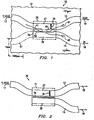
- FIGURE 1 is a diagrammatic fragmentary top view of an apparatus 10 which embodies the present invention.
- FIGURE 1 is diagrammatic and thus not to scale, it is nevertheless appropriate to specifically point out that there is a significant difference between the scale of the units for vertical and horizontal dimensions in FIGURE 1, as evident from the exemplary dimensions indicated by double-headed arrows in the lower left portion of FIGURE 1.
- the apparatus 10 has dimensions and indices of refraction which are selected to facilitate use with near infrared radiation of the type commonly used in the telecommunications industry.
- the present invention is not limited to the infrared portion of the electromagnetic spectrum.
- the apparatus 10 includes a cladding material 12, which has embedded in it two elongate segments 13 and 14 made of a core material.
- the cladding material 12 has an index of refraction which is different from the index of refraction of the core material used for the segments 13 and 14, such that the segments 13 and 14 each function as a respective waveguide for radiation.
- the cross-sectional shape of the segments 13 and 14 is not visible in FIGURE 1, these segments each have a cross-sectional shape which is approximately a square.
- the cladding material 12 is needed in combination the core material of either segment 13 or segment 14 in order to define a waveguide.
- the following discussion will refer to each of the segments 13 and 14 as a waveguide, without specifically referring to the associated cladding material 12.
- the apparatus 10 of FIGURE 1 functions as a passive optical demultiplexer, which may also be referred to as an optical drop multiplexer.
- the arrow 17 at the left of FIGURE 1 represents an optical input signal which is supplied to the waveguide 13, and which includes three optical component signals at respective wavelengths of ⁇ 1, ⁇ 2 and ⁇ 3.
- This signal may, for example, be a signal of the type which is known in the art as a dense wavelength division multiplexing (DWDM) signal.
- DWDM dense wavelength division multiplexing
- the signal at 17 is described here for convenience as having three component signals, it will be recognized that it could have a larger or smaller number of component signals.
- the apparatus 10 separates the component signal at wavelength ⁇ 1 from the component signals at all other wavelengths, in a manner described below, so that the component signal with wavelength ⁇ 1 is routed to travel through the waveguide 14, as indicated by arrow 19, while the other component signals with wavelengths ⁇ 2 and ⁇ 3 are both routed to continue traveling through the waveguide 13, as indicated by arrow 18.
- the apparatus 10 includes a portion 26 which is referred to as a coupling portion, and which is identified diagrammatically by a broken line in FIGURE 1.
- the waveguides 13 and 14 each have a respective portion which is disposed within the coupling portion 26, and these portions are respectively identified by reference numerals 27 and 28 in FIGURE 1. It will be noted that the waveguides 13 and 14 are routed so that the portions 27 and 28 thereof extend parallel to each other, and are relatively close to each other. In contrast, the remaining portions of the waveguides 13 and 14 in FIGURE 1 are spaced from each other by greater distances.
- the portions 27 and 28 of the waveguides are parallel and sufficiently close for a sufficient distance so that radiation traveling through either of the waveguides 13 and 14 will tend to be coupled over in the other thereof, and then back into the original waveguide.
- the cladding material 12 disposed between the portions 27 and 28 of the waveguides, it is not enough to have any significant effect in preventing radiation from passing between the portions 27 and 28. In fact, by appropriate selection of the distance that portions are adjacent, and the spacing between them, 100% of the radiation in waveguide 13 will be coupled over into waveguide 14, and then back into waveguide 13.
- a Bragg grating 36 is provided within the waveguide 13, at a location three-quarters of the way along the portion 27 in the direction of travel of radiation through the waveguide 13.
- the grating 36 is of a known type, and in the embodiment of FIGURE 1 is configured so as to be nontransmissive to radiation at wavelength ⁇ 1, and transmissive to radiation at other wavelengths.
- the components at all wavelengths are coupled at 42 to cross from the waveguide 13 over into the waveguide 14. Due to the lengths of the portions 27 and 28, these components would all normally tend to be subsequently coupled to cross at 46 from the waveguide 14 back into the waveguide 13.
- the grating 36 is nontransmissive to radiation at wavelength ⁇ 1, but is transmissive to other wavelengths. Consequently, the grating 36 is effectively transparent to the signal components at wavelengths ⁇ 2 and ⁇ 3, and these components are coupled to cross at 46 from the waveguide 14 back into the waveguide 13, where at 47 they continue propagating through the waveguide 13.
- the Bragg grating 36 is nontransmissive to the signal component at wavelength ⁇ 1, the grating 36 frustrates coupling at 46 for the component at wavelength ⁇ 1, and this component therefore does not cross from the waveguide 14 back into the waveguide 13, but instead continues traveling through the waveguide 14, as indicated at 48. Consequently, at the right side of FIGURE 1, arrow 18 indicates that the signal components with wavelengths ⁇ 2 and ⁇ 3 end up traveling through the waveguide 13, whereas arrow 19 indicates that the signal component at wavelength ⁇ 1 ends up traveling through the waveguide 14.
- the waveguide 14 is depicted in FIGURE 1 as having an end surface at 56, which represents the beginning of the portion 28 of the waveguide 14 within the coupling portion 26. However, it would be possible for the waveguide 14 to include a further portion, which extends off to the left of the portion 28 thereof, as indicated diagrammatically by a broken line at 57. However, this further portion 57 would not affect the operation of the apparatus 10.
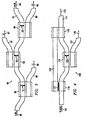
- FIGURE 2 is a diagrammatic fragmentary top view of an apparatus 70 which is an alternative embodiment of the apparatus 10 of FIGURE 1.
- the apparatus 70 includes all of the structure from the apparatus 10, and the same reference numerals are used to designate certain components which are identical.
- the apparatus 70 includes cladding material which is equivalent to that shown at 12 in FIGURE 1, but this cladding material has been omitted from FIGURE 2 for clarity.
- the apparatus 70 includes a coupling portion 71 which is different from the coupling portion 26 of the apparatus 10.
- the coupling portion 71 includes a region 72 which is disposed between the portions 27 and 28 of the waveguides 13 and 14, and which contains a liquid crystal material.
- the liquid crystal region 72 serves as a switching section, and can be selectively switched between two states in a known manner by a not-illustrated control circuit of a known type. In each of these two states, the liquid crystal region 72 has a respective different index of refraction. As a result, the liquid crystal region 72 is respectively transmissive and nontransmissive to all wavelengths of interest in these respective states.
- the region 72 is a liquid crystal material in the disclosed embodiment, it could alternatively be some other electro-optic switching material, such as lithium niobate. If a lithium niobate was used for the switching section 72, the switching section could provide a response time on the order of one microsecond, or faster.
- an optical input signal 17 includes three components at respective wavelengths ⁇ 1, ⁇ 2 and ⁇ 3, the coupling portion 71 will effect routing of these components in a manner so that the component at wavelength ⁇ 1 ends up traveling through waveguide 14, as indicated by arrow 19, and the components at wavelengths ⁇ 2. and ⁇ 3 end up traveling through the waveguide 13; as indicated by arrow 18.
- the components of signal 17 at all wavelengths ⁇ 1, ⁇ 2 and ⁇ 3 will be prevented from being coupled from the portion 27 over to the portion 28. They will therefore all attempt to continue propagating through the portion 27 of the waveguide 13. Since the grating 36 is transmissive to the components at wavelengths ⁇ 2 and ⁇ 3, they will continue traveling through the waveguide 13, as indicated by arrow 18. But since the grating 36 is nontransmissive to the component at wavelength ⁇ 1, this component will not continue traveling along the waveguide 13, and also cannot enter the waveguide 14, because of the current state of the liquid crystal region 72.
- the component at wavelength ⁇ 1 will not propagate rightwardly through either of the waveguides 13 and 14, and thus will not appear at either 18 or 19. Instead, it will be reflected and travel back through the waveguide 13 in the opposite direction, or in other words to the left in FIGURE 2.
- the components at wavelengths ⁇ 2 and ⁇ 3 will always be routed through the waveguide 13, regardless of which state the liquid crystal region 72 is in, and will always appear at 18. Further, the component at wavelength ⁇ 1 will always be separated out from other components, but will only continue propagating through waveguide 14 and appear at 19 when the liquid crystal region 72 is in its transmissive state. The component at wavelength ⁇ 1 will not appear at either of the outputs 18 or 19 when the liquid crystal region 72 is in its nontransmissive state.
- the apparatus 70 of FIGURE 2 not only separates the component at wavelength ⁇ 1 from components at other wavelengths, but also serves as a switch which can enable and disable transmission of the component at wavelength ⁇ 1 to an output of the apparatus 70.
- the left half of the liquid crystal region 72 in FIGURE 2 would be omitted.
- radiation components at all wavelengths would be coupled from the portion 27 of the waveguide 13 over into the portion 28 of the waveguide 14.
- the component at wavelength ⁇ 1 will then always continue on through the waveguide 14 so as to appear at 19, because the grating 36 would prevent it from ever being coupled back into the waveguide 13 under any circumstances.
- the modified liquid crystal region 72 was in its transmissive state, the components at wavelengths ⁇ 2 and ⁇ 3 would be coupled from the portion 28 back into the portion 27, and would then continue through waveguide 13 so as to appear at 18, in a manner comparable to that described above in association with FIGURE 1. In contrast, if the modified liquid crystal region 72 was in its nontransmissive state, the components at wavelengths ⁇ 2 and ⁇ 3 would be prevented from being coupled from the portion 28 back into the portion 27, and would instead continue on through the waveguide 14 with the component at wavelength ⁇ 1, so that all three components would appear together at 19.
- FIGURE 3 is a diagrammatic fragmentary top view similar to FIGURE 1, but showing an apparatus 80 which is still another alternative embodiment of the apparatus 10.
- the apparatus 80 includes cladding material comparable to that shown at 12 in FIGURE 1, but this cladding material has been omitted in FIGURE 3 for clarity.
- the apparatus 80 shown how several arrangements of the type shown in FIGURE 1 can be cascaded in series.
- the apparatus 80 includes a main waveguide 81, which has three coupling portions 82-84 at spaced locations along the length thereof.
- Each of the coupling portions 82-84 is structurally and functionally equivalent to the coupling portion which is shown at 26 in FIGURE 1.
- the apparatus 80 includes three further waveguides 86-88, which each are associated with a respective one of the coupling portions 82-84.
- the coupling portions 82-84 each include one of three Bragg gratings 91-93, which are disposed within the main waveguide 81 at spaced locations therealong.
- the gratings 91-93 are configured to affect respective different wavelengths.
- the grating 91 is configured to be nontransmissive to radiation at wavelength ⁇ 1, and transmissive to other wavelengths.
- the grating 92 is configured to be nontransmissive to radiation at wavelength ⁇ 2, and transmissive to other wavelengths.
- the grating 93 is configured to be nontransmissive to radiation at wavelength ⁇ 3, and transmissive to other wavelengths.
- an input signal 95 is introduced into the main waveguide 81, and includes components at a respective wavelengths ⁇ 1, ⁇ 2, ⁇ 3, ⁇ 4 and ⁇ 5, the coupling portion 82 will separate out the component at wavelength ⁇ 1, by routing it into waveguide 86, so that it appears at 96.
- the remaining components at wavelengths ⁇ 2- ⁇ 5 will be routed by the coupling portion 82 to continue traveling through the waveguide 81 to the coupling portion 83.
- the coupling portion 83 will cause the component at wavelength ⁇ 2 to be routed into the waveguide 87, so that it appears at 97.
- the remaining components at wavelengths ⁇ 3- ⁇ 5 will be routed by the coupling portion 83 to continue traveling through the main waveguide 81 to the coupling portion 84.
- the coupling portion 84 will route the component at wavelength ⁇ 3 into the waveguide 88, so that it appears at 98.
- the remaining signal components at wavelengths ⁇ 4 and ⁇ 5 will be routed by the coupling portion 84 to continue traveling along the main waveguide 81, as indicated at 99.
- FIGURE 4 is a diagrammatic fragmentary top view of an apparatus 110 which is yet another alternative embodiment of the apparatus 10 of FIGURE 1.
- the apparatus 110 of FIGURE 4 includes cladding material comparable to that shown at 12 in FIGURE 1, but this cladding material has been omitted in FIGURE 4 for clarity.
- the apparatus 110 of FIGURE 4 includes a main waveguide 111, which has three successive coupling portions 116, 117 and 118 disposed at spaced locations therealong.
- the coupling portion 117 is associated with a further waveguide 121, and is structurally and functionally equivalent to the coupling portion shown at 26 in FIGURE 1.
- It includes a Bragg grating 122 which is disposed within the waveguide 111.
- the coupling portions 116 and 118 are each somewhat different from the coupling portion 117. They are each associated with a respective end of a further waveguide 126.
- the coupling portions 116 and 118 each lack a Bragg grating or equivalent structure.
- the coupling portions 116 and 118 each have a length in a direction of travel of radiation which is less than the length of the coupling portion 117.
- the coupling portion 116 is long enough to permit radiation to be coupled from the waveguide 111 into the waveguide 126, but is not long enough to permit that radiation to then be coupled from the waveguide 126 back into the waveguide 111.
- the coupling portion 118 is long enough to permit radiation from the waveguide 126 to be coupled into the waveguide 111, but is not long enough to permit that radiation to be subsequently coupled from the waveguide 111 back into the waveguide 118.
- the coupling portion 116 has, between the waveguides 111 and 126, a liquid crystal region 127 which is equivalent to the liquid crystal region 72 discussed above in association with FIGURE 2.
- it can be electrically switched by a not-illustrated control circuit between two different states, in which it is respectively transmissive and nontransmissive to radiation at all wavelengths of interest.
- Coupling portion 117 will separate and route the various signal components in a manner equivalent to that discussed above for the coupling portion 26 of FIGURE 1, such that the component at wavelength ⁇ 1 is routed to travel through the waveguide 121, as indicated by arrow 132, and the remaining components at wavelengths ⁇ 2 and ⁇ 3 are routed to travel through the waveguide 111, as indicated at 133.
- the liquid crystal region 127 is now switched by the not-illustrated control circuit to its transmissive state.
- the coupling portion 116 will now cause all of the components at wavelengths ⁇ 1- ⁇ 3 to be coupled into and propagate through the waveguide 126, such that they bypass the coupling portion 117.
- these component signals reach the coupling portion 118, they will all be coupled from the waveguide 126 back into the waveguide 111, and thus these components at wavelengths ⁇ 1- ⁇ 3 will all appear at 133. Since none of these components reach the coupling portion 117, none of these components will be routed into the waveguide 121, and thus none of them will be present at 132.
- the apparatus 110 of FIGURE 4 thus serves as a switch having first and second states.
- the signal component at wavelength ⁇ 1 is separated out and appears at 132, while signal components at all other wavelengths appear at 133.
- the second state all three component signals at wavelengths ⁇ 1, ⁇ 2 and ⁇ 3 appear at 133, and no component signal appears at 132.
- FIGURE 5 is a diagrammatic fragmentary top view of an apparatus 150 which is still another alternative embodiment of the apparatus 10 of FIGURE 1.
- the apparatus 150 includes cladding material comparable to that shown at 12 in FIGURE 1, but the cladding material has been omitted in FIGURE 5 for clarity.
- the apparatus 150 includes a main waveguide 151, and a coupling portion 152 which can effect coupling between the waveguide 151 and a further waveguide 156.
- the waveguide 156 has a length which is equivalent to the length of the coupling section 152.
- a further coupling portion 157 can effect coupling between the waveguide 156 and a further waveguide 158.
- the coupling portion 156 is structurally and functionally equivalent to the coupling portion 26 of FIGURE 1, and includes a Bragg grating 161 which is equivalent to the grating shown at 36 in FIGURE 1.
- the other coupling portion 157 has an effective length in the direction of the waveguides which is long enough to permit radiation traveling in the waveguide 1'56 to be coupled over into the waveguide 157, but which is too short to permit that radiation to thereafter be coupled back into the waveguide 156.
- an optical signal is introduced into the left end of waveguide 151, and has three components at respective wavelengths ⁇ 1, ⁇ 2 and ⁇ 3.
- the coupling portion 152 effects routing of component signals in a manner comparable to that described above for the coupling portion 26 of FIGURE 1.
- the component signals at wavelengths ⁇ 1 and ⁇ 2 are coupled over into the waveguide 156, and then back into the waveguide 151, whereas the component at wavelength ⁇ 1 is coupled from the waveguide 151 over into the waveguide 156, but is prevented by the grating 161 from being coupled back into the waveguide 151.
- the component at wavelength ⁇ 1 continues propagating within the waveguide 156 until it reaches the coupling portion 157, where it is coupled from the waveguide 156 over into the waveguide 158.
- the component at wavelength ⁇ 1 ends up traveling through the waveguide 158, as indicated by arrow 163, and the components at wavelengths ⁇ 2- ⁇ 3 end up traveling through the waveguide 151, as indicated by arrow 164.
- FIGURE 6 is a diagrammatic fragmentary top view of an apparatus 210 which is yet another alternative embodiment of the apparatus 10 of FIGURE 1.
- the apparatus 210 includes cladding material similar to that shown at 12 in FIGURE 1, but the cladding material has been omitted in FIGURE 6 for clarity.
- the apparatus 210 of FIGURE 6 is a device of a type commonly known as an optical add/drop multiplexer (OADM).
- the apparatus 210 includes a main waveguide 211, and two coupling portions 213 and 214 which are provided at spaced locations along the waveguide 211.
- the coupling portion 213 can effect coupling between the waveguide 211 and a further waveguide 217.
- the coupling portion 213 is structurally and functionally equivalent to the coupling portion shown at 26 in FIGURE 1. In this regard, it includes a Bragg grating 218 disposed within the waveguide 211.
- the other coupling portion 214 can effect coupling between the waveguide 211 and yet another waveguide 223.
- the waveguide 223 has an end surface at the right end of the coupling portion 214 in FIGURE 6, and has a short distance from this end surface a Bragg grating 222.
- the Brag grating 222 is non-transmissive to radiation at a wavelength ⁇ 4, and is transmissive to radiation at other wavelengths.
- the coupling portion 214 has a length which is sufficient to permit radiation traveling in the waveguide 211 to be coupled over into the waveguide 223 and then back into the waveguide 211, but which is too short to permit that radiation to thereafter be coupled again from the waveguide 211 back into the waveguide 223.
- the coupling portion 213 may optionally include between the waveguides 211 and 217 a liquid crystal region 219 comparable to the liquid crystal region 72 of FIGURE 2.
- the coupling portion 214 may optionally include between the waveguides 211 and 223 a liquid crystal region 224 which is comparable to the liquid crystal region 72 of FIGURE 2.
- the liquid crystal regions 219 and 224 are both omitted from the apparatus 210.
- an optical signal is introduced into the left end of the waveguide 211, and has three components at respective wavelengths of ⁇ 1 , ⁇ 2 and ⁇ 3 This optical signal travels through the waveguide 211 until it reaches the coupling portion 213, where the various components are routed in a manner comparable to that described above for the coupling portion 26 of FIGURE 1.
- the component at wavelength ⁇ 1 is coupled from the waveguide 211 over into the waveguide 217 and is then prevented from being coupled back into the waveguide 211 by the grating 218.
- the grating 218 is transmissive to other wavelengths, the components at wavelengths ⁇ 2 and ⁇ 3 are coupled from the waveguide 211 into the waveguide 217, and then from the waveguide 217 back into the waveguide 211, and thereafter continue along the waveguide 211 to the coupling portion 214.
- An optical signal indicated by arrow 233 has a wavelength ⁇ 4 , and is traveling through the waveguide 223.
- this optical signal is coupled from the waveguide 223 over into the waveguide 211, and would then tend to be coupled from the waveguide 211 back over into the waveguide 223, but the Bragg grating 222 will prevent the radiation at wavelength ⁇ 4 from being coupled back into the waveguide 223.
- waveguide 211 ends up carrying the components at wavelengths ⁇ 2, ⁇ 3 and ⁇ 4, as indicated by arrow 234.
- the waveguide 223 carries only one signal at wavelength ⁇ 4, it will be recognized that the waveguide 223 could alternatively carry several component signals at respective different wavelengths, and that all of these components could be coupled over into the waveguide 211. In that case, additional Bragg gratings would be provided within the waveguide 223 adjacent the Bragg grating 222, each Bragg grating in the waveguide 223 being non-transmissive to radiation at a respective different wavelength introduced into the waveguide 223 at 233.
- liquid crystal region 219 is provided in the coupling portion 213, it can be used to selectively control whether or not the component signal at wavelength ⁇ 1 is routed into the waveguide 217 and appears at 232.
- liquid crystal region 224 is provided in the coupling portion 214, it can be used to selectively control whether or not the component signal at wavelength ⁇ 4 is coupled from the waveguide 223 over into the waveguide 211, and thus whether or not this component signal appears at 234.
- FIGURE 7 is a diagrammatic fragmentary top view of an apparatus 250 which is still another alternative embodiment of apparatus 10 of FIGURE 1.
- the apparatus 250 includes cladding material comparable to that shown at 12 in FIGURE 1, but the cladding material has been omitted in FIGURE 7 for clarity.
- the apparatus 250 includes two waveguides 251 and 252, and a coupling portion 256 which effects coupling between respective portions of the two waveguides 251 and 252.
- the coupling portion 256 appears to be similar to the coupling portion 26 of FIGURE 1. However, there are two significant differences.
- the coupling portion 256 includes a Bragg grating 257
- the grating 257 is not provided within the waveguide 251 through which radiation travels to the coupling portion 256, but instead is in other waveguide 252.
- the grating 257 is configured to be nontransmissive to radiation at wavelength ⁇ 1, and to be transmissive to radiation at other wavelengths, including wavelengths ⁇ 2 and ⁇ 3.
- a second difference is that the coupling portion 256 has a length in the direction of travel of radiation which is long enough to permit coupling of radiation from the waveguide 251 over into the waveguide 252, but is too short to permit that radiation to be coupled from the waveguide 252 back into the waveguide 251.
- the grating 257 is transmissive to the component signals at wavelengths ⁇ 2 and ⁇ 3, and these component signals will thus be coupled from the waveguide 251 over into the waveguide 252 within the coupling portions 256.
- the coupling portion 256 is too short for them to thereafter be coupled back into the waveguide 251, they will continue on through the waveguide 252, as indicated by arrow 263.
- FIGUREs 8-10 are diagrammatic sectional views showing successive steps in a inexpensive process for making the apparatus 10 of FIGURE 1.
- the sectional view of FIGURE 10 corresponds to the section line 10-10 in FIGURE 1.
- a planar substrate 301 is provided, and is made of a glass or polymer material of a type known to persons skilled in the art.
- the substrate 301 has an index of refraction which would be suitable for the cladding material 12 of FIGURE 1, because the substrate 301 will ultimately become part of the cladding material, as discussed below.
- a layer 302 is then formed on top of the substrate 301, for example through deposition or by spinning it on.
- the layer 302 is made of a glass or polymer material of a type known to persons skilled in the art.
- the layer 302 has an index of refraction which would be suitable for the core material of the waveguides 13 and 14 of FIGURE 1, because the waveguides 13 and 14 will be formed from the layer 302, as discussed below.
- a patterned etch using known techniques is carried out on the layer 302, in order to selectively remove material of the layer 302 other than the portions thereof which will serve as the waveguides 13 and 14. Following this etch procedure, the waveguides 13 and 14 are left on top of the substrate 301, as shown in FIGURE 9.
- patterned photolithography is carried out on the waveguide 13 using a technique well known in the art, in order to form therein the Bragg grating 36 (FIGURE 1).
- This known technique involves applying a photomask and then directing radiation from an ultraviolet laser onto the waveguide 13 through the mask, the mask distributing the laser light in a periodic way that changes molecular bonds in the core material so as to produce the grating 36.
- a cladding overcoat 306 is applied over the structure shown in FIGURE 9, in order to obtain the apparatus 10 shown in FIGURE 10.
- the cladding overcoat 306 may be applied through deposition, or by spinning it on.
- the overcoat 306 is made of the same material as the substrate 301.
- the substrate 301 and overcoat 306 thus together serve as cladding 12 (FIGURE 1) for the core material which serves as the waveguides 13 and 14.
- FIGURES 11-13 are diagrammatic sectional view showing successive steps in an inexpensive process which is an alternative embodiment of the process discussed above in association with FIGURES 8-10.
- FIGURE 11 shows a glass or polymer substrate 320, which can be made of the same material discussed above for use as the layer 301 in FIGURE B.
- the substrate 320 thus has characteristics, including an appropriate index of refraction, that make it suitable for use as a cladding material.
- Grooves 321 and 322 are formed therein, so as to open into the substrate 320 from a top surface thereof.
- the grooves 321 and 322 correspond in size and shape to the waveguides shown at 13 and 14 in FIGURE 1.
- the grooves 321 and 322 are formed by etching the substrate 320, or by embossing the top surface of the substrate 320 in association with the application of heat, for example through a hot rolling process.
- the grooves 321 and 322 in the substrate 320 are filled with a different glass or polymer material, which can be the same material discussed above for use as the layer 302 in FIGURE 8.
- the glass or polymer material in the grooves 321 and 322 thus has characteristics, including an appropriate index of refraction, which make it suitable for use as the core material of a waveguide, and in fact the material in the grooves 321 and 322 will serve as the waveguides 13 and 14.
- the top surface of the resulting structure may be planarized using a known planarization technique, in order to remove any excess core material which is not disposed within the grooves.
- the Bragg grating 36 (FIGURE 1) is formed within the waveguide 13 using patterned photolithography, in a manner similar to that described above in association with FIGURE 9. Then, a cladding overcoat 326 is applied over the resulting structure, as shown in FIGURE 13.
- the overcoat 326 is the same glass or polymer material as the substrate 320, and can be applied through deposition, or by spinning it on. The substrate 320 and overcoat 326 together serve as cladding for the core material that serves as the waveguides 13 and 14.
- an optical input or output fiber can be coupled directly to any of the disclosed waveguides, for example by simply fusing it to an end of the core material of that waveguide using a known laser fusing technique. This avoids the need to use collimating optics or other complex optical or mechanical assemblies.
- the present invention provides a number of technical advantages.
- One such technical advantage is the provision of a simple approach for using waveguides in combination with structure such as Bragg gratings to effect wavelength separation. This facilitates use of technologies such as dense wavelength division multiplexing (DWDM), while avoiding problems of complexity and alignment that are present in other existing approaches.
- DWDM dense wavelength division multiplexing
- the complexity and alignment issues in existing arrangements also tend to cause relatively high optical losses, whereas the present invention is not only simple, but permits optical losses be minimized.
- a further advantage is that the present invention performs all processing directly on optical signals, thereby avoiding any need to convert optical signals to electrical signal, process the electrical signals, and then convert the electrical signals back into optical signals. Conversions between electrical and optical signals are slow, and by avoiding these conversions the invention provides faster throughput.
- a further advantage of the present invention results from the use of switching sections made from electro-optical materials such as liquid crystal material, lithium niobate, or the like, which permit processing of optical signals to be carried out in a selective manner, for example to implement addressable or reconfigurable optical routers or add/drop multiplexers.
- the present invention can achieve a relatively fast response time of approximately one microsecond or less, which is significantly faster than certain other existing techniques for optical switching, such as those which use bubbles, micro-electro-opto-mechanical devices (MEMS), or liquid crystal material with a different opto-mechanical structure.
- MEMS micro-electro-opto-mechanical devices
Landscapes
- Physics & Mathematics (AREA)
- General Physics & Mathematics (AREA)
- Optics & Photonics (AREA)
- Engineering & Computer Science (AREA)
- Microelectronics & Electronic Packaging (AREA)
- Nonlinear Science (AREA)
- Chemical & Material Sciences (AREA)
- Crystallography & Structural Chemistry (AREA)
- Electromagnetism (AREA)
- Computer Networks & Wireless Communication (AREA)
- Signal Processing (AREA)
- Optical Integrated Circuits (AREA)
Abstract
Description
- This invention relates in general to communication with optical signals and, more particularly, to a method and apparatus for facilitating communication using optical signals which include multiple signal components that each have a respective different wavelength.
- Telecommunications is a field which has been rapidly evolving over the past twenty years, fueled in part by the progressively increasing popularity of technologies such as cellular telephones, facsimile machines, and computer communications that use the Internet. Due to these growing new technologies, there has been a progressively increasing demand for telecommunications equipment with greater information-carrying capacity, which in turn has created a progressively increasing focus on effecting communications through the use of optical signals.
- Through use of existing techniques such as dense wavelength division multiplexing (DWDM), a single optical fiber in a telecommunications system will frequently be carrying many component optical signals at respective different wavelengths, and each such component optical signal will be a time division multiplexed (TDM) signal that carries a number of separate telephone conversations or other ongoing communications. To the extent that optical signals are being used in this manner to transmit large amounts of information, techniques are needed for efficiently and cheaply processing optical signals, including demultiplexing of optical signals, multiplexing of optical signals, and switching of optical signals.
- Many existing techniques for processing optical signals involve assemblies which are complex and which present difficult alignment problems that can produce relatively high optical losses. Other systems convert the optical data into electrical signals, subsequently carry out processing of the electrical signals to effect steps such as multiplexing, demultiplexing and switching, and then convert the electrical signals back into optical signals. The equipment used to effect these conversions introduces a significant delay into handling of the signals. All of these approaches are relatively expensive.
- Some consideration has been given to fusing optical fibers in order to eliminate certain coupling or collimating optics, but the resulting devices are generally difficult to produce. Consideration has also been given to optical switches that use liquid crystals, bubbles, or micro-electro-opto-mechanical devices (MEMS), but these arrangements have relatively slow response times, on the order of a few milliseconds, and typically require a number of optical components that make them relatively complex and expensive, and that tend to result in relatively high optical losses.
- From the foregoing, it may be appreciated that a need has arisen for a method and apparatus for processing optical signals, which avoid at least some of the problems discussed above. According to a first from of the present invention, a method and apparatus are provided to address this need, and involve first and second waveguides, and a coupling portion operable to cause radiation at a first wavelength which is traveling in a direction of travel through the first waveguide and which reaches the coupling portion to be routed so as to be traveling in one of the first and second waveguides when exiting the coupling portion, and to cause radiation at a second wavelength different from the first wavelength which is traveling through the first waveguide in the direction of travel and which reaches the coupling portion to be routed so as to be traveling in the other of the first and second waveguides when exiting the coupling portion. The coupling portion includes the first and second waveguides respectively having first and second portions that extend approximately parallel to each other and that are sufficiently close for a sufficient distance to permit coupling therebetween of radiation having at least one of the first and second wavelengths, and includes structure operable along at least part of the distance to frustrate coupling between the first and second portions of radiation having one of the first and second wavelengths while permitting coupling between the first and second portions of radiation having the other of the first and second wavelengths.
- According to another form of the invention, a method involves: providing a first layer made of a material which has a first index of refraction; forming on the first layer first and second elongate sections made of a second material which is transmissive to radiation of a predetermined wavelength and which has a second index of refraction different from the first index of refraction; and forming over the elongate sections and exposed portions of the first layer a third layer made of a material which has a third index of refraction different from the second index of refraction, wherein the elongate sections function as cores of respective waveguides, and the materials of the first and second layers function as cladding for the cores.
- A better understanding of the present invention will be realized from the detailed description which follows, taken in conjunction with the accompanying drawings, in which:
- FIGURE 1 is diagrammatic fragmentary top view of an apparatus which embodies the present invention, and which processes optical signals;
- FIGURE 2 is a diagrammatic fragmentary top view of an apparatus which is an alternative embodiment of the apparatus of FIGURE 1;
- FIGURE 3 is a diagrammatic fragmentary top view of an apparatus which is a further alternative embodiment of the apparatus of FIGURE 1;
- FIGURE 4 is a diagrammatic fragmentary top view of an apparatus which is still another alternative embodiment of the apparatus of FIGURE 1;
- FIGURE 5 is a diagrammatic fragmentary top view of an apparatus which is yet another alternative embodiment of the apparatus of FIGURE 1;
- FIGURE 6 is a diagrammatic fragmentary top view of a an apparatus which is a further alternative embodiment of the apparatus of FIGURE 1;
- FIGURE 7 is a diagrammatic fragmentary top view of an apparatus which is yet another alternative embodiment of the apparatus of FIGURE 1;
- FIGUREs 8-10 are diagrammatic sectional views that show successive steps in a process which embodies the present invention and which can be used to fabricate the apparatus of FIGURE 1; and
- FIGUREs 11-13 are diagrammatic sectional views that show successive steps in a different process which embodies the present invention and which can be used to fabricate the apparatus of FIGURE 1.
- FIGURE 1 is a diagrammatic fragmentary top view of an
apparatus 10 which embodies the present invention. Although FIGURE 1 is diagrammatic and thus not to scale, it is nevertheless appropriate to specifically point out that there is a significant difference between the scale of the units for vertical and horizontal dimensions in FIGURE 1, as evident from the exemplary dimensions indicated by double-headed arrows in the lower left portion of FIGURE 1. Also, theapparatus 10 has dimensions and indices of refraction which are selected to facilitate use with near infrared radiation of the type commonly used in the telecommunications industry. However, it will be recognized that the present invention is not limited to the infrared portion of the electromagnetic spectrum. - The
apparatus 10 includes acladding material 12, which has embedded in it twoelongate segments cladding material 12 has an index of refraction which is different from the index of refraction of the core material used for thesegments segments segments - Technically, the
cladding material 12 is needed in combination the core material of eithersegment 13 orsegment 14 in order to define a waveguide. For convenience, however, the following discussion will refer to each of thesegments cladding material 12. - The
apparatus 10 of FIGURE 1 functions as a passive optical demultiplexer, which may also be referred to as an optical drop multiplexer. In this regard, thearrow 17 at the left of FIGURE 1 represents an optical input signal which is supplied to thewaveguide 13, and which includes three optical component signals at respective wavelengths of λ1, λ2 and λ3. This signal may, for example, be a signal of the type which is known in the art as a dense wavelength division multiplexing (DWDM) signal. Although the signal at 17 is described here for convenience as having three component signals, it will be recognized that it could have a larger or smaller number of component signals. - The
apparatus 10 separates the component signal at wavelength λ1 from the component signals at all other wavelengths, in a manner described below, so that the component signal with wavelength λ1 is routed to travel through thewaveguide 14, as indicated byarrow 19, while the other component signals with wavelengths λ2 and λ3 are both routed to continue traveling through thewaveguide 13, as indicated byarrow 18. - In more detail, the
apparatus 10 includes aportion 26 which is referred to as a coupling portion, and which is identified diagrammatically by a broken line in FIGURE 1. Thewaveguides coupling portion 26, and these portions are respectively identified byreference numerals waveguides portions waveguides - The
portions waveguides cladding material 12 disposed between theportions portions waveguide 13 will be coupled over intowaveguide 14, and then back intowaveguide 13. - A Bragg
grating 36 is provided within thewaveguide 13, at a location three-quarters of the way along theportion 27 in the direction of travel of radiation through thewaveguide 13. Thegrating 36 is of a known type, and in the embodiment of FIGURE 1 is configured so as to be nontransmissive to radiation at wavelength λ1, and transmissive to radiation at other wavelengths. - Consequently, as the optical signal with components at respective wavelengths λ1, λ2 and λ3 is traveling through the
waveguide 13, as indicated at 41, the components at all wavelengths are coupled at 42 to cross from thewaveguide 13 over into thewaveguide 14. Due to the lengths of theportions waveguide 14 back into thewaveguide 13. However, as noted above, thegrating 36 is nontransmissive to radiation at wavelength λ1, but is transmissive to other wavelengths. Consequently, thegrating 36 is effectively transparent to the signal components at wavelengths λ2 and λ3, and these components are coupled to cross at 46 from thewaveguide 14 back into thewaveguide 13, where at 47 they continue propagating through thewaveguide 13. - In contrast, since the Bragg
grating 36 is nontransmissive to the signal component at wavelength λ1, thegrating 36 frustrates coupling at 46 for the component at wavelength λ1, and this component therefore does not cross from thewaveguide 14 back into thewaveguide 13, but instead continues traveling through thewaveguide 14, as indicated at 48. Consequently, at the right side of FIGURE 1,arrow 18 indicates that the signal components with wavelengths λ2 and λ3 end up traveling through thewaveguide 13, whereasarrow 19 indicates that the signal component at wavelength λ1 ends up traveling through thewaveguide 14. - The
waveguide 14 is depicted in FIGURE 1 as having an end surface at 56, which represents the beginning of theportion 28 of thewaveguide 14 within thecoupling portion 26. However, it would be possible for thewaveguide 14 to include a further portion, which extends off to the left of theportion 28 thereof, as indicated diagrammatically by a broken line at 57. However, thisfurther portion 57 would not affect the operation of theapparatus 10. - FIGURE 2 is a diagrammatic fragmentary top view of an
apparatus 70 which is an alternative embodiment of theapparatus 10 of FIGURE 1. Theapparatus 70 includes all of the structure from theapparatus 10, and the same reference numerals are used to designate certain components which are identical. Theapparatus 70 includes cladding material which is equivalent to that shown at 12 in FIGURE 1, but this cladding material has been omitted from FIGURE 2 for clarity. - The only significant difference between the
apparatus 70 of FIGURE 2 and theapparatus 10 of FIGURE 1 is that theapparatus 70 includes acoupling portion 71 which is different from thecoupling portion 26 of theapparatus 10. In particular, thecoupling portion 71 includes aregion 72 which is disposed between theportions waveguides liquid crystal region 72 serves as a switching section, and can be selectively switched between two states in a known manner by a not-illustrated control circuit of a known type. In each of these two states, theliquid crystal region 72 has a respective different index of refraction. As a result, theliquid crystal region 72 is respectively transmissive and nontransmissive to all wavelengths of interest in these respective states. Although theregion 72 is a liquid crystal material in the disclosed embodiment, it could alternatively be some other electro-optic switching material, such as lithium niobate. If a lithium niobate was used for theswitching section 72, the switching section could provide a response time on the order of one microsecond, or faster. - When the
liquid crystal region 72 is in the state where it is transmissive, coupling is possible between theportions apparatus 70 functions in precisely the same manner as described above for theapparatus 10 of FIGURE 1. In particular, if anoptical input signal 17 includes three components at respective wavelengths λ1, λ2 and λ3, thecoupling portion 71 will effect routing of these components in a manner so that the component at wavelength λ1 ends up traveling throughwaveguide 14, as indicated byarrow 19, and the components at wavelengths λ2. and λ3 end up traveling through thewaveguide 13; as indicated byarrow 18. - On the other hand, if the
liquid crystal region 72 is set to the state where it is nontransmissive to all wavelengths of interest, the components ofsignal 17 at all wavelengths λ1, λ2 and λ3 will be prevented from being coupled from theportion 27 over to theportion 28. They will therefore all attempt to continue propagating through theportion 27 of thewaveguide 13. Since the grating 36 is transmissive to the components at wavelengths λ2 and λ3, they will continue traveling through thewaveguide 13, as indicated byarrow 18. But since the grating 36 is nontransmissive to the component at wavelength λ1, this component will not continue traveling along thewaveguide 13, and also cannot enter thewaveguide 14, because of the current state of theliquid crystal region 72. Therefore, the component at wavelength λ1 will not propagate rightwardly through either of thewaveguides waveguide 13 in the opposite direction, or in other words to the left in FIGURE 2. - Summarizing, the components at wavelengths λ2 and λ3 will always be routed through the
waveguide 13, regardless of which state theliquid crystal region 72 is in, and will always appear at 18. Further, the component at wavelength λ1 will always be separated out from other components, but will only continue propagating throughwaveguide 14 and appear at 19 when theliquid crystal region 72 is in its transmissive state. The component at wavelength λ1 will not appear at either of theoutputs liquid crystal region 72 is in its nontransmissive state. Thus, theapparatus 70 of FIGURE 2 not only separates the component at wavelength λ1 from components at other wavelengths, but also serves as a switch which can enable and disable transmission of the component at wavelength λ1 to an output of theapparatus 70. - In a possible variation of the apparatus of FIGURE 2, which is not separately illustrated, the left half of the
liquid crystal region 72 in FIGURE 2 would be omitted. In that case, radiation components at all wavelengths would be coupled from theportion 27 of thewaveguide 13 over into theportion 28 of thewaveguide 14. The component at wavelength λ1 will then always continue on through thewaveguide 14 so as to appear at 19, because the grating 36 would prevent it from ever being coupled back into thewaveguide 13 under any circumstances. - If the modified
liquid crystal region 72 was in its transmissive state, the components at wavelengths λ2 and λ3 would be coupled from theportion 28 back into theportion 27, and would then continue throughwaveguide 13 so as to appear at 18, in a manner comparable to that described above in association with FIGURE 1. In contrast, if the modifiedliquid crystal region 72 was in its nontransmissive state, the components at wavelengths λ2 and λ3 would be prevented from being coupled from theportion 28 back into theportion 27, and would instead continue on through thewaveguide 14 with the component at wavelength λ1, so that all three components would appear together at 19. - FIGURE 3 is a diagrammatic fragmentary top view similar to FIGURE 1, but showing an apparatus 80 which is still another alternative embodiment of the
apparatus 10. The apparatus 80 includes cladding material comparable to that shown at 12 in FIGURE 1, but this cladding material has been omitted in FIGURE 3 for clarity. The apparatus 80 shown how several arrangements of the type shown in FIGURE 1 can be cascaded in series. - In particular, the apparatus 80 includes a
main waveguide 81, which has three coupling portions 82-84 at spaced locations along the length thereof. Each of the coupling portions 82-84 is structurally and functionally equivalent to the coupling portion which is shown at 26 in FIGURE 1. The apparatus 80 includes three further waveguides 86-88, which each are associated with a respective one of the coupling portions 82-84. The coupling portions 82-84 each include one of three Bragg gratings 91-93, which are disposed within themain waveguide 81 at spaced locations therealong. - The gratings 91-93 are configured to affect respective different wavelengths. In particular, the grating 91 is configured to be nontransmissive to radiation at wavelength λ1, and transmissive to other wavelengths. The grating 92 is configured to be nontransmissive to radiation at wavelength λ2, and transmissive to other wavelengths. The grating 93 is configured to be nontransmissive to radiation at wavelength λ3, and transmissive to other wavelengths.
- If an
input signal 95 is introduced into themain waveguide 81, and includes components at a respective wavelengths λ1, λ2, λ3, λ4 and λ5, thecoupling portion 82 will separate out the component at wavelength λ1, by routing it intowaveguide 86, so that it appears at 96. The remaining components at wavelengths λ2-λ5 will be routed by thecoupling portion 82 to continue traveling through thewaveguide 81 to thecoupling portion 83. Thecoupling portion 83 will cause the component at wavelength λ2 to be routed into thewaveguide 87, so that it appears at 97. The remaining components at wavelengths λ3-λ5 will be routed by thecoupling portion 83 to continue traveling through themain waveguide 81 to thecoupling portion 84. Thecoupling portion 84 will route the component at wavelength λ3 into the waveguide 88, so that it appears at 98. The remaining signal components at wavelengths λ4 and λ5 will be routed by thecoupling portion 84 to continue traveling along themain waveguide 81, as indicated at 99. - FIGURE 4 is a diagrammatic fragmentary top view of an
apparatus 110 which is yet another alternative embodiment of theapparatus 10 of FIGURE 1. Theapparatus 110 of FIGURE 4 includes cladding material comparable to that shown at 12 in FIGURE 1, but this cladding material has been omitted in FIGURE 4 for clarity. Theapparatus 110 of FIGURE 4 includes amain waveguide 111, which has threesuccessive coupling portions coupling portion 117 is associated with afurther waveguide 121, and is structurally and functionally equivalent to the coupling portion shown at 26 in FIGURE 1. It includes a Bragg grating 122 which is disposed within thewaveguide 111. - The
coupling portions coupling portion 117. They are each associated with a respective end of afurther waveguide 126. Thecoupling portions coupling portions coupling portion 117. As a result, thecoupling portion 116 is long enough to permit radiation to be coupled from thewaveguide 111 into thewaveguide 126, but is not long enough to permit that radiation to then be coupled from thewaveguide 126 back into thewaveguide 111. Similarly, thecoupling portion 118 is long enough to permit radiation from thewaveguide 126 to be coupled into thewaveguide 111, but is not long enough to permit that radiation to be subsequently coupled from thewaveguide 111 back into thewaveguide 118. - The
coupling portion 116 has, between thewaveguides liquid crystal region 127 which is equivalent to theliquid crystal region 72 discussed above in association with FIGURE 2. In particular, it can be electrically switched by a not-illustrated control circuit between two different states, in which it is respectively transmissive and nontransmissive to radiation at all wavelengths of interest. - With reference to the
arrow 131 at the left side of FIGURE 4, assume that optical radiation having three components at respective wavelengths λ1, λ2 and λ3 is introduced into the left end of thewaveguide 111. Also assume that theliquid crystal region 127 is in its nontransmissive state. The radiation introduced into thewaveguide 111 at 131 will propagate through thecoupling portion 116 without switching waveguides, and continue through thewaveguide 111 until it reaches thecoupling portion 117. Couplingportion 117 will separate and route the various signal components in a manner equivalent to that discussed above for thecoupling portion 26 of FIGURE 1, such that the component at wavelength λ1 is routed to travel through thewaveguide 121, as indicated byarrow 132, and the remaining components at wavelengths λ2 and λ3 are routed to travel through thewaveguide 111, as indicated at 133. - Assume that the
liquid crystal region 127 is now switched by the not-illustrated control circuit to its transmissive state. Thecoupling portion 116 will now cause all of the components at wavelengths λ1-λ3 to be coupled into and propagate through thewaveguide 126, such that they bypass thecoupling portion 117. When these component signals reach thecoupling portion 118, they will all be coupled from thewaveguide 126 back into thewaveguide 111, and thus these components at wavelengths λ1-λ3 will all appear at 133. Since none of these components reach thecoupling portion 117, none of these components will be routed into thewaveguide 121, and thus none of them will be present at 132. - The
apparatus 110 of FIGURE 4 thus serves as a switch having first and second states. In the first state, the signal component at wavelength λ1 is separated out and appears at 132, while signal components at all other wavelengths appear at 133. In the second state, all three component signals at wavelengths λ1, λ2 and λ3 appear at 133, and no component signal appears at 132. - FIGURE 5 is a diagrammatic fragmentary top view of an
apparatus 150 which is still another alternative embodiment of theapparatus 10 of FIGURE 1. Theapparatus 150 includes cladding material comparable to that shown at 12 in FIGURE 1, but the cladding material has been omitted in FIGURE 5 for clarity. Theapparatus 150 includes amain waveguide 151, and acoupling portion 152 which can effect coupling between thewaveguide 151 and afurther waveguide 156. Thewaveguide 156 has a length which is equivalent to the length of thecoupling section 152. Afurther coupling portion 157 can effect coupling between thewaveguide 156 and afurther waveguide 158. - The
coupling portion 156 is structurally and functionally equivalent to thecoupling portion 26 of FIGURE 1, and includes a Bragg grating 161 which is equivalent to the grating shown at 36 in FIGURE 1. Theother coupling portion 157 has an effective length in the direction of the waveguides which is long enough to permit radiation traveling in the waveguide 1'56 to be coupled over into thewaveguide 157, but which is too short to permit that radiation to thereafter be coupled back into thewaveguide 156. - With reference to the
arrow 162 at the left side of FIGURE 5, assume that an optical signal is introduced into the left end ofwaveguide 151, and has three components at respective wavelengths λ1, λ2 and λ3. When this optical signal reaches thecoupling portion 152, thecoupling portion 152 effects routing of component signals in a manner comparable to that described above for thecoupling portion 26 of FIGURE 1. In particular, the component signals at wavelengths λ1 and λ2 are coupled over into thewaveguide 156, and then back into thewaveguide 151, whereas the component at wavelength λ1 is coupled from thewaveguide 151 over into thewaveguide 156, but is prevented by the grating 161 from being coupled back into thewaveguide 151. Accordingly, the component at wavelength λ1 continues propagating within thewaveguide 156 until it reaches thecoupling portion 157, where it is coupled from thewaveguide 156 over into thewaveguide 158. Thus, the component at wavelength λ1 ends up traveling through thewaveguide 158, as indicated byarrow 163, and the components at wavelengths λ2-λ3 end up traveling through thewaveguide 151, as indicated byarrow 164. - FIGURE 6 is a diagrammatic fragmentary top view of an
apparatus 210 which is yet another alternative embodiment of theapparatus 10 of FIGURE 1. Theapparatus 210 includes cladding material similar to that shown at 12 in FIGURE 1, but the cladding material has been omitted in FIGURE 6 for clarity. Theapparatus 210 of FIGURE 6 is a device of a type commonly known as an optical add/drop multiplexer (OADM). Theapparatus 210 includes amain waveguide 211, and twocoupling portions waveguide 211. Thecoupling portion 213 can effect coupling between thewaveguide 211 and afurther waveguide 217. Thecoupling portion 213 is structurally and functionally equivalent to the coupling portion shown at 26 in FIGURE 1. In this regard, it includes a Bragg grating 218 disposed within thewaveguide 211. - The
other coupling portion 214 can effect coupling between thewaveguide 211 and yet anotherwaveguide 223. Thewaveguide 223 has an end surface at the right end of thecoupling portion 214 in FIGURE 6, and has a short distance from this end surface a Bragg grating 222. The Brag grating 222 is non-transmissive to radiation at a wavelength λ4, and is transmissive to radiation at other wavelengths. Thecoupling portion 214 has a length which is sufficient to permit radiation traveling in thewaveguide 211 to be coupled over into thewaveguide 223 and then back into thewaveguide 211, but which is too short to permit that radiation to thereafter be coupled again from thewaveguide 211 back into thewaveguide 223. - The
coupling portion 213 may optionally include between thewaveguides 211 and 217 aliquid crystal region 219 comparable to theliquid crystal region 72 of FIGURE 2. Thecoupling portion 214 may optionally include between thewaveguides 211 and 223 aliquid crystal region 224 which is comparable to theliquid crystal region 72 of FIGURE 2. - Assume initially that the
liquid crystal regions apparatus 210. Further, and with reference to thearrow 231 at the left of FIGURE 6, assume that an optical signal is introduced into the left end of thewaveguide 211, and has three components at respective wavelengths of λ1, λ2 and λ3 This optical signal travels through thewaveguide 211 until it reaches thecoupling portion 213, where the various components are routed in a manner comparable to that described above for thecoupling portion 26 of FIGURE 1. In particular, the component at wavelength λ1 is coupled from thewaveguide 211 over into thewaveguide 217 and is then prevented from being coupled back into thewaveguide 211 by thegrating 218. It therefore continues along thewaveguide 217, as indicated byarrow 232. In contrast, since the grating 218 is transmissive to other wavelengths, the components at wavelengths λ2 and λ3 are coupled from thewaveguide 211 into thewaveguide 217, and then from thewaveguide 217 back into thewaveguide 211, and thereafter continue along thewaveguide 211 to thecoupling portion 214. - An optical signal indicated by
arrow 233 has a wavelength λ4, and is traveling through thewaveguide 223. In thecoupling portion 214, this optical signal is coupled from thewaveguide 223 over into thewaveguide 211, and would then tend to be coupled from thewaveguide 211 back over into thewaveguide 223, but the Bragg grating 222 will prevent the radiation at wavelength λ4 from being coupled back into thewaveguide 223. Thus,waveguide 211 ends up carrying the components at wavelengths λ2, λ3 and λ4, as indicated byarrow 234. - Although the foregoing discussion explains that the
waveguide 223 carries only one signal at wavelength λ4, it will be recognized that thewaveguide 223 could alternatively carry several component signals at respective different wavelengths, and that all of these components could be coupled over into thewaveguide 211. In that case, additional Bragg gratings would be provided within thewaveguide 223 adjacent the Bragg grating 222, each Bragg grating in thewaveguide 223 being non-transmissive to radiation at a respective different wavelength introduced into thewaveguide 223 at 233. - In view of the discussion of the liquid crystal regions in preceding embodiments, it will be recognized that, if the
liquid crystal region 219 is provided in thecoupling portion 213, it can be used to selectively control whether or not the component signal at wavelength λ1 is routed into thewaveguide 217 and appears at 232. Similarly, if theliquid crystal region 224 is provided in thecoupling portion 214, it can be used to selectively control whether or not the component signal at wavelength λ4 is coupled from thewaveguide 223 over into thewaveguide 211, and thus whether or not this component signal appears at 234. - FIGURE 7 is a diagrammatic fragmentary top view of an
apparatus 250 which is still another alternative embodiment ofapparatus 10 of FIGURE 1. Theapparatus 250 includes cladding material comparable to that shown at 12 in FIGURE 1, but the cladding material has been omitted in FIGURE 7 for clarity. Theapparatus 250 includes twowaveguides coupling portion 256 which effects coupling between respective portions of the twowaveguides coupling portion 256 appears to be similar to thecoupling portion 26 of FIGURE 1. However, there are two significant differences. - First, although the
coupling portion 256 includes a Bragg grating 257, thegrating 257 is not provided within thewaveguide 251 through which radiation travels to thecoupling portion 256, but instead is inother waveguide 252. The grating 257 is configured to be nontransmissive to radiation at wavelength λ1, and to be transmissive to radiation at other wavelengths, including wavelengths λ2 and λ3. A second difference is that thecoupling portion 256 has a length in the direction of travel of radiation which is long enough to permit coupling of radiation from thewaveguide 251 over into thewaveguide 252, but is too short to permit that radiation to be coupled from thewaveguide 252 back into thewaveguide 251. - With reference to the
arrow 261 on the left side of FIGURE 7, assume that an optical signal is introduced into the left end of thewaveguide 251, and has three components at respective wavelengths of λ1, λ2 and λ3. This composite signal will travel through thewaveguide 251 to thecoupling portion 256. Since thegrating 257 is nontransmissive to radiation at wavelength λ1, the component at wavelength λ1 will be prevented from being coupled from thewaveguide 251 over into thewaveguide 252. Thus, the component signal at wavelength λ1 will continue along thewaveguide 251, as indicated at 262. On the other hand, thegrating 257 is transmissive to the component signals at wavelengths λ2 and λ3, and these component signals will thus be coupled from thewaveguide 251 over into thewaveguide 252 within thecoupling portions 256. However, since thecoupling portion 256 is too short for them to thereafter be coupled back into thewaveguide 251, they will continue on through thewaveguide 252, as indicated by arrow 263. - FIGUREs 8-10 are diagrammatic sectional views showing successive steps in a inexpensive process for making the
apparatus 10 of FIGURE 1. The sectional view of FIGURE 10 corresponds to the section line 10-10 in FIGURE 1. With reference to FIGURE 8, aplanar substrate 301 is provided, and is made of a glass or polymer material of a type known to persons skilled in the art. Thesubstrate 301 has an index of refraction which would be suitable for thecladding material 12 of FIGURE 1, because thesubstrate 301 will ultimately become part of the cladding material, as discussed below. - A
layer 302 is then formed on top of thesubstrate 301, for example through deposition or by spinning it on. Thelayer 302 is made of a glass or polymer material of a type known to persons skilled in the art. Thelayer 302 has an index of refraction which would be suitable for the core material of thewaveguides waveguides layer 302, as discussed below. - More specifically, a patterned etch using known techniques is carried out on the
layer 302, in order to selectively remove material of thelayer 302 other than the portions thereof which will serve as thewaveguides waveguides substrate 301, as shown in FIGURE 9. - Next, patterned photolithography is carried out on the
waveguide 13 using a technique well known in the art, in order to form therein the Bragg grating 36 (FIGURE 1). This known technique involves applying a photomask and then directing radiation from an ultraviolet laser onto thewaveguide 13 through the mask, the mask distributing the laser light in a periodic way that changes molecular bonds in the core material so as to produce the grating 36. Thereafter, acladding overcoat 306 is applied over the structure shown in FIGURE 9, in order to obtain theapparatus 10 shown in FIGURE 10. Thecladding overcoat 306 may be applied through deposition, or by spinning it on. In the disclosed embodiment theovercoat 306 is made of the same material as thesubstrate 301. Thesubstrate 301 andovercoat 306 thus together serve as cladding 12 (FIGURE 1) for the core material which serves as thewaveguides - FIGURES 11-13 are diagrammatic sectional view showing successive steps in an inexpensive process which is an alternative embodiment of the process discussed above in association with FIGURES 8-10. In this regard, FIGURE 11 shows a glass or
polymer substrate 320, which can be made of the same material discussed above for use as thelayer 301 in FIGURE B. Thesubstrate 320 thus has characteristics, including an appropriate index of refraction, that make it suitable for use as a cladding material.Grooves substrate 320 from a top surface thereof. Thegrooves grooves substrate 320, or by embossing the top surface of thesubstrate 320 in association with the application of heat, for example through a hot rolling process. - Subsequently, the
grooves substrate 320 are filled with a different glass or polymer material, which can be the same material discussed above for use as thelayer 302 in FIGURE 8. The glass or polymer material in thegrooves grooves waveguides - Then, the Bragg grating 36 (FIGURE 1) is formed within the
waveguide 13 using patterned photolithography, in a manner similar to that described above in association with FIGURE 9. Then, acladding overcoat 326 is applied over the resulting structure, as shown in FIGURE 13. In the disclosed embodiment, theovercoat 326 is the same glass or polymer material as thesubstrate 320, and can be applied through deposition, or by spinning it on. Thesubstrate 320 andovercoat 326 together serve as cladding for the core material that serves as thewaveguides - In each of the devices discussed above, an optical input or output fiber can be coupled directly to any of the disclosed waveguides, for example by simply fusing it to an end of the core material of that waveguide using a known laser fusing technique. This avoids the need to use collimating optics or other complex optical or mechanical assemblies.
- The present invention provides a number of technical advantages. One such technical advantage is the provision of a simple approach for using waveguides in combination with structure such as Bragg gratings to effect wavelength separation. This facilitates use of technologies such as dense wavelength division multiplexing (DWDM), while avoiding problems of complexity and alignment that are present in other existing approaches. The complexity and alignment issues in existing arrangements also tend to cause relatively high optical losses, whereas the present invention is not only simple, but permits optical losses be minimized.
- A further advantage is that the present invention performs all processing directly on optical signals, thereby avoiding any need to convert optical signals to electrical signal, process the electrical signals, and then convert the electrical signals back into optical signals. Conversions between electrical and optical signals are slow, and by avoiding these conversions the invention provides faster throughput.
- A further advantage of the present invention results from the use of switching sections made from electro-optical materials such as liquid crystal material, lithium niobate, or the like, which permit processing of optical signals to be carried out in a selective manner, for example to implement addressable or reconfigurable optical routers or add/drop multiplexers. As a result, for some materials, the present invention can achieve a relatively fast response time of approximately one microsecond or less, which is significantly faster than certain other existing techniques for optical switching, such as those which use bubbles, micro-electro-opto-mechanical devices (MEMS), or liquid crystal material with a different opto-mechanical structure.
- Still another advantage is that fibers can be directly coupled to the devices of the present invention, for example by fusing, without the need for collimating optics or other complex assemblies. Still another advantage is that the present invention provides devices that can be produced in a simple and rapid manner in high volume, using techniques and equipment which are similar to those used for semiconductor wafer processing.
- Although several selected embodiments have been illustrated and described in detail, it will be understood that various substitutions and alterations are possible without departing from the spirit and scope of the present invention, as defined by the following claims.
Claims (9)
- A method, comprising the steps of:providing a first layer made of a material which has a first index of refraction;forming on said first layer first and second elongate sections made of a second material which is transmissive to radiation of a predetermined wavelength and which has a second index of refraction different from said first index of refraction; andforming over said elongate sections and exposed portions of said first layer a third layer made of a material which has a third index of refraction different from said second index of refraction; wherein said elongate sections function as cores of respective waveguides, and said materials of said first and second layers function as cladding for said cores.
- A method according to Claim 1, wherein said step of forming said elongate sections includes the steps of: forming on said first layer a second layer made of said material with said second index of refraction; and thereafter selectively removing material from said second layer so as to leave at least said two elongate sections.
- A method according to Claim 1, wherein said step of forming said elongate sections includes the steps of:selectively removing material from said first layer to define elongate grooves therein which each correspond to a respective one of said elongate sections; andthereafter filling said grooves with said material with said second index of refraction.
- A method according to Claim 1, wherein said step of forming said elongate sections is carried out in a manner so that said first and second elongate sections respectively include first and second portions that extend approximately parallel to each other and that are sufficiently close for a sufficient distance to permit coupling therebetween of radiation.
- A method according to Claim 4, including the step of forming structure operable along at least part of said distance to frustrate coupling between said first and second portions of radiation having one of first and second wavelengths while permitting coupling between said first and second portions of radiation having the other of said first and second wavelengths.
- A method according to Claim 5, wherein said step of forming structure includes the step of forming a Bragg grating within one of said first and second elongate sections.
- A method according to Claim 1, including the step of selecting said first index of refraction to be substantially equal to said third index of refraction.
- A method according to Claim 7, including the step of using the same material to form each of said first and third layers.
- A method according to Claim 1, wherein said first, second and third layers are each made from one of a glass material and a polymer material.
Applications Claiming Priority (2)
| Application Number | Priority Date | Filing Date | Title |
|---|---|---|---|
| US09/846,102 US6456765B1 (en) | 2001-04-30 | 2001-04-30 | Apparatus for separating and/or combining optical signals, and methods of making and operating it |
| EP02725808A EP1399778A2 (en) | 2001-04-30 | 2002-04-23 | Apparatus for separating and/or combining optical signals, and methods of making and operating it |
Related Parent Applications (1)
| Application Number | Title | Priority Date | Filing Date |
|---|---|---|---|
| EP02725808A Division EP1399778A2 (en) | 2001-04-30 | 2002-04-23 | Apparatus for separating and/or combining optical signals, and methods of making and operating it |
Publications (2)
| Publication Number | Publication Date |
|---|---|
| EP1632798A2 true EP1632798A2 (en) | 2006-03-08 |
| EP1632798A3 EP1632798A3 (en) | 2007-12-19 |
Family
ID=25296946
Family Applications (2)
| Application Number | Title | Priority Date | Filing Date |
|---|---|---|---|
| EP02725808A Withdrawn EP1399778A2 (en) | 2001-04-30 | 2002-04-23 | Apparatus for separating and/or combining optical signals, and methods of making and operating it |
| EP05077576A Withdrawn EP1632798A3 (en) | 2001-04-30 | 2002-04-23 | Apparatus for separating and/or combining optical signals, and methods of making and operating it |
Family Applications Before (1)
| Application Number | Title | Priority Date | Filing Date |
|---|---|---|---|
| EP02725808A Withdrawn EP1399778A2 (en) | 2001-04-30 | 2002-04-23 | Apparatus for separating and/or combining optical signals, and methods of making and operating it |
Country Status (5)
| Country | Link |
|---|---|
| US (1) | US6456765B1 (en) |
| EP (2) | EP1399778A2 (en) |
| KR (1) | KR100737048B1 (en) |
| CN (1) | CN1308714C (en) |
| WO (1) | WO2002088838A2 (en) |
Cited By (1)
| Publication number | Priority date | Publication date | Assignee | Title |
|---|---|---|---|---|
| CN110998391A (en) * | 2017-05-19 | 2020-04-10 | 阿道特公司 | Optical coupling structure |
Families Citing this family (9)
| Publication number | Priority date | Publication date | Assignee | Title |
|---|---|---|---|---|
| AUPQ617500A0 (en) * | 2000-03-10 | 2000-04-06 | Telstra R & D Management Pty Ltd | A communications network architecture |
| FR2817357A1 (en) * | 2000-11-24 | 2002-05-31 | Thomson Licensing Sa | DEVICE FOR OPTICAL SWITCHING OF RADIATION COMPRISING A SURFACE WITH RADIATION GUIDES OF WHICH THE TWO SMALLEST DIMENSIONS ARE LESS THAN THE WAVELENGTHS OF THIS RADIATION |
| US6718085B1 (en) * | 2002-10-07 | 2004-04-06 | Agilent Technologies, Inc. | Stable optical switch with reduced power consumption |
| US20040076363A1 (en) * | 2002-10-16 | 2004-04-22 | Schroeder Dale W. | Optical switch with increased operational stability |
| KR100986730B1 (en) * | 2008-11-11 | 2010-10-08 | 주식회사 한성환경기연 | Fine screen board for removing impurities and manufacturing method of the screen board |
| WO2014023804A2 (en) * | 2012-08-08 | 2014-02-13 | Fraunhofer-Gesellschaft zur Förderung der angewandten Forschung e. V. | Directional coupler and optical waveguide |
| CN103197387B (en) * | 2013-04-11 | 2015-10-07 | 浙江工业大学 | Based on the optical add/drop multiplexer of Preset grating long-period waveguide grating |
| DE102015222328A1 (en) * | 2015-11-12 | 2017-05-18 | Baker Hughes Inteq Gmbh | Optical component and method for its production |
| US10197818B2 (en) * | 2016-10-24 | 2019-02-05 | Electronics & Telecommunications Research Institute | Thermo-optic optical switch |
Citations (1)
| Publication number | Priority date | Publication date | Assignee | Title |
|---|---|---|---|---|
| US5978530A (en) * | 1993-11-29 | 1999-11-02 | Pirelli Cavi E Sistemi S.P.A. | Waveguide coupler with diffraction grating which selectively inhibits coupling |
Family Cites Families (18)
| Publication number | Priority date | Publication date | Assignee | Title |
|---|---|---|---|---|
| US4474427A (en) * | 1979-05-07 | 1984-10-02 | Canadian Patents & Development Limited | Optical fiber reflective filter |
| JPS55161203A (en) * | 1979-05-31 | 1980-12-15 | Ricoh Co Ltd | Photocoupling device |
| US4737007A (en) * | 1986-02-24 | 1988-04-12 | American Telephone And Telegraph Company, At&T Bell Laboratories | Narrow-band wavelength selective optical coupler |
| US4900119A (en) * | 1988-04-01 | 1990-02-13 | Canadian Patents & Development Ltd. | Wavelength selective optical devices using optical directional coupler |
| JP3005996B2 (en) * | 1989-07-14 | 2000-02-07 | 日本電気株式会社 | Waveguide optical demultiplexer and method of manufacturing the same |
| US5016967A (en) * | 1989-12-26 | 1991-05-21 | United Technologies Corporation | Multi-core optical waveguide Bragg grating light redirecting arrangement |
| US5104209A (en) * | 1991-02-19 | 1992-04-14 | Her Majesty The Queen In Right Of Canada, As Represented By The Minister Of Communications | Method of creating an index grating in an optical fiber and a mode converter using the index grating |
| US5271024A (en) * | 1992-07-27 | 1993-12-14 | General Instrument Corporation | Optical fiber amplifier and laser with flattened gain slope |
| US5309260A (en) * | 1992-12-23 | 1994-05-03 | At&T Bell Laboratories | Method for forming distributed bragg reflectors in optical media |
| US5459801A (en) * | 1993-10-29 | 1995-10-17 | Rutgers University | Coupler used to fabricate add-drop devices, dispersion compensators, amplifiers, oscillators, superluminescent devices, and communications systems |
| US5875272A (en) | 1995-10-27 | 1999-02-23 | Arroyo Optics, Inc. | Wavelength selective optical devices |
| US5805751A (en) | 1995-08-29 | 1998-09-08 | Arroyo Optics, Inc. | Wavelength selective optical couplers |
| US5764831A (en) * | 1997-04-15 | 1998-06-09 | Institut National D'optique | Grating assisted fused fiber filter |
| JP3183223B2 (en) * | 1997-07-30 | 2001-07-09 | 日本電気株式会社 | Optical circuit |
| US6002823A (en) * | 1998-08-05 | 1999-12-14 | Lucent Techolonogies Inc. | Tunable directional optical waveguide couplers |
| US6360038B1 (en) * | 1999-05-12 | 2002-03-19 | Sabeus Photonics, Inc. | Wavelength-selective optical fiber components using cladding-mode assisted coupling |
| JP2001021744A (en) * | 1999-07-07 | 2001-01-26 | Shin Etsu Chem Co Ltd | Manufacturing method of optical waveguide substrate |
| GB2355078A (en) * | 1999-10-07 | 2001-04-11 | Kymata Ltd | Waveguide with composite cladding layer |
-
2001
- 2001-04-30 US US09/846,102 patent/US6456765B1/en not_active Expired - Fee Related
-
2002
- 2002-04-23 CN CNB028002164A patent/CN1308714C/en not_active Expired - Fee Related
- 2002-04-23 EP EP02725808A patent/EP1399778A2/en not_active Withdrawn
- 2002-04-23 WO PCT/US2002/013060 patent/WO2002088838A2/en not_active Ceased
- 2002-04-23 KR KR1020027013114A patent/KR100737048B1/en not_active Expired - Fee Related
- 2002-04-23 EP EP05077576A patent/EP1632798A3/en not_active Withdrawn
Patent Citations (1)
| Publication number | Priority date | Publication date | Assignee | Title |
|---|---|---|---|---|
| US5978530A (en) * | 1993-11-29 | 1999-11-02 | Pirelli Cavi E Sistemi S.P.A. | Waveguide coupler with diffraction grating which selectively inhibits coupling |
Cited By (1)
| Publication number | Priority date | Publication date | Assignee | Title |
|---|---|---|---|---|
| CN110998391A (en) * | 2017-05-19 | 2020-04-10 | 阿道特公司 | Optical coupling structure |
Also Published As
| Publication number | Publication date |
|---|---|
| EP1632798A3 (en) | 2007-12-19 |
| KR100737048B1 (en) | 2007-07-09 |
| US6456765B1 (en) | 2002-09-24 |
| KR20040000293A (en) | 2004-01-03 |
| WO2002088838A3 (en) | 2003-12-31 |
| CN1650203A (en) | 2005-08-03 |
| WO2002088838A2 (en) | 2002-11-07 |
| EP1399778A2 (en) | 2004-03-24 |
| CN1308714C (en) | 2007-04-04 |
Similar Documents
| Publication | Publication Date | Title |
|---|---|---|
| US5812709A (en) | Optical device having switching function | |
| US6351581B1 (en) | Optical add-drop multiplexer having an interferometer structure | |
| US6311004B1 (en) | Photonic devices comprising thermo-optic polymer | |
| SG191302A1 (en) | Core-selective optical switches | |
| JP5471446B2 (en) | Wavelength selective switch, wavelength selective device, and optical module | |
| US6456765B1 (en) | Apparatus for separating and/or combining optical signals, and methods of making and operating it | |
| US6885823B2 (en) | Wavelength multiplexing/demultiplexing unit, wavelength multiplexing/demultiplexing apparatus and wavelength multiplexing/demultiplexing method | |
| Nakamura et al. | Silicon based 1× M wavelength selective switch using arrayed waveguide gratings with fold-back waveguides | |
| JPWO2009060754A6 (en) | Wavelength filter, wavelength selective switch, wavelength selection device, and optical module | |
| JP2001513915A (en) | Optical device | |
| CA2461327C (en) | Mems waveguide shuttle optical latching switch | |
| EP2095552B1 (en) | Method and device for hitless tunable optical filtering | |
| JP4719417B2 (en) | Mechanical beam steering for optical integrated circuits | |
| JP4350044B2 (en) | Optical switch device | |
| EP2092673B1 (en) | Method and device for hitless tunable optical filtering | |
| Earnshaw et al. | Highly-integrated planar lightwave circuit wavelength selective switch | |
| EP1122905A2 (en) | Apparatus and method for wavelength multiplexing/demultiplexing | |
| Lipscomb et al. | Applications of Organic and Inorganic Optical Thin Films in Telecommunications | |
| Ogawa et al. | 32ch reconfigurable optical add multiplexer using technique for stacked integration of chip-scale-package PDs on silica-based PLC | |
| JP2004126088A (en) | Programmable optical circuit | |
| JP6131285B2 (en) | Optical waveguide device | |
| Lipscomb et al. | Integration and manufacture of multifunctional planar lightwave circuits | |
| JP2001159723A (en) | Optical delay circuit and method for adjusting delay time |
Legal Events
| Date | Code | Title | Description |
|---|---|---|---|
| PUAI | Public reference made under article 153(3) epc to a published international application that has entered the european phase |
Free format text: ORIGINAL CODE: 0009012 |
|
| AC | Divisional application: reference to earlier application |
Ref document number: 1399778 Country of ref document: EP Kind code of ref document: P |
|
| AK | Designated contracting states |
Kind code of ref document: A2 Designated state(s): DE FR GB |
|
| AX | Request for extension of the european patent |
Extension state: AL LT LV MK RO SI |
|
| RIN1 | Information on inventor provided before grant (corrected) |
Inventor name: FLORENCE, JAMES M. Inventor name: KLOCEK, PAUL |
|
| PUAL | Search report despatched |
Free format text: ORIGINAL CODE: 0009013 |
|
| AK | Designated contracting states |
Kind code of ref document: A3 Designated state(s): DE FR GB |
|
| AX | Request for extension of the european patent |
Extension state: AL LT LV MK RO SI |
|
| 17P | Request for examination filed |
Effective date: 20080505 |
|
| 17Q | First examination report despatched |
Effective date: 20080612 |
|
| AKX | Designation fees paid |
Designated state(s): DE FR GB |
|
| STAA | Information on the status of an ep patent application or granted ep patent |
Free format text: STATUS: THE APPLICATION IS DEEMED TO BE WITHDRAWN |
|
| 18D | Application deemed to be withdrawn |
Effective date: 20141101 |