EP1630985A1 - A device and a method for processing a digital signal in a bit-to-bit polarization-interleaved format of an optical transmission system - Google Patents
A device and a method for processing a digital signal in a bit-to-bit polarization-interleaved format of an optical transmission system Download PDFInfo
- Publication number
- EP1630985A1 EP1630985A1 EP04292104A EP04292104A EP1630985A1 EP 1630985 A1 EP1630985 A1 EP 1630985A1 EP 04292104 A EP04292104 A EP 04292104A EP 04292104 A EP04292104 A EP 04292104A EP 1630985 A1 EP1630985 A1 EP 1630985A1
- Authority
- EP
- European Patent Office
- Prior art keywords
- signal
- beam splitter
- polarization
- polarization beam
- bit
- Prior art date
- Legal status (The legal status is an assumption and is not a legal conclusion. Google has not performed a legal analysis and makes no representation as to the accuracy of the status listed.)
- Granted
Links
Images

Classifications
-
- H—ELECTRICITY
- H04—ELECTRIC COMMUNICATION TECHNIQUE
- H04B—TRANSMISSION
- H04B10/00—Transmission systems employing electromagnetic waves other than radio-waves, e.g. infrared, visible or ultraviolet light, or employing corpuscular radiation, e.g. quantum communication
- H04B10/29—Repeaters
- H04B10/291—Repeaters in which processing or amplification is carried out without conversion of the main signal from optical form
- H04B10/299—Signal waveform processing, e.g. reshaping or retiming
Abstract
Description
- The invention relates to a device and a method for processing a digital signal of an optical transmission system.
- It is known to use a bit-to-bit polarization-interleaved signal in an optical transmission system. It is also known that this format is very sensitive to polarization-dependent losses (PDL) because two adjacent pulses are not subject to the same attenuation during their transmission.
- It is an object of the invention to provide a device and a method for processing e.g. a bit-to-bit polarization-interleaved signal without the disadvantage of polarization-dependent losses.
- The invention solves this object with a polarization beam splitter for receiving the signal, a phase shifter for shifting the phase of the signal at the orthogonal output of the polarization beam splitter, and means for combining the signal at the parallel output of the polarization beam splitter and the shifted signal.
- The invention provides a converter for an alternated-polarized signal into a single-polarized signal. The output of the converter therefore provides a single-polarized data stream that may be further processed in order to compensate the polarization-dependent losses.
- The advantage of the invention is the fact that it is more effective to compensate polarization-dependent losses of a single-polarized data stream. Therefore, the invention decreases the efforts to overcome these polarization-dependent losses e.g. in connection with a bit-to-bit polarization-interleaved signal.
- In an embodiment of the invention, a delay filter is provided. With this delay filter, the polarization-dependent losses of the single-polarized data stream can be compensated.
- The invention is particularly advantageous in connection with a digital signal according to the differential phased shift keying (DPSK) format.
- Further features, applications and advantages of the invention will become apparent from the following description of exemplary embodiments of the invention which are shown in the drawings. There, all described and shown feature themselves or in any combination represent the subject matter of the invention, independently of their wording in the description or their representation in the drawings and independently of their combination in the claims or the dependencies of the claims.
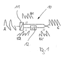
- Figure 1 shows a schematic circuit diagram of a first device for processing a digital signal of an optical transmission system according to the invention,
- figure 2 shows a schematic circuit diagram of the first device of figure 1 and a second device, and
- figure 3 shows a schematic circuit diagram of the second device of figure 2.
- In figure 1, a
first device 10 is provided that comprises a passive opticalpolarization beam splitter 11 followed by a passiveoptical phase shifter 12 at its orthogonal output. Thephase shifter 12 shifts the phase of the signal at the orthogonal output of thepolarization beam splitter 11 by n/2. The signal at the parallel output of thepolarization beam splitter 11 remains unchanged. The output of thephase shifter 12 and the parallel output of thepolarization beam splitter 11 are then combined. - The
first device 11 may be incorporated in a receiver of an optical transmission system. - A digital signal A in a bit-to-bit polarization-interleaved format is received at the input of the
polarization beam splitter 11. The signal A comprises subsequent pulses wherein the orientation of a pulse indicates the polarization state of this pulse. The subsequent pulses of the signal A, therefore, have alternating polarizations. - After passing the
polarization beam splitter 11, a signal B1 is present at the parallel output of thepolarization beam splitter 11, and a signal B2 is present at the orthogonal output of thepolarization beam splitter 11. Again, the orientation of a pulse of the signals B1, B2 indicates the polarization state of this pulse. - All pulses of the signal B1 have the same polarization. The same is valid for the pulses of the signal B2. However, the polarization of the pulses of the signal B1 is different from the polarization of the pulses of the signal B2.
- After passing the
phase shifter 12, the signal B2 has changed into the signal B2'. All pulses of the signal B2' still have the same polarization. However, compared to the signal B2, the polarization of the pulses of the signal B2' has changed. This polarization of the signal B2' is now similar to the polarization of the signal B1. - As already described, the signal B1 at the parallel output of the
polarization beam splitter 11 and the signal B2' at the output of thephase shifter 12 are then combined. The result is a signal C that has the same polarization as the signals B1 and B2'. - As a result, the
first device 10 converts the alternated-polarized signal A into the single-polarized signal C. Thefirst device 10, therefore, provides an alternated-to-single-polarization conversion of the signal A. The resulting signal C may then be processed as a single-polarized data stream. - In figure 2, the
first device 10 is shown being followed by asecond device 20. Thesecond device 20 comprises a passiveoptical delay filter 21, in particular a Mach Zehnder filter. Thedelay filter 21 comprises a first path that does not change the received signal. A second path of thedelay filter 21 delays its received signal by one bit. The two paths are then combined into the output of thedelay filter 21. - In connection with figure 3, the
second device 20 is explained in more details. It is assumed that thesecond device 20 receives the signal C from thefirst device 10. Furthermore, it is assumed that the subsequent pulses of this signal C are affected by polarization-dependent losses (PDL). Therefore, the signal at the input of the second device is characterized as a signal C*. The polarization-dependent losses are indicated in this signal C* by the different heights of the subsequent pulses. - In the mentioned second path of the
delay filter 21 of thesecond device 20, the signal C* is delayed by one bit resulting in a signal D*. Then, the signal C* of the first path and the signal D* are combined into a signal E at the output of thesecond device 20. - A comparison shows that the signal D* still incorporates the described polarization-dependent losses. However, compared to the signal C*, the heights of the subsequent pulses of the signal D* are reversed.
- This reversed sequence of the pulses of the signal D* has the consequence that the combination of this signal D* with the signal C* leads to a compensation of the polarization-dependent losses. Therefore, the signal E at the output of the
second device 20 is not affected anymore by polarization-dependent losses. This is indicated in figure 3 by the same heights of the subsequent pulses of the signal E. - The described first and
second devices
Claims (10)
- A device for processing a digital signal (A) of an optical transmission system comprising: a polarization beam splitter (11) for receiving the signal (A), a phase shifter (12) for shifting the phase of the signal (B2) at the orthogonal output of the polarization beam splitter (11), and means for combining the signal (B1) at the parallel output of the polarization beam splitter (11) and the shifted signal (B2').
- The device of claim 1 wherein the phase shifter (12) shifts the phase of its received signal (B2) by n/2.
- The device of claim 1 further comprising a delay filter (21).
- The device of claim 3 wherein the delay filter (21) delays its received signal (C*) by one bit.
- The device of claim 1 wherein the digital signal (A) is in a bit-to-bit polarization-interleaved format.
- The device of claim 1 wherein the device is used within a receiver of the optical transmission system.
- A converter for converting an alternated-polarized signal into a single-polarized signal of an optical transmission system comprising: a polarization beam splitter (11) for receiving a digital signal (A), a phase shifter (12) for shifting the phase of the signal (B2) at the orthogonal output of the polarization beam splitter (11), and means for combining the signal (B1) at the parallel output of the polarization beam splitter (11) and the shifted signal (B2').
- A method for processing a digital signal (A) of an optical transmission system comprising the steps of: receiving the signal (A) by a polarization beam splitter (11), shifting the phase of the signal (B2) at the orthogonal output of the polarization beam splitter (11), and combining the signal (B1) at the parallel output of the polarization beam splitter (11) and the shifted signal (B2').
- The method of claim 8 comprising the step of delaying the combined signal (C*).
- The method of claim 8 wherein the method is used in connection with a digital signal according to the differential phased shift keying (DPSK) format.
Priority Applications (5)
| Application Number | Priority Date | Filing Date | Title |
|---|---|---|---|
| AT04292104T ATE364265T1 (en) | 2004-08-27 | 2004-08-27 | APPARATUS AND METHOD FOR PROCESSING A DIGITAL BIT-TO-BIT POLARIZATION INTERESTED SIGNAL IN AN OPTICAL TRANSMISSION SYSTEM |
| DE602004006864T DE602004006864T2 (en) | 2004-08-27 | 2004-08-27 | Apparatus and method for processing a digital bit-to-bit polarization interleaved signal in an optical transmission system |
| EP04292104A EP1630985B1 (en) | 2004-08-27 | 2004-08-27 | A device and a method for processing a digital signal in a bit-to-bit polarization-interleaved format of an optical transmission system |
| US11/192,355 US7409166B2 (en) | 2004-08-27 | 2005-07-29 | Device and a method for processing a digital signal in a bit-to-bit polarization-interleaved format of an optical transmission system |
| CN200510093716A CN100586045C (en) | 2004-08-27 | 2005-08-23 | Device and a method for processing a digital signal of an optical transmission system |
Applications Claiming Priority (1)
| Application Number | Priority Date | Filing Date | Title |
|---|---|---|---|
| EP04292104A EP1630985B1 (en) | 2004-08-27 | 2004-08-27 | A device and a method for processing a digital signal in a bit-to-bit polarization-interleaved format of an optical transmission system |
Publications (2)
| Publication Number | Publication Date |
|---|---|
| EP1630985A1 true EP1630985A1 (en) | 2006-03-01 |
| EP1630985B1 EP1630985B1 (en) | 2007-06-06 |
Family
ID=34931355
Family Applications (1)
| Application Number | Title | Priority Date | Filing Date |
|---|---|---|---|
| EP04292104A Not-in-force EP1630985B1 (en) | 2004-08-27 | 2004-08-27 | A device and a method for processing a digital signal in a bit-to-bit polarization-interleaved format of an optical transmission system |
Country Status (5)
| Country | Link |
|---|---|
| US (1) | US7409166B2 (en) |
| EP (1) | EP1630985B1 (en) |
| CN (1) | CN100586045C (en) |
| AT (1) | ATE364265T1 (en) |
| DE (1) | DE602004006864T2 (en) |
Families Citing this family (2)
| Publication number | Priority date | Publication date | Assignee | Title |
|---|---|---|---|---|
| US20090214224A1 (en) * | 2007-04-03 | 2009-08-27 | Celight, Inc. | Method and apparatus for coherent analog rf photonic transmission |
| US9106343B2 (en) * | 2011-07-29 | 2015-08-11 | Zte (Usa) Inc. | Method and apparatus for performing temporal polarization interleaving in an optical transmitting system |
Citations (2)
| Publication number | Priority date | Publication date | Assignee | Title |
|---|---|---|---|---|
| US5822100A (en) * | 1996-06-26 | 1998-10-13 | Mci Communications Corporation | Method and system for equalizing PMD using incremental delay switching |
| US20020118422A1 (en) * | 1997-09-19 | 2002-08-29 | Siemens Telecom Networks | Method and apparatus for compensating for polarization mode dispersion (PMD) using a Mach-Zender interferometer |
Family Cites Families (4)
| Publication number | Priority date | Publication date | Assignee | Title |
|---|---|---|---|---|
| US3752992A (en) * | 1969-05-28 | 1973-08-14 | Us Navy | Optical communication system |
| CA1308440C (en) * | 1987-03-13 | 1992-10-06 | Hideaki Tsushima | Optical receiving method utilizing polarization diversity and apparatus for carrying out the same |
| US20030090768A1 (en) * | 2001-08-01 | 2003-05-15 | Xiang Liu | Long haul optical communication system |
| US6671437B2 (en) * | 2002-05-08 | 2003-12-30 | Lambda Crossing Ltd. | Method and device for tunable frequency selective filtering of optical signals |
-
2004
- 2004-08-27 EP EP04292104A patent/EP1630985B1/en not_active Not-in-force
- 2004-08-27 AT AT04292104T patent/ATE364265T1/en not_active IP Right Cessation
- 2004-08-27 DE DE602004006864T patent/DE602004006864T2/en active Active
-
2005
- 2005-07-29 US US11/192,355 patent/US7409166B2/en active Active
- 2005-08-23 CN CN200510093716A patent/CN100586045C/en not_active Expired - Fee Related
Patent Citations (2)
| Publication number | Priority date | Publication date | Assignee | Title |
|---|---|---|---|---|
| US5822100A (en) * | 1996-06-26 | 1998-10-13 | Mci Communications Corporation | Method and system for equalizing PMD using incremental delay switching |
| US20020118422A1 (en) * | 1997-09-19 | 2002-08-29 | Siemens Telecom Networks | Method and apparatus for compensating for polarization mode dispersion (PMD) using a Mach-Zender interferometer |
Non-Patent Citations (1)
| Title |
|---|
| NAPASAB V ET AL: "POLARIZATION RECOMBINING: A NEW AUTOMATIC POLARIZATION CONTROL SCHEME FOR HETERODYNE OR HOMODYNE OPTICAL RECEIVERS", JOURNAL OF OPTICAL COMMUNICATIONS, FACHVERLAG SCHIELE & SCHON, BERLIN, DE, vol. 9, no. 9, 1 September 1988 (1988-09-01), pages 102 - 107, XP000000862, ISSN: 0173-4911 * |
Also Published As
| Publication number | Publication date |
|---|---|
| US20060045538A1 (en) | 2006-03-02 |
| US7409166B2 (en) | 2008-08-05 |
| DE602004006864T2 (en) | 2008-01-31 |
| EP1630985B1 (en) | 2007-06-06 |
| CN100586045C (en) | 2010-01-27 |
| ATE364265T1 (en) | 2007-06-15 |
| DE602004006864D1 (en) | 2007-07-19 |
| CN1747361A (en) | 2006-03-15 |
Similar Documents
| Publication | Publication Date | Title |
|---|---|---|
| US8275267B2 (en) | Method, system, and apparatus for filter implementation using hermitian conjugates | |
| KR101019850B1 (en) | System and method for receiving coherent, polarization-multiplexed optical signals | |
| US9225461B2 (en) | Method of optical data transmission using mode division multiplexing | |
| US9686020B2 (en) | Signal processing device and signal processing method | |
| JP5694605B2 (en) | Multimode communication optical receiver | |
| EP2429108A1 (en) | Coherent receiver | |
| US8707138B2 (en) | Method and arrangement for blind demultiplexing a polarisation diversity multiplex signal | |
| EP2495894A1 (en) | Optical detector for detecting optical signal beams, method to detect optical signals, and use of an optical detector to detect optical signals | |
| WO2008118411A1 (en) | Filter based dpsk receiver | |
| US8750442B2 (en) | Digital receiver and waveform compensation method | |
| JPWO2012060052A1 (en) | Coherent optical receiver, system and method | |
| US8909060B2 (en) | Optical communication system and optical communication method | |
| US20120301157A1 (en) | Chromatic dispersion compensation using sign operations and lookup tables | |
| Bai et al. | Experimental demonstration of adaptive frequency-domain equalization for mode-division multiplexed transmission | |
| US7409166B2 (en) | Device and a method for processing a digital signal in a bit-to-bit polarization-interleaved format of an optical transmission system | |
| EP3072249B1 (en) | Data serializer | |
| EP3657699B1 (en) | Adaptive equalization filter and signal processing device | |
| JP2008092123A (en) | Compensation method and compensator of primary polarization mode dispersion, and optical transmission system using the same | |
| CN101162948A (en) | Method and receiver to increase the spectral efficiency of dpsk modulation format | |
| EP1942590A1 (en) | Coherent optical receiver and method of compensating polarisation distortion effects in optical signals | |
| US7272324B2 (en) | Equalization of optical signals | |
| EP3010166A1 (en) | Apparatus, Optical Receiver, Method and Computer Program for processing a first and a second electrical signal based on a polarization multiplexed signal comprising two polarizations | |
| JP6009953B2 (en) | Optical receiver | |
| JP2008092406A (en) | Frame synchronization method and optical signal receiver | |
| RU2273961C1 (en) | Device for receiving quadruple-encoded series |
Legal Events
| Date | Code | Title | Description |
|---|---|---|---|
| PUAI | Public reference made under article 153(3) epc to a published international application that has entered the european phase |
Free format text: ORIGINAL CODE: 0009012 |
|
| 17P | Request for examination filed |
Effective date: 20050726 |
|
| AK | Designated contracting states |
Kind code of ref document: A1 Designated state(s): AT BE BG CH CY CZ DE DK EE ES FI FR GB GR HU IE IT LI LU MC NL PL PT RO SE SI SK TR |
|
| AX | Request for extension of the european patent |
Extension state: AL HR LT LV MK |
|
| AKX | Designation fees paid |
Designated state(s): AT BE BG CH CY CZ DE DK EE ES FI FR GB GR HU IE IT LI LU MC NL PL PT RO SE SI SK TR |
|
| GRAP | Despatch of communication of intention to grant a patent |
Free format text: ORIGINAL CODE: EPIDOSNIGR1 |
|
| RAP1 | Party data changed (applicant data changed or rights of an application transferred) |
Owner name: ALCATEL LUCENT |
|
| GRAS | Grant fee paid |
Free format text: ORIGINAL CODE: EPIDOSNIGR3 |
|
| GRAA | (expected) grant |
Free format text: ORIGINAL CODE: 0009210 |
|
| AK | Designated contracting states |
Kind code of ref document: B1 Designated state(s): AT BE BG CH CY CZ DE DK EE ES FI FR GB GR HU IE IT LI LU MC NL PL PT RO SE SI SK TR |
|
| PG25 | Lapsed in a contracting state [announced via postgrant information from national office to epo] |
Ref country code: CH Free format text: LAPSE BECAUSE OF FAILURE TO SUBMIT A TRANSLATION OF THE DESCRIPTION OR TO PAY THE FEE WITHIN THE PRESCRIBED TIME-LIMIT Effective date: 20070606 Ref country code: LI Free format text: LAPSE BECAUSE OF FAILURE TO SUBMIT A TRANSLATION OF THE DESCRIPTION OR TO PAY THE FEE WITHIN THE PRESCRIBED TIME-LIMIT Effective date: 20070606 Ref country code: FI Free format text: LAPSE BECAUSE OF FAILURE TO SUBMIT A TRANSLATION OF THE DESCRIPTION OR TO PAY THE FEE WITHIN THE PRESCRIBED TIME-LIMIT Effective date: 20070606 |
|
| REG | Reference to a national code |
Ref country code: GB Ref legal event code: FG4D |
|
| REG | Reference to a national code |
Ref country code: CH Ref legal event code: EP |
|
| REG | Reference to a national code |
Ref country code: IE Ref legal event code: FG4D |
|
| REF | Corresponds to: |
Ref document number: 602004006864 Country of ref document: DE Date of ref document: 20070719 Kind code of ref document: P |
|
| PG25 | Lapsed in a contracting state [announced via postgrant information from national office to epo] |
Ref country code: SE Free format text: LAPSE BECAUSE OF FAILURE TO SUBMIT A TRANSLATION OF THE DESCRIPTION OR TO PAY THE FEE WITHIN THE PRESCRIBED TIME-LIMIT Effective date: 20070906 |
|
| PG25 | Lapsed in a contracting state [announced via postgrant information from national office to epo] |
Ref country code: ES Free format text: LAPSE BECAUSE OF FAILURE TO SUBMIT A TRANSLATION OF THE DESCRIPTION OR TO PAY THE FEE WITHIN THE PRESCRIBED TIME-LIMIT Effective date: 20070917 |
|
| ET | Fr: translation filed | ||
| PG25 | Lapsed in a contracting state [announced via postgrant information from national office to epo] |
Ref country code: PL Free format text: LAPSE BECAUSE OF FAILURE TO SUBMIT A TRANSLATION OF THE DESCRIPTION OR TO PAY THE FEE WITHIN THE PRESCRIBED TIME-LIMIT Effective date: 20070606 Ref country code: AT Free format text: LAPSE BECAUSE OF FAILURE TO SUBMIT A TRANSLATION OF THE DESCRIPTION OR TO PAY THE FEE WITHIN THE PRESCRIBED TIME-LIMIT Effective date: 20070606 |
|
| NLV1 | Nl: lapsed or annulled due to failure to fulfill the requirements of art. 29p and 29m of the patents act | ||
| REG | Reference to a national code |
Ref country code: CH Ref legal event code: PL |
|
| PG25 | Lapsed in a contracting state [announced via postgrant information from national office to epo] |
Ref country code: BE Free format text: LAPSE BECAUSE OF FAILURE TO SUBMIT A TRANSLATION OF THE DESCRIPTION OR TO PAY THE FEE WITHIN THE PRESCRIBED TIME-LIMIT Effective date: 20070606 |
|
| PG25 | Lapsed in a contracting state [announced via postgrant information from national office to epo] |
Ref country code: CZ Free format text: LAPSE BECAUSE OF FAILURE TO SUBMIT A TRANSLATION OF THE DESCRIPTION OR TO PAY THE FEE WITHIN THE PRESCRIBED TIME-LIMIT Effective date: 20070606 Ref country code: PT Free format text: LAPSE BECAUSE OF FAILURE TO SUBMIT A TRANSLATION OF THE DESCRIPTION OR TO PAY THE FEE WITHIN THE PRESCRIBED TIME-LIMIT Effective date: 20071106 Ref country code: NL Free format text: LAPSE BECAUSE OF FAILURE TO SUBMIT A TRANSLATION OF THE DESCRIPTION OR TO PAY THE FEE WITHIN THE PRESCRIBED TIME-LIMIT Effective date: 20070606 Ref country code: BG Free format text: LAPSE BECAUSE OF FAILURE TO SUBMIT A TRANSLATION OF THE DESCRIPTION OR TO PAY THE FEE WITHIN THE PRESCRIBED TIME-LIMIT Effective date: 20070906 Ref country code: SI Free format text: LAPSE BECAUSE OF FAILURE TO SUBMIT A TRANSLATION OF THE DESCRIPTION OR TO PAY THE FEE WITHIN THE PRESCRIBED TIME-LIMIT Effective date: 20070606 |
|
| PG25 | Lapsed in a contracting state [announced via postgrant information from national office to epo] |
Ref country code: SK Free format text: LAPSE BECAUSE OF FAILURE TO SUBMIT A TRANSLATION OF THE DESCRIPTION OR TO PAY THE FEE WITHIN THE PRESCRIBED TIME-LIMIT Effective date: 20070606 |
|
| PLBE | No opposition filed within time limit |
Free format text: ORIGINAL CODE: 0009261 |
|
| STAA | Information on the status of an ep patent application or granted ep patent |
Free format text: STATUS: NO OPPOSITION FILED WITHIN TIME LIMIT |
|
| PG25 | Lapsed in a contracting state [announced via postgrant information from national office to epo] |
Ref country code: MC Free format text: LAPSE BECAUSE OF NON-PAYMENT OF DUE FEES Effective date: 20070831 Ref country code: IT Free format text: LAPSE BECAUSE OF FAILURE TO SUBMIT A TRANSLATION OF THE DESCRIPTION OR TO PAY THE FEE WITHIN THE PRESCRIBED TIME-LIMIT Effective date: 20070606 Ref country code: DK Free format text: LAPSE BECAUSE OF FAILURE TO SUBMIT A TRANSLATION OF THE DESCRIPTION OR TO PAY THE FEE WITHIN THE PRESCRIBED TIME-LIMIT Effective date: 20070606 Ref country code: GR Free format text: LAPSE BECAUSE OF FAILURE TO SUBMIT A TRANSLATION OF THE DESCRIPTION OR TO PAY THE FEE WITHIN THE PRESCRIBED TIME-LIMIT Effective date: 20070907 |
|
| 26N | No opposition filed |
Effective date: 20080307 |
|
| PG25 | Lapsed in a contracting state [announced via postgrant information from national office to epo] |
Ref country code: RO Free format text: LAPSE BECAUSE OF FAILURE TO SUBMIT A TRANSLATION OF THE DESCRIPTION OR TO PAY THE FEE WITHIN THE PRESCRIBED TIME-LIMIT Effective date: 20070606 |
|
| PG25 | Lapsed in a contracting state [announced via postgrant information from national office to epo] |
Ref country code: IE Free format text: LAPSE BECAUSE OF NON-PAYMENT OF DUE FEES Effective date: 20070827 |
|
| PG25 | Lapsed in a contracting state [announced via postgrant information from national office to epo] |
Ref country code: EE Free format text: LAPSE BECAUSE OF FAILURE TO SUBMIT A TRANSLATION OF THE DESCRIPTION OR TO PAY THE FEE WITHIN THE PRESCRIBED TIME-LIMIT Effective date: 20070606 |
|
| PG25 | Lapsed in a contracting state [announced via postgrant information from national office to epo] |
Ref country code: CY Free format text: LAPSE BECAUSE OF FAILURE TO SUBMIT A TRANSLATION OF THE DESCRIPTION OR TO PAY THE FEE WITHIN THE PRESCRIBED TIME-LIMIT Effective date: 20070606 |
|
| PG25 | Lapsed in a contracting state [announced via postgrant information from national office to epo] |
Ref country code: LU Free format text: LAPSE BECAUSE OF NON-PAYMENT OF DUE FEES Effective date: 20070827 |
|
| PG25 | Lapsed in a contracting state [announced via postgrant information from national office to epo] |
Ref country code: TR Free format text: LAPSE BECAUSE OF FAILURE TO SUBMIT A TRANSLATION OF THE DESCRIPTION OR TO PAY THE FEE WITHIN THE PRESCRIBED TIME-LIMIT Effective date: 20070606 Ref country code: HU Free format text: LAPSE BECAUSE OF FAILURE TO SUBMIT A TRANSLATION OF THE DESCRIPTION OR TO PAY THE FEE WITHIN THE PRESCRIBED TIME-LIMIT Effective date: 20071207 |
|
| REG | Reference to a national code |
Ref country code: FR Ref legal event code: GC Effective date: 20131018 |
|
| REG | Reference to a national code |
Ref country code: FR Ref legal event code: CA Effective date: 20150521 |
|
| REG | Reference to a national code |
Ref country code: FR Ref legal event code: CA Effective date: 20150521 |
|
| REG | Reference to a national code |
Ref country code: FR Ref legal event code: PLFP Year of fee payment: 12 |
|
| REG | Reference to a national code |
Ref country code: FR Ref legal event code: PLFP Year of fee payment: 13 |
|
| REG | Reference to a national code |
Ref country code: FR Ref legal event code: PLFP Year of fee payment: 14 |
|
| PGFP | Annual fee paid to national office [announced via postgrant information from national office to epo] |
Ref country code: LU Payment date: 20180824 Year of fee payment: 11 |
|
| REG | Reference to a national code |
Ref country code: GB Ref legal event code: 732E Free format text: REGISTERED BETWEEN 20190429 AND 20190502 |
|
| REG | Reference to a national code |
Ref country code: DE Ref legal event code: R082 Ref document number: 602004006864 Country of ref document: DE Representative=s name: MENZIETTI WETZEL, DE Ref country code: DE Ref legal event code: R081 Ref document number: 602004006864 Country of ref document: DE Owner name: PROVENANCE ASSET GROUP LLC, PITTSFORD, US Free format text: FORMER OWNER: ALCATEL LUCENT, PARIS, FR |
|
| PG25 | Lapsed in a contracting state [announced via postgrant information from national office to epo] |
Ref country code: FR Free format text: LAPSE BECAUSE OF NON-PAYMENT OF DUE FEES Effective date: 20180831 |
|
| PGFP | Annual fee paid to national office [announced via postgrant information from national office to epo] |
Ref country code: DE Payment date: 20200901 Year of fee payment: 17 |
|
| PGFP | Annual fee paid to national office [announced via postgrant information from national office to epo] |
Ref country code: GB Payment date: 20201029 Year of fee payment: 17 |
|
| REG | Reference to a national code |
Ref country code: DE Ref legal event code: R119 Ref document number: 602004006864 Country of ref document: DE |
|
| GBPC | Gb: european patent ceased through non-payment of renewal fee |
Effective date: 20210827 |
|
| PG25 | Lapsed in a contracting state [announced via postgrant information from national office to epo] |
Ref country code: GB Free format text: LAPSE BECAUSE OF NON-PAYMENT OF DUE FEES Effective date: 20210827 Ref country code: DE Free format text: LAPSE BECAUSE OF NON-PAYMENT OF DUE FEES Effective date: 20220301 |