EP1630882A1 - Nanometric structure and corresponding manufacturing method - Google Patents
Nanometric structure and corresponding manufacturing method Download PDFInfo
- Publication number
- EP1630882A1 EP1630882A1 EP04425649A EP04425649A EP1630882A1 EP 1630882 A1 EP1630882 A1 EP 1630882A1 EP 04425649 A EP04425649 A EP 04425649A EP 04425649 A EP04425649 A EP 04425649A EP 1630882 A1 EP1630882 A1 EP 1630882A1
- Authority
- EP
- European Patent Office
- Prior art keywords
- spacers
- hosting
- conductive
- insulating
- nanometric
- Prior art date
- Legal status (The legal status is an assumption and is not a legal conclusion. Google has not performed a legal analysis and makes no representation as to the accuracy of the status listed.)
- Granted
Links
- 238000004519 manufacturing process Methods 0.000 title description 6
- 125000006850 spacer group Chemical group 0.000 claims abstract description 120
- 238000000034 method Methods 0.000 claims abstract description 62
- 239000000758 substrate Substances 0.000 claims abstract description 39
- 238000000151 deposition Methods 0.000 claims description 40
- 230000008021 deposition Effects 0.000 claims description 38
- 238000005530 etching Methods 0.000 claims description 35
- 239000011810 insulating material Substances 0.000 claims description 34
- 239000000463 material Substances 0.000 claims description 25
- 239000004020 conductor Substances 0.000 claims description 19
- 239000004065 semiconductor Substances 0.000 description 13
- VYPSYNLAJGMNEJ-UHFFFAOYSA-N Silicium dioxide Chemical compound O=[Si]=O VYPSYNLAJGMNEJ-UHFFFAOYSA-N 0.000 description 9
- 229910052814 silicon oxide Inorganic materials 0.000 description 9
- 238000003486 chemical etching Methods 0.000 description 6
- 239000000126 substance Substances 0.000 description 4
- 238000005516 engineering process Methods 0.000 description 3
- 238000001459 lithography Methods 0.000 description 3
- 229910021420 polycrystalline silicon Inorganic materials 0.000 description 3
- 229920005591 polysilicon Polymers 0.000 description 3
- 238000010586 diagram Methods 0.000 description 2
- 239000003989 dielectric material Substances 0.000 description 2
- 150000004767 nitrides Chemical class 0.000 description 2
- BHELIUBJHYAEDK-OAIUPTLZSA-N Aspoxicillin Chemical compound C1([C@H](C(=O)N[C@@H]2C(N3[C@H](C(C)(C)S[C@@H]32)C(O)=O)=O)NC(=O)[C@H](N)CC(=O)NC)=CC=C(O)C=C1 BHELIUBJHYAEDK-OAIUPTLZSA-N 0.000 description 1
- 229910052581 Si3N4 Inorganic materials 0.000 description 1
- XUIMIQQOPSSXEZ-UHFFFAOYSA-N Silicon Chemical compound [Si] XUIMIQQOPSSXEZ-UHFFFAOYSA-N 0.000 description 1
- 238000003491 array Methods 0.000 description 1
- 230000015572 biosynthetic process Effects 0.000 description 1
- 238000004364 calculation method Methods 0.000 description 1
- 238000007796 conventional method Methods 0.000 description 1
- 238000001900 extreme ultraviolet lithography Methods 0.000 description 1
- 230000005669 field effect Effects 0.000 description 1
- 125000000524 functional group Chemical group 0.000 description 1
- 230000010354 integration Effects 0.000 description 1
- 238000004377 microelectronic Methods 0.000 description 1
- 230000003647 oxidation Effects 0.000 description 1
- 238000007254 oxidation reaction Methods 0.000 description 1
- 238000000059 patterning Methods 0.000 description 1
- 238000001020 plasma etching Methods 0.000 description 1
- 229910052710 silicon Inorganic materials 0.000 description 1
- 239000010703 silicon Substances 0.000 description 1
- HQVNEWCFYHHQES-UHFFFAOYSA-N silicon nitride Chemical compound N12[Si]34N5[Si]62N3[Si]51N64 HQVNEWCFYHHQES-UHFFFAOYSA-N 0.000 description 1
- 238000004544 sputter deposition Methods 0.000 description 1
- 238000012876 topography Methods 0.000 description 1
- 238000001039 wet etching Methods 0.000 description 1
Images




Classifications
-
- H—ELECTRICITY
- H10—SEMICONDUCTOR DEVICES; ELECTRIC SOLID-STATE DEVICES NOT OTHERWISE PROVIDED FOR
- H10K—ORGANIC ELECTRIC SOLID-STATE DEVICES
- H10K71/00—Manufacture or treatment specially adapted for the organic devices covered by this subclass
- H10K71/60—Forming conductive regions or layers, e.g. electrodes
-
- H—ELECTRICITY
- H10—SEMICONDUCTOR DEVICES; ELECTRIC SOLID-STATE DEVICES NOT OTHERWISE PROVIDED FOR
- H10K—ORGANIC ELECTRIC SOLID-STATE DEVICES
- H10K10/00—Organic devices specially adapted for rectifying, amplifying, oscillating or switching; Organic capacitors or resistors having potential barriers
- H10K10/701—Organic molecular electronic devices
-
- Y—GENERAL TAGGING OF NEW TECHNOLOGICAL DEVELOPMENTS; GENERAL TAGGING OF CROSS-SECTIONAL TECHNOLOGIES SPANNING OVER SEVERAL SECTIONS OF THE IPC; TECHNICAL SUBJECTS COVERED BY FORMER USPC CROSS-REFERENCE ART COLLECTIONS [XRACs] AND DIGESTS
- Y10—TECHNICAL SUBJECTS COVERED BY FORMER USPC
- Y10S—TECHNICAL SUBJECTS COVERED BY FORMER USPC CROSS-REFERENCE ART COLLECTIONS [XRACs] AND DIGESTS
- Y10S977/00—Nanotechnology
- Y10S977/70—Nanostructure
- Y10S977/701—Integrated with dissimilar structures on a common substrate
- Y10S977/712—Integrated with dissimilar structures on a common substrate formed from plural layers of nanosized material, e.g. stacked structures
-
- Y—GENERAL TAGGING OF NEW TECHNOLOGICAL DEVELOPMENTS; GENERAL TAGGING OF CROSS-SECTIONAL TECHNOLOGIES SPANNING OVER SEVERAL SECTIONS OF THE IPC; TECHNICAL SUBJECTS COVERED BY FORMER USPC CROSS-REFERENCE ART COLLECTIONS [XRACs] AND DIGESTS
- Y10—TECHNICAL SUBJECTS COVERED BY FORMER USPC
- Y10S—TECHNICAL SUBJECTS COVERED BY FORMER USPC CROSS-REFERENCE ART COLLECTIONS [XRACs] AND DIGESTS
- Y10S977/00—Nanotechnology
- Y10S977/70—Nanostructure
- Y10S977/778—Nanostructure within specified host or matrix material, e.g. nanocomposite films
- Y10S977/781—Possessing nonosized surface openings that extend partially into or completely through the host material
Definitions
- the invention relates to a nanometric architecture or structure with parallel arrays as it will be better apparent in the following description.
- a nanometric electronic device as defined by the characterising part of the herewith annexed claim 11 is also claimed.
- the first array level 20 comprises insulating spacers 12 realised with a first insulating material, for example silicon oxide, whereas the second array level comprises insulating spacers 12 realised with a second insulating material, for example nitride oxide.
- the hosting structure 10 comprises conductive spacers 11 realised with polysilicon, with constant nanometric thickness "d" adjusted on the dimensions of the molecular component to be hosted, preferably below 50nm and most preferably below 10nm.
- hosting seats are defined 130a common to three array levels, and therefore common to the first array level 20, to the second array level 30 realised above the first level 20, and to the intermediate array level 40 comprised between this first 20 and second 30 array level.
- Still another advantage of the hosting structure according to the invention stays in the possibility of orienting the functionalised molecules having a different number of functionalisations, by varying the number of array levels.
- the repetition of the above steps provides the alternated deposition of layers of two different materials, conductive and insulating, in an inverted order with respect to what has been done in the depositions carried out for the realisation of the first multilayer body 70.
- these layers, conductive and insulating are deposited in the same materials used in the realisation of the first multilayer body 70, in the example polysilicon and silicon oxide, and they are again deposited with such a thickness as to allow the spacers of conductive material of overlapped multilayer bodies to lie on different and parallel planes.
- the method according to the invention thus comprises a selective etching step towards the first insulating material, with definition of a plurality of transversal slots extended along a direction perpendicular to the substrate 1, which realise a plurality of nanometric hosting seats 130b, and subsequent realisation of the above nanometric hosting structure 100b as shown in the example of figure 18.
- selective etching of a layer means any step suitable for removing such a layer, for example by means of anisotrpic chemical etching, by means of ionic bombardment or through sputtering.
- a nanometric semiconductor electronic device of the hybrid type i.e. a semiconductor device whose molecular components realised by means of suitably functionalised molecules are hosted in the hosting seats of the structure, and here suitably addressed and driven by means of conduction terminals of the structure itself.
Landscapes
- Engineering & Computer Science (AREA)
- Manufacturing & Machinery (AREA)
- Semiconductor Memories (AREA)
- Thin Film Transistor (AREA)
- Non-Volatile Memory (AREA)
- Internal Circuitry In Semiconductor Integrated Circuit Devices (AREA)
Abstract
Description
- The present invention relates, in its more general aspect, to the field of the electronics with nanometric components and to the field of the nano-manufacturing.
- In particular, the invention relates to a nanometric architecture or structure with parallel arrays as it will be better apparent in the following description.
- The word array here stands for a multispacer structure comprising a plurality of elements or spacers, being substantially bar-like, arranged according to an ordered, lined up configuration.
- The invention also relates to a realisation method of a structure of the above considered type.
- As it is well known, in the field of the microelectronics the need of realising circuit configurations of more and more reduced dimensions is particularly felt.
- In the last thirty years, the progress of the electronic technology has followed a trend governed by that which is known as "Moore Law", an empirical law stating that the capacity of storing information in memory devices doubles each eighteen months approximately, whereas the calculation performance of the CPUs (Central Processing Units) improve of a factor each twenty-four months, as reported in the diagram of figure 1.
- The Moore law is based on the capacity of reducing the geometries of the considered devices and it highlights how dimensions have passed from being equal to 2 µm for the eighties technologies, to being equal to 130 nm in 2001, to currently being equal to 90 nm.
- However, the current technology is quickly reaching the physical limits of its possibilities; in particular, the used photolitography processes are subject to drastic dimensional limitations for values being lower than 100 nm.
- Forward techniques have thus been developed such as x-ray non optic lithography or extreme ultra-violet lithography and as the electronic lithography which allow to realise circuit configurations with dimensions in the order of some tens of nanometres.
- These techniques, however, require complex instruments characterised by excessively long times of lithographic etching and they thus result too expensive for being applied to a mass industrial manufacturing.
- As an alternative, controlled deposition and selective removal techniques of a functional material on a suitable substrate have been developed.
- These techniques have allowed the adjustment of methods for realising semiconductor substrates suitable for obtaining different typologies of transistors, as for example indicated in the US patents no. 6,570,220 and no. 6 063 688 both to Doyle et el..
- In particular, in these patents a transistor with field effect is described comprising a sub-micrometric conductive region and, respectively, a relative method for realising it.
- The transistor described in such patent has a channel region comprising a plurality of conductive elements, or spacers, lined up, having a length substantially equivalent to that of the channel region, and also comprising a dielectric material to fill in the space comprised between consecutive spacers.
- The plurality of lined up conductive elements is realised by means of a method which essentially comprises the steps of realising, on a silicon substrate by means of lithography, first spacers of a first material whereon, by means of controlled deposition, a layer of a second material is then realised.
- The layer of second material is deposited with a thickness approximately corresponding to the half of the width of the first spacers.
- A selective removal step of the second material follows, carried out by means of anisotropic etching, through which second spacers each being adjacent to respective side portions of the first spacers, and each having width equal to the thickness of the layer of the second material.
- With a subsequent selective chemical etching the first spacers are removed, leaving on the surface of the semiconductor substrate the second spacers. A further step comprising the deposition of a layer of a third material, controlled in the thickness, followed by a selective removal with anisotropic etching, defined third spacers.
- These third spacers, each adjacent to respective side portions of the second spacers, have equal width to the thickness of the layer of the third material. By means of a selective chemical etching the second spacers are removed leaving on the surface of the semiconductor substrate the sole third spacers.
- The steps of controlled deposition, of anisotropic chemical etching and of selective etching are repeated more times, for realising spacers of reduced width up to 100 Å separated from one another by a distance of about 200 Å.
- By finally depositing some dielectric material in the region defined between two consecutive spacers, a conductive region is realised which can be used for realising a CMOS transistor.
- The above method needs, however, a preliminary and accurate programming since each realisation step of an order n (with n≥2) of spacers is followed by a removal step of the spacers of order (n-1), and it is thus initially necessary to provide a suitable distance and a suitable thickness of the first spacers for realising in the end last spacers of desired dimensions.
- In the US patent N° 6,664,173 to Doyle et al., a technique is also described for patterning a hardmask gate, for all the typologies of transistors, by using a gate spacer for approaching nanometric masks. This technique provides starting from a unit comprising a substrate whereon first gate and respectively hardmask layers and subsequent second gate and respectively hardmask layers are deposited.
- On the second hardmask layer, by means of deposition and thus etching steps, a nanometric spacer is defined used as mask for realising a gate electrode for a first transistor.
- From the first hardmask layer of the same unit a structure is realised for a second transistor further to other deposition and etching steps.
- Subsequent steps are however required for realising a MOS device.
- Although satisfying the aim, this method is limited in that it allows to realise, although of nanometric dimensions, a single gate electrode for a transistor.
- In substance, all the known methods clash with the need of realising nanometric structures and provided with suitable conduction and control terminals for using them as semiconductor electronic devices.
- The technical problem underlying the present invention is that of providing a method for realising a hosting structure of nanometric elements overcoming the dimensional limits of the semiconductor electronic devices realised according to the methods provided by the prior art.
- The solution idea underlying the present invention is that of providing a structure suitable for realising conduction terminals for at least one nanometric component realised by means of a molecular component, i.e. by means of a functionalised molecule capable of performing specific actions.
- On the basis of the solution idea the technical problem is solved by a nanometric semiconductor structure able to host the above molecular components, and able to realise conduction terminals for these molecular components as defined in the herewith annexed
claim 1. - The problem is also solved by a method for realising a nanometric structure as defined in the herewith annexed
claim 13. - In substance according to the invention a structure is provided able to host the above molecular components realising a semiconductor electronic device of the hybrid type.
- A nanometric electronic device as defined by the characterising part of the herewith annexed
claim 11 is also claimed. - Further characteristics and advantages of the hosting structure according to the invention will be apparent from the following description of an embodiment thereof given by way of indicative and non limiting example with reference to the annexed drawings.
-
- figure 1 is a diagram reporting the Moore Law;
- figure 2 shows a schematic, perspective, enlarged view of a nanometric structure according to the present invention;
- figure 3 shows a schematic, perspective, enlarged view of a further embodiment of the structure according to the present invention;
- figures 4 to 14 show in sequence the steps of a realisation method of the nanometric structure according to the invention;
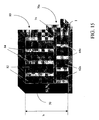
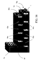
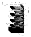
- figures 15 to 19 show some steps of the realisation method of the nanometric structure according to two alternative embodiments of the invention.
- The present invention starts from the idea of providing an electronic device comprising a plurality of molecular components as nanometric elements as well as a single hosting structure able to host such plurality of molecular components and to realise the conduction and control terminals.
- With reference to figure 2, such a hosting structure is shown, globally indicated with 10, for hosting a plurality of molecular components, not shown in the figures, according to the present invention.
- It is to be noted that the figures representing schematic views of portions of an integrated circuit during the manufacturing are not drawn to scale, but they are instead drawn so as to stress the important characteristics of the invention.
- The
hosting structure 10, realised above aninsulating substrate 1, for example a silicon oxide substrate, comprises afirst array level 20 and asecond array level 30, arranged one above the other. - Each
array level conductive spacers 11, essentially bar-like shaped, parallel to each other and having a predetermined thickness indicated with d. - These
conductive spacers 11, arranged according to a predetermined spaced relation, are perpendicular to thesubstrate 1 with definition, in eacharray level gaps 13. - Each
array level insulating spacers 12 alternated to the aboveconductive spacers 11. Theseinsulating spacers 12 are bar-like and perpendicular to thesubstrate 1. - Conveniently, in each
array level insulating spacer 12 of said plurality of insulating spacers is alternated and adjacent to a respectiveconductive spacer 11 of said plurality of conductive spacers with definition between consecutiveconductive spacers 11 of asingle gap 13. - In particular, in the example of figure 2, in correspondence with the
array 20 thegaps 13 are defined between aconductive spacer 11 and a consecutiveinsulating spacer 12, and, in correspondence with thearray 20 thegaps 13 are defined between aninsulating spacer 12 and a consecutiveconductive spacer 11. - According to the invention,
conductive spacers 11 ofconsecutive array levels substrate 1. - According to another characteristic of the invention, the above pluralities of
gaps 13 ofdifferent array levels hosting structure 10, aligned with each other, so as to define a plurality of elongated slots, here identified astransversal hosting seats 13a, extended along a direction substantially perpendicular to thesubstrate 1. - In other words, in the
hosting structure 10 eachhosting seat 13a is common to botharray levels - These
gaps 13 have a width, indicated with "I", in correspondence with thefirst array level 20, and a width indicated with "1'" in correspondence with thesecond array level 30. In a preferred embodiment of the invention, thewidths 1 and 1' are equal to each other to definehosting seats 13a having a nanometric width adjusted on the dimensions of the molecular component to be hosted, preferably below 50nm and most preferably below 10nm. - Moreover, according to another characteristic of the invention, the
hosting structure 10 comprises, interposed between the above first 20 and second 30 array level, a discontinuousinsulating layer 14 of a predetermined thickness "s", advantageously a silicon oxide layer. This discontinuous insulatinglayer 14, in practice, separates pairs of adjacent insulating 12 and conductive 11 spacers belonging to twodifferent array levels - In this way, advantageously according to the invention, the hosting
structure 10 comprises a plurality of hostingseats 13a, each hostingseat 13a being defined byside walls 15 and by a portion of thesubstrate 1 as bottom. - In particular, the
side walls 15 comprise theconductive spacers 11, as conductive portions, arranged in such a way that in a same hostingseat 13a conductive spacers of overlappedarray levels opposite side walls 15. - Preferably, the
first array level 20 comprises insulatingspacers 12 realised with a first insulating material, for example silicon oxide, whereas the second array level comprises insulatingspacers 12 realised with a second insulating material, for example nitride oxide. - Conveniently, the hosting
structure 10 comprisesconductive spacers 11 realised with polysilicon, with constant nanometric thickness "d" adjusted on the dimensions of the molecular component to be hosted, preferably below 50nm and most preferably below 10nm. - As from what has been described, the hosting
structure 10 according to the invention comprises a plurality of nanometric hostingseats 13a, having walls comprising the insulatingspacers 12 as insulating portions and theconductive spacers 11 as conductive portions. In these hostingseats 13a it is thus possible to host a plurality of functionalised nanometric molecules, or molecular components, which can be driven by conduction terminals advantageously made of the aboveconductive spacers 11 for orienting the functionalised molecules which realise them. - In the example shown in the figure, the
conductive spacers 11 arranged on two array overlappedlevels seats 13a and allow in particular to orient bi-functionalised molecules. - For hosting three-functionalised molecules, the present invention provides a hosting
structure 100, which will be described with reference to the figure 3, wherein the parts being structurally and functionally equal to those of the hostingstructure 10 preserve the same reference numbers. - The hosting
structure 100 comprises, interposed between the first 20 and the second 30 array level, anintermediate array level 40. - According to the invention, this
intermediate array level 40 comprises a plurality ofconductive spacers 41 each of them being alternated and adjacent to a relative insulatingspacer 42, with definition between consecutive pairs of adjacent conductive 41 and insulating 42 spacers of arespective gap 43. - In the hosting
structure 100, thegaps 43 of theintermediate array level 40 are aligned with thegaps 13, defined in the first 20 and in the second 30 array level, so as to define a plurality of elongated slots or transversal hostingseats 130a, extended along a direction substantially perpendicular to thesubstrate 1. - In practice, in the hosting
structure 100 hosting seats are defined 130a common to three array levels, and therefore common to thefirst array level 20, to thesecond array level 30 realised above thefirst level 20, and to theintermediate array level 40 comprised between this first 20 and second 30 array level. - Still more it can be noted that the hosting
structure 100 comprises a plurality of hostingseats 130a defined by a portion ofsubstrate 1 as bottom and by side walls 150 perpendicular to thesubstrate 1 and comprisingconductive spacers spacers seat 130a,conductive portions - In this way, in each hosting
seat 130a of the hostingstructure 100 threeconductive spacers - Conveniently, the insulating
spacers 42 of theintermediate array level 40, are realised with the same first insulating material with which the insulatingspacers 12 of thefirst array level 20 are realised; and still conveniently they have an equal thickness to the thickness of the above insulatingspacers 12 of thefirst array level 20. - Similarly to what has been seen in relation to the embodiment of figure 2, also the hosting
structure 100 comprises, between each pair of overlapped array levels, a discontinuousintermediate layer 14, advantageously a silicon oxide layer. - From what has been described it follows that, in the hosting
structure 100 according to the invention, it is possible to host, in the hostingseats 130a, three-functionalised molecules realising molecular components such as transistors. - It is also possible to orient these three-functionalised molecules by means of the
conductive spacers structure 100 which, advantageously, serve as conduction terminals for the molecular components realised by these three-functionalised molecules. - For hosting particularly complex molecules or molecular components, it is possible to provide in the hosting structure according to the invention, further
intermediate array levels 40 arranged on growing planes, comprised between the first and thesecond array level - It is also possible to provide, comprised between consecutive pairs of these further
intermediate array levels 40, discontinuous insulatingintermediate layers 14. - It is still possible to provide, in the hosting structure according to the invention,
conductive spacers 11 of a same array level having variable thickness; or it is possible to provide a constant thickness in each of the array level and being different from different array levels. - Also the hosting
seats - The main advantage of the hosting structure according to the present invention stays in the nanometric dimensions it has. In particular it stays in the nanometric dimensions conferred to the hosting seats and to the conductive spacers of the different array levels.
- The conductive spacers define conductive portions of the walls which delimit these hosting seats, and therefore they allow to retain and drive inside the hosting seats nanometric transistors suitably orienting the properly functionalised molecules which realise them.
- Another advantage of the here considered hosting structure, is represented by the arrangement of the conductive spacers which are faced and alternated, considering consecutive array levels and a single hosting seat, on opposite side walls of this hosting seat. A similar arrangement allows to minimise, in the molecules hosted in the hosting structure, tensions due to the steric space of the functional groups used for the functionalisation.
- Still another advantage of the hosting structure according to the invention stays in the possibility of orienting the functionalised molecules having a different number of functionalisations, by varying the number of array levels.
- Another advantage stays in the possibility of orienting functionalised molecules having variable dimensions, by varying the width of the hosting seats; as well as of varying the properties of the conduction terminals of the molecular components realised by these functionalised molecules, by varying the thickness of the conductive spacers i.e. of the conduction terminals themselves.
- A last but not less important advantage of the hosting structure according to the invention, stays in the capacity of hosting and orienting, in each of the hosting seats, more functionalised molecules or molecular components, "flanked" one to the other, allowing to realise semiconductor electronic devices having a high integration or component density.
- It is thus possible to realise a nanometric electronic device by providing a nanometric hosting structure as previously described and to host therein a plurality of nanometric components, in particular molecular components having respective conduction terminals realised by the conductive spacers of the hosting structure.
- With reference to the figures 4 to 14, an embodiment of a manufacturing method of a nanometric structure according to the present invention is now described.
- The steps hereafter described are not a complete flow of a method for realising such a structure and only those steps are described being necessary to a medium technician of the field for the comprehension of the invention.
- The here considered realisation method can be put into practice by using the common techniques employed in the manufacturing of the semiconductor electronic devices.
- The method according to the invention first provides a deposition step, on an upper surface 1a of an insulating
substrate 1, of a block-seed 50 having aside wall 50a of predetermined height indicated with "h" perpendicular to this upper surface 1a of thesubstrate 1. - The block-
seed 50 is thus defined by means of a selective chemical etching so as to ensure a good squaring of the block-seed 50 i.e. the perpendicularity relation between theside wall 50a of the block-seed 50 and the upper surface 1a of thesubstrate 1. - This of the block-
seed 50 is for example realised with a specific material, such as silicon nitride. It is also possible to realise this block-seed 50 by means of deposition of a plurality of overlapped layers also of different material. - The method thus comprises a succession of steps repeated m times and in each case at least three times, each of them including a deposition, on the insulating
substrate 1, of alayer layer spacer - In particular, as shown in the example of the figures 5 to 8 where a double repetition is shown, it can be noted how in the deposition, carried out according to conventional techniques, the deposited layer adapts conformably to the underlying topography, thus also to the block-
seed 50, whereas the anisotropic etching removes the depositedlayer substrate 1, with definition of theabove spacer substrate 1 itself. - More specifically, the method according to the invention comprises the alternated deposition of
layers - The
spacers layer side wall 50a of the block-seed 50, and which comprisesm spacers - According of the invention, the method thus comprises a dimensioning or reduction step of the
first multilayer body 70 with removal of a portion thereof and realisation of a ri-dimensionedmultilayer body 70a, or reduced multilayer body, having a lower height than the height "h" of theside wall 50a of the block-seed 50, as shown in figure 11. - Conveniently, said dimensioning step is carried out according to several strategies, for example by exploiting a partial chemical etching comprising at least a first step of first selective etching towards the first insulating material forming the
spacers 62, as shown in figure 10 where ri-dimensioned insulatingspacers 62a can be noted, having a lower height than the height "h" of theconductive spacers 64 they are alternated with. - The dimensioning step thus comprises a second selective etching step towards the conductive material forming the
spacers 64, with realisation of ri-dimensionedconductive spacers 64a, having height equal to the ri-dimensioned insulatingspacers 62a to form the ri-dimensionedmultilayer body 70a, as shown in figure 11. - According to the invention, the method thus comprises n repetitions, with n ≥ 3, of the above steps each comprising the deposition of a layer of a predetermined material and the consecutive anisotropic etching step of the deposited layer, and wherein in each tern of consecutive depositions three layers are deposited of three different materials by using again as block-seed the
block 50. - In this way, above the first ri-dimensioned
multilayer body 70a, asecond multilayer body 70b is realised comprisingn spacers substrate 1, respectively realised with conductive material and with two different insulating materials, as highlighted in figure 13. - Preferably these two different insulating materials are made of the above first insulating material, in the example silicon oxide, and of a second insulating material, for example nitride oxide.
- According to a characteristic of the invention, in each of the above steps the depositions of each layer are controlled in the thickness so as to realise, further to each relative subsequent anisotropic etching,
spacers second multilayer body 70b, lie on different planes. - The method according to the invention thus comprises a selective etching step, generally a plasma etching, through which defined portions of
spacers multilayer body 70a and in thesecond multilayer body 70b,. - In particular, a selective etching step is provided towards the first insulating material, with removal of the
spacers second multilayer body 70b (which thus does not have insulating material of the first residual type) and partial in the first ri-dimensionedmultilayer body 70a, by not removing in this latter portions of the above ri-dimensionedspacers 62a, masked by, i.e. underlying the spacers of second insulatingmaterial 72 and ofconductive material 71 of thesecond multilayer body 70b. In substance, at the end of this etching step, a hosting structure is realised, similar to the hostingstructure 10 previously described with reference to figure 2 and having afirst array level 20 comprising insulatingspacers 12 realised with the first insulating material, alternated and adjacent toconductive spacers 11, as well as asecond array 30, overlapped to thefirst array 20 and comprising insulating spacers, alternated and adjacent toconductive spacers 11. - The hosting
structure 10 realised with the above described method has, inside thesecond array 30, insulating spacers realised with the second insulating material and indicated with 12b, corresponding to the insulatingspacers 12 as previously described with reference to figure 2. - Advantageously in the method according to the invention, the last selective etching step towards the first insulating material allows to define a plurality of transversal slots extended along a direction perpendicular to the
substrate 1, with realisation of a plurality of hostingseats 13a for thenanometric hosting structure 10, shown in figure 14. - The method further provides a removal step of the block-
seed 50, not shown in the figures, carried out by means of a conventional selective etching, for example through steam isotropic technique (Isotropic Wet Etching). - Preferably, the method according to the invention also comprises a deposition step of an intermediate insulating
layer 74, above a multilayer body and prior to the formation of a multilayer body overlapped thereto. In particular, in figure 12 this intermediate insulatinglayer 74 is shown being deposited above the first ri-dimensionedmultilayer body 70a. - Advantageously, this intermediate insulating
layer 74 is realised with the same insulating material used in the deposition steps for realising themultilayer bodies structure 10 according to the invention, of a discontinuous insulatinglayer 14 interposed between the first and thesecond array level - Alternatively, this deposition step of an intermediate insulating
layer 74 can comprise the deposition of an intermediate insulating layer of a different material. In this case, the method will comprise a selective etching step towards the material of the an intermediate insulatinglayer 74. - The important thing is that, according to the invention, a last selective etching step is provided, wherein portions are removed both from the first ri-dimensioned
multilayer body 70a and from thesecond multilayer body 70b, so as to realise the above transversal slots defining the desired hostingseats 13a. - The dimensions of the spacers and the insulating layers are nanometric, preferably below 50nm and most preferably below 10nm; they are adjusted on the dimensions and on the type of electric behaviour which is performed by the molecular components to be hosted.
- It is obviously possible to deposit, in the realisation of a same array level or of different array levels, layers of a same material having non uniform thickness for realising spacers, conductive or insulating, and nanometric hosting seats, of variable dimensions.
- In a further embodiment of the method according to the invention, shown with reference to figures 15 to 18, a hosting
structure 100b is realised suitable for hosting more complex functionalised molecules, for example three-functionalised. - In particular, according to this embodiment, the method further provides the realisation of an intermediate ri-dimensioned
multilayer body 80a, interposed between the above ri-dimensionedmultilayer body 70a and the abovesecond multilayer body 70b. - First of all, above the first ri-dimensioned
multilayer body 70a anintermediate multilayer body 80 is realised by means of the repetition of the above m steps, comprising each the deposition of a layer of predetermined material followed by an anisotropic etching of the deposited layer with realisation for each repetition of a relative layer element orspacer - Subsequently, a dimensioning step is provided of the
intermediate multilayer body 80 with removal of a portion thereof and realisation of the above intermediate ri-dimensionedmultilayer body 80a having a lower height than the height "h" of the side wall of the block-seed 50, as shown in figure 16. - Preferably, the repetition of the above steps provides the alternated deposition of layers of two different materials, conductive and insulating, in an inverted order with respect to what has been done in the depositions carried out for the realisation of the
first multilayer body 70. - Conveniently these layers, conductive and insulating, are deposited in the same materials used in the realisation of the
first multilayer body 70, in the example polysilicon and silicon oxide, and they are again deposited with such a thickness as to allow the spacers of conductive material of overlapped multilayer bodies to lie on different and parallel planes. - Preferably, the deposition of these layers is carried out after the above deposition step of the intermediate insulating
layer 74, whereas the dimensioning step of the intermediate insulatinglayer 80 is preferably followed by a further deposition step of a further intermediate insulatinglayer 74. - Advantageously, the intermediate insulating
layers 74 are deposited in the same first insulating material, in the example silicon oxide. - In practice, as highlighted in the example of figure 17, three multilayer bodies are realised on three different levels. The first ri-dimensioned
multilayer body 70a and the intermediate ri-dimensionedmultilayer body 80a there above, comprise each, being alternated one another, spacers realised withconductive material second multilayer body 70b, realised in turn above the intermediate ri-dimensionedmultilayer body 80a, also comprisesspacers 72 realised with a second insulating material, as previously shown. - The method according to the invention thus comprises a selective etching step towards the first insulating material, with definition of a plurality of transversal slots extended along a direction perpendicular to the
substrate 1, which realise a plurality of nanometric hostingseats 130b, and subsequent realisation of the abovenanometric hosting structure 100b as shown in the example of figure 18. - It is to be noted how it is possible and preferred, through the control of the thickness of the deposited layers, with subsequent control of the width of the spacers realised therefrom in each of the multilayer bodies, to realise, further to the last selective etching step, a hosting
structure 100 as the one represented in figure 19, wherein in eachtransversal slot 130a three conductive spacers are faced 11, as previously described in relation to the figure 3. This hostingstructure 100 is particularly advantageous since all the hostingseats 130a can be exploited for hosting, addressing and driving molecular components such as transistors, by orienting the three-functionalised molecules which realise them. - Obviously, the last selective etching step will be liable to comprise more differently selective etching operations, in the case wherein the intermediate insulating layers, such as the insulating spacers in the different multilayer bodies, are realised with more different insulating layers.
- It is naturally possible, with the method according to the invention, to realise nanometric hosting structures comprising more than three array levels, for hosting even more complex funxtionalised molecules.
- In practice, hosting structures of this type can be realised by repeating the steps which lead to the realisation of further ri-dimensioned intermediate multilayer bodies, eventually separated by further intermediate insulating layers.
- It is important, in the repetition of these steps, to control the thickness of the deposited layers so as to realise conductive spacers, i.e. conductive terminals, lying, considering consecutive array levels, on different and parallel planes.
- Obviously, in the present description and in the following claims, deposition of a layer of insulating material, in particular if an insulating oxide is considered, stands for any step suitable for realising such a layer; thus both a step comprising an effective deposition of the insulating oxide for example by means of "CVD-oxide" technique (control vapor oxide), and a step comprising a growth of the oxide from an underlying layer, for example with a "thermal oxidation" technique.
- Similarly, selective etching of a layer means any step suitable for removing such a layer, for example by means of anisotrpic chemical etching, by means of ionic bombardment or through sputtering.
- The main advantage of the method according to the present invention stays in the possibility of realising a nanometric structure, in particular a structure comprising nanometric hosting seats suitable for hosting, addressing and driving nanometric molecular components realised by means of functionalised molecules.
- In particular the method according to the invention allows to realise a plurality of nanometric conduction terminals, arranged on a desired number of parallel and growing planes, which face in the above hosting seats for driving the above molecular components, by orienting the functionalised molecules which realise them.
- A further advantage of the present method stays in the possibility of realising a structure of the above considered type, wherein both the plurality of hosting seats and the conduction terminals can be realised with different dimensions.
- This realisation allows to host molecular components of different nature and dimensions, and of individually asking the single terminals.
- A further advantage of the method according to the invention stays in its easiness and speed of realisation steps being provided which are easy to be integrated in the productive processes currently in use for realising semiconductor devices.
- In substance, thanks to the present invention it is possible to realise a nanometric semiconductor electronic device of the hybrid type, i.e. a semiconductor device whose molecular components realised by means of suitably functionalised molecules are hosted in the hosting seats of the structure, and here suitably addressed and driven by means of conduction terminals of the structure itself.
- In particular, it is possible to predispose the hosting structure for hosting the molecular components as described in the European patent application No. 1 278 234 filed on 23/11/2001 to the same Applicant. By using the method described in this application, the molecular components in the hosting seats of the structure automatically bond to the conductive spacers which realise the conduction terminals.
- Advantageously, the realisation of the hosting structure is completed prior to the hosting therein of the molecular components and to the subsequent realisation of the desired hybrid semiconductor device. In this way, the molecular components do not undergo any stress linked to the process steps for realising the hosting structure.
- Obviously, a technician of the field will bring, with the aim of meeting contingent and specific needs, several changes to the above described invention all however within the scope of protection of the invention, as defined by the hereafter reported claims.
Claims (26)
- Hosting structure of nanometric components characterised in that it comprises- a substrate (1);- n array levels (20, 30, 40) on said substrate (1), with n ≥ 2, arranged consecutively on growing and parallel planes,
each including a plurality of conductive spacers (11, 41) alternated to a plurality of insulating spacers (12, 42) and substantially perpendicular to said substrate (1), with definition between consecutive conductive spacers (11, 41) of at least a gap (13),
conductive spacers of consecutive array levels (20, 30, 40) lying on distinct and parallel planes, said gaps (13) of different array levels being at least partially aligned along a direction substantially perpendicular to said substrate (1) with definition of a plurality of transversal hosting seats (13a, 130a) extended along said direction and suitable for hosting at least a nanometric component. - Structure according to claim 1, characterised in that the conductive spacers (11, 41) of overlapped array levels (20-30, 20-40, 40-30) face in a same hosting seat (13a, 130a) opposite side walls (15) of said hosting seat (13a, 130a), said side walls (15) being substantially perpendicular to said substrate (1).
- Structure according to claim 2, characterised in that said conductive spacers (11, 41) realise conduction terminals for molecular components hosted in said plurality of hosting seats (13a, 130a).
- Structure according to claim 1, characterised in that it comprises between each pair of consecutive array levels a discontinuous insulating layer (14).
- Structure according to claim 1, characterised in that a single gap is defined between consecutive pairs of said adjacent spacers respectively conductive (11) and insulating (12).
- Structure according to any of the preceding claims, characterised in that an array level includes insulating spacers (12, 12b) realised in at least two different insulating materials.
- Structure according to any of the preceding claims, characterised in that conductive spacers (11) of a same array level have constant thickness.
- Structure according to any of the preceding claims, characterised in that conductive spacers (11) of different array levels have equal thickness to each other.
- Structure according to any of the preceding claims, characterised in that gaps (13) of different array levels have equal widths to each other.
- Structure according to any of the preceding claims, characterised in that said hosting seats (13a, 130a) have a predetermined constant width.
- Nanometric electronic device characterised in that it comprises at least a nanometric component hosted in a hosting structure (10, 100) according to any of the preceding claims, said conductive spacers (11, 41) of said hosting structure defining respective conduction terminals of said at least one nanometric component.
- Electronic device according to claim 11, characterised in that said at least one nanometric component comprises a molecular component realised by a functionalised molecule.
- Method for realising a hosting structure of nanometric components comprising:A) a deposition step, on an upper surface (1a) of a substrate (1), of a block-seed (50) having at least a side wall (50a) substantially perpendicular to said upper surface (1a);B) a first repetition of m steps, with m > 3, each step comprising:a deposition on said substrate (1) of a layer (52, 54) of a predetermined material, and an anisotropic etching of said layer (52, 54), with realisation, at each repetition, of at least one relative spacer (62, 64) substantially perpendicular to said upper surface (1a),said predetermined material being different for each pair of consecutive depositions, said m steps defining at least a first multilayer body (70) comprising m spacers (62, 64) realised with at least two different materials alternated to each other, respectively a first insulating material and a conductive material,C) a dimensioning step with removal of a portion of said at least one multilayer body (70) and realisation of at least one ri-dimensioned multilayer body (70a) having a lower height than said block-seed (50);D) a second repetition of n steps, with n ≥ 3, each of said steps comprising a deposition of a layer and an anisotropic etching of the deposited layer, by depositing at least three different materials in each tern of consecutive deposition realising, above said at least a first ri-dimensioned multilayer body (70a), at least a second multilayer body (70b) comprising n spacers (71, 72, 73) realised with at least three different materials respectively with a conductive material and with at least two different insulating materials;E) at least a selective etching step of multilayer body for removing in said multilayer bodies (70a, 70b) defined portions of said spacers (62a, 73) of insulating material with definition of a plurality of nanometric, transversal hosting seats (13a, 130a), extended along a direction substantially perpendicular to said substrate (1).
- Method according to claim 13, characterised in that said depositions of layers of conductive material are controlled in the thickness realising, further to each relative anisotropic etching, spacers (11) of conductive material lying in said multilayer bodies (70a, 70b), on different planes perpendicular to said substrate (1).
- Method according to claim 13, characterised in that it further comprises a selective removal step of said block-seed (50).
- Method according to claim 15, characterised in that said selective removal step of said block-seed (50) is carried out after said second repetition of n steps.
- Method according to claim 15, characterised in that said selective removal step of said block-seed (50) is carried out after said at least one selective etching step of multilayer body.
- Method according to any claim 13 to 17, characterised in that it comprises at least a further first repetition of m steps with realisation of at least one intermediate multilayer body (80) and at least a further dimensioning step of said at least one intermediate multilayer body (80) with realisation of at least an intermediate ri-dimensioned multilayer body (80a) comprised between said at least a first ri-dimensioned multilayer body (70a) and said at least a second multilayer body (70b).
- Method according to claim 18, characterised in that said depositions of layer of conductive material of said further first repetition of m steps is controlled in the thickness realising, further to each relative anisotropic etching, spacers of conductive material (84) lying in consecutive multilayer bodies (70a-80a, 80a-70b), on different planes perpendicular to said substrate (1).
- Method according to any claim 13 to 19, further comprising subsequently to at least one of said dimensioning steps a deposition step of an intermediate insulating layer (74) of predetermined thickness.
- Method according to any claim 13 to 20, wherein said dimensioning step comprises a first selective partial etching towards one among said conductive or insulating material, and a second selective partial etching towards the other among said conductive or insulating materials.
- Method according to claim 20, wherein said intermediate insulating layer (74) is realised with said first insulating material.
- Method according to claim 13, wherein one of said different insulating materials is equal to said first insulating material.
- Method according to any claim 13 to 23, characterised in that said depositions of conductive material deposit layers of equal thickness to each other, with realisation of said conductive spacers (11, 41) having equal widths to each other.
- Method according to any claim 13 to 23, characterised in that said depositions of conductive material deposit layers of different thickness to each other, with realisation of said conductive spacers (11, 41) having different widths to each other.
- Method according to any claim 13 to 25, characterised in that said depositions of conductive material deposit said layers with thickness adjusted according to the nanometric dimensions and to the type of electric behaviour which said molecular component to be hosted performs, preferably below 50nm and most preferably below 10nm.
Priority Applications (3)
| Application Number | Priority Date | Filing Date | Title |
|---|---|---|---|
| EP04425649A EP1630882B1 (en) | 2004-08-31 | 2004-08-31 | Nanometric structure and corresponding manufacturing method |
| US11/215,296 US7834344B2 (en) | 2004-08-31 | 2005-08-30 | Nanometric structure and corresponding manufacturing method |
| CN2005100966751A CN1755938B (en) | 2004-08-31 | 2005-08-31 | Nanostructures and corresponding manufacturing methods |
Applications Claiming Priority (1)
| Application Number | Priority Date | Filing Date | Title |
|---|---|---|---|
| EP04425649A EP1630882B1 (en) | 2004-08-31 | 2004-08-31 | Nanometric structure and corresponding manufacturing method |
Publications (2)
| Publication Number | Publication Date |
|---|---|
| EP1630882A1 true EP1630882A1 (en) | 2006-03-01 |
| EP1630882B1 EP1630882B1 (en) | 2012-05-02 |
Family
ID=34932737
Family Applications (1)
| Application Number | Title | Priority Date | Filing Date |
|---|---|---|---|
| EP04425649A Expired - Lifetime EP1630882B1 (en) | 2004-08-31 | 2004-08-31 | Nanometric structure and corresponding manufacturing method |
Country Status (3)
| Country | Link |
|---|---|
| US (1) | US7834344B2 (en) |
| EP (1) | EP1630882B1 (en) |
| CN (1) | CN1755938B (en) |
Families Citing this family (26)
| Publication number | Priority date | Publication date | Assignee | Title |
|---|---|---|---|---|
| US8362559B2 (en) * | 2002-02-01 | 2013-01-29 | William Marsh Rice University | Hybrid molecular electronic devices containing molecule-functionalized surfaces for switching, memory, and sensor applications and methods for fabricating same |
| EP1630882B1 (en) | 2004-08-31 | 2012-05-02 | STMicroelectronics S.r.l. | Nanometric structure and corresponding manufacturing method |
| EP1630127B1 (en) * | 2004-08-31 | 2008-09-10 | STMicroelectronics S.r.l. | Method for realising a hosting structure of nanometric elements |
| EP1630881B1 (en) * | 2004-08-31 | 2011-11-16 | STMicroelectronics Srl | Hosting structure of nanometric elements and corresponding manufacturing method |
| US7492624B2 (en) * | 2007-06-29 | 2009-02-17 | Stmicroelectronics S.R.L. | Method and device for demultiplexing a crossbar non-volatile memory |
| KR20100028412A (en) * | 2008-09-04 | 2010-03-12 | 삼성전자주식회사 | Light emitting diode using nano-rod and method for manufacturing the same |
| US8563086B2 (en) | 2009-07-22 | 2013-10-22 | Korea Institute Research and Business Foundation | Nano pattern formation |
| US8592732B2 (en) * | 2009-08-27 | 2013-11-26 | Korea University Research And Business Foundation | Resistive heating device for fabrication of nanostructures |
| CN103641062B (en) * | 2013-12-17 | 2016-08-17 | 安徽华东光电技术研究所 | A kind of method preparing micro-nano structure |
| CN103762136B (en) * | 2014-01-21 | 2016-02-24 | 安徽华东光电技术研究所 | A kind of manufacture method of parallel grating |
| CN104037038B (en) * | 2014-05-13 | 2016-04-27 | 安徽华东光电技术研究所 | Method for preparing rectangular grating structure by using same material thin plate |
| CN113985017A (en) | 2016-01-14 | 2022-01-28 | 罗斯韦尔生物技术股份有限公司 | Molecular sensors and related methods |
| JP7280590B2 (en) | 2016-01-28 | 2023-05-24 | ロズウェル バイオテクノロジーズ,インコーポレイテッド | Methods and apparatus for measuring analytes using large-scale molecular electronics sensor arrays |
| EP3408219B1 (en) | 2016-01-28 | 2022-08-17 | Roswell Biotechnologies, Inc | Massively parallel dna sequencing apparatus |
| KR20240170584A (en) | 2016-02-09 | 2024-12-03 | 로스웰 엠이 아이엔씨. | Electronic label-free dna and genome sequencing |
| US10597767B2 (en) | 2016-02-22 | 2020-03-24 | Roswell Biotechnologies, Inc. | Nanoparticle fabrication |
| US9829456B1 (en) * | 2016-07-26 | 2017-11-28 | Roswell Biotechnologies, Inc. | Method of making a multi-electrode structure usable in molecular sensing devices |
| KR102622275B1 (en) | 2017-01-10 | 2024-01-05 | 로스웰 바이오테크놀로지스 인코포레이티드 | Methods and systems for DNA data storage |
| CA3052140A1 (en) | 2017-01-19 | 2018-07-26 | Roswell Biotechnologies, Inc. | Solid state sequencing devices comprising two dimensional layer materials |
| EP3615685B1 (en) | 2017-04-25 | 2025-02-19 | Roswell Biotechnologies, Inc | Enzymatic circuits for molecular sensors |
| US10508296B2 (en) | 2017-04-25 | 2019-12-17 | Roswell Biotechnologies, Inc. | Enzymatic circuits for molecular sensors |
| EP4023764A3 (en) | 2017-05-09 | 2022-09-21 | Roswell Biotechnologies, Inc. | Binding probe circuits for molecular sensors |
| CN111373049A (en) | 2017-08-30 | 2020-07-03 | 罗斯威尔生命技术公司 | Progressive enzyme molecular electronic sensor for DNA data storage |
| CN111373051A (en) | 2017-10-10 | 2020-07-03 | 罗斯威尔生命技术公司 | Methods, devices and systems for amplification-free DNA data storage |
| CN113994013A (en) | 2019-04-12 | 2022-01-28 | 罗斯威尔生命技术公司 | Polycyclic aromatic bridges for molecular electronic sensors |
| US12146852B2 (en) | 2019-09-06 | 2024-11-19 | Roswell Biotechnologies, Inc. | Methods of fabricating nanoscale structures usable in molecular sensors and other devices |
Citations (5)
| Publication number | Priority date | Publication date | Assignee | Title |
|---|---|---|---|---|
| US20020043690A1 (en) * | 1997-09-29 | 2002-04-18 | Doyle Brian S. | Fabrication of deep submicron structures and quantum wire transistors using hard-mask transistor width definition |
| WO2002035580A2 (en) * | 2000-10-24 | 2002-05-02 | Molecular Electronics Corporation | Three-terminal field-controlled molecular devices |
| WO2003005369A2 (en) * | 2001-07-05 | 2003-01-16 | Infineon Technologies Ag | Molecular electronics arrangement and method for producing a molecular electronics arrangement |
| EP1278234A2 (en) * | 2001-07-19 | 2003-01-22 | STMicroelectronics S.r.l. | MOS transistor and method of manufacturing |
| DE10247679A1 (en) | 2002-10-12 | 2004-04-22 | Fujitsu Ltd., Kawasaki | Semiconductor body structure, as a biosensor, has two thick layers of one material separated by a thin different intermediate layer forming a nano gap, with organic wire structures as the contacts |
Family Cites Families (25)
| Publication number | Priority date | Publication date | Assignee | Title |
|---|---|---|---|---|
| US5262336A (en) | 1986-03-21 | 1993-11-16 | Advanced Power Technology, Inc. | IGBT process to produce platinum lifetime control |
| US4758531A (en) | 1987-10-23 | 1988-07-19 | International Business Machines Corporation | Method of making defect free silicon islands using SEG |
| US5272114A (en) | 1990-12-10 | 1993-12-21 | Amoco Corporation | Method for cleaving a semiconductor crystal body |
| US5520244A (en) | 1992-12-16 | 1996-05-28 | Sdl, Inc. | Micropost waste heat removal system |
| JPH06334262A (en) | 1993-03-23 | 1994-12-02 | Mitsubishi Electric Corp | Semiconductor laser array device, semiconductor laser device, and manufacturing method thereof |
| IL121312A (en) | 1997-07-14 | 2001-09-13 | Technion Res & Dev Foundation | Microelectronic components, their fabrication and electronic networks comprising them |
| US6358854B1 (en) | 1999-04-21 | 2002-03-19 | Sandia Corporation | Method to fabricate layered material compositions |
| US6365059B1 (en) | 2000-04-28 | 2002-04-02 | Alexander Pechenik | Method for making a nano-stamp and for forming, with the stamp, nano-size elements on a substrate |
| GB0026471D0 (en) | 2000-10-30 | 2000-12-13 | Univ Cambridge Tech | Small-scale structures |
| DE10118197C2 (en) | 2001-04-11 | 2003-04-03 | Infineon Technologies Ag | Integrated magnetoresistive semiconductor memory device and method for describing the same |
| DE10123364C2 (en) | 2001-05-14 | 2003-04-24 | Infineon Technologies Ag | Component with molecular photodiode and integrated circuit based thereon |
| US6824974B2 (en) | 2001-06-11 | 2004-11-30 | Genorx, Inc. | Electronic detection of biological molecules using thin layers |
| JP2003100902A (en) | 2001-09-21 | 2003-04-04 | Mitsubishi Electric Corp | Method for manufacturing semiconductor device |
| FR2834130B1 (en) | 2001-12-20 | 2005-02-18 | Thales Sa | PROCESS FOR IMPROVING THE OPTICAL CHARACTERISTICS OF MULTILAYER OPTOELECTRONIC COMPONENTS |
| US6664173B2 (en) * | 2002-01-09 | 2003-12-16 | Intel Corporation | Hardmask gate patterning technique for all transistors using spacer gate approach for critical dimension control |
| JP2003309194A (en) | 2002-04-18 | 2003-10-31 | Nec Electronics Corp | Semiconductor storage device and its manufacturing method |
| US6882553B2 (en) * | 2002-08-08 | 2005-04-19 | Micron Technology Inc. | Stacked columnar resistive memory structure and its method of formation and operation |
| JP4789619B2 (en) | 2002-11-12 | 2011-10-12 | ホーヤ コーポレイション ユーエスエイ | Optical device and optical assembly incorporating optical device |
| KR100565174B1 (en) * | 2003-11-20 | 2006-03-30 | 한국전자통신연구원 | Manufacturing method of nanogap electrode device |
| US7366009B2 (en) | 2004-01-10 | 2008-04-29 | Honeywell International Inc. | Separate write and read access architecture for a magnetic tunnel junction |
| EP1630127B1 (en) * | 2004-08-31 | 2008-09-10 | STMicroelectronics S.r.l. | Method for realising a hosting structure of nanometric elements |
| EP1630882B1 (en) | 2004-08-31 | 2012-05-02 | STMicroelectronics S.r.l. | Nanometric structure and corresponding manufacturing method |
| EP1630881B1 (en) * | 2004-08-31 | 2011-11-16 | STMicroelectronics Srl | Hosting structure of nanometric elements and corresponding manufacturing method |
| US7355230B2 (en) | 2004-11-30 | 2008-04-08 | Infineon Technologies Ag | Transistor array for semiconductor memory devices and method for fabricating a vertical channel transistor array |
| KR100673012B1 (en) | 2005-09-02 | 2007-01-24 | 삼성전자주식회사 | A dynamic random access memory device having double gate type vertical channel transistors and a method of manufacturing the same |
-
2004
- 2004-08-31 EP EP04425649A patent/EP1630882B1/en not_active Expired - Lifetime
-
2005
- 2005-08-30 US US11/215,296 patent/US7834344B2/en not_active Expired - Fee Related
- 2005-08-31 CN CN2005100966751A patent/CN1755938B/en not_active Expired - Fee Related
Patent Citations (5)
| Publication number | Priority date | Publication date | Assignee | Title |
|---|---|---|---|---|
| US20020043690A1 (en) * | 1997-09-29 | 2002-04-18 | Doyle Brian S. | Fabrication of deep submicron structures and quantum wire transistors using hard-mask transistor width definition |
| WO2002035580A2 (en) * | 2000-10-24 | 2002-05-02 | Molecular Electronics Corporation | Three-terminal field-controlled molecular devices |
| WO2003005369A2 (en) * | 2001-07-05 | 2003-01-16 | Infineon Technologies Ag | Molecular electronics arrangement and method for producing a molecular electronics arrangement |
| EP1278234A2 (en) * | 2001-07-19 | 2003-01-22 | STMicroelectronics S.r.l. | MOS transistor and method of manufacturing |
| DE10247679A1 (en) | 2002-10-12 | 2004-04-22 | Fujitsu Ltd., Kawasaki | Semiconductor body structure, as a biosensor, has two thick layers of one material separated by a thin different intermediate layer forming a nano gap, with organic wire structures as the contacts |
Also Published As
| Publication number | Publication date |
|---|---|
| CN1755938A (en) | 2006-04-05 |
| US20060051919A1 (en) | 2006-03-09 |
| CN1755938B (en) | 2010-05-12 |
| EP1630882B1 (en) | 2012-05-02 |
| US7834344B2 (en) | 2010-11-16 |
Similar Documents
| Publication | Publication Date | Title |
|---|---|---|
| EP1630882B1 (en) | Nanometric structure and corresponding manufacturing method | |
| EP1630127B1 (en) | Method for realising a hosting structure of nanometric elements | |
| KR100223807B1 (en) | Manufacturing method of semiconductor device | |
| US10297659B2 (en) | Memory devices including capacitor structures having improved area efficiency | |
| US20200303644A1 (en) | Resistance variable memory device with nanoparticle electrode and method of fabrication | |
| JP6815953B2 (en) | How to Form a Semiconductor Device Structure Including a Step Step Structure | |
| Frascaroli et al. | Resistive switching in high-density nanodevices fabricated by block copolymer self-assembly | |
| US20100301449A1 (en) | Methods and apparatus for forming line and pillar structures for three dimensional memory arrays using a double subtractive process and imprint lithography | |
| US9960046B2 (en) | Methods of manufacturing semiconductor device having a blocking insulation layer | |
| TW201117270A (en) | Integrated nanostructure-based non-volatile memory fabrication | |
| CN1510740A (en) | Method for fabricating memory with nanodots | |
| EP1568087A1 (en) | Non-volatile memory cell, memory cell arrangement and method for production of a non-volatile memory cell | |
| JP2007277085A (en) | Method for positioning nanoparticles on substrate | |
| CN100401500C (en) | Method for manufacturing nanoscale MOSFET transistor and nanoscale transistor array | |
| CN115298133A (en) | Quantum dot device | |
| US7928578B2 (en) | Electric linkage in a semiconductor electronic device between a nanometric circuit architecture and standard electronic components | |
| US7456508B2 (en) | Hosting structure of nanometric elements and corresponding manufacturing method | |
| CN110299365B (en) | Semiconductor memory device | |
| JP4031619B2 (en) | Ferroelectric film, ferroelectric film manufacturing method, ferroelectric capacitor, ferroelectric capacitor manufacturing method, ferroelectric memory device, ferroelectric memory device manufacturing method | |
| Cerofolini et al. | The multi-spacer patterning technique: a non-lithographic technique for terascale integration | |
| CN113950742A (en) | Three-dimensional NAND memory device and method of forming the same | |
| JP3998916B2 (en) | Ferroelectric film, ferroelectric film manufacturing method, ferroelectric capacitor, ferroelectric capacitor manufacturing method, ferroelectric memory device, and ferroelectric memory device manufacturing method | |
| JP4221853B2 (en) | Storage device | |
| KR100543077B1 (en) | High aspect ratio electrode manufacturing method | |
| CN113659076A (en) | Method for preparing domain wall memory and domain wall memory |
Legal Events
| Date | Code | Title | Description |
|---|---|---|---|
| PUAI | Public reference made under article 153(3) epc to a published international application that has entered the european phase |
Free format text: ORIGINAL CODE: 0009012 |
|
| AK | Designated contracting states |
Kind code of ref document: A1 Designated state(s): AT BE BG CH CY CZ DE DK EE ES FI FR GB GR HU IE IT LI LU MC NL PL PT RO SE SI SK TR |
|
| AX | Request for extension of the european patent |
Extension state: AL HR LT LV MK |
|
| 17P | Request for examination filed |
Effective date: 20060830 |
|
| AKX | Designation fees paid |
Designated state(s): DE FR GB IT |
|
| 17Q | First examination report despatched |
Effective date: 20081211 |
|
| RAP1 | Party data changed (applicant data changed or rights of an application transferred) |
Owner name: STMICROELECTRONICS SRL |
|
| RIC1 | Information provided on ipc code assigned before grant |
Ipc: G11C 13/02 20060101ALI20110829BHEP Ipc: H01L 51/00 20060101AFI20110829BHEP Ipc: B82Y 10/00 20110101ALI20110829BHEP |
|
| GRAP | Despatch of communication of intention to grant a patent |
Free format text: ORIGINAL CODE: EPIDOSNIGR1 |
|
| GRAS | Grant fee paid |
Free format text: ORIGINAL CODE: EPIDOSNIGR3 |
|
| GRAA | (expected) grant |
Free format text: ORIGINAL CODE: 0009210 |
|
| AK | Designated contracting states |
Kind code of ref document: B1 Designated state(s): DE FR GB IT |
|
| RAP1 | Party data changed (applicant data changed or rights of an application transferred) |
Owner name: STMICROELECTRONICS S.R.L. |
|
| REG | Reference to a national code |
Ref country code: GB Ref legal event code: FG4D |
|
| RAP2 | Party data changed (patent owner data changed or rights of a patent transferred) |
Owner name: STMICROELECTRONICS SRL |
|
| REG | Reference to a national code |
Ref country code: DE Ref legal event code: R096 Ref document number: 602004037592 Country of ref document: DE Effective date: 20120705 |
|
| PG25 | Lapsed in a contracting state [announced via postgrant information from national office to epo] |
Ref country code: IT Free format text: LAPSE BECAUSE OF FAILURE TO SUBMIT A TRANSLATION OF THE DESCRIPTION OR TO PAY THE FEE WITHIN THE PRESCRIBED TIME-LIMIT Effective date: 20120502 |
|
| PLBE | No opposition filed within time limit |
Free format text: ORIGINAL CODE: 0009261 |
|
| STAA | Information on the status of an ep patent application or granted ep patent |
Free format text: STATUS: NO OPPOSITION FILED WITHIN TIME LIMIT |
|
| 26N | No opposition filed |
Effective date: 20130205 |
|
| GBPC | Gb: european patent ceased through non-payment of renewal fee |
Effective date: 20120831 |
|
| REG | Reference to a national code |
Ref country code: FR Ref legal event code: ST Effective date: 20130430 |
|
| REG | Reference to a national code |
Ref country code: DE Ref legal event code: R097 Ref document number: 602004037592 Country of ref document: DE Effective date: 20130205 |
|
| PG25 | Lapsed in a contracting state [announced via postgrant information from national office to epo] |
Ref country code: GB Free format text: LAPSE BECAUSE OF NON-PAYMENT OF DUE FEES Effective date: 20120831 |
|
| PG25 | Lapsed in a contracting state [announced via postgrant information from national office to epo] |
Ref country code: FR Free format text: LAPSE BECAUSE OF NON-PAYMENT OF DUE FEES Effective date: 20120831 |
|
| PGFP | Annual fee paid to national office [announced via postgrant information from national office to epo] |
Ref country code: DE Payment date: 20130722 Year of fee payment: 10 |
|
| REG | Reference to a national code |
Ref country code: DE Ref legal event code: R119 Ref document number: 602004037592 Country of ref document: DE |
|
| REG | Reference to a national code |
Ref country code: DE Ref legal event code: R119 Ref document number: 602004037592 Country of ref document: DE Effective date: 20150303 |
|
| PG25 | Lapsed in a contracting state [announced via postgrant information from national office to epo] |
Ref country code: DE Free format text: LAPSE BECAUSE OF NON-PAYMENT OF DUE FEES Effective date: 20150303 |