EP1625679B1 - High speed, silicon-based electro-optic modulator - Google Patents
High speed, silicon-based electro-optic modulator Download PDFInfo
- Publication number
- EP1625679B1 EP1625679B1 EP04751784A EP04751784A EP1625679B1 EP 1625679 B1 EP1625679 B1 EP 1625679B1 EP 04751784 A EP04751784 A EP 04751784A EP 04751784 A EP04751784 A EP 04751784A EP 1625679 B1 EP1625679 B1 EP 1625679B1
- Authority
- EP
- European Patent Office
- Prior art keywords
- arrangement
- emphasis
- optical
- modulator
- signal
- Prior art date
- Legal status (The legal status is an assumption and is not a legal conclusion. Google has not performed a legal analysis and makes no representation as to the accuracy of the status listed.)
- Active
Links
Images


Classifications
-
- G—PHYSICS
- G02—OPTICS
- G02F—OPTICAL DEVICES OR ARRANGEMENTS FOR THE CONTROL OF LIGHT BY MODIFICATION OF THE OPTICAL PROPERTIES OF THE MEDIA OF THE ELEMENTS INVOLVED THEREIN; NON-LINEAR OPTICS; FREQUENCY-CHANGING OF LIGHT; OPTICAL LOGIC ELEMENTS; OPTICAL ANALOGUE/DIGITAL CONVERTERS
- G02F1/00—Devices or arrangements for the control of the intensity, colour, phase, polarisation or direction of light arriving from an independent light source, e.g. switching, gating or modulating; Non-linear optics
- G02F1/01—Devices or arrangements for the control of the intensity, colour, phase, polarisation or direction of light arriving from an independent light source, e.g. switching, gating or modulating; Non-linear optics for the control of the intensity, phase, polarisation or colour
- G02F1/21—Devices or arrangements for the control of the intensity, colour, phase, polarisation or direction of light arriving from an independent light source, e.g. switching, gating or modulating; Non-linear optics for the control of the intensity, phase, polarisation or colour by interference
- G02F1/225—Devices or arrangements for the control of the intensity, colour, phase, polarisation or direction of light arriving from an independent light source, e.g. switching, gating or modulating; Non-linear optics for the control of the intensity, phase, polarisation or colour by interference in an optical waveguide structure
-
- G—PHYSICS
- G02—OPTICS
- G02F—OPTICAL DEVICES OR ARRANGEMENTS FOR THE CONTROL OF LIGHT BY MODIFICATION OF THE OPTICAL PROPERTIES OF THE MEDIA OF THE ELEMENTS INVOLVED THEREIN; NON-LINEAR OPTICS; FREQUENCY-CHANGING OF LIGHT; OPTICAL LOGIC ELEMENTS; OPTICAL ANALOGUE/DIGITAL CONVERTERS
- G02F1/00—Devices or arrangements for the control of the intensity, colour, phase, polarisation or direction of light arriving from an independent light source, e.g. switching, gating or modulating; Non-linear optics
- G02F1/01—Devices or arrangements for the control of the intensity, colour, phase, polarisation or direction of light arriving from an independent light source, e.g. switching, gating or modulating; Non-linear optics for the control of the intensity, phase, polarisation or colour
- G02F1/015—Devices or arrangements for the control of the intensity, colour, phase, polarisation or direction of light arriving from an independent light source, e.g. switching, gating or modulating; Non-linear optics for the control of the intensity, phase, polarisation or colour based on semiconductor elements with at least one potential jump barrier, e.g. PN, PIN junction
- G02F1/025—Devices or arrangements for the control of the intensity, colour, phase, polarisation or direction of light arriving from an independent light source, e.g. switching, gating or modulating; Non-linear optics for the control of the intensity, phase, polarisation or colour based on semiconductor elements with at least one potential jump barrier, e.g. PN, PIN junction in an optical waveguide structure
-
- G—PHYSICS
- G02—OPTICS
- G02F—OPTICAL DEVICES OR ARRANGEMENTS FOR THE CONTROL OF LIGHT BY MODIFICATION OF THE OPTICAL PROPERTIES OF THE MEDIA OF THE ELEMENTS INVOLVED THEREIN; NON-LINEAR OPTICS; FREQUENCY-CHANGING OF LIGHT; OPTICAL LOGIC ELEMENTS; OPTICAL ANALOGUE/DIGITAL CONVERTERS
- G02F1/00—Devices or arrangements for the control of the intensity, colour, phase, polarisation or direction of light arriving from an independent light source, e.g. switching, gating or modulating; Non-linear optics
- G02F1/01—Devices or arrangements for the control of the intensity, colour, phase, polarisation or direction of light arriving from an independent light source, e.g. switching, gating or modulating; Non-linear optics for the control of the intensity, phase, polarisation or colour
- G02F1/011—Devices or arrangements for the control of the intensity, colour, phase, polarisation or direction of light arriving from an independent light source, e.g. switching, gating or modulating; Non-linear optics for the control of the intensity, phase, polarisation or colour in optical waveguides, not otherwise provided for in this subclass
-
- G—PHYSICS
- G02—OPTICS
- G02F—OPTICAL DEVICES OR ARRANGEMENTS FOR THE CONTROL OF LIGHT BY MODIFICATION OF THE OPTICAL PROPERTIES OF THE MEDIA OF THE ELEMENTS INVOLVED THEREIN; NON-LINEAR OPTICS; FREQUENCY-CHANGING OF LIGHT; OPTICAL LOGIC ELEMENTS; OPTICAL ANALOGUE/DIGITAL CONVERTERS
- G02F1/00—Devices or arrangements for the control of the intensity, colour, phase, polarisation or direction of light arriving from an independent light source, e.g. switching, gating or modulating; Non-linear optics
- G02F1/01—Devices or arrangements for the control of the intensity, colour, phase, polarisation or direction of light arriving from an independent light source, e.g. switching, gating or modulating; Non-linear optics for the control of the intensity, phase, polarisation or colour
- G02F1/0121—Operation of devices; Circuit arrangements, not otherwise provided for in this subclass
-
- H—ELECTRICITY
- H04—ELECTRIC COMMUNICATION TECHNIQUE
- H04B—TRANSMISSION
- H04B10/00—Transmission systems employing electromagnetic waves other than radio-waves, e.g. infrared, visible or ultraviolet light, or employing corpuscular radiation, e.g. quantum communication
- H04B10/50—Transmitters
- H04B10/501—Structural aspects
- H04B10/503—Laser transmitters
- H04B10/505—Laser transmitters using external modulation
-
- H—ELECTRICITY
- H04—ELECTRIC COMMUNICATION TECHNIQUE
- H04B—TRANSMISSION
- H04B10/00—Transmission systems employing electromagnetic waves other than radio-waves, e.g. infrared, visible or ultraviolet light, or employing corpuscular radiation, e.g. quantum communication
- H04B10/50—Transmitters
- H04B10/58—Compensation for non-linear transmitter output
-
- G—PHYSICS
- G02—OPTICS
- G02B—OPTICAL ELEMENTS, SYSTEMS OR APPARATUS
- G02B6/00—Light guides; Structural details of arrangements comprising light guides and other optical elements, e.g. couplings
- G02B6/10—Light guides; Structural details of arrangements comprising light guides and other optical elements, e.g. couplings of the optical waveguide type
- G02B6/12—Light guides; Structural details of arrangements comprising light guides and other optical elements, e.g. couplings of the optical waveguide type of the integrated circuit kind
- G02B2006/12133—Functions
- G02B2006/12145—Switch
-
- G—PHYSICS
- G02—OPTICS
- G02F—OPTICAL DEVICES OR ARRANGEMENTS FOR THE CONTROL OF LIGHT BY MODIFICATION OF THE OPTICAL PROPERTIES OF THE MEDIA OF THE ELEMENTS INVOLVED THEREIN; NON-LINEAR OPTICS; FREQUENCY-CHANGING OF LIGHT; OPTICAL LOGIC ELEMENTS; OPTICAL ANALOGUE/DIGITAL CONVERTERS
- G02F1/00—Devices or arrangements for the control of the intensity, colour, phase, polarisation or direction of light arriving from an independent light source, e.g. switching, gating or modulating; Non-linear optics
- G02F1/01—Devices or arrangements for the control of the intensity, colour, phase, polarisation or direction of light arriving from an independent light source, e.g. switching, gating or modulating; Non-linear optics for the control of the intensity, phase, polarisation or colour
- G02F1/015—Devices or arrangements for the control of the intensity, colour, phase, polarisation or direction of light arriving from an independent light source, e.g. switching, gating or modulating; Non-linear optics for the control of the intensity, phase, polarisation or colour based on semiconductor elements with at least one potential jump barrier, e.g. PN, PIN junction
- G02F1/0151—Devices or arrangements for the control of the intensity, colour, phase, polarisation or direction of light arriving from an independent light source, e.g. switching, gating or modulating; Non-linear optics for the control of the intensity, phase, polarisation or colour based on semiconductor elements with at least one potential jump barrier, e.g. PN, PIN junction modulating the refractive index
- G02F1/0152—Devices or arrangements for the control of the intensity, colour, phase, polarisation or direction of light arriving from an independent light source, e.g. switching, gating or modulating; Non-linear optics for the control of the intensity, phase, polarisation or colour based on semiconductor elements with at least one potential jump barrier, e.g. PN, PIN junction modulating the refractive index using free carrier effects, e.g. plasma effect
Definitions
- the present invention relates to silicon-based electro-optic modulators and, more particularly, to the provision of high speed (e.g., greater than 1 Gb/s) modulators by incorporating channel equalization techniques into the modulator and associated electronic drive circuit.
- high speed modulators e.g., greater than 1 Gb/s
- Optical transmission systems are generally based on one of two methods of modulation of an optical signal, either direct modulation or external modulation.
- the bias current applied to a laser is modulated, turning the laser "on” and “off".
- the disadvantage of this method is that when higher switching speeds are required, the dynamic behavior of the semiconductor material of the laser itself introduces distortion, primarily in the form of chirp.
- External modulation of an optical signal with a modulating electrical signal produces a modulated optical output signal with significantly reduced chirp, and external modulators have become preferred for high speed applications.
- electro-optic modulators such as Mach Zehnder interferometers are typically used for high speed applications.
- Optical waveguides are formed within the electro-optic material, with metal contact regions disposed on the surface of each waveguide arm.
- the application of a voltage to a metal contact will modify the refractive index of the waveguide region underneath the contact, thus changing the speed of propagation along the waveguide.
- a nonlinear (digital) Mach-Zehnder modulator is formed.
- the optical signal is launched into the waveguide, and the 1/0 electrical digital signal input is applied to the contacts (using proper voltage levels, as mentioned above).
- the optical output is then "modulated" to create an optical 1/0 output signal.
- a similar result is possible with a linear (analog) optical output signal.
- FIG. 1 illustrates one exemplary arrangement of a silicon-based modulator device as disclosed in our co-pending application.
- a "MOSCAP" structure 1 in terms of a doped (i.e., "metal-like") silicon layer 2 (usually polysilicon) is disposed over a doped portion of a relatively thin (sub-micron) surface layer 3 of a silicon-on-insulator (SOI) wafer 4, this thin surface layer 3 often being referred to in the art as the "SOI layer".
- SOI silicon-on-insulator
- a thin dielectric layer 5 is located between the doped, "metal"-like" polysilicon layer 2 and the doped SOI layer 3, with the layers disposed so that an overlap is formed, as shown in FIG. 1 , to define an active region of the device.
- Free carriers will accumulate and deplete on either side of dielectric layer 5 as a function of voltages applied to SOI layer 3 (VREF3) and/or polysilicon layer 2 (VREF2).
- the modulation of the free carrier concentration results in changing the effective refractive index in the active region, thus introducing phase modulation of an optical signal propagating along a waveguide formed along the active region (the waveguide being in the direction perpendicular to the paper).
- optical loss is controlled by reducing optical signal absorption along the extent of the waveguide. Since the absorption is directly related to the carrier doping density, a minimal optical loss requires a minimal dopant density in both polysilicon layer 2 and SOI layer 3.
- this optical loss specification runs in direct opposition to the desire for high speed operation. That is, to provide a high speed (i.e., switching speed greater than I Gb/s) device, a relatively high doping density is required. Inasmuch as system requirements are even now moving toward 10 Gb/s, there is a strong need to increase the switching speed of a silicon-based electro-optic modulator, without sacrificing optical power to attain high speed operation.
- US Patent Application Publication 2003/0058504 describes an optical modulator utilizing a phase shift keyed (PSK) modulation technique and further embedding a plurality of adjacent return-to-zero optical pulses within the data stream to overcome problems associated with dispersion along an optical fiber transmission path.
- Adjacent return-to-zero pulses preferably have an extinction ratio therebetween of about 15dB (or at least 20dB).
- US Patent Application Publication 2002/0018280 describes an optical modulator that includes a diode mounted on a high-frequency circuit substrate to "shape" the electrical data signal input applied to the modulator so as to improve the output optical waveguide when the extinction characteristic of the input light source is nonlinear.
- an arrangement for generating a high speed optical output signal modulated by an input data pattern as defined in claim 1.
- the present invention relates to silicon-based electro-optic modulators and, more particularly, to the provision of high speed (e.g., greater than 1 Gb/s) modulators by incorporating channel equalization techniques into the modulator and associated electronic drive circuit.
- channel equalization is achieved by developing a doping profile for the device terminals that provides the desired limit of optical loss. For a given doping profile, there will be an associated maximum switching speed at which the modulator will function when using a simple drive circuit (i.e., a transition between two reference voltage levels, such as VDD and VSS, to switch between an optical"0"and an optical"1").
- a simple drive circuit i.e., a transition between two reference voltage levels, such as VDD and VSS, to switch between an optical"0"and an optical"1".
- pre-emphasis voltages are applied during transitions between" 1 "and"0" (falling edge transitions), as well as between"0"and “1” (rising edge transitions), where the pre-emphasis voltage will accelerate charging and discharging of the MOSCAP (or modulator active capacitance), thus reducing the fall and rise times respectively between states.
- MOSCAP modulator active capacitance
- the pre-emphasis circuits and techniques described hereinbelow also allow for an impedance transformation from the data source (usually a 50 Q impedance) to a much lower value (certainly less than 25 Q and usually about I Q), thus approaching an ideal voltage source.
- the optimum pre-emphasis voltage levels and pulse durations may be defined during manufacture, on a device- by-device basis, and stored in a microprocessor-related memory (or other memory type device) co-located with the modulator.
- a feedback technique may use a table of reference voltages and associated pre-emphasis voltage/duration values (stored in the look-up table), where as modulation conditions change (i.e., temperature, supply voltage variations, lifetime aging etc.), the optimum parameter values may be selected from the database to adjust the device performance.
- the use of pre-emphasis to extend the channel bandwidth reduces the pattern dependent jitter by increasing the bandwidth of the channel.
- a portion of the optical output signal may be tapped off and analyzed to determine the necessary changes.
- a preferred layout arrangement of the present invention utilizes a plurality of separate contact points along the length of the polysilicon layer and the SOI layer in the contact region. Since the speed of light is finite in silicon, the "flight time" of the optical signal along the length of the modulator may become a significant portion of the bit period. Thus, by fanning out (i.e., distributing) the electrical signal input along the extent of the active region, the entire waveguide is essentially energized simultaneously such that all parts of the waveguide instantaneously see the change in voltage.
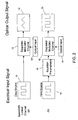
- FIG. 2 illustrates, in simplified form, a nonlinear channel equalization arrangement showing the use of an equalizer/pre-emphasis circuit of the present invention to improve the optical output characteristics of a high speed optical modulator.
- FIG. 2(a) illustrates a bandwidth limited channel arrangement, where an electrical input data signal from a data source 10 is applied as the electrical input to a silicon-based modulator structure 12, such as the modulator illustrated in FIG. 1 .
- a silicon-based modulator structure 12 such as the modulator illustrated in FIG. 1 .
- electro-optic modulators include, but are not limited to, free carrier-based modulators, particularly silicon-based electro-optic modulates.
- an optical input from a light source 14 is applied as the second input to modulator 12, where as discussed in our above-cited co-pending application, the optical signal is coupled into the relatively thin SOI layer (such as SOI layer 3 of FIG. 1 ) and thereafter propagates along the active region of the waveguide structure.
- the switching speed of the electrical input signal from source 10 goes above a certain value (for example, above 1 Gb/s)
- the free carriers in the silicon-based modulator cannot charge or discharge the modulator fast enough to completely change state during the bit period.
- the modulator performance begins to degrade, and the optical output signal becomes distorted, as shown by element 16 in FIG. 2(a) .
- FIG. 2(b) illustrates, in simplified form, the solution as proposed by the present invention, where an equalizer/pre-emphasis circuit 18 is disposed between the electrical input source 10 and modulator structure 12.
- Equalizer/pre-emphasis circuit 18 is configured to recognize each transition between the logic levels in the input signal, and insert an additional "boost" to the voltage applied at the transition.
- This pre-emphasis voltage pulse functions to accelerate the free carrier movement, so that essentially all of charging or discharging has completed by the end of the bit period. Therefore, the optical output signal, as shown by element 20, remains clean, with sharp, clearly-defined transitions between optical "1" and optical "0".
- Equalizer/pre-emphasis circuit 18 thus allows for the bandwidth of modulator structure 12 to be extended without increasing the optical loss of the system. Indeed, the doping profile within the active region can remain at a relatively low level (for example, 1X10 19 cm 3 ) and still provide optical switching greater than 1 Gb/s.
- FIG. 3 illustrates a simplified linear channel equalization arrangement in block diagram form, the contrast between a distortion limited channel arrangements ( FIG. 3(a) ) and an arrangement utilizing an equalizer/pre-emphasis circuit in accordance with the present invention ( FIG. 3(b) ) to linearize the modulator channel.
- modulator 12 and optical source 14 are the same as those associated with FIG. 2 .
- a linear electrical signal source 22 is illustrated as being applied as the electrical input to modulator 12.
- pre-emphasis circuit 26 functions to boost the extremes of the linear input voltage signal (i.e., pre-emphasis), thus increasing the linear range of the modulator.
- the resultant output, as shown in element 28, thus more closely tracks the shape (and frequency) of the input.
- pre-emphasis as a linear channel equalization technique provides an improvement in the optical output power, as illustrated in FIG.
- 3(c) which contains plots of the optical output power as a function of the electrical input power, the dashed curve associated with the arrangement without pre-emphasis. As shown, there is a gradual, asymptotic curve toward the maximum power for this arrangement. In contrast, the arrangement of the present invention including pre-emphasis allows for a constant increase in optical output power increasing the linear dynamic range, reaching the maximum value without gain compression avoiding signal distortion. Ultimately at some power level, clipping occurs causing distortion but linearized devices are not operated at or above the saturation point. In fact, significant linear range is achieved using pre-emphasis well before reaching the saturation point. The saturation point can only be increased by increases in the operating supply voltage.
- FIG. 4 illustrates a simplified block diagram for an exemplary Mach Zehnder interferometer modulator showing the individual accumulation and depletion arms of the design.
- Each arm of the interferometer contains a phase modulator device with two terminals.
- Terminal 1 is made from a silicon (often polysilicon) layer 2 as described in FIG. 1 , doped n-type as region 50 in the accumulation arm and 60 for the depletion arm.
- Terminal 2 is formed in the SOI layer 3 also shown in FIG. 1 , doped p-type as region 56 in the accumulation arm and 62 for the depletion arm.
- FIG. 5 contains a set of reference voltages and drive patterns associated with the bandwidth-limited channel arrangement of FIG. 2(a) and distortion-limited channel arrangement of FIG. 3(a) .
- the exemplary optical data to be transmitted is illustrated along the top trace A in FIG. 5 .
- One arrangement for providing this data pattern as an input to modulator 12 is for the output from electrical data source 10 to hold one terminal at a pre-defmed reference potential (in this case "terminal 2" is held at VDD), shown as trace B.
- the remaining terminal (“terminal 1") is then moved about a second reference potential (REF1A/REF1D) to define optical "1" and "0", as shown in trace C.
- REF1A/REF1D second reference potential
- the state of optical "1" is defined when terminal 1 of both the accumulation and depletion arms of a modulator of FIG. 4 are held at this pre-defined reference voltage (i.e., REF1A ⁇ REF1D).
- REF0D higher voltage
- REF0A lower voltage
- VSS low as VSS
- FIG. 6 contains an exemplary set of reference voltages and drive patterns including pre-emphasis that can be used to accomplish increased switching speed (greater than 1 Gb/s) in accordance with the present invention. As with the prior art set of drive patterns shown in FIG.
- terminal 2 in the pre-emphasis case can be held at a predetermined reference potential (e.g., VDD), and the voltage applied to "terminal 1" changed as a function of the data pattern to impose this data pattern on the propagating optical signal.
- a predetermined reference potential e.g., VDD
- the state of optical "1" is defined for the inventive arrangement when terminal 1 of both the accumulation and depletion arms of a modulator of FIG. 4 are held at essentially the same pre-defined reference voltage (i.e., REF1A ⁇ REF1D).
- the voltage applied to terminal 1 of the depletion arm includes an initial pulse that will over-shoot the voltage level associated with the steady-state value of optical "0" (REF0D), the initial pulse having a magnitude M D10 and time duration T D10 sufficient to accelerate the movement of free carriers out of the depletion arm device channel.
- This shaded pulse region is illustrated as “D10” in FIG. 6 , where the same pulse D10 will be applied to the depletion arm for every transition from optical "1" to optical "0".
- the voltage applied to terminal 1 of the accumulation arm includes an initial pulse that over-shoots the voltage level associated with the steady-state value of optical "0" (REF0A), where the pulse magnitude M A10 and time duration t A10 are chosen to accelerate the accumulation of free carriers in the accumulation arm device channel.
- This shaded pulse region is illustrated as “A10” in FIG. 6 , wherein the same pulse A10 will be applied to the accumulation arm for every (falling edge) transition from optical "1" to optical "0".
- pre-emphasis may also be used during the transition from optical "0" to optical "1", to again enhance the movement of free carriers and enable higher switching speeds.
- an over-shoot pulse denoted D01 is added to the voltage change needed to switch the accumulation arm from REF0D to REF1D, where pulse D01 is illustrated as comprising a predetermined magnitude M D01 and time duration t D01 .
- the pre-emphasis associated with the accumulation arm is illustrated as pulse A01, having a magnitude of M A01 and time duration t A01 .
- each of the various pulse magnitudes and time durations for the "1" to "0" transition and “0" to “1” transition for both the accumulation and depletion arms may be different, since the movement of free carriers in each state may be different and may require pulses of higher/lower magnitude, and for a longer/shorter time duration. It is an aspect of the present invention to individually tailor each one of these variables for each case, thus optimizing the movement of free carriers and enabling high speed operation for the optical modulator. Moreover, there may be instances where only "rising edge” pre-emphasis is desired, or perhaps only “falling edge” pre-emphasis. All of these cases are considered to fall within the scope of the present invention.
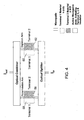
- FIG. 7 is a top view, in simplified form, of an exemplary Mach-Zehnder electro-optic modulator 30 formed in accordance with the present invention to provide for high speed (greater than 1 Gb/s) operation.
- An optical signal I in is illustrated as traveling along an input waveguide 32 and entering an optical splitter 34.
- input waveguide 32 and optical splitter 34 may be formed within the SOI layer of an SOI wafer (such as SOI layer 3 of FIG. 1 ).
- Optical splitter 34 may simply divide the optical power present in the signal in half, such that a balanced 50/50 split of signal I in is presented to each arm of modulator 30.
- any other split may be used, or even desired, depending on the parameters of the accumulation and depletion arms (parameters such as doping concentration, length of each active area, materials used to form terminal 1 and terminal 2, etc.).
- a first output from optical splitter 34 denoted as I inA is thereafter applied as the optical input signal to accumulation arm 36, where optical signal I inA propagates along an optical waveguide 38 formed along the extent of accumulation arm 36.
- a second output from optical splitter 34, denoted as I inD is thereafter applied as the optical input signal to depletion arm 40, where optical signal I inD propagates along an optical waveguide 42 formed along the extent of depletion arm 40.
- the active waveguiding areas where modulation occurs are formed by overlapping portions of the SOI layer (such as SOI layer 3 of FIG. 1 ) and an overlying silicon layer (for example, polysilicon layer 2 of FIG. 1 ), with a relatively thin dielectric layer (layer 5) disposed therebetween.
- the dielectric layer is not evident in the top view of modulator 30 of FIG. 7 , but is visible in the device side view of FIG. 1 .
- the "terminal 1" material, illustrated as region 50 comprises a portion of silicon (usually polysilicon) layer 2 of FIG.
- terminal 1 that has been doped (for example, "n" doped), where the doping profile may be preferably controlled in accordance with the present invention to form a lightly doped portion within active waveguide area 52, and a more heavily doped portion along the terminal 1 electrical contact area 54.
- the "terminal 2" material which may comprise SOI layer 3 of FIG. 1 , is formed as shown under doped region 50 of terminal 1.
- Terminal 2 SOI region 56 (which is oppositely doped with respect to the terminal 1 region) is formed to overlap region 50 in active waveguide area 52, then extend in the opposite direction to form its contact area 58. As before, the doping density of region 56 is maintained at a lower level in active waveguide area 52 to minimize optical loss (while allowing for a heavier doping density in contact area 58).
- Polysilicon regions 50 and 60 include input and output tapered regions to present a graded index change to an optical signal entering and exiting active waveguide areas 52 and 64, thus minimizing optical reflections at the inputs and outputs of the associated active waveguide areas.
- polysilicon region 50 is illustrated as including an input taper 66 and an output taper 68
- polysilicon region 60 is illustrated as including an input taper 70 and an output taper 72.
- the input tapers 66 and 70 function to gradually increase the effective refractive index of the waveguide layer, where the gradual tapers will introduce less reflection than simply disposing a polysilicon layer over the SOI layer and introducing an abrupt change in refractive index to a propagating optical signal.
- output tapers 68 and 72 will gradually decrease the effective refractive index.
- a detailed description of the use of such tapered polysilicon layers may be found in our co-pending application Serial No. 10/818,415, filed April 5, 2004 .
- SOI regions 56 and 62 being defined as the "terminal 2" inputs for accumulation arm 36 and depletion arm 40, respectively, are coupled, in this particular example, to a reference voltage (such as VDD in this embodiment).
- a set of four different input signals are shown as coupled (in this embodiment) to the "terminal 1" connections for accumulation arm 36 and depletion arm 40. These signals correspond to those discussed above in association with FIG.
- a pre-emphasis pulse for an optical "0" to “1” transition a reference level for optical "1", a reference level for optical "0”, and a pre-emphasis pulse for an optical "1" to “0” transition.
- these various inputs are controlled to apply the proper pre-emphasis signals at each transition, followed by the proper reference level for the remainder of the duration of the particular logic level.
- FIG. 8 is a preferred embodiment of modulator 30 of FIG. 7 , in terms of the voltage levels used to define the reference voltages and the pre-emphasis voltages.
- FIG. 9 is a diagram of the reference voltages and drive patterns associated with the arrangement of FIG. 8 .
- terminal 2 is fixed at a reference voltage potential of VDD (the conventional drain voltage for CMOS applications).
- VDD the conventional drain voltage for CMOS applications.
- the maximum voltage level for applying a pre-emphasis pulse to terminal 1 of accumulation arm 36 for an optical "0" to "1” transition is also defined as VDD.
- the VDD voltage level is used to define the maximum level of a pre-emphasis pulse for a "1" to "0” transition on depletion arm 40.
- VDD the conventional drain voltage for CMOS applications
- the conventional source voltage level VSS is used to define the maximum value for a pre-emphasis pulse for a "1" to "0" transition on accumulation arm 36 and a "0" to “1” transition on depletion arm 40.
- the reference voltage level for a steady-state optical "1" is defined as the midpoint between VDD and VSS, with the reference voltage for a logic "0" (REF0D) on depletion arm 40 being greater than this midpoint value, but less than VDD, and the reference voltage for a logic "0" (REF0A on accumulation arm 36 being less than this midpoint value, but greater than VSS.
- the velocity of light is approximately 0.833 x 10 8 m/sec. Since an exemplary modulator of the present invention is about 1 mm in length (a typical value), the transit time for an optical signal to propagate from the input to the output of the modulator is approximately 12 psec. For the relatively high speed applications particularly well-suited for the invention, 12 psec may become a significant portion of a bit period, thus leading to increases in bit error rate. Therefore, in association with an improved embodiment of the present invention, the electrical contacts to regions 50 and 60 are disposed in a "fan-out" configuration along the length of the modulator active waveguide area. FIG.
- FIG. 7 illustrates a first plurality of contacts 54 disposed along the length of region 50 and a second plurality of contacts 82 disposed along the length of region 60. If contacts are made to both the "terminal 2" and “terminal 1" regions, a series of contacts may be formed on each region as shown in FIG. 7 . Each contact or small group of contacts, can be energized by a separate metal line (not shown) and transistor (also not shown) forming a parallel distribution network turning the device on and off along the full length at the same time without propagation delay differences between one end of the device and the other. It is to be understood, however, that there may be some situations where it is desired to impart a time delay between the input and output (to introduce negative chirp into the signal, for example), so in those cases relatively few, or only one, contact is required.
- a feedback arrangement can be used to continuously monitor the optical output from the modulator and adjust one or more of the control signals, as need be, to maintain an optimum output signal.
- the feedback arrangement may also provide adaptive, real time updating of the look-up table constants.
- FIG. 10 illustrates, in block diagram form, an exemplary modulator arrangement of the present invention, including a feedback loop between the modulator output and equalizer/pre-emphasis circuit 18.
- a portion of the modulated output signal (preferably, a relatively small portion) is tapped off from the output and applied as an input to a photodiode 90, which converts the optical signal into an electrical signal.
- the analog electrical output from photodiode 90 is then passed through an A/D converter 91 to form a digital feedback signal.
- the digital feedback signal is then applied as an input to a microcontroller 92.
- this digital feedback signal is then analyzed using digital signal processing techniques and compared against pre-defined "control" values (which may have been stored in a look-up table 94) to assess the performance of the modulator. Indeed, as a function of various environmental changes that may take place (temperature variations, supply voltage variations, etc.), it may be necessary to change one or more of the reference values applied to pre-emphasis circuit 18 (including both the magnitude and duration of the pre-emphasis pulse). Therefore, a set of different reference voltage values associated with various operating conditions may also be stored in look-up table 94 and transmitted as adjustment inputs to pre-emphasis circuit 18.
- a system interface 96 is included and may be used to interface with an external control system (not shown) to send information about circuit adjustments to a centralized record keeping facility and/or receive updated information (including, perhaps, changes in algorithms used in the digital control circuit 92) from a centralized control source.
- FIG. 11 illustrates another embodiment of a feedback arrangement that may be used with an electro-optic modulator formed in accordance with the present invention.
- the tapped-off output signal is again converted by photodiode 90 into an analog electrical signal.
- the electrical signal is applied as an input to an analog feedback circuit 98 that performs one or more analyses on the output signal, providing a plurality of outputs that are passed through an A/D converter 99 and then applied as an input to a digital logic element 100.
- the combination of analog feedback circuit 98 and digital logic element 100 is therefore used to control various ones of the equalizer/pre-emphasis parameters.
- These parameters include, for example pre-emphasis magnitude, duration and polarity; reference voltage magnitudes and accumulation and/or depletion signal magnitudes.
- One particular implementation assigns a different low frequency "dither" signal (f 1 , f 2 , ...) to each parameter to be controlled.
- Analog feedback circuit 98 is then used to separate out each of these selected control frequencies, creating a set of control "signature" signals prior to applying them as an input to digital logic element 100.
- Analog feedback circuit 98 also conditions each of the control channels with an appropriate loop time constant to eliminate instabilities.
- control signals are provided as an input to a system of digital logic gates within digital logic element 100, the gates configured to maximize (or minimize) a particular control signal.
- the output of the logic gates then applies the proper modification to the equalizer parameters, using a prescribed algorithm (that may either be fixed or adaptive).
- the output from digital logic element 100 may also be applied as an input through a system interface 102 to an external control system (not shown) for error reporting and/or for the installation of new, updated algorithms.
- the values presented to digital logic element 100 are then used to determine the changes to voltage levels and/or pulse durations to be used by pre-emphasis circuit 18.
- the pre-emphasis technique of the present invention is applicable to any type of silicon-based electro-optic modulator.
- the technique can be used with symmetric interferometers (i.e., 50:50 split of input optical signal along each arm) as well as for asymmetric interferometers (unequal split).
- symmetric interferometers i.e., 50:50 split of input optical signal along each arm
- asymmetric interferometers unequal split
- FIG. 12 illustrates an exemplary absorption-based modulator that may use the pre-emphasis technique of the present invention to increase the switching speed of the modulator.
- An electro-absorption modulator can be formed using a MOSCAP device driven such that the free carrier absorption is maximized.
- Absorption can be controlled by a modulating electrical voltage such that, under the correct conditions, a "0" (or low) modulating signal causes the optical signal from an optical source to be partially absorbed (accumulation state) by the modulator, and a "1" (or high) modulating signal causes the modulator to allow the signal to pass through substantially unabsorbed (depletion state).
- a DC optical input signal will therefore either be substantially absorbed or not absorbed, as a function of the electrical data signal input, generating a modulated optical output signal.
- FIG. 12(a) illustrates an exemplary electro-absorption modulator 110 of the present invention in the accumulation state.
- Electro-absorption modulator 110 includes an input waveguide 120, similar to the modulators described above, where input waveguide 120 comprises a selected portion of the relatively thin SOI layer of an SOI structure.
- the DC optical input signal, I in is applied as an input to waveguide 120.
- An active waveguide area 122 is formed, in this case, by the overlap of a section of doped silicon (usually, polysilicon) layer 124 (defined as "terminal 1" material) with a section of doped SOI material 126 (defined as "terminal 2" material).
- a thin dielectric layer is disposed between these layers (not visible in the top view illustration of FIG. 12 ).
- terminal 2 is held at a pre-determined reference value (e.g., VDD), with the terminal 1 electrical contact set to a value associated with the accumulation state that will absorb a sufficient quantity of the optical signal.
- the optical output from FIG. 12(a) is thus illustrated as I out0 .
- FIG. 12(b) illustrates electro-absorption modulator 110 in the depletion state, with the application of a voltage associated with allowing the optical signal to propagate along active waveguide area 122 essentially unchanged, the output thus representative of an optical "1" and denoted as I out1 .
- FIG. 13 is a graph of the reference voltages and drive patterns associated with the arrangement of FIG. 12 .
- the relatively high voltage associated with maintaining the optical "1" state is dropped to the VSS rail, in the form of a pulse lasting for a predetermined time duration t A10 (pulse A10).
- the reference voltage (REF0) applied to the "terminal 1" material of section 124 is then maintained at a relatively low reference voltage associated with the optical "0" value, this voltage being slightly greater than VSS.
- an electro-absorption modulator may also provide increased switching speeds, in accordance with the present invention, by accelerating the movement of free carriers during the initial transition between logic levels.
- the doping profile within regions 124 and 126 can be controlled to provide for relatively light doping in active waveguide area 122 (preferred to minimize optical loss) and relatively heavy doping in the contact areas (preferred to maximize switching speed).
- optical reflections at the input and output of active waveguide area 122 can be minimized by including tapers in the topography of polysilicon area 124, the tapers introducing a gradual change in the effective index seen by an optical signal propagating through the active waveguide area.
- transit time skew problems may be addressed by utilizing a plurality of contact regions formed along the length of the terminal 1 contact (region 124) and terminal 2 (region 126).
- FIGs. 14 and 15 contain plots illustrating the improvement in switching speed of an electro-optic modulator using equalization/pre-emphasis in accordance with the present invention.
- the values illustrated in FIG. 14 are simulated values associated with the accumulation case and the values illustrated in FIG. 15 are simulated values associated with the depletion case. Indeed, these values may be compared to the ideal case shown in FIG. 6 .
- the voltage applied to "terminal 2" is constant, in this example at a value of 1.7V as shown by curve A.
- the modulating voltage applied to the polysilicon terminal 1" is illustrated as curve B, switching between an optical "1" value of 0.65V and an optical "1" value of 0.35V.
- Curve C illustrates the same modulating voltage, in this case including pre-emphasis in accordance with the teachings of the present invention.
- the pre-emphasis pulse is selected to have a magnitude such that the pulse reaches VSS before returning to the steady-state optical "1" value of 0.35V.
- the addition of the pre-emphasis results in an increased terminal 1 charging current with shorter decay time resulting from the larger dv/dt (illustrated as curve D).
- the terminal 1 charging current After removal of the pre-emphasis pulse, the terminal 1 charging current returns to zero, which indicates reaching the desired optical state within the bit interval.
- the "1" to "0" and “0" to "1" pre-emphasis voltage magnitude and duration are equal. This is not necessarily the case.
- FIG. 15 contains similar results for the nonlinear depletion case, where again the voltage applied to the SOI layer (terminal “2" in the previous figures) is held at a value of 1.7V (that is, essentially the same value as used for the accumulation arm, as discussed above).
- the switching voltage applied to terminal "1", labeled as curve B, is shown to rise from a value of 0.7V to 1.3V. It is to be noted that a voltage approximately twice in magnitude to that associated with the accumulation case is required to generate the same free carrier change to achieve approximately ⁇ /2 radian phase shift in each arm of the modulator shown in FIG. 4 .
- Curve C illustrates a modified voltage to be applied to terminal "1", including a pre-emphasis pulse as proposed in accordance with the present invention.
- the pulse as illustrated in FIG. 15 has a magnitude that brings the optical "1" voltage applied to terminal 1 for the depletion case essentially equal to the optical "1" voltage applied to terminal 1 for the accumulation case shown in FIG. 14 .
- This is not necessarily the case.
- the "1" to "0" and “0" to "1" pre-emphasis voltage magnitude and duration are not equal, representing a more general case.
- the resulting current plot, as shown in curve D like the current plot of FIG. 14 , illustrates an improvement in terms of steeper rise and fall times, with very little noticeable overshoot, all indications of the speed improvement that can be achieved by using pre-emphasis in accordance with the present invention.
- the scope of the present invention is to be defined by the terms of the following claims and recognized equivalents.
- the p-type doping of the SOI layer and the n-type doping of the overlying silicon layer may be interchanged, with the appropriate reversals in the polarity of the applied voltages.
- pre-emphasis is only required on a rising edge of the data pattern, or only on the falling edge (for the nonlinear case).
- the technique of the present invention is equally applicable to a system utilizing a linear (e.g., AM) input data signal. In summary, therefore, the scope of the present invention is considered to be limited only by the scope of the claims appended hereto.
Description
- The present invention relates to silicon-based electro-optic modulators and, more particularly, to the provision of high speed (e.g., greater than 1 Gb/s) modulators by incorporating channel equalization techniques into the modulator and associated electronic drive circuit.
- Optical transmission systems are generally based on one of two methods of modulation of an optical signal, either direct modulation or external modulation. In the first of these methods, the bias current applied to a laser is modulated, turning the laser "on" and "off". The disadvantage of this method is that when higher switching speeds are required, the dynamic behavior of the semiconductor material of the laser itself introduces distortion, primarily in the form of chirp. External modulation of an optical signal with a modulating electrical signal produces a modulated optical output signal with significantly reduced chirp, and external modulators have become preferred for high speed applications. In particular, electro-optic modulators such as Mach Zehnder interferometers are typically used for high speed applications.
- For many years, external modulators have been made out of electro-optic material, such as lithium niobate. Optical waveguides are formed within the electro-optic material, with metal contact regions disposed on the surface of each waveguide arm. The application of a voltage to a metal contact will modify the refractive index of the waveguide region underneath the contact, thus changing the speed of propagation along the waveguide. By applying the voltage(s) that produce a π phase shift between the two arms, a nonlinear (digital) Mach-Zehnder modulator is formed. In particular, the optical signal is launched into the waveguide, and the 1/0 electrical digital signal input is applied to the contacts (using proper voltage levels, as mentioned above). The optical output is then "modulated" to create an optical 1/0 output signal. A similar result is possible with a linear (analog) optical output signal.
- Although this type of external modulator has proven extremely useful, there is an increasing desire to form various optical components, subsystems and systems on silicon-based platforms. It is further desirable to integrate the various electronic components associated with such systems (for example, the input electrical data drive circuit for an electro-optic modulator) with the optical components on the same silicon substrate. Clearly, the use of lithium niobate-based optical devices in a such situation is not an option. Various other conventional electro-optic devices are similarly of a material (such as III-V compounds) that are not directly compatible with a silicon platform.
- A significant advance in the ability to provide optical modulation in a silicon-based platform has been made, however, as disclosed in our co-pending application Serial No. 10/795,748, filed March 8, 2004.
FIG. 1 illustrates one exemplary arrangement of a silicon-based modulator device as disclosed in our co-pending application. In this case, a "MOSCAP"structure 1 in terms of a doped (i.e., "metal-like") silicon layer 2 (usually polysilicon) is disposed over a doped portion of a relatively thin (sub-micron)surface layer 3 of a silicon-on-insulator (SOI)wafer 4, thisthin surface layer 3 often being referred to in the art as the "SOI layer". A thindielectric layer 5 is located between the doped, "metal"-like"polysilicon layer 2 and the dopedSOI layer 3, with the layers disposed so that an overlap is formed, as shown inFIG. 1 , to define an active region of the device. Free carriers will accumulate and deplete on either side ofdielectric layer 5 as a function of voltages applied to SOI layer 3 (VREF3) and/or polysilicon layer 2 (VREF2). The modulation of the free carrier concentration results in changing the effective refractive index in the active region, thus introducing phase modulation of an optical signal propagating along a waveguide formed along the active region (the waveguide being in the direction perpendicular to the paper). - As of now, such silicon-based electro-optic modulators have been optimized to minimize the optical loss. The optical loss is controlled by reducing optical signal absorption along the extent of the waveguide. Since the absorption is directly related to the carrier doping density, a minimal optical loss requires a minimal dopant density in both
polysilicon layer 2 andSOI layer 3. However, this optical loss specification runs in direct opposition to the desire for high speed operation. That is, to provide a high speed (i.e., switching speed greater than I Gb/s) device, a relatively high doping density is required. Inasmuch as system requirements are even now moving toward 10 Gb/s, there is a strong need to increase the switching speed of a silicon-based electro-optic modulator, without sacrificing optical power to attain high speed operation. -
US Patent Application Publication 2003/0058504 describes an optical modulator utilizing a phase shift keyed (PSK) modulation technique and further embedding a plurality of adjacent return-to-zero optical pulses within the data stream to overcome problems associated with dispersion along an optical fiber transmission path. Adjacent return-to-zero pulses preferably have an extinction ratio therebetween of about 15dB (or at least 20dB). -
US Patent Application Publication 2002/0018280 describes an optical modulator that includes a diode mounted on a high-frequency circuit substrate to "shape" the electrical data signal input applied to the modulator so as to improve the output optical waveguide when the extinction characteristic of the input light source is nonlinear. - According to an aspect of the invention, there is provided an arrangement for generating a high speed optical output signal modulated by an input data pattern, as defined in
claim 1. - The need remaining in the prior art is addressed by the present invention, which relates to silicon-based electro-optic modulators and, more particularly, to the provision of high speed (e.g., greater than 1 Gb/s) modulators by incorporating channel equalization techniques into the modulator and associated electronic drive circuit.
- In an embodiment, channel equalization is achieved by developing a doping profile for the device terminals that provides the desired limit of optical loss. For a given doping profile, there will be an associated maximum switching speed at which the modulator will function when using a simple drive circuit (i.e., a transition between two reference voltage levels, such as VDD and VSS, to switch between an optical"0"and an optical"1"). To increase the switching speed in accordance with the present invention, pre-emphasis voltages are applied during transitions between" 1 "and"0" (falling edge transitions), as well as between"0"and "1" (rising edge transitions), where the pre-emphasis voltage will accelerate charging and discharging of the MOSCAP (or modulator active capacitance), thus reducing the fall and rise times respectively between states. It should be understood that the output impedance of such pre-emphasis circuits should be as low as possible and in fact approach a voltage source for those modulators driven by voltage type signals.
- Therefore, the pre-emphasis circuits and techniques described hereinbelow also allow for an impedance transformation from the data source (usually a 50 Q impedance) to a much lower value (certainly less than 25 Q and usually about I Q), thus approaching an ideal voltage source.
- In one embodiment of the present invention, the optimum pre-emphasis voltage levels and pulse durations may be defined during manufacture, on a device- by-device basis, and stored in a microprocessor-related memory (or other memory type device) co-located with the modulator. In a further advance of this embodiment, a feedback technique may use a table of reference voltages and associated pre-emphasis voltage/duration values (stored in the look-up table), where as modulation conditions change (i.e., temperature, supply voltage variations, lifetime aging etc.), the optimum parameter values may be selected from the database to adjust the device performance. Finally, the use of pre-emphasis to extend the channel bandwidth reduces the pattern dependent jitter by increasing the bandwidth of the channel. In particular, a portion of the optical output signal may be tapped off and analyzed to determine the necessary changes.
- A preferred layout arrangement of the present invention utilizes a plurality of separate contact points along the length of the polysilicon layer and the SOI layer in the contact region. Since the speed of light is finite in silicon, the "flight time" of the optical signal along the length of the modulator may become a significant portion of the bit period. Thus, by fanning out (i.e., distributing) the electrical signal input along the extent of the active region, the entire waveguide is essentially energized simultaneously such that all parts of the waveguide instantaneously see the change in voltage.
- Other and further advantages, embodiments and features of the present invention will become apparent during the course of the following discussion and by reference to the accompanying drawings.
- Referring now to the drawings,
-
FIG. 1 is an exemplary arrangement of a silicon-based modulator device; -
FIG. 2(a) illustrates, in simplified block diagram form, a bandwidth-limited nonlinear channel, withFIG. 2(b) illustrated the same channel, but showing the use of an equalizer/pre-emphasis circuit of the present invention to improve the optical output characteristics of a high speed optical modulator; -
FIG. 3 illustrates, in simplified block diagram form, a linear channel equalization arrangement, the contrast between a distortion limited channel arrangement (FIG. 3(a) ) and an arrangement utilizing an equalizer/pre-emphasis circuit in accordance with the present invention (FIG. 3(b) ) to linearize the modulator channel; -
FIG. 4 illustrates a simplified block diagram for a Mach Zehnder interferometer modulator showing the individual accumulation and depletion arms of the design; -
FIG. 5 contains a set of reference voltages and drive patterns associated with the bandwidth-limited channel arrangement ofFIG. 2(a) and the distortion-limited channel arrangement ofFIG. 3(a) ; - FIG! 6 contains an exemplary set of reference voltages and drive patterns including pre-emphasis that can be used to accomplish increased switching speed (greater than 1 Gb/s) in accordance with the present invention;
-
FIG. 7 is a top view, in simplified form, of an exemplary Mach-Zehnder electro-optic modulator formed in accordance with the present invention to provide for high speed (greater than 1 Gb/s) operation; -
FIG. 8 is a preferred embodiment of the modulator ofFIG. 7 , in terms of the voltage levels used to define the reference voltages and the pre-emphasis voltages; -
FIG. 9 is a diagram of the reference voltages and drive patterns associated with the arrangement ofFIG. 8 ; -
FIG. 10 illustrates, in block diagram form, an exemplary modulator arrangement of the present invention, including a feedback loop between the modulator output and the equalizer/pre-emphasis circuit; -
FIG. 11 illustrates another embodiment of a feedback arrangement that may be used with an electro-optic modulator formed in accordance with the present invention, with a tapped-off output signal converted by a photodiode into an analog electrical signal; -
FIG. 12 illustrates an exemplary absorption-based modulator that may use the pre-emphasis technique of the present invention to increase the switching speed of the modulator; -
FIG. 13 is a graph of the reference voltages and drive patterns associated with the arrangement ofFIG. 12 ; -
FIG. 14 contains a plot illustrating the improvement in switching speed of an electro-optic modulator using equalization/pre-emphasis in accordance with the present invention associated with the accumulation case; -
FIG. 15 contains a plot illustrating the improvement in switching speed of an electro-optic modulator using equalization/pre-emphasis in accordance with the present invention associated with the depletion case; and -
FIG. 16 illustrates the change in carrier concentration performance as a function of time with and without applying pre-emphasis pulses. -
FIG. 2 illustrates, in simplified form, a nonlinear channel equalization arrangement showing the use of an equalizer/pre-emphasis circuit of the present invention to improve the optical output characteristics of a high speed optical modulator.FIG. 2(a) illustrates a bandwidth limited channel arrangement, where an electrical input data signal from adata source 10 is applied as the electrical input to a silicon-basedmodulator structure 12, such as the modulator illustrated inFIG. 1 . It is to be understood that the theory of the present invention is equally applicable to any type of electrically driven optical modulator, that is, a modulator where the refractive index properties of an optical waveguide are changed by modulating an electrical input signal to produce a modified optical output signal. Such electro-optic modulators include, but are not limited to, free carrier-based modulators, particularly silicon-based electro-optic modulates. - Referring back to
FIG. 2 , an optical input from alight source 14 is applied as the second input tomodulator 12, where as discussed in our above-cited co-pending application, the optical signal is coupled into the relatively thin SOI layer (such asSOI layer 3 ofFIG. 1 ) and thereafter propagates along the active region of the waveguide structure. Once the switching speed of the electrical input signal fromsource 10 goes above a certain value (for example, above 1 Gb/s), the free carriers in the silicon-based modulator cannot charge or discharge the modulator fast enough to completely change state during the bit period. At this point, therefore, the modulator performance begins to degrade, and the optical output signal becomes distorted, as shown byelement 16 inFIG. 2(a) . -
FIG. 2(b) illustrates, in simplified form, the solution as proposed by the present invention, where an equalizer/pre-emphasis circuit 18 is disposed between theelectrical input source 10 andmodulator structure 12. Equalizer/pre-emphasis circuit 18 is configured to recognize each transition between the logic levels in the input signal, and insert an additional "boost" to the voltage applied at the transition. This pre-emphasis voltage pulse functions to accelerate the free carrier movement, so that essentially all of charging or discharging has completed by the end of the bit period. Therefore, the optical output signal, as shown byelement 20, remains clean, with sharp, clearly-defined transitions between optical "1" and optical "0". Equalizer/pre-emphasis circuit 18 thus allows for the bandwidth ofmodulator structure 12 to be extended without increasing the optical loss of the system. Indeed, the doping profile within the active region can remain at a relatively low level (for example, 1X1019 cm 3) and still provide optical switching greater than 1 Gb/s. - As mentioned above, the channel equalization technique of the present invention is equally applicable to linear systems, utilizing an analog input signal (for example, an amplitude modulated signal).
FIG. 3 illustrates a simplified linear channel equalization arrangement in block diagram form, the contrast between a distortion limited channel arrangements (FIG. 3(a) ) and an arrangement utilizing an equalizer/pre-emphasis circuit in accordance with the present invention (FIG. 3(b) ) to linearize the modulator channel. In this case,modulator 12 andoptical source 14 are the same as those associated withFIG. 2 . A linearelectrical signal source 22 is illustrated as being applied as the electrical input tomodulator 12. Once the amplitude of this electrical input signal increases above a predetermined level, the optical output will no longer be able to track the linear input signal and the optical output begins to saturate causing output distortion. This saturation results in the "abrupt" transitions as illustrated inoutput element 24 ofFIG. 3(a) . The use ofpre-emphasis circuit 26, in accordance with the present invention, functions to boost the extremes of the linear input voltage signal (i.e., pre-emphasis), thus increasing the linear range of the modulator. The resultant output, as shown inelement 28, thus more closely tracks the shape (and frequency) of the input. Advantageously, the use of pre-emphasis as a linear channel equalization technique provides an improvement in the optical output power, as illustrated inFIG. 3(c) , which contains plots of the optical output power as a function of the electrical input power, the dashed curve associated with the arrangement without pre-emphasis. As shown, there is a gradual, asymptotic curve toward the maximum power for this arrangement. In contrast, the arrangement of the present invention including pre-emphasis allows for a constant increase in optical output power increasing the linear dynamic range, reaching the maximum value without gain compression avoiding signal distortion. Ultimately at some power level, clipping occurs causing distortion but linearized devices are not operated at or above the saturation point. In fact, significant linear range is achieved using pre-emphasis well before reaching the saturation point. The saturation point can only be increased by increases in the operating supply voltage. -
FIG. 4 illustrates a simplified block diagram for an exemplary Mach Zehnder interferometer modulator showing the individual accumulation and depletion arms of the design. Each arm of the interferometer contains a phase modulator device with two terminals. Terminal 1 is made from a silicon (often polysilicon)layer 2 as described inFIG. 1 , doped n-type asregion 50 in the accumulation arm and 60 for the depletion arm. Terminal 2 is formed in theSOI layer 3 also shown inFIG. 1 , doped p-type asregion 56 in the accumulation arm and 62 for the depletion arm. -
FIG. 5 contains a set of reference voltages and drive patterns associated with the bandwidth-limited channel arrangement ofFIG. 2(a) and distortion-limited channel arrangement ofFIG. 3(a) . The exemplary optical data to be transmitted is illustrated along the top trace A inFIG. 5 . One arrangement for providing this data pattern as an input tomodulator 12 is for the output fromelectrical data source 10 to hold one terminal at a pre-defmed reference potential (in this case "terminal 2" is held at VDD), shown as trace B. The remaining terminal ("terminal 1") is then moved about a second reference potential (REF1A/REF1D) to define optical "1" and "0", as shown in trace C. Referring toFIG. 5 , the state of optical "1" is defined when terminal 1 of both the accumulation and depletion arms of a modulator ofFIG. 4 are held at this pre-defined reference voltage (i.e., REF1A ≈ REF1D). For an optical "0", thedepletion arm terminal 1 switches to a higher voltage (REF0D), which may be as high as VDD (but not necessarily equal to VDD), and theaccumulation arm terminal 1 switches to a lower voltage (REF0A), which may be as low as VSS (but not necessarily equal to VSS). If the arrangement is driven rail-to-rail (that is, between VDD and VSS), there is a natural RC time constant that then limits the switching speed of the modulator. - As illustrated in
FIGs. 2(b) and3(b) , this limitation of the bandwidth limited and distortion limited channels respectively, can be overcome by adding electrical signal pre-emphasis at each transition between an optical "0" and an optical "1" (and vice versa), where the pre-emphasis will accelerate carrier movement and increase switching speed.FIG. 6 contains an exemplary set of reference voltages and drive patterns including pre-emphasis that can be used to accomplish increased switching speed (greater than 1 Gb/s) in accordance with the present invention. As with the prior art set of drive patterns shown inFIG. 5 , "terminal 2" in the pre-emphasis case can be held at a predetermined reference potential (e.g., VDD), and the voltage applied to "terminal 1" changed as a function of the data pattern to impose this data pattern on the propagating optical signal. Also similar to the arrangement associated with the drive patterns ofFIG. 5 , the state of optical "1" is defined for the inventive arrangement whenterminal 1 of both the accumulation and depletion arms of a modulator ofFIG. 4 are held at essentially the same pre-defined reference voltage (i.e., REF1A ≈ REF1D). - During the first transition from optical "1" to optical "0" (a falling edge transition), as shown in
FIG. 6 , the voltage applied toterminal 1 of the depletion arm includes an initial pulse that will over-shoot the voltage level associated with the steady-state value of optical "0" (REF0D), the initial pulse having a magnitude MD10 and time duration TD10 sufficient to accelerate the movement of free carriers out of the depletion arm device channel. This shaded pulse region is illustrated as "D10" inFIG. 6 , where the same pulse D10 will be applied to the depletion arm for every transition from optical "1" to optical "0". In a similar fashion, the voltage applied toterminal 1 of the accumulation arm includes an initial pulse that over-shoots the voltage level associated with the steady-state value of optical "0" (REF0A), where the pulse magnitude MA10 and time duration tA10 are chosen to accelerate the accumulation of free carriers in the accumulation arm device channel. This shaded pulse region is illustrated as "A10" inFIG. 6 , wherein the same pulse A10 will be applied to the accumulation arm for every (falling edge) transition from optical "1" to optical "0". - In a similar fashion, pre-emphasis may also be used during the transition from optical "0" to optical "1", to again enhance the movement of free carriers and enable higher switching speeds. Referring to
FIG. 6 , during a transition from optical "0" to optical "1", an over-shoot pulse; denoted D01 is added to the voltage change needed to switch the accumulation arm from REF0D to REF1D, where pulse D01 is illustrated as comprising a predetermined magnitude MD01 and time duration tD01. The pre-emphasis associated with the accumulation arm is illustrated as pulse A01, having a magnitude of MA01 and time duration tA01. It is to be noted that each of the various pulse magnitudes and time durations for the "1" to "0" transition and "0" to "1" transition for both the accumulation and depletion arms may be different, since the movement of free carriers in each state may be different and may require pulses of higher/lower magnitude, and for a longer/shorter time duration. It is an aspect of the present invention to individually tailor each one of these variables for each case, thus optimizing the movement of free carriers and enabling high speed operation for the optical modulator. Moreover, there may be instances where only "rising edge" pre-emphasis is desired, or perhaps only "falling edge" pre-emphasis. All of these cases are considered to fall within the scope of the present invention. -
FIG. 7 is a top view, in simplified form, of an exemplary Mach-Zehnder electro-optic modulator 30 formed in accordance with the present invention to provide for high speed (greater than 1 Gb/s) operation. An optical signal Iin is illustrated as traveling along aninput waveguide 32 and entering anoptical splitter 34. As discussed in our above-cited co-pending application and with reference toFIG. 1 herein,input waveguide 32 andoptical splitter 34 may be formed within the SOI layer of an SOI wafer (such asSOI layer 3 ofFIG. 1 ).Optical splitter 34 may simply divide the optical power present in the signal in half, such that a balanced 50/50 split of signal Iin is presented to each arm ofmodulator 30. However, any other split may be used, or even desired, depending on the parameters of the accumulation and depletion arms (parameters such as doping concentration, length of each active area, materials used to form terminal 1 andterminal 2, etc.). As shown inFIG. 7 , a first output fromoptical splitter 34, denoted as IinA is thereafter applied as the optical input signal toaccumulation arm 36, where optical signal IinA propagates along anoptical waveguide 38 formed along the extent ofaccumulation arm 36. A second output fromoptical splitter 34, denoted as IinD, is thereafter applied as the optical input signal todepletion arm 40, where optical signal IinD propagates along anoptical waveguide 42 formed along the extent ofdepletion arm 40. It is noted that some loss will inevitably occur withinoptical splitter 34, where this loss is denoted by signal Iloss inFIG. 7 . Subsequent to being modulated within their respective active waveguide areas, the modulated optical signals IoutA and IoutD will be combined within anoptical combiner 44 and thereafter propagate as modulated signal Io"t along anoutput waveguide 46. - As described in detail in our above-cited co-pending application, the active waveguiding areas where modulation occurs are formed by overlapping portions of the SOI layer (such as
SOI layer 3 ofFIG. 1 ) and an overlying silicon layer (for example,polysilicon layer 2 ofFIG. 1 ), with a relatively thin dielectric layer (layer 5) disposed therebetween. The dielectric layer is not evident in the top view ofmodulator 30 ofFIG. 7 , but is visible in the device side view ofFIG. 1 . Referring toaccumulation arm 36, the "terminal 1" material, illustrated asregion 50, comprises a portion of silicon (usually polysilicon)layer 2 ofFIG. 1 that has been doped (for example, "n" doped), where the doping profile may be preferably controlled in accordance with the present invention to form a lightly doped portion withinactive waveguide area 52, and a more heavily doped portion along theterminal 1electrical contact area 54. The "terminal 2" material, which may compriseSOI layer 3 ofFIG. 1 , is formed as shown under dopedregion 50 ofterminal 1. Terminal 2 SOI region 56 (which is oppositely doped with respect to theterminal 1 region) is formed to overlapregion 50 inactive waveguide area 52, then extend in the opposite direction to form itscontact area 58. As before, the doping density ofregion 56 is maintained at a lower level inactive waveguide area 52 to minimize optical loss (while allowing for a heavier doping density in contact area 58). -
Polysilicon regions active waveguide areas FIG. 7 ,polysilicon region 50 is illustrated as including aninput taper 66 and anoutput taper 68, andpolysilicon region 60 is illustrated as including aninput taper 70 and anoutput taper 72. The input tapers 66 and 70 function to gradually increase the effective refractive index of the waveguide layer, where the gradual tapers will introduce less reflection than simply disposing a polysilicon layer over the SOI layer and introducing an abrupt change in refractive index to a propagating optical signal. In a similar fashion, output tapers 68 and 72 will gradually decrease the effective refractive index. A detailed description of the use of such tapered polysilicon layers may be found in our co-pending application Serial No.10/818,415, filed April 5, 2004 - In terms of applying the electrical modulating signals, and with reference to
FIGs. 6 and7 ,SOI regions accumulation arm 36 anddepletion arm 40, respectively, are coupled, in this particular example, to a reference voltage (such as VDD in this embodiment). A set of four different input signals are shown as coupled (in this embodiment) to the "terminal 1" connections foraccumulation arm 36 anddepletion arm 40. These signals correspond to those discussed above in association withFIG. 6 , namely, a "pre-emphasis" pulse for an optical "0" to "1" transition, a reference level for optical "1", a reference level for optical "0", and a pre-emphasis pulse for an optical "1" to "0" transition. In accordance with the particular data pattern, these various inputs are controlled to apply the proper pre-emphasis signals at each transition, followed by the proper reference level for the remainder of the duration of the particular logic level. -
FIG. 8 is a preferred embodiment ofmodulator 30 ofFIG. 7 , in terms of the voltage levels used to define the reference voltages and the pre-emphasis voltages.FIG. 9 is a diagram of the reference voltages and drive patterns associated with the arrangement ofFIG. 8 . As shown, "terminal 2" is fixed at a reference voltage potential of VDD (the conventional drain voltage for CMOS applications). The maximum voltage level for applying a pre-emphasis pulse toterminal 1 ofaccumulation arm 36 for an optical "0" to "1" transition is also defined as VDD. Similarly, the VDD voltage level is used to define the maximum level of a pre-emphasis pulse for a "1" to "0" transition ondepletion arm 40. As also shown inFIG. 9 , the conventional source voltage level VSS is used to define the maximum value for a pre-emphasis pulse for a "1" to "0" transition onaccumulation arm 36 and a "0" to "1" transition ondepletion arm 40. The reference voltage level for a steady-state optical "1" is defined as the midpoint between VDD and VSS, with the reference voltage for a logic "0" (REF0D) ondepletion arm 40 being greater than this midpoint value, but less than VDD, and the reference voltage for a logic "0" (REF0A onaccumulation arm 36 being less than this midpoint value, but greater than VSS. - In silicon, the velocity of light is approximately 0.833 x 10⁸ m/sec. Since an exemplary modulator of the present invention is about 1 mm in length (a typical value), the transit time for an optical signal to propagate from the input to the output of the modulator is approximately 12 psec. For the relatively high speed applications particularly well-suited for the invention, 12 psec may become a significant portion of a bit period, thus leading to increases in bit error rate. Therefore, in association with an improved embodiment of the present invention, the electrical contacts to
regions FIG. 7 illustrates a first plurality ofcontacts 54 disposed along the length ofregion 50 and a second plurality ofcontacts 82 disposed along the length ofregion 60. If contacts are made to both the "terminal 2" and "terminal 1" regions, a series of contacts may be formed on each region as shown inFIG. 7 . Each contact or small group of contacts, can be energized by a separate metal line (not shown) and transistor (also not shown) forming a parallel distribution network turning the device on and off along the full length at the same time without propagation delay differences between one end of the device and the other. It is to be understood, however, that there may be some situations where it is desired to impart a time delay between the input and output (to introduce negative chirp into the signal, for example), so in those cases relatively few, or only one, contact is required. - As mentioned above, there exist fabrication and environmental differences that may affect the performance of an electro-optic modulator, both in terms of determining the proper reference voltage levels and in terms of determining the magnitude, polarity and duration of the pre-emphasis pulses. Fabrication variations (such as, for example, differences in doping density) may be studied at the end of the fabrication process to determine the optimum voltage levels and durations, with this information stored in a memory element (such as a non-volatile memory look-up table) co-located with the modulator (the memory element being either on-chip or off-chip). More importantly, a feedback arrangement can be used to continuously monitor the optical output from the modulator and adjust one or more of the control signals, as need be, to maintain an optimum output signal. The feedback arrangement may also provide adaptive, real time updating of the look-up table constants.
-
FIG. 10 illustrates, in block diagram form, an exemplary modulator arrangement of the present invention, including a feedback loop between the modulator output and equalizer/pre-emphasis circuit 18. As shown, a portion of the modulated output signal (preferably, a relatively small portion) is tapped off from the output and applied as an input to aphotodiode 90, which converts the optical signal into an electrical signal. In this particular embodiment, the analog electrical output fromphotodiode 90 is then passed through an A/D converter 91 to form a digital feedback signal. The digital feedback signal is then applied as an input to amicrocontroller 92. The characteristics of this digital feedback signal are then analyzed using digital signal processing techniques and compared against pre-defined "control" values (which may have been stored in a look-up table 94) to assess the performance of the modulator. Indeed, as a function of various environmental changes that may take place (temperature variations, supply voltage variations, etc.), it may be necessary to change one or more of the reference values applied to pre-emphasis circuit 18 (including both the magnitude and duration of the pre-emphasis pulse). Therefore, a set of different reference voltage values associated with various operating conditions may also be stored in look-up table 94 and transmitted as adjustment inputs to pre-emphasiscircuit 18. Asystem interface 96 is included and may be used to interface with an external control system (not shown) to send information about circuit adjustments to a centralized record keeping facility and/or receive updated information (including, perhaps, changes in algorithms used in the digital control circuit 92) from a centralized control source. -
FIG. 11 illustrates another embodiment of a feedback arrangement that may be used with an electro-optic modulator formed in accordance with the present invention. In this case, the tapped-off output signal is again converted byphotodiode 90 into an analog electrical signal. In this arrangement, the electrical signal is applied as an input to ananalog feedback circuit 98 that performs one or more analyses on the output signal, providing a plurality of outputs that are passed through an A/D converter 99 and then applied as an input to adigital logic element 100. The combination ofanalog feedback circuit 98 anddigital logic element 100 is therefore used to control various ones of the equalizer/pre-emphasis parameters. These parameters include, for example pre-emphasis magnitude, duration and polarity; reference voltage magnitudes and accumulation and/or depletion signal magnitudes. One particular implementation, as illustrated inFIG. 11 , assigns a different low frequency "dither" signal (f1, f2, ...) to each parameter to be controlled.Analog feedback circuit 98 is then used to separate out each of these selected control frequencies, creating a set of control "signature" signals prior to applying them as an input todigital logic element 100.Analog feedback circuit 98 also conditions each of the control channels with an appropriate loop time constant to eliminate instabilities. After digitizing through A/D converter 99, the control signals are provided as an input to a system of digital logic gates withindigital logic element 100, the gates configured to maximize (or minimize) a particular control signal. The output of the logic gates then applies the proper modification to the equalizer parameters, using a prescribed algorithm (that may either be fixed or adaptive). The output fromdigital logic element 100 may also be applied as an input through asystem interface 102 to an external control system (not shown) for error reporting and/or for the installation of new, updated algorithms. The values presented todigital logic element 100 are then used to determine the changes to voltage levels and/or pulse durations to be used bypre-emphasis circuit 18. - It is to be understood that the pre-emphasis technique of the present invention is applicable to any type of silicon-based electro-optic modulator. In terms of a Mach-Zehnder interferometer, the technique can be used with symmetric interferometers (i.e., 50:50 split of input optical signal along each arm) as well as for asymmetric interferometers (unequal split). Although the particular arrangements described above held one terminal (in this case, "terminal 2") at a constant reference value while changing the reference value of the remaining terminal, it is also possible to apply different voltage levels and offsets to each terminal to generate the same pre-emphasis pulses, as well as the optical "1" and optical "0" output values. Indeed, the arrangement of the present invention is equally applicable for use with linear modulators as with nonlinear, digital devices. Regarding the use of the pre-emphasis technique with other types of modulators,
FIG. 12 illustrates an exemplary absorption-based modulator that may use the pre-emphasis technique of the present invention to increase the switching speed of the modulator. - An electro-absorption modulator can be formed using a MOSCAP device driven such that the free carrier absorption is maximized. Absorption can be controlled by a modulating electrical voltage such that, under the correct conditions, a "0" (or low) modulating signal causes the optical signal from an optical source to be partially absorbed (accumulation state) by the modulator, and a "1" (or high) modulating signal causes the modulator to allow the signal to pass through substantially unabsorbed (depletion state). A DC optical input signal will therefore either be substantially absorbed or not absorbed, as a function of the electrical data signal input, generating a modulated optical output signal.
FIG. 12(a) illustrates an exemplary electro-absorption modulator 110 of the present invention in the accumulation state. Electro-absorption modulator 110 includes aninput waveguide 120, similar to the modulators described above, whereinput waveguide 120 comprises a selected portion of the relatively thin SOI layer of an SOI structure. The DC optical input signal, Iin, is applied as an input towaveguide 120. Anactive waveguide area 122 is formed, in this case, by the overlap of a section of doped silicon (usually, polysilicon) layer 124 (defined as "terminal 1" material) with a section of doped SOI material 126 (defined as "terminal 2" material). In this embodiment, a thin dielectric layer is disposed between these layers (not visible in the top view illustration ofFIG. 12 ). - To obtain an optical "0" output in this particular configuration,
terminal 2 is held at a pre-determined reference value (e.g., VDD), with theterminal 1 electrical contact set to a value associated with the accumulation state that will absorb a sufficient quantity of the optical signal. The optical output fromFIG. 12(a) is thus illustrated as Iout0.FIG. 12(b) illustrates electro-absorption modulator 110 in the depletion state, with the application of a voltage associated with allowing the optical signal to propagate alongactive waveguide area 122 essentially unchanged, the output thus representative of an optical "1" and denoted as Iout1.FIG. 13 is a graph of the reference voltages and drive patterns associated with the arrangement ofFIG. 12 . In accordance with the present invention, during a transition between an optical "1" and optical "0" (i.e., a falling edge transition), the relatively high voltage associated with maintaining the optical "1" state is dropped to the VSS rail, in the form of a pulse lasting for a predetermined time duration tA10 (pulse A10). At the end of this pulse, the reference voltage (REF0) applied to the "terminal 1" material ofsection 124 is then maintained at a relatively low reference voltage associated with the optical "0" value, this voltage being slightly greater than VSS. In a similar fashion, during a transition between an optical "0" and an optical "1" (leading edge transition), the voltage will be increased to the VDD rail, for a pulse of duration tD01 (pulse D01) before returning to the voltage level (REF1) associated with maintaining the optical "1" value. Thus, as with the case of the electro-optic interferometer, an electro-absorption modulator may also provide increased switching speeds, in accordance with the present invention, by accelerating the movement of free carriers during the initial transition between logic levels. - Various other modulator improvement techniques discussed above in association with the Mach-Zehnder interferometer are equally applicable for use with the electro-absorption modulator. For example, the doping profile within
regions active waveguide area 122 can be minimized by including tapers in the topography ofpolysilicon area 124, the tapers introducing a gradual change in the effective index seen by an optical signal propagating through the active waveguide area. Moreover, transit time skew problems may be addressed by utilizing a plurality of contact regions formed along the length of theterminal 1 contact (region 124) and terminal 2 (region 126). -
FIGs. 14 and15 contain plots illustrating the improvement in switching speed of an electro-optic modulator using equalization/pre-emphasis in accordance with the present invention. The values illustrated inFIG. 14 are simulated values associated with the accumulation case and the values illustrated inFIG. 15 are simulated values associated with the depletion case. Indeed, these values may be compared to the ideal case shown inFIG. 6 . For the nonlinear accumulation case shown inFIG. 14 , the voltage applied to "terminal 2" (the SOI layer of a modulator structure) is constant, in this example at a value of 1.7V as shown by curve A. For an arrangement without pre-emphasis, the modulating voltage applied to thepolysilicon terminal 1" is illustrated as curve B, switching between an optical "1" value of 0.65V and an optical "1" value of 0.35V. Curve C illustrates the same modulating voltage, in this case including pre-emphasis in accordance with the teachings of the present invention. In this case, the pre-emphasis pulse is selected to have a magnitude such that the pulse reaches VSS before returning to the steady-state optical "1" value of 0.35V. As shown, the addition of the pre-emphasis results in an increasedterminal 1 charging current with shorter decay time resulting from the larger dv/dt (illustrated as curve D). After removal of the pre-emphasis pulse, theterminal 1 charging current returns to zero, which indicates reaching the desired optical state within the bit interval. For this example, the "1" to "0" and "0" to "1" pre-emphasis voltage magnitude and duration are equal. This is not necessarily the case. -
FIG. 15 contains similar results for the nonlinear depletion case, where again the voltage applied to the SOI layer (terminal "2" in the previous figures) is held at a value of 1.7V (that is, essentially the same value as used for the accumulation arm, as discussed above). The switching voltage applied to terminal "1", labeled as curve B, is shown to rise from a value of 0.7V to 1.3V. It is to be noted that a voltage approximately twice in magnitude to that associated with the accumulation case is required to generate the same free carrier change to achieve approximately π/2 radian phase shift in each arm of the modulator shown inFIG. 4 . Curve C illustrates a modified voltage to be applied to terminal "1", including a pre-emphasis pulse as proposed in accordance with the present invention. The pulse as illustrated inFIG. 15 has a magnitude that brings the optical "1" voltage applied toterminal 1 for the depletion case essentially equal to the optical "1" voltage applied toterminal 1 for the accumulation case shown inFIG. 14 . This is not necessarily the case. For this example, the "1" to "0" and "0" to "1" pre-emphasis voltage magnitude and duration are not equal, representing a more general case. The resulting current plot, as shown in curve D, like the current plot ofFIG. 14 , illustrates an improvement in terms of steeper rise and fall times, with very little noticeable overshoot, all indications of the speed improvement that can be achieved by using pre-emphasis in accordance with the present invention. - The significant improvement in switching speed as a result of using pre-emphasis in accordance with the present invention is also evident by the graph of
FIG. 16 , which illustrates the change in carrier concentration as a function of time. Without using pre-emphasis, it is clear that for both the rising edge and falling edge there is a significant time delay, with the neither full optical "1" or "optical "0" free carrier concentrations being obtained. In contrast, for an arrangement using pre-emphasis in accordance with the present invention, the delays on both the rising edge and falling edge are significantly reduced, with both the optical "1" and optical "0" levels being reached, and maintained, for a significant portion of the bit period. - As other embodiments of the invention will occur to those skilled in the art, the scope of the present invention is to be defined by the terms of the following claims and recognized equivalents. For example, the p-type doping of the SOI layer and the n-type doping of the overlying silicon layer may be interchanged, with the appropriate reversals in the polarity of the applied voltages. Additionally, there may be cases where pre-emphasis is only required on a rising edge of the data pattern, or only on the falling edge (for the nonlinear case). Moreover, as mentioned above, the technique of the present invention is equally applicable to a system utilizing a linear (e.g., AM) input data signal. In summary, therefore, the scope of the present invention is considered to be limited only by the scope of the claims appended hereto.
Claims (27)
- An arrangement for generating a high speed optical output signal modulated by an input data pattern, the arrangement comprising
an electro-optic modulator (12) responsive to an optical input signal (14) and a modulating electrical input signal (22) for generating the modulated optical output signal (28)
characterized in that the electro-optic modulator comprises
a free carrier-based modulator (1) utilizing changes in carrier density to generate the modulated optical output signal, the modulator including
a first element (3) having free carrier dopants of a first conductivity type; and
a second element (2) having free carrier dopants of a second, opposite conductivity type, the first and second elements being disposed so as to form a waveguide and support the propagation of an optical signal from the electro-optic modulator input to the electro-optic modulator output, wherein the application of the modulating electrical input signal to the electro-optic modulator generates free carrier movement so as to modulate the free carrier density in the first and second elements and introduce a modulation in the refractive index of the waveguide, thereby creating the modulated optical output signal; and
an equalizer/pre-emphasis module (18) disposed at the electrical input to the electro-optic modulator, the equalizer/pre-emphasis module for inserting a pre-emphasis pulse of a predetermined magnitude and a predetermined duration into the modulating electrical input signal at each transition between a first a data value and a second data value of the input data pattern, the inserted pre-emphasis pulses to accelerate free carrier modulation at each transition between the first data value and the second data value so as to extend the bandwidth of the electro-optic modulator without increasing the optical loss thereof. - The arrangement as defined in claim 1, wherein the output from the electro-optic modulator (12) is a linear, analog signal.
- The arrangement as defined in claim 1, wherein the output from the electro-optic modulator (12) is a nonlinear, digital signal.
- The arrangement as defined in claim 1, wherein the equalizer/pre-emphasis module (18) comprises a plurality of switches for switching the pre-emphasis pulse signal into and out of the electrical modulating signal, the plurality of switches controlled by the transitions between the first and second data values.
- The arrangement as defined in claim 1, wherein the magnitude and/or duration of the pre-emphasis pulse is selected to provide a desired extended modulator bandwidth.
- The arrangement as defined in claim 1, wherein the modulating electrical input signal (22) is a low voltage signal, with the modulating voltage signal applied at a plurality of separate contact locations along the extent of the electro-optic modulator (12) to increase modulator switching speed.
- The arrangement as defined in claim 6, wherein the number of separate contact locations is determined, at least in part, by a predetermined amount of chirp to be introduced into the modulated optical output signal.
- The arrangement as defined in claim 1, wherein the equalizer/pre-emphasis module (18) functions to insert a second pre-emphasis pulse of a predetermined magnitude and a predetermined duration to the modulating electrical input signal (22) at each transition between the second data value and the first data value, the second pre-emphasis pulse having a polarity opposite to the first pre-emphasis pulse, the introduced second pre-emphasis pulses for accelerating free carrier modulation so as to further extend the bandwidth of the electro-optic modulator without increasing the optical loss thereof.
- The arrangement as defined in claim 8, wherein the magnitude and/or duration of the second pre-emphasis pulse is selected to provide a desired extended bandwidth.
- The arrangement as defined in claim 8, wherein the arrangement further comprises
a control module responsive to a portion of the modulated optical output signal for measuring the modulated optical output signal and determining optimum values for at least one operating parameter from the set of: the first pre-emphasis pulse duration, the second pre-emphasis pulse duration, the first pre-emphasis pulse magnitude and the second pre-emphasis pulse magnitude. - The arrangement as defined in claim 10, wherein the control module supplies the determined optimum values to the equalizer/pre-emphasis arrangement to set the operating characteristics of the inserted first and second pre-emphasis pulses at the completion of the fabrication process.
- The arrangement as defined in claim 10, wherein the control module includes a feedback element to continuously measure a portion of the modulated optical output signal and update the magnitude and duration values of the first and second pre-emphasis pulses in association with changing operation conditions.
- The arrangement as defined in claim 1, wherein the magnitude and/or duration of the first pre-emphasis pulse is selected to enable relatively low dopant concentrations to minimize optical loss for a predetermined modulator switching speed.
- The arrangement as defined in claim 1, wherein the electro-optic modulator (12) is a phase modulator wherein the change in free carrier density associated with the pre-emphasis pulses introduces a predetermined phase change to the optical signal propagating therethrough.
- The arrangement as defined in claim 1, wherein the electro-optic modulator (12) is an interferometer including:an optical splitter disposed at the modulator input to divide the optical input signal into a first arm and a second arm;a first modulation element disposed along the first arm, the first modulation element having a first region of a first conductivity type and a second region of a second conductivity type;a second modulation element disposed along the second arm, the second modulation element having a first region of the first conductivity type and a second region of the second conductivity type; and,an optical combiner disposed at the modulator output to combine the modulated optical output signals from the first and second arms, wherein the modulating electrical input signal is applied to at least one of the first and second modulation elements to generate the modulated optical output signal.
- The arrangement as defined in claim 15, wherein the interferometer is balanced such that the optical splitter provides an essentially equal amount of optical input signal to the first arm and the second arm.
- The arrangement as defined in claim 15, wherein the interferometer is unbalanced, wherein the optical splitter provides non-equal optical input signals to the first and second arms.
- The arrangement as defined in claim 17, wherein the unbalanced split is fixed.
- The arrangement as defined in claim 17, wherein the unbalanced split is adjustable.
- The arrangement as defined in claim 19, wherein the splitting ratio of the optical splitter is adjustable during manufacture to obtain a desired splitting ratio.
- The arrangement as defined in claim 19, wherein the splitting ratio of the optical splitter is dynamic and continuously adjustable.
- The arrangement as defined in claim 15, wherein:the modulating electrical input signal (22), in association with the input data pattern, comprises a first reference voltage (REF0A) representative of a logic "0" value for the first modulation element, a second reference voltage (REF0D) representative of a logic "0" for the second modulation element, a third reference voltage (REF1A) representative of a logic "1" value for the first modulation element, and a fourth reference voltage (REF1D) representative of a logic "1" value for the second modulation element, with a non-modulating potential voltage (REF) applied to one region of each modulation element.
- The arrangement as defined in claim 8, wherein the electro-optic modulator (12) is an absorption modulator comprising:a first semiconductor element doped with the first conductivity type; and,a second semiconductor element doped with the second conductivity type, with a relatively thin dielectric layer disposed between, wherein the application of the modulating electrical input signal causes the optical input signal to be partially absorbed by the first and second elements for the optical "0" state and to be essentially unabsorbed for the optical "1" state, generating the modulated optical output signal, the pre-emphasis pulse thus accelerating the change between the absorbing state and the unabsorbing state.
- The arrangement as defined in claim 23, wherein the magnitude of the pre-emphasis pulse is selected to enable relatively low dopant concentrations to minimize optical loss for a predetermined modulator switching speed.
- The arrangement as defined in claim 23, wherein the arrangement further comprises:a control module responsive to a portion of the modulated optical output signal for measuring the modulated optical output signal and determining optimum values for at least one operating parameter selected from the set of: the first pre-emphasis pulse duration, the second pre-emphasis pulse duration, the first pre-emphasis pulse magnitude and the second pre-emphasis pulse magnitude.
- The arrangement as defined in claim 25, wherein the control module supplies the determined optimum values to the equalizer/pre-emphasis arrangement to set the operating characteristics of the inserted first and second pre-emphasis pulses at the completion of the absorption modulator fabrication process.
- The arrangement as defined in claim 1, wherein the output impedance of the equalizer/pre-emphasis module (18) approaches an ideal voltage so as to minimally impact the switching speed of the electro-optic modulator.
Applications Claiming Priority (3)
| Application Number | Priority Date | Filing Date | Title |
|---|---|---|---|
| US46888503P | 2003-05-08 | 2003-05-08 | |
| US10/842,064 US7065301B2 (en) | 2003-05-08 | 2004-05-10 | High speed, silicon-based electro-optic modulator |
| PCT/US2004/014560 WO2004104641A2 (en) | 2003-05-08 | 2004-05-10 | High speed, silicon-based electro-optic modulator |
Publications (3)
| Publication Number | Publication Date |
|---|---|
| EP1625679A2 EP1625679A2 (en) | 2006-02-15 |
| EP1625679A4 EP1625679A4 (en) | 2008-10-08 |
| EP1625679B1 true EP1625679B1 (en) | 2012-09-26 |
Family
ID=33423788
Family Applications (1)
| Application Number | Title | Priority Date | Filing Date |
|---|---|---|---|
| EP04751784A Active EP1625679B1 (en) | 2003-05-08 | 2004-05-10 | High speed, silicon-based electro-optic modulator |
Country Status (7)
| Country | Link |
|---|---|
| US (2) | US7065301B2 (en) |
| EP (1) | EP1625679B1 (en) |
| JP (1) | JP5047620B2 (en) |
| KR (1) | KR100794817B1 (en) |
| CN (1) | CN1784842B (en) |
| CA (1) | CA2523298C (en) |
| WO (1) | WO2004104641A2 (en) |
Families Citing this family (76)
| Publication number | Priority date | Publication date | Assignee | Title |
|---|---|---|---|---|
| US8234399B2 (en) * | 2003-05-29 | 2012-07-31 | Seagate Technology Llc | Method and apparatus for automatic phy calibration based on negotiated link speed |
| US7672558B2 (en) | 2004-01-12 | 2010-03-02 | Honeywell International, Inc. | Silicon optical device |
| US7298949B2 (en) * | 2004-02-12 | 2007-11-20 | Sioptical, Inc. | SOI-based photonic bandgap devices |
| US7149388B2 (en) * | 2004-03-18 | 2006-12-12 | Honeywell International, Inc. | Low loss contact structures for silicon based optical modulators and methods of manufacture |
| US7217584B2 (en) * | 2004-03-18 | 2007-05-15 | Honeywell International Inc. | Bonded thin-film structures for optical modulators and methods of manufacture |
| US7177489B2 (en) * | 2004-03-18 | 2007-02-13 | Honeywell International, Inc. | Silicon-insulator-silicon thin-film structures for optical modulators and methods of manufacture |
| US7197591B2 (en) * | 2004-06-30 | 2007-03-27 | Intel Corporation | Dynamic lane, voltage and frequency adjustment for serial interconnect |
| US20060063679A1 (en) * | 2004-09-17 | 2006-03-23 | Honeywell International Inc. | Semiconductor-insulator-semiconductor structure for high speed applications |
| WO2006044887A2 (en) * | 2004-10-19 | 2006-04-27 | Sioptical, Inc. | Optical detector configuration and utilization as feedback control in monolithic integrated optic and electronic arrangements |
| US7477850B2 (en) * | 2005-10-31 | 2009-01-13 | Agere Systems Inc. | Optical signal jitter reduction via electrical equalization in optical transmission systems |
| US7362443B2 (en) * | 2005-11-17 | 2008-04-22 | Honeywell International Inc. | Optical gyro with free space resonator and method for sensing inertial rotation rate |
| JP4872319B2 (en) * | 2005-11-18 | 2012-02-08 | 日本電気株式会社 | Optical signal transmission / reception system, optical wavelength division multiplexing transmission system, optical transmission / reception apparatus, and optical wavelength division multiplexing transmission method |
| US7514285B2 (en) * | 2006-01-17 | 2009-04-07 | Honeywell International Inc. | Isolation scheme for reducing film stress in a MEMS device |
| US7442589B2 (en) * | 2006-01-17 | 2008-10-28 | Honeywell International Inc. | System and method for uniform multi-plane silicon oxide layer formation for optical applications |
| US7454102B2 (en) * | 2006-04-26 | 2008-11-18 | Honeywell International Inc. | Optical coupling structure |
| US20070268237A1 (en) * | 2006-05-22 | 2007-11-22 | Vastview Technology, Inc. | Method for driving display device to hide transient behavior |
| US7567094B2 (en) * | 2006-06-14 | 2009-07-28 | Lightwire Inc. | Tri-stated driver for bandwidth-limited load |
| US9079762B2 (en) | 2006-09-22 | 2015-07-14 | Ethicon Endo-Surgery, Inc. | Micro-electromechanical device |
| US7796842B2 (en) * | 2006-10-07 | 2010-09-14 | Lightwire, Inc. | AC-coupled differential drive circuit for opto-electronic modulators |
| US7515778B2 (en) * | 2006-10-07 | 2009-04-07 | Lightwire, Inc. | Segmented optical modulator |
| US7713265B2 (en) | 2006-12-22 | 2010-05-11 | Ethicon Endo-Surgery, Inc. | Apparatus and method for medically treating a tattoo |
| US8604605B2 (en) | 2007-01-05 | 2013-12-10 | Invensas Corp. | Microelectronic assembly with multi-layer support structure |
| US8273015B2 (en) | 2007-01-09 | 2012-09-25 | Ethicon Endo-Surgery, Inc. | Methods for imaging the anatomy with an anatomically secured scanner assembly |
| US8801606B2 (en) | 2007-01-09 | 2014-08-12 | Ethicon Endo-Surgery, Inc. | Method of in vivo monitoring using an imaging system including scanned beam imaging unit |
| US8216214B2 (en) | 2007-03-12 | 2012-07-10 | Ethicon Endo-Surgery, Inc. | Power modulation of a scanning beam for imaging, therapy, and/or diagnosis |
| US8064778B2 (en) * | 2007-03-23 | 2011-11-22 | Emcore Corporation | Method and apparatus for controlling tunable transmitter chirp |
| US7995045B2 (en) | 2007-04-13 | 2011-08-09 | Ethicon Endo-Surgery, Inc. | Combined SBI and conventional image processor |
| US8626271B2 (en) | 2007-04-13 | 2014-01-07 | Ethicon Endo-Surgery, Inc. | System and method using fluorescence to examine within a patient's anatomy |
| US8160678B2 (en) | 2007-06-18 | 2012-04-17 | Ethicon Endo-Surgery, Inc. | Methods and devices for repairing damaged or diseased tissue using a scanning beam assembly |
| US7982776B2 (en) | 2007-07-13 | 2011-07-19 | Ethicon Endo-Surgery, Inc. | SBI motion artifact removal apparatus and method |
| US9125552B2 (en) | 2007-07-31 | 2015-09-08 | Ethicon Endo-Surgery, Inc. | Optical scanning module and means for attaching the module to medical instruments for introducing the module into the anatomy |
| US8362494B2 (en) * | 2007-08-08 | 2013-01-29 | Agency For Science, Technology And Research | Electro-optic device with novel insulating structure and a method for manufacturing the same |
| US7983739B2 (en) | 2007-08-27 | 2011-07-19 | Ethicon Endo-Surgery, Inc. | Position tracking and control for a scanning assembly |
| US7925333B2 (en) | 2007-08-28 | 2011-04-12 | Ethicon Endo-Surgery, Inc. | Medical device including scanned beam unit with operational control features |
| US7657130B2 (en) * | 2007-10-19 | 2010-02-02 | Lightwire, Inc. | Silicon-based optical modulator for analog applications |
| US8483524B2 (en) * | 2008-08-14 | 2013-07-09 | Gigoptix, Inc. | Integrated electro-optic device and method of making |
| US8203777B2 (en) * | 2007-12-04 | 2012-06-19 | Bae Systems Plc | Bias controller |
| US8050520B2 (en) | 2008-03-27 | 2011-11-01 | Ethicon Endo-Surgery, Inc. | Method for creating a pixel image from sampled data of a scanned beam imager |
| US8332014B2 (en) | 2008-04-25 | 2012-12-11 | Ethicon Endo-Surgery, Inc. | Scanned beam device and method using same which measures the reflectance of patient tissue |
| US8406637B2 (en) * | 2008-05-27 | 2013-03-26 | Xtera Communications, Inc. | Automatic pre-emphasis |
| US8488917B2 (en) * | 2008-09-24 | 2013-07-16 | Cornell University | Electro-optic modulator |
| US8520984B2 (en) * | 2009-06-12 | 2013-08-27 | Cisco Technology, Inc. | Silicon-based optical modulator with improved efficiency and chirp control |
| WO2010146926A1 (en) | 2009-06-16 | 2010-12-23 | 日本電気株式会社 | Connecting channel |
| JP5565049B2 (en) * | 2010-03-31 | 2014-08-06 | 富士通株式会社 | Control apparatus and method, and signal processing apparatus |
| EP2395685B1 (en) * | 2010-06-10 | 2018-08-08 | ADVA Optical Networking SE | An apparatus and a method for modulation of an optical signal |
| JP5488330B2 (en) * | 2010-08-18 | 2014-05-14 | 富士通株式会社 | Signal shaping circuit and optical transmitter |
| US8923706B2 (en) | 2012-07-24 | 2014-12-30 | Alcatel Lucent | Frequency equalization for an optical transmitter |
| US8964888B2 (en) | 2012-08-29 | 2015-02-24 | Qualcomm Incorporated | System and method of generating a pre-emphasis pulse |
| US9268890B2 (en) | 2012-09-05 | 2016-02-23 | International Business Machines Corporation | Designing photonic switching systems utilizing equalized drivers |
| US8775992B2 (en) | 2012-09-05 | 2014-07-08 | International Business Machines Corporation | Designing photonic switching systems utilizing equalized drivers |
| US20150212271A1 (en) * | 2012-12-11 | 2015-07-30 | Acacia Communications Inc. | Optical waveguide terminators with doped waveguides |
| JP6369137B2 (en) * | 2014-05-30 | 2018-08-08 | ソニー株式会社 | Transmitting apparatus, receiving apparatus, and communication system |
| WO2015116541A1 (en) | 2014-01-29 | 2015-08-06 | Huawei Technologies Co., Ltd. | Interdigitated optical modulator |
| US9419722B2 (en) * | 2014-08-27 | 2016-08-16 | Alcatel Lucent | Feedback for electronic pre-distortion in an optical transmitter |
| EP2999146B1 (en) * | 2014-09-16 | 2018-08-08 | Cosemi Technologies Inc. | Method for improving signal quality of a digital signal being processed in a linear device and apparatus using the same |
| US9735879B2 (en) * | 2014-09-30 | 2017-08-15 | International Business Machines Corporation | Near-threshold optical transmitter pre-distortion |
| US9638981B2 (en) * | 2015-02-24 | 2017-05-02 | Huawei Technologies Co., Ltd. | Optical switch with improved switching efficiency |
| US10116390B2 (en) * | 2015-06-19 | 2018-10-30 | Maxlinear, Inc. | Hybrid direct-modulated/external modulation optical transceiver |
| WO2017074366A1 (en) * | 2015-10-28 | 2017-05-04 | Hewlett-Packard Enterprise Development LP | Optical modulator drivers |
| KR102516355B1 (en) * | 2015-12-21 | 2023-03-31 | 삼성전자주식회사 | Method and apparatus of controlling battery, and battery pack enabling the method |
| US10298330B2 (en) * | 2016-03-30 | 2019-05-21 | Finisar Corporation | Host-equalized optical inks |
| DE102016221388A1 (en) * | 2016-10-31 | 2018-05-03 | Robert Bosch Gmbh | Optical phase shifter, optical phased array, method for adjusting a phase of electromagnetic radiation, method for setting a beam path, LiDAR system |
| US10459259B2 (en) * | 2017-01-09 | 2019-10-29 | Maxlinear, Inc. | Method and system for electro-absorption modulator drivers in CMOS |
| US11431420B2 (en) * | 2017-09-18 | 2022-08-30 | Cisco Technology, Inc. | Power delivery through an optical system |
| US10541758B2 (en) | 2017-09-18 | 2020-01-21 | Cisco Technology, Inc. | Power delivery through an optical system |
| US10598968B2 (en) * | 2018-01-19 | 2020-03-24 | Robert Bosch Gmbh | Temperature feedback for electro-optic phase-shifters |
| US11507818B2 (en) | 2018-06-05 | 2022-11-22 | Lightelligence PTE. Ltd. | Optoelectronic computing systems |
| TWI825452B (en) | 2018-06-05 | 2023-12-11 | 新加坡商光子智能私人有限公司 | Optoelectronic computing system |
| US11734556B2 (en) | 2019-01-14 | 2023-08-22 | Lightelligence PTE. Ltd. | Optoelectronic computing systems |
| CN112823359A (en) * | 2019-01-14 | 2021-05-18 | 光子智能股份有限公司 | Photoelectric computing system |
| US10921619B2 (en) | 2019-03-12 | 2021-02-16 | Cisco Technology, Inc. | Optical modulator with region epitaxially re-grown over polycrystalline silicon |
| US11036069B2 (en) | 2019-03-18 | 2021-06-15 | Cisco Technology, Inc. | Optical modulator using monocrystalline and polycrystalline silicon |
| US11733455B2 (en) | 2019-04-02 | 2023-08-22 | The Trustees Of Columbia University In The City Of New York | Amplitude and phase light modulator based on miniature optical resonators |
| TWI767877B (en) * | 2019-12-04 | 2022-06-11 | 新加坡商光子智能私人有限公司 | Optoelectronic processing system |
| US11719963B2 (en) | 2020-04-29 | 2023-08-08 | Lightelligence, Inc. | Optical modulation for optoelectronic processing |
| US11454832B2 (en) | 2020-12-28 | 2022-09-27 | Trustees Of Boston University | MOSCAP ring resonator optical modulator |
Family Cites Families (23)
| Publication number | Priority date | Publication date | Assignee | Title |
|---|---|---|---|---|
| US4958898A (en) * | 1989-03-15 | 1990-09-25 | The United States Of America As Represented By The Secretary Of The Air Force | Silicon double-injection electro-optic modulator with insulated-gate and method of using same |
| US5757986A (en) * | 1993-09-21 | 1998-05-26 | Bookham Technology Limited | Integrated silicon pin diode electro-optic waveguide |
| DE69719800T2 (en) * | 1996-12-23 | 2003-10-23 | Tellabs Denmark As Ballerup | METHOD AND DEVICE FOR LIGHT MODULATION IN A MODULATOR CIRCUIT CONTAINING A MACH-TENDER MODULATOR |
| JP3094950B2 (en) * | 1997-05-28 | 2000-10-03 | 日本電気株式会社 | Optical transmission device and optical transmission method |
| JP3531661B2 (en) * | 1997-08-29 | 2004-05-31 | シャープ株式会社 | Light emitting diode drive circuit |
| US6233070B1 (en) * | 1998-05-19 | 2001-05-15 | Bookham Technology Plc | Optical system and method for changing the lengths of optical paths and the phases of light beams |
| US6657727B1 (en) * | 1998-09-11 | 2003-12-02 | Joseph A. Izatt | Interferometers for optical coherence domain reflectometry and optical coherence tomography using nonreciprocal optical elements |
| US6166846A (en) * | 1998-12-30 | 2000-12-26 | Intel Corporaqtion | Through silicon modulator and method |
| GB2348293A (en) * | 1999-03-25 | 2000-09-27 | Bookham Technology Ltd | Optical phase modulator |
| GB2354598A (en) * | 1999-09-27 | 2001-03-28 | Cit Alcatel | An optical modulator |
| DE10013197A1 (en) * | 2000-03-17 | 2001-09-27 | Siemens Ag | Amplitude modulation method for optical signal |
| JP2002055318A (en) * | 2000-08-08 | 2002-02-20 | Mitsubishi Electric Corp | Photoelectric conversion semiconductor device |
| US7224906B2 (en) * | 2000-09-26 | 2007-05-29 | Celight, Inc. | Method and system for mitigating nonlinear transmission impairments in fiber-optic communications systems |
| JP3591447B2 (en) * | 2000-10-20 | 2004-11-17 | 日本電気株式会社 | Semiconductor laser with electroabsorption type optical modulator, drive circuit therefor, and semiconductor laser device |
| US6483954B2 (en) * | 2000-12-20 | 2002-11-19 | Intel Corporation | Method and apparatus for coupling to regions in an optical modulator |
| US20030028504A1 (en) * | 2001-05-08 | 2003-02-06 | Burgoon David A. | Method and system for isolating features of defined clusters |
| US6542280B2 (en) * | 2001-05-16 | 2003-04-01 | Innovance, Inc. | Return-to-zero optical modulator with configurable pulse width |
| US6618179B2 (en) * | 2001-08-16 | 2003-09-09 | Srinath Kalluri | Mach-Zehnder modulator with individually optimized couplers for optical splitting at the input and optical combining at the output |
| US6707589B2 (en) * | 2002-06-21 | 2004-03-16 | Infinera Corporation | Optical modulator driver circuit with low power dissipation |
| EP1403684A1 (en) * | 2002-09-30 | 2004-03-31 | Corning Incorporated | High-speed optical modulator |
| US20040266086A1 (en) * | 2003-03-06 | 2004-12-30 | Boone Thomas D. | Field aperture selecting transport |
| US6845198B2 (en) * | 2003-03-25 | 2005-01-18 | Sioptical, Inc. | High-speed silicon-based electro-optic modulator |
| US7555173B2 (en) * | 2003-04-09 | 2009-06-30 | Cornell Research Foundation, Inc. | Electro-optic modulator on rib waveguide |
-
2004
- 2004-05-10 CA CA2523298A patent/CA2523298C/en not_active Expired - Fee Related
- 2004-05-10 JP JP2006532915A patent/JP5047620B2/en not_active Expired - Fee Related
- 2004-05-10 US US10/842,064 patent/US7065301B2/en active Active
- 2004-05-10 CN CN2004800123114A patent/CN1784842B/en active Active
- 2004-05-10 WO PCT/US2004/014560 patent/WO2004104641A2/en active Application Filing
- 2004-05-10 KR KR1020057021257A patent/KR100794817B1/en active IP Right Grant
- 2004-05-10 EP EP04751784A patent/EP1625679B1/en active Active
-
2006
- 2006-02-22 US US11/362,305 patent/US7440703B2/en not_active Expired - Fee Related
Also Published As
| Publication number | Publication date |
|---|---|
| CA2523298A1 (en) | 2004-12-02 |
| KR20060003371A (en) | 2006-01-10 |
| CN1784842A (en) | 2006-06-07 |
| CN1784842B (en) | 2010-04-14 |
| US20040223768A1 (en) | 2004-11-11 |
| WO2004104641A2 (en) | 2004-12-02 |
| JP5047620B2 (en) | 2012-10-10 |
| US20060140645A1 (en) | 2006-06-29 |
| EP1625679A2 (en) | 2006-02-15 |
| CA2523298C (en) | 2013-10-01 |
| WO2004104641A3 (en) | 2005-09-15 |
| EP1625679A4 (en) | 2008-10-08 |
| JP2007516466A (en) | 2007-06-21 |
| KR100794817B1 (en) | 2008-01-15 |
| US7440703B2 (en) | 2008-10-21 |
| US7065301B2 (en) | 2006-06-20 |
Similar Documents
| Publication | Publication Date | Title |
|---|---|---|
| EP1625679B1 (en) | High speed, silicon-based electro-optic modulator | |
| US7515778B2 (en) | Segmented optical modulator | |
| US11624942B2 (en) | Opto-electronic modulator utilizing one or more heating elements | |
| KR101456307B1 (en) | Silicon modulator offset tuning arrangement | |
| US6501867B2 (en) | Chirp compensated Mach-Zehnder electro-optic modulator | |
| US7317846B2 (en) | Propagation delay variation for a distributed optical modulator driver | |
| EP0674210B1 (en) | Optical modulator | |
| KR101157374B1 (en) | Method and apparatus for high speed silicon optical modulation using pn diode | |
| US8620115B2 (en) | Optical modulators with controllable chirp | |
| CA2764643C (en) | Silicon-based optical modulator with improved efficiency and chirp control | |
| US9217883B2 (en) | Optical modulator module, integrated circuit for driving optical modulator, and method for modulating optical signal | |
| JP2007516466A5 (en) | ||
| GB2302738A (en) | Mach Zehnder modulator | |
| EP1424591A1 (en) | Electro-optical modulator and method of modulating optical signals | |
| US20030030882A1 (en) | Optical pulse generation | |
| US6334005B1 (en) | Modulator of the Mach-Zehnder type having a very high extinction ratio | |
| US20030128415A1 (en) | Mach-zehnder modulator with individually optimized couplers for optical splitting at the input and optical combining at the output | |
| US20050157368A1 (en) | Quantum dots engineerable optical modulator transfer characteristics | |
| JPH0593891A (en) | Waveguide type optical modulator and its driving method | |
| Jamro et al. | Chirp control of an electroabsorption modulator to be used for regeneration and wavelength conversion at 40 Gbit/s in all-optical networking | |
| US20050141072A1 (en) | Electroabsorption modulator with two sections |
Legal Events
| Date | Code | Title | Description |
|---|---|---|---|
| PUAI | Public reference made under article 153(3) epc to a published international application that has entered the european phase |
Free format text: ORIGINAL CODE: 0009012 |
|
| 17P | Request for examination filed |
Effective date: 20051208 |
|
| AK | Designated contracting states |
Kind code of ref document: A2 Designated state(s): AT BE BG CH CY CZ DE DK EE ES FI FR GB GR HU IE IT LI LU MC NL PL PT RO SE SI SK TR |
|
| AX | Request for extension of the european patent |
Extension state: AL HR LT LV MK |
|
| DAX | Request for extension of the european patent (deleted) | ||
| RBV | Designated contracting states (corrected) |
Designated state(s): DE FR GB IT SE |
|
| RIN1 | Information on inventor provided before grant (corrected) |
Inventor name: GOTHOSKAR, PRAKASH Inventor name: YANUSHEFSKI, KATHERINE, A. Inventor name: PATEL, VIPULKUMAR Inventor name: GHIRON, MARGARET Inventor name: PATHAK, SOHAM Inventor name: SHASTRI, KALPENDU Inventor name: MONTGOMERY, ROBERT, KEITH |
|
| A4 | Supplementary search report drawn up and despatched |
Effective date: 20080904 |
|
| RIC1 | Information provided on ipc code assigned before grant |
Ipc: H04B 10/155 20060101AFI20080829BHEP |
|
| 17Q | First examination report despatched |
Effective date: 20111012 |
|
| GRAP | Despatch of communication of intention to grant a patent |
Free format text: ORIGINAL CODE: EPIDOSNIGR1 |
|
| GRAS | Grant fee paid |
Free format text: ORIGINAL CODE: EPIDOSNIGR3 |
|
| GRAA | (expected) grant |
Free format text: ORIGINAL CODE: 0009210 |
|
| RAP1 | Party data changed (applicant data changed or rights of an application transferred) |
Owner name: GHIRON, MARGARET Owner name: PATEL, VIPULKUMAR Owner name: SHASTRI, KALPENDU Owner name: PATHAK, SOHAM Owner name: YANUSHEFSKI, KATHERINE A. Owner name: LIGHTWIRE LLC Owner name: MONTGOMERY, ROBERT KEITH Owner name: GOTHOSKAR, PRAKASH |
|
| AK | Designated contracting states |
Kind code of ref document: B1 Designated state(s): DE FR GB IT SE |
|
| REG | Reference to a national code |
Ref country code: GB Ref legal event code: FG4D |
|
| REG | Reference to a national code |
Ref country code: DE Ref legal event code: R096 Ref document number: 602004039475 Country of ref document: DE Effective date: 20121122 |
|
| PG25 | Lapsed in a contracting state [announced via postgrant information from national office to epo] |
Ref country code: SE Free format text: LAPSE BECAUSE OF FAILURE TO SUBMIT A TRANSLATION OF THE DESCRIPTION OR TO PAY THE FEE WITHIN THE PRESCRIBED TIME-LIMIT Effective date: 20120926 |
|
| PLBE | No opposition filed within time limit |
Free format text: ORIGINAL CODE: 0009261 |
|
| STAA | Information on the status of an ep patent application or granted ep patent |
Free format text: STATUS: NO OPPOSITION FILED WITHIN TIME LIMIT |
|
| RAP2 | Party data changed (patent owner data changed or rights of a patent transferred) |
Owner name: GOTHOSKAR, PRAKASH Owner name: SHASTRI, KALPENDU Owner name: MONTGOMERY, ROBERT KEITH Owner name: GHIRON, MARGARET Owner name: YANUSHEFSKI, KATHERINE A. Owner name: PATEL, VIPULKUMAR Owner name: PATHAK, SOHAM Owner name: CISCO TECHNOLOGY, INC. |
|
| REG | Reference to a national code |
Ref country code: DE Ref legal event code: R082 Ref document number: 602004039475 Country of ref document: DE Representative=s name: ZIMMERMANN & PARTNER, DE |
|
| PG25 | Lapsed in a contracting state [announced via postgrant information from national office to epo] |
Ref country code: IT Free format text: LAPSE BECAUSE OF FAILURE TO SUBMIT A TRANSLATION OF THE DESCRIPTION OR TO PAY THE FEE WITHIN THE PRESCRIBED TIME-LIMIT Effective date: 20120926 |
|
| 26N | No opposition filed |
Effective date: 20130627 |
|
| REG | Reference to a national code |
Ref country code: DE Ref legal event code: R081 Ref document number: 602004039475 Country of ref document: DE Owner name: CISCO TECHNOLOGY, INC., US Free format text: FORMER OWNER: SIOPTICAL, INC.,VIPULKUMAR PATEL,MARGARET GHIRON,PRAKASH GOTHOSKAR,ROBERT KEITH MONTGOMERY,KALPENDU SHASTRI,SOHAM PATHAK,KATHERI, , US Effective date: 20120926 Ref country code: DE Ref legal event code: R082 Ref document number: 602004039475 Country of ref document: DE Representative=s name: ZIMMERMANN & PARTNER, DE Effective date: 20130807 Ref country code: DE Ref legal event code: R081 Ref document number: 602004039475 Country of ref document: DE Owner name: CISCO TECHNOLOGY, INC., US Free format text: FORMER OWNER: MARGARET GHIRON,PRAKASH GOTHOSKAR, LIGHTWIRE LLC,ROBERT KEITH MONTGOMERY,VIPULKUMAR PATEL,SOHAM PATHAK,KALPENDU SHASTRI,KATHERIN, , US Effective date: 20130807 Ref country code: DE Ref legal event code: R081 Ref document number: 602004039475 Country of ref document: DE Owner name: CISCO TECHNOLOGY, INC., SAN JOSE, US Free format text: FORMER OWNER: SIOPTICAL, INC.,VIPULKUMAR PATEL,MARGARET GHIRON,PRAKASH GOTHOSKAR,ROBERT KEITH MONTGOMERY,KALPENDU SHASTRI,SOHAM PATHAK,KATHERI, , US Effective date: 20120926 Ref country code: DE Ref legal event code: R081 Ref document number: 602004039475 Country of ref document: DE Owner name: CISCO TECHNOLOGY, INC., SAN JOSE, US Free format text: FORMER OWNER: MARGARET GHIRON,PRAKASH GOTHOSKAR, LIGHTWIRE LLC,ROBERT KEITH MONTGOMERY,VIPULKUMAR PATEL,SOHAM PATHAK,KALPENDU SHASTRI,KATHERIN, , US Effective date: 20130807 Ref country code: DE Ref legal event code: R082 Ref document number: 602004039475 Country of ref document: DE Representative=s name: ZIMMERMANN & PARTNER PATENTANWAELTE MBB, DE Effective date: 20130807 Ref country code: DE Ref legal event code: R081 Ref document number: 602004039475 Country of ref document: DE Owner name: CISCO TECHNOLOGY, INC., SAN JOSE, US Free format text: FORMER OWNERS: GHIRON, MARGARET, ALLENTOWN, PA., US; GOTHOSKAR, PRAKASH, ALLENTOWN, PA., US; LIGHTWIRE LLC, ALLENTOWN, PA., US; MONTGOMERY, ROBERT KEITH, EASTON, PA., US; PATEL, VIPULKUMAR, MONMOUTH JUNCTION, N.J., US; PATHAK, SOHAM, ALLENTOWN, PA., US; SHASTRI, KALPENDU, OREFIELD, PA., US; YANUSHEFSKI, KATHERINE A., ZIONSVILLE, PA., US Effective date: 20130807 Ref country code: DE Ref legal event code: R081 Ref document number: 602004039475 Country of ref document: DE Owner name: CISCO TECHNOLOGY, INC., SAN JOSE, US Free format text: FORMER OWNERS: SIOPTICAL, INC., ALLENTOWN, PA., US; PATEL, VIPULKUMAR, MONMOUTH JUNCTION, N.J., US; GHIRON, MARGARET, ALLENTOWN, PA., US; GOTHOSKAR, PRAKASH, ALLENTOWN, PA., US; MONTGOMERY, ROBERT KEITH, EASTON, PA., US; SHASTRI, KALPENDU, OREFIELD, PA., US; PATHAK, SOHAM, ALLENTOWN, PA., US; YANUSHEFSKI, KATHERINE A., ZIONSVILLE, PA., US Effective date: 20120926 |
|
| REG | Reference to a national code |
Ref country code: GB Ref legal event code: 732E Free format text: REGISTERED BETWEEN 20130926 AND 20131002 |
|
| REG | Reference to a national code |
Ref country code: DE Ref legal event code: R097 Ref document number: 602004039475 Country of ref document: DE Effective date: 20130627 |
|
| REG | Reference to a national code |
Ref country code: GB Ref legal event code: 732E Free format text: REGISTERED BETWEEN 20131010 AND 20131016 |
|
| REG | Reference to a national code |
Ref country code: FR Ref legal event code: CJ Effective date: 20140225 Ref country code: FR Ref legal event code: TQ Owner name: LIGHTWIRE, INC., US Effective date: 20140225 Ref country code: FR Ref legal event code: CD Owner name: SIOPTICAL, INC., US Effective date: 20140225 Ref country code: FR Ref legal event code: TQ Owner name: SIOPTICAL, INC., US Effective date: 20140225 Ref country code: FR Ref legal event code: CD Owner name: LIGHTWIRE, INC., US Effective date: 20140225 |
|
| REG | Reference to a national code |
Ref country code: FR Ref legal event code: PLFP Year of fee payment: 13 |
|
| REG | Reference to a national code |
Ref country code: FR Ref legal event code: PLFP Year of fee payment: 14 |
|
| REG | Reference to a national code |
Ref country code: FR Ref legal event code: PLFP Year of fee payment: 15 |
|
| PGFP | Annual fee paid to national office [announced via postgrant information from national office to epo] |
Ref country code: FR Payment date: 20200525 Year of fee payment: 17 |
|
| PG25 | Lapsed in a contracting state [announced via postgrant information from national office to epo] |
Ref country code: FR Free format text: LAPSE BECAUSE OF NON-PAYMENT OF DUE FEES Effective date: 20210531 |
|
| P01 | Opt-out of the competence of the unified patent court (upc) registered |
Effective date: 20230525 |
|
| PGFP | Annual fee paid to national office [announced via postgrant information from national office to epo] |
Ref country code: DE Payment date: 20230516 Year of fee payment: 20 |
|
| PGFP | Annual fee paid to national office [announced via postgrant information from national office to epo] |
Ref country code: GB Payment date: 20230528 Year of fee payment: 20 |