EP1624559A1 - Method for controlling a switching converter and control device for a switching converter - Google Patents
Method for controlling a switching converter and control device for a switching converter Download PDFInfo
- Publication number
- EP1624559A1 EP1624559A1 EP04018484A EP04018484A EP1624559A1 EP 1624559 A1 EP1624559 A1 EP 1624559A1 EP 04018484 A EP04018484 A EP 04018484A EP 04018484 A EP04018484 A EP 04018484A EP 1624559 A1 EP1624559 A1 EP 1624559A1
- Authority
- EP
- European Patent Office
- Prior art keywords
- side switch
- high side
- change
- short circuit
- control device
- Prior art date
- Legal status (The legal status is an assumption and is not a legal conclusion. Google has not performed a legal analysis and makes no representation as to the accuracy of the status listed.)
- Granted
Links
Images

Classifications
-
- H—ELECTRICITY
- H02—GENERATION; CONVERSION OR DISTRIBUTION OF ELECTRIC POWER
- H02M—APPARATUS FOR CONVERSION BETWEEN AC AND AC, BETWEEN AC AND DC, OR BETWEEN DC AND DC, AND FOR USE WITH MAINS OR SIMILAR POWER SUPPLY SYSTEMS; CONVERSION OF DC OR AC INPUT POWER INTO SURGE OUTPUT POWER; CONTROL OR REGULATION THEREOF
- H02M3/00—Conversion of DC power input into DC power output
- H02M3/02—Conversion of DC power input into DC power output without intermediate conversion into AC
- H02M3/04—Conversion of DC power input into DC power output without intermediate conversion into AC by static converters
- H02M3/10—Conversion of DC power input into DC power output without intermediate conversion into AC by static converters using discharge tubes with control electrode or semiconductor devices with control electrode
- H02M3/145—Conversion of DC power input into DC power output without intermediate conversion into AC by static converters using discharge tubes with control electrode or semiconductor devices with control electrode using devices of a triode or transistor type requiring continuous application of a control signal
- H02M3/155—Conversion of DC power input into DC power output without intermediate conversion into AC by static converters using discharge tubes with control electrode or semiconductor devices with control electrode using devices of a triode or transistor type requiring continuous application of a control signal using semiconductor devices only
- H02M3/156—Conversion of DC power input into DC power output without intermediate conversion into AC by static converters using discharge tubes with control electrode or semiconductor devices with control electrode using devices of a triode or transistor type requiring continuous application of a control signal using semiconductor devices only with automatic control of output voltage or current, e.g. switching regulators
- H02M3/158—Conversion of DC power input into DC power output without intermediate conversion into AC by static converters using discharge tubes with control electrode or semiconductor devices with control electrode using devices of a triode or transistor type requiring continuous application of a control signal using semiconductor devices only with automatic control of output voltage or current, e.g. switching regulators including plural semiconductor devices as final control devices for a single load
- H02M3/1588—Conversion of DC power input into DC power output without intermediate conversion into AC by static converters using discharge tubes with control electrode or semiconductor devices with control electrode using devices of a triode or transistor type requiring continuous application of a control signal using semiconductor devices only with automatic control of output voltage or current, e.g. switching regulators including plural semiconductor devices as final control devices for a single load comprising at least one synchronous rectifier element
-
- H—ELECTRICITY
- H02—GENERATION; CONVERSION OR DISTRIBUTION OF ELECTRIC POWER
- H02M—APPARATUS FOR CONVERSION BETWEEN AC AND AC, BETWEEN AC AND DC, OR BETWEEN DC AND DC, AND FOR USE WITH MAINS OR SIMILAR POWER SUPPLY SYSTEMS; CONVERSION OF DC OR AC INPUT POWER INTO SURGE OUTPUT POWER; CONTROL OR REGULATION THEREOF
- H02M1/00—Details of apparatus for conversion
- H02M1/32—Means for protecting converters other than automatic disconnection
-
- Y—GENERAL TAGGING OF NEW TECHNOLOGICAL DEVELOPMENTS; GENERAL TAGGING OF CROSS-SECTIONAL TECHNOLOGIES SPANNING OVER SEVERAL SECTIONS OF THE IPC; TECHNICAL SUBJECTS COVERED BY FORMER USPC CROSS-REFERENCE ART COLLECTIONS [XRACs] AND DIGESTS
- Y02—TECHNOLOGIES OR APPLICATIONS FOR MITIGATION OR ADAPTATION AGAINST CLIMATE CHANGE
- Y02B—CLIMATE CHANGE MITIGATION TECHNOLOGIES RELATED TO BUILDINGS, e.g. HOUSING, HOUSE APPLIANCES OR RELATED END-USER APPLICATIONS
- Y02B70/00—Technologies for an efficient end-user side electric power management and consumption
- Y02B70/10—Technologies improving the efficiency by using switched-mode power supplies [SMPS], i.e. efficient power electronics conversion e.g. power factor correction or reduction of losses in power supplies or efficient standby modes
Definitions
- the invention relates to a method for controlling a switching converter (switching regulator, switched-mode power supply) comprising a high side switch and a low side switch according to the preamble of Claim 1, as well as a control device for a switching converter comprising a high side Switch and a low side switch according to the preamble of Claim 13.
- a switching converter switching regulator, switched-mode power supply
- Switching converters include a high side power switch connected to a connection line at a high supply potential which is switched in a clock period of a signal modulated in a pulse width, and generally include a low side power switch connected to a ground line which is switched in a clock pulse of a second signal (possibly derived from the pulse-width-modulated), are known in the prior art in a multiplicity of variations. For examples, reference is made to U. Tietze, Ch. Schenk, "Semiconductor Circuitry” [Halbleiter-Scenstechnik] , 10 th edition, Springer-Verlag Berlin Heidelberg New York, 1993, pp. 561 et seq.
- the goal of the invention is therefore to provide a method for controlling a switching converter comprising a high side switch and a low side switch, as well as a control device for a switching converter comprising a high side switch and low side switch, wherein the occurrence of improper voltages, specifically overvoltages, on the output side is prevented.
- the invention starts with a switching converter, specifically, a step-up converter or a Buck converter of the species described above which has a high side switch and a low side switch, specifically, a bridge circuit or half-bridge circuit.
- a switching converter specifically, a step-up converter or a Buck converter of the species described above which has a high side switch and a low side switch, specifically, a bridge circuit or half-bridge circuit.
- the method according to the invention for controlling the switching converter is distinguished by the fact that the high side switch is tested for a short circuit, and that upon detection of a short circuit in the high side switch the switching converter remains in an operationally reliable state (whenever it is already in such a state), or by the fact that the converter is shifted to an operationally reliable state (because and to the extent a danger exists that the high side switch has been destroyed such that the output voltage can no longer be regulated). This measure prevents the loads connected to the output of the converter from being destroyed by an overvoltage.
- the device according to the invention for controlling a switching converter accordingly comprises testing means which test the high side switch for a short circuit, and control means which, upon detection of a short circuit in the high side switch, shift the switching converter to an operationally reliable state or which, upon detection of the short circuit ensure in the high side switch that the switching converter remains in an operationally reliable state - thereby effectively preventing destruction of the load device supplied with a clocked DC voltage by the switching converter.
- the high side switch is tested for a short circuit by testing for a missing change in the phase position of the output voltage, which is provided by the switching converter and supplies the load device, relative to the corresponding current drawn by the load device in response to a change in the switching state of the high side switch. If it is determined that the phase position of current relative to voltage has not changed, despite the fact that the high side switch has been turned on or off, then this is an indication that the high side switch is defective and that the switch has continued to remain in its state prior to being actuated. As a rule, the switch will be short circuited, for example, because the transistor acting as the switch has been breached. As a result, the full operating voltage is applied at the output of the bridge or half-bridge if the measures according to the teaching of the invention creating an operationally reliable state have not been taken.
- a test of the phase position is performed only at a (preferably predetermined) point in time after the switching state of the high side switch has changed. If at this point in time it is determined that the phase position has not changed (or has not changed by some predetermined amount which indicates a short circuit), this is interpreted as a short circuit and appropriate measures are initiated to shift the converter to an operationally reliable state, unless it is already in such a state.
- the invention provides that the time interval be shorter than the time period until another change in the switching state of the high side switch occurs.
- any change in the switching state of the high side switch may be used to analyze the phase position of the output signal, it has proven to be especially advantageous to test the change in the phase position in response to a turning-off of the high side switch. After the turn-off and when the high side switch is operating properly, energy is only drawn from the converter (by the load device), and no energy is supplied to it, with the result that the phase position will change relatively rapidly, whereas after turning on when the high side switch is operating properly energy is both supplied and removed - with the result that in the initial moment after turn-on the phase position may change only very slightly. In the first case, any changes in the phase position are thus detectable with greater sensitivity, and the identification of a short circuit is less prone to error.
- the high side switch is alternatively or additionally tested for a short circuit by testing for a missing change in the phase position of the output voltage supplied by the switching converter in response to a change in the switching state of the low side switch.
- the low side switch here is turned on.
- the output terminal of the converter is short circuited to ground. If the high side switch is open, the phase position will change rapidly due to the current draining through the low side switch, whereas no change will occur if the high side switch is open. If the high side switch is open, despite the fact that it is supposed to be closed, this condition can be easily used to detect a short circuit.
- the point in time for determining the phase position is selected, in a manner analogous to the above, so that the time interval for the change in the switching state is smaller than the time period until another change in the switching state of the high side switch occurs.
- the operationally reliable state in which the converter is placed upon detection of a short circuit, or the state in which the converter remains is the turned-on state of the low side switch. This ensures that the energy drawn by the converter is not delivered to the load device but instead dissipated within the converter itself.
- the above described process is implemented repeatedly, and the operationally reliable state in which the converter is found upon detection of a short circuit is vacated only once it has been determined that no short circuit is present in the high side switch.
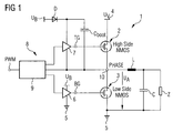
- the Buck converter 1 shown in the circuit of Figure 1 comprises two power switching transistors, a high side NMOS transistor 2 connected to a supply potential line 4, and a low side NMOS transistor 3 connected to a ground line 5. High side and low side transistors 2, 3 are interconnected at a node which is formed by the output 10.
- the switching converter 1 is designed as a half-bridge circuit in which, starting from output 10, an inductance L and a capacitance C are connected in series with ground line 5.
- the two switching transistors 2, 3 are controllable by corresponding gates.
- the corresponding gate terminals, hereafter called the top gate and bottom gate are identified by the reference characters TG and BG.
- Gates TB, BG are controlled by drivers 6, 7 which are interconnected in the known conventional manner.
- Drivers 6, 7, and thus gates TG, BG of switching transistors 2, 3, are controlled by a control device 8, of which only a short circuit detector 9 provided according to the invention is shown in the drawings, the function of this detector being described in detail below.
- PWM signal pulse-width modulated signal
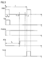
- This signal is identified by the reference notation PWM in Figures 1 through 3.
- the period of the PWM signal is identified by reference notation T in Figures 2 and 3.
- the following discussion is based on a pulse with a time period t p which switches high side NMOS transistor 2 to the conducting state.
- phase position PHASE of the output signal U A is tested at output 10. If it is determined that phase position PHASE has changed after a certain time period T'- t P after pulse PWM has been turned off (corresponding to T' ⁇ T), bottom gate terminal BG is controlled in a fourth step 16, and converter 1 shifts to a normal operational state.
- phase position PHASE of output signal U A at output 10 has not changed (test in third step 15)
- low side transistor 3 is controlled by bottom gate BG and a second counter is started (fourth step 17).
- a test is performed in a fifth step 18 to see whether phase position PHASE at output 10 has changed. If after a certain time T' ' - to (T' ' ⁇ T) it is determined that the phase position has changed, then low side transistor 3 is controlled by bottom gate BG in a sixth step 19, and converter 1 is shifted to a normal operational state.
- step 18 determines that phase position PHASE of output signal U A at output 10 has not changed, this is interpreted by short circuit 9 of control device 8 as a short circuit at high side NMOS transistor 2 (sixth step 20).
- control device 8 initiates a procedure which shifts switching converter 1 to an operationally reliable state.
- a protective signal Prot in the form of a switching pulse is generated.
- This protective signal or safety pulse Prot prevents top gate TG of high side NMOS transistor 2 from being controlled by the following pulse-width-modulated pulse PWM (step 21).
- Control device 8 ensures that bottom gate BT of low side NMOS transistor 3 continues to be controlled, thereby short circuiting output 10 to ground 5. This action prevents supply voltage U V from dropping completely across load Z, thereby destroying it. Instead, the current is diverted through low side transistor 3 to ground 5.
- the invention provides that phase position PHASE be tested once again during the next period T of PWM signal PWM (ninth step 23).
- procedural steps 5 through 9 may cycled through multiple times as required, as indicated by reference numerals 18, 19, 21, 22.
Landscapes
- Engineering & Computer Science (AREA)
- Power Engineering (AREA)
- Dc-Dc Converters (AREA)
Abstract
Description
- The invention relates to a method for controlling a switching converter (switching regulator, switched-mode power supply) comprising a high side switch and a low side switch according to the preamble of
Claim 1, as well as a control device for a switching converter comprising a high side Switch and a low side switch according to the preamble ofClaim 13. - Switching converters include a high side power switch connected to a connection line at a high supply potential which is switched in a clock period of a signal modulated in a pulse width, and generally include a low side power switch connected to a ground line which is switched in a clock pulse of a second signal (possibly derived from the pulse-width-modulated), are known in the prior art in a multiplicity of variations. For examples, reference is made to U. Tietze, Ch. Schenk, "Semiconductor Circuitry" [Halbleiter-Schaltungstechnik] , 10th edition, Springer-Verlag Berlin Heidelberg New York, 1993, pp. 561 et seq.
- The approach is known from company-internal prior art whereby an overvoltage protection device is provided which turns off the high side power switch when the output voltage exceeds a predetermined threshold value.
- Although in principle this measure has proven successful, it has nevertheless been determined that devices connected to Buck converters in particular were destroyed by an overvoltage.
- The goal of the invention is therefore to provide a method for controlling a switching converter comprising a high side switch and a low side switch, as well as a control device for a switching converter comprising a high side switch and low side switch, wherein the occurrence of improper voltages, specifically overvoltages, on the output side is prevented.
- This goal is achieved by a method having the features of
Claim 1 and a device having the features ofClaim 13. - Advantageous embodiments and modifications of the invention are described in the subordinate claims.
- The invention starts with a switching converter, specifically, a step-up converter or a Buck converter of the species described above which has a high side switch and a low side switch, specifically, a bridge circuit or half-bridge circuit.
- The method according to the invention for controlling the switching converter is distinguished by the fact that the high side switch is tested for a short circuit, and that upon detection of a short circuit in the high side switch the switching converter remains in an operationally reliable state (whenever it is already in such a state), or by the fact that the converter is shifted to an operationally reliable state (because and to the extent a danger exists that the high side switch has been destroyed such that the output voltage can no longer be regulated). This measure prevents the loads connected to the output of the converter from being destroyed by an overvoltage.
- The device according to the invention for controlling a switching converter accordingly comprises testing means which test the high side switch for a short circuit, and control means which, upon detection of a short circuit in the high side switch, shift the switching converter to an operationally reliable state or which, upon detection of the short circuit ensure in the high side switch that the switching converter remains in an operationally reliable state - thereby effectively preventing destruction of the load device supplied with a clocked DC voltage by the switching converter.
- In an especially advantageous variant embodiment of the invention, the high side switch is tested for a short circuit by testing for a missing change in the phase position of the output voltage, which is provided by the switching converter and supplies the load device, relative to the corresponding current drawn by the load device in response to a change in the switching state of the high side switch. If it is determined that the phase position of current relative to voltage has not changed, despite the fact that the high side switch has been turned on or off, then this is an indication that the high side switch is defective and that the switch has continued to remain in its state prior to being actuated. As a rule, the switch will be short circuited, for example, because the transistor acting as the switch has been breached. As a result, the full operating voltage is applied at the output of the bridge or half-bridge if the measures according to the teaching of the invention creating an operationally reliable state have not been taken.
- In principle, it is possible to determine the phase position continuously. As a rule, however, this is relatively complicated and also not required for the reliable operation of the switching converter. According to the invention, in an especially advantageous embodiment of the variant described above, a test of the phase position is performed only at a (preferably predetermined) point in time after the switching state of the high side switch has changed. If at this point in time it is determined that the phase position has not changed (or has not changed by some predetermined amount which indicates a short circuit), this is interpreted as a short circuit and appropriate measures are initiated to shift the converter to an operationally reliable state, unless it is already in such a state.
- In order to preclude misinterpretations, the invention provides that the time interval be shorter than the time period until another change in the switching state of the high side switch occurs.
- Although in principle any change in the switching state of the high side switch may be used to analyze the phase position of the output signal, it has proven to be especially advantageous to test the change in the phase position in response to a turning-off of the high side switch. After the turn-off and when the high side switch is operating properly, energy is only drawn from the converter (by the load device), and no energy is supplied to it, with the result that the phase position will change relatively rapidly, whereas after turning on when the high side switch is operating properly energy is both supplied and removed - with the result that in the initial moment after turn-on the phase position may change only very slightly. In the first case, any changes in the phase position are thus detectable with greater sensitivity, and the identification of a short circuit is less prone to error.
- In order to be able to detect a short circuit of the high side switch as such even more reliably, according to the invention the high side switch is alternatively or additionally tested for a short circuit by testing for a missing change in the phase position of the output voltage supplied by the switching converter in response to a change in the switching state of the low side switch. Preferably, the low side switch here is turned on. When the low side switch is turned on, the output terminal of the converter is short circuited to ground. If the high side switch is open, the phase position will change rapidly due to the current draining through the low side switch, whereas no change will occur if the high side switch is open. If the high side switch is open, despite the fact that it is supposed to be closed, this condition can be easily used to detect a short circuit.
- Again, in principle, it is possible to determine the phase position continuously. As a rule, however, it is relatively complicated and also not required for the reliable operation of the switching converter. Thus, according to the invention, as in the above case, a missing change in the phase position after a predetermined time interval after a change in the switching state of the low side switch is interpreted as a short circuit of the high side switch.
- The point in time for determining the phase position is selected, in a manner analogous to the above, so that the time interval for the change in the switching state is smaller than the time period until another change in the switching state of the high side switch occurs.
- Furthermore, according to the invention, the operationally reliable state in which the converter is placed upon detection of a short circuit, or the state in which the converter remains, is the turned-on state of the low side switch. This ensures that the energy drawn by the converter is not delivered to the load device but instead dissipated within the converter itself.
- In an especially advantageous embodiment of the invention, the above described process is implemented repeatedly, and the operationally reliable state in which the converter is found upon detection of a short circuit is vacated only once it has been determined that no short circuit is present in the high side switch.
- The following explains the invention in more detail based on the drawings.
- Figure 1
- is a schematic diagram of one embodiment of a control device according to the invention for a Buck converter in a half-bridge configuration;
- Figure 2
- is a flowchart showing the functional principle of the control device of Figure 1; and
- Figure 3
- shows the signal characteristics within the control device of Figure 1 which implements the functional principle presented in the flowchart of Figure 2.
- The
Buck converter 1 shown in the circuit of Figure 1 comprises two power switching transistors, a high side NMOS transistor 2 connected to a supply potential line 4, and a low side NMOS transistor 3 connected to aground line 5. High side and low side transistors 2, 3 are interconnected at a node which is formed by theoutput 10. Theswitching converter 1 is designed as a half-bridge circuit in which, starting fromoutput 10, an inductance L and a capacitance C are connected in series withground line 5. - The load to be supplied by switching
converter 1 with a voltage, which load is symbolized in the schematic diagram as inductance Z, is connected in parallel to capacitance C toground connection 5 and to inductance L. The two switching transistors 2, 3 are controllable by corresponding gates. In the drawings, the corresponding gate terminals, hereafter called the top gate and bottom gate, are identified by the reference characters TG and BG. - Gates TB, BG are controlled by
drivers 6, 7 which are interconnected in the known conventional manner. -
Drivers 6, 7, and thus gates TG, BG of switching transistors 2, 3, are controlled by a control device 8, of which only ashort circuit detector 9 provided according to the invention is shown in the drawings, the function of this detector being described in detail below. - The functional principle of the circuit shown in Figure 1 will now be explained based on Figures 2 and 3.
- As is conventionally the case with Buck converters, high side transistor 2 is controlled by pulse-width modulated signal (PWM signal). This signal is identified by the reference notation PWM in Figures 1 through 3. The period of the PWM signal is identified by reference notation T in Figures 2 and 3.
- The following discussion is based on a pulse with a time period tp which switches high side NMOS transistor 2 to the conducting state.
- At the end of the pulse, that is, in the case of a trailing edge for pulse PWM, high side NMOS transistor 2 is to be shifted from the conducting state to the nonconducting state (
first step 13 in Figure 2). As a result, a first counter is started in control device 8 (second step 14 in Figure 2). - Subsequently, in a
third step 15, the phase position PHASE of the output signal UA is tested atoutput 10. If it is determined that phase position PHASE has changed after a certain time period T'- tP after pulse PWM has been turned off (corresponding to T'< T), bottom gate terminal BG is controlled in a fourth step 16, and converter 1 shifts to a normal operational state. - If phase position PHASE of output signal UA at
output 10 has not changed (test in third step 15), then low side transistor 3 is controlled by bottom gate BG and a second counter is started (fourth step 17). - After the second counter has started, a test is performed in a fifth step 18 to see whether phase position PHASE at
output 10 has changed. If after a certain time T' ' - to (T' ' <T) it is determined that the phase position has changed, then low side transistor 3 is controlled by bottom gate BG in a sixth step 19, andconverter 1 is shifted to a normal operational state. - If instead fifth step 18 determines that phase position PHASE of output signal UA at
output 10 has not changed, this is interpreted byshort circuit 9 of control device 8 as a short circuit at high side NMOS transistor 2 (sixth step 20). - As a result, control device 8 initiates a procedure which shifts switching
converter 1 to an operationally reliable state. In this embodiment, a protective signal Prot in the form of a switching pulse is generated. This protective signal or safety pulse Prot prevents top gate TG of high side NMOS transistor 2 from being controlled by the following pulse-width-modulated pulse PWM (step 21). - Control device 8 ensures that bottom gate BT of low side NMOS transistor 3 continues to be controlled, thereby
short circuiting output 10 toground 5. This action prevents supply voltage UV from dropping completely across load Z, thereby destroying it. Instead, the current is diverted through low side transistor 3 toground 5. - In order to preclude the possibility that the normal operation of switching
converter 1 remains in this operational safety state due to a misinterpretation of a short circuit in high side NMOS transistor 2, the invention provides that phase position PHASE be tested once again during the next period T of PWM signal PWM (ninth step 23). As a result,procedural steps 5 through 9 may cycled through multiple times as required, as indicated byreference numerals -
- 1
- switching converter
- 2
- high side NMOS transistor
- 3
- low side NMOS transistor
- 4
- supply potential line
- 5
- ground terminal / line
- 6
- driver
- 7
- driver
- 8
- control device
- 9
- short circuit detector
- 10
- output
- 13
- first step
- 14
- second step
- 15
- third step
- 16
- fourth step first alternative
- 17
- fourth step second alternative
- 18
- fifth step
- 19
- sixth step first alternative
- 20
- sixth step second alternative
- 21
- seventh step
- 22
- eighth step
- 23
- ninth step = fifth step
- UB
- operating voltage of the control circuit
- UV
- supply voltage
- UA
- output voltage
- TG
- top gate terminal
- BG
- bottom gate terminal
- t
- time
- tP
- pulse period
- to
- time
- Z
- load
- L
- inductance
- C
- capacitance
- Cboot
- capacitance
- D
- diode
- PWM
- pulse-width modulated signal (PWM signal)
- PHASE
- phase position
- Prot
- safety pulse
- T
- period of the PWM signal
- T'
- first time period
- T' '
- second time period
Claims (24)
- Method for controlling a switching converter (1), comprising a high side switch (2) and a low side switch (3),
characterized in that
the high side switch (2) is tested for a short circuit, and that upon detection (20) of a short circuit in the high side switch (2) the switching converter (1) remains in an operationally reliable state or is shifted to an operationally reliable state. - Method according to Claim 1,
characterized in that
the high side switch (2) is tested for a short circuit by an approach in which a test is performed for a missing change in a phase position (PHASE) of an output voltage (UA) provided by the switching converter (1) in response to a change in the switching state of the high side switch (2). - Method according to Claim 2,
characterized in that
a short circuit exists if the phase position (PHASE) has not changed after a predetermined time interval (T' - tp) has been exceeded after a change in the switching state of the high side switch (2). - Method according to Claim 3,
characterized in that
the time interval (T' - tP) is smaller than a time period (T - tP) until another change in the switching state of the high side switch (2) occurs. - Method according to one of Claims 2 through 4,
characterized in that
the change in the switching state is the turn-off for the high side switch (2). - Method according to one of the foregoing claims,
characterized in that
the high side switch (2) is tested alternatively or additionally for a short circuit by an approach in which a test is performed for a missing change in a phase position (PHASE) of the output voltage (UA) provided by the switching converter (1) in response to a change in the switching state of the high side switch (3). - Method according to Claim 6,
characterized in that
the system decides that a short circuit exists if the phase position (PHASE) has not changed after a predetermined time interval (T' ' - to) has been exceeded after a change in the switching state of the low side switch (3). - Method according to Claim 7,
characterized in that
the time interval (T' ' - to) is smaller than a time period (T - tp) until an additional change in the switching state of the high side switch (2) occurs. - Method according to one of Claims 6 through 8,
characterized in that
the change in the switching state is the turning-on of the low side switch (3). - Method according to Claim 9,
characterized in that
the turning-on of the low side switch (3) occurs after the turning-off of the high side switch (2). - Method according to one of the foregoing claims,
characterized in that
upon detection (20) of a short circuit the low side switch (3) is turned on or remains in the turned-on state. - Method according to one of the foregoing claims,
characterized in that
the method according to one of Claims 1 through 11 is implemented repeatedly. - Control device (8) for a switching converter (1), comprising a high side switch (2) and a low side switch (3),
characterized in that
testing means (9) are provided which test the high side switch (2) for a short circuit, and control means are provided which, upon detection (20) of a short circuit in the high side switch (2), shift the switching converter (1) to an operationally reliable state, or upon detection (20) of the short circuit in the high side switch (2) control the switching converter (1) such that it remains in an operationally reliable state. - Control device (8) according to Claim 13,
characterized in that
the testing means (9) test the high side switch (2) by an approach in which said means test for a missing change in a phase position (PHASE) of an output voltage (UA) provided by the switching converter (1) in response to a change in the switching state of the high side switch (2). - Control device (8) according to Claim 14,
characterized in that
the testing means (9) decide that a short circuit exists if the phase position (PHASE) has not changed after a predetermined time interval (T' - tP) has been exceeded after a change in the switching state of the high side switch (2). - Control device (8) according to Claim 15,
characterized in that
the time interval (T' - tP) is smaller than a time period (T - tP) until another change in the switching state of the high side switch (2) occurs. - Control device (8) according to one of Claims 14 through 16,
characterized in that
the change in the switching state is the turn-off for the high side switch (2). - Control device (8) according to one of Claims 13 through 17,
characterized in that
the testing means (9) test the high side switch (2) alternatively or additionally for a short circuit by an approach in which they (9) test for a missing change of a phase position (PHASE) of the output voltage (UA) provided by the switching converter (1) in response to a change in the switching state of the low side switch (3). - Control device (8) according to Claim 18,
characterized in that
a short circuit exists if the phase position (PHASE) has not changed after a predetermined time interval (T' ' - to) has been exceeded after a change in the switching state of the low side switch (3). - Control device (8) according to Claim 19,
characterized in that
the time interval (T' ' - to) is smaller than a time (T - tP) until an additional change in the switching state of the high side switch (2) occurs. - Control device (8) according to one of Claims 18 through 20,
characterized in that
the change in the switching state is the turning-on of the low side switch (3). - Control device (8) according to Claim 21,
characterized in that
the turning-on of the low side switch (3) occurs after the turning-off of the high side switch (2). - Control device (8) according to one of Claims 13 through 22,
characterized in that
the control means switch the low side switch (3) in response to the detection (20) of a short circuit, or control the low side switch (3) so that it remains in the turned-on state. - Control device (8) according to one of Claims 13 through 22,
characterized in that
the control device (8) is designed repeatedly to implement the method according to one of Claims 1 through 11.
Priority Applications (3)
| Application Number | Priority Date | Filing Date | Title |
|---|---|---|---|
| EP04018484A EP1624559B1 (en) | 2004-08-04 | 2004-08-04 | Method for controlling a switching converter and control device for a switching converter |
| DE602004029667T DE602004029667D1 (en) | 2004-08-04 | 2004-08-04 | Method for controlling a clocked converter and control device for a clocked converter |
| US11/198,866 US7199589B2 (en) | 2004-08-04 | 2005-08-04 | Method for controlling a switching converter and control device for a switching converter |
Applications Claiming Priority (1)
| Application Number | Priority Date | Filing Date | Title |
|---|---|---|---|
| EP04018484A EP1624559B1 (en) | 2004-08-04 | 2004-08-04 | Method for controlling a switching converter and control device for a switching converter |
Publications (2)
| Publication Number | Publication Date |
|---|---|
| EP1624559A1 true EP1624559A1 (en) | 2006-02-08 |
| EP1624559B1 EP1624559B1 (en) | 2010-10-20 |
Family
ID=34926050
Family Applications (1)
| Application Number | Title | Priority Date | Filing Date |
|---|---|---|---|
| EP04018484A Expired - Lifetime EP1624559B1 (en) | 2004-08-04 | 2004-08-04 | Method for controlling a switching converter and control device for a switching converter |
Country Status (3)
| Country | Link |
|---|---|
| US (1) | US7199589B2 (en) |
| EP (1) | EP1624559B1 (en) |
| DE (1) | DE602004029667D1 (en) |
Cited By (1)
| Publication number | Priority date | Publication date | Assignee | Title |
|---|---|---|---|---|
| US7557637B2 (en) | 2006-03-20 | 2009-07-07 | Hitachi, Ltd. | Semiconductor circuit |
Families Citing this family (7)
| Publication number | Priority date | Publication date | Assignee | Title |
|---|---|---|---|---|
| US7593200B2 (en) * | 2006-08-15 | 2009-09-22 | International Rectifier Corporation | Buck converter fault detection method |
| DE102006045308B4 (en) * | 2006-09-26 | 2011-07-21 | Continental Automotive GmbH, 30165 | Circuit arrangement for detecting the state of a load device which can be connected to a switching connection and method for operating such a circuit arrangement |
| JP2013013297A (en) * | 2011-06-30 | 2013-01-17 | Jtekt Corp | Vehicular steering system |
| US20150091539A1 (en) * | 2013-10-02 | 2015-04-02 | Infineon Technologies Autria AG | Half-bridge gate driver control |
| CN103929046B (en) * | 2014-04-24 | 2016-03-30 | 东南大学 | Switching tube failure detector circuit in a kind of BUCK Topology Switch power supply |
| US10024889B2 (en) * | 2015-12-23 | 2018-07-17 | Intel IP Corporation | Apparatuses, methods, and systems for detection of a current level |
| JP7294084B2 (en) * | 2019-11-25 | 2023-06-20 | 株式会社デンソー | Short circuit detection device |
Citations (1)
| Publication number | Priority date | Publication date | Assignee | Title |
|---|---|---|---|---|
| US20040124818A1 (en) * | 2002-12-31 | 2004-07-01 | Intersil Americas Inc., | Mechanism for providing over-voltage protection during power up of DC-DC converter |
Family Cites Families (5)
| Publication number | Priority date | Publication date | Assignee | Title |
|---|---|---|---|---|
| DE19628131C2 (en) * | 1996-07-12 | 2003-07-17 | Semikron Elektronik Gmbh | Gate voltage limitation for a circuit arrangement |
| JP4074697B2 (en) * | 1997-11-28 | 2008-04-09 | 株式会社ルネサステクノロジ | Semiconductor device |
| EP1279042A2 (en) * | 2000-04-26 | 2003-01-29 | Koninklijke Philips Electronics N.V. | Electronic circuit device with a short circuit switch and method of testing such a device |
| US6741116B2 (en) * | 2001-10-15 | 2004-05-25 | Semikron Elekronik Gmbh | Semiconductor component for direct gate control and monitoring of power semiconductor switches |
| US6930500B2 (en) * | 2003-08-01 | 2005-08-16 | Board Of Supervisors Of Louisiana State University And Agricultural And Mechanical College | IDDQ testing of CMOS mixed-signal integrated circuits |
-
2004
- 2004-08-04 DE DE602004029667T patent/DE602004029667D1/en not_active Expired - Lifetime
- 2004-08-04 EP EP04018484A patent/EP1624559B1/en not_active Expired - Lifetime
-
2005
- 2005-08-04 US US11/198,866 patent/US7199589B2/en not_active Expired - Lifetime
Patent Citations (1)
| Publication number | Priority date | Publication date | Assignee | Title |
|---|---|---|---|---|
| US20040124818A1 (en) * | 2002-12-31 | 2004-07-01 | Intersil Americas Inc., | Mechanism for providing over-voltage protection during power up of DC-DC converter |
Cited By (1)
| Publication number | Priority date | Publication date | Assignee | Title |
|---|---|---|---|---|
| US7557637B2 (en) | 2006-03-20 | 2009-07-07 | Hitachi, Ltd. | Semiconductor circuit |
Also Published As
| Publication number | Publication date |
|---|---|
| US7199589B2 (en) | 2007-04-03 |
| EP1624559B1 (en) | 2010-10-20 |
| US20060055380A1 (en) | 2006-03-16 |
| DE602004029667D1 (en) | 2010-12-02 |
Similar Documents
| Publication | Publication Date | Title |
|---|---|---|
| US10756634B2 (en) | Systems and methods for protecting power conversion systems under open and/or short circuit conditions | |
| US7420355B2 (en) | DC-DC converter with over-voltage protection | |
| JP4267865B2 (en) | Load drive device | |
| CN111327024B (en) | Protection circuit with cut-off switch for power system | |
| CN102045047B (en) | Semiconductor device | |
| DE102009029402B4 (en) | Overload protection for a circuit arrangement with a transistor | |
| US8593773B2 (en) | Half-bridge circuit protected against short circuits and having semiconductor switches | |
| US11171559B2 (en) | Overcurrent protection detector with dynamic threshold for power conversion switch | |
| US11056969B2 (en) | Boost converter short circuit protection | |
| US6330143B1 (en) | Automatic over-current protection of transistors | |
| EP1624559B1 (en) | Method for controlling a switching converter and control device for a switching converter | |
| CN114303309B (en) | Overcurrent protection circuit and switch circuit | |
| KR20210070591A (en) | Short circuit protection for power switch | |
| US10536088B2 (en) | Switched mode power supply controller | |
| WO2005091482A1 (en) | Dc-dc converter | |
| US20080198525A1 (en) | Method for Current Protection of a Power Switch and Apparatus for Implementing Same | |
| JP6566261B2 (en) | Earth leakage breaker | |
| US11108226B1 (en) | Method and apparatus for reverse over current protection | |
| CN115280656A (en) | Protection circuit for high inductive loads | |
| US5764466A (en) | Circuit for short circuit detection through resistive shunt in power circuits using unipolar control voltage | |
| EP2978116A1 (en) | DC/DC converter circuit | |
| KR20230055364A (en) | Apparatus for protecting a short in a switch | |
| US12525909B2 (en) | Motor drive circuitry | |
| EP3993264A1 (en) | Switch controller, device and method with overcurrent protection | |
| JP2004343426A (en) | Dither current control circuit for solenoid |
Legal Events
| Date | Code | Title | Description |
|---|---|---|---|
| PUAI | Public reference made under article 153(3) epc to a published international application that has entered the european phase |
Free format text: ORIGINAL CODE: 0009012 |
|
| AK | Designated contracting states |
Kind code of ref document: A1 Designated state(s): AT BE BG CH CY CZ DE DK EE ES FI FR GB GR HU IE IT LI LU MC NL PL PT RO SE SI SK TR |
|
| AX | Request for extension of the european patent |
Extension state: AL HR LT LV MK |
|
| 17P | Request for examination filed |
Effective date: 20060215 |
|
| AKX | Designation fees paid |
Designated state(s): DE FR GB IT |
|
| 17Q | First examination report despatched |
Effective date: 20090904 |
|
| GRAP | Despatch of communication of intention to grant a patent |
Free format text: ORIGINAL CODE: EPIDOSNIGR1 |
|
| RAP1 | Party data changed (applicant data changed or rights of an application transferred) |
Owner name: INFINEON TECHNOLOGIES AG |
|
| GRAS | Grant fee paid |
Free format text: ORIGINAL CODE: EPIDOSNIGR3 |
|
| GRAA | (expected) grant |
Free format text: ORIGINAL CODE: 0009210 |
|
| AK | Designated contracting states |
Kind code of ref document: B1 Designated state(s): DE FR GB IT |
|
| REG | Reference to a national code |
Ref country code: GB Ref legal event code: FG4D |
|
| REF | Corresponds to: |
Ref document number: 602004029667 Country of ref document: DE Date of ref document: 20101202 Kind code of ref document: P |
|
| PLBE | No opposition filed within time limit |
Free format text: ORIGINAL CODE: 0009261 |
|
| STAA | Information on the status of an ep patent application or granted ep patent |
Free format text: STATUS: NO OPPOSITION FILED WITHIN TIME LIMIT |
|
| 26N | No opposition filed |
Effective date: 20110721 |
|
| REG | Reference to a national code |
Ref country code: DE Ref legal event code: R097 Ref document number: 602004029667 Country of ref document: DE Effective date: 20110721 |
|
| REG | Reference to a national code |
Ref country code: FR Ref legal event code: PLFP Year of fee payment: 13 |
|
| REG | Reference to a national code |
Ref country code: FR Ref legal event code: PLFP Year of fee payment: 14 |
|
| REG | Reference to a national code |
Ref country code: FR Ref legal event code: PLFP Year of fee payment: 15 |
|
| PGFP | Annual fee paid to national office [announced via postgrant information from national office to epo] |
Ref country code: IT Payment date: 20220825 Year of fee payment: 19 Ref country code: GB Payment date: 20220822 Year of fee payment: 19 |
|
| PGFP | Annual fee paid to national office [announced via postgrant information from national office to epo] |
Ref country code: FR Payment date: 20220823 Year of fee payment: 19 |
|
| PGFP | Annual fee paid to national office [announced via postgrant information from national office to epo] |
Ref country code: DE Payment date: 20221021 Year of fee payment: 19 |
|
| P01 | Opt-out of the competence of the unified patent court (upc) registered |
Effective date: 20230528 |
|
| REG | Reference to a national code |
Ref country code: DE Ref legal event code: R119 Ref document number: 602004029667 Country of ref document: DE |
|
| GBPC | Gb: european patent ceased through non-payment of renewal fee |
Effective date: 20230804 |
|
| PG25 | Lapsed in a contracting state [announced via postgrant information from national office to epo] |
Ref country code: GB Free format text: LAPSE BECAUSE OF NON-PAYMENT OF DUE FEES Effective date: 20230804 |
|
| PG25 | Lapsed in a contracting state [announced via postgrant information from national office to epo] |
Ref country code: IT Free format text: LAPSE BECAUSE OF NON-PAYMENT OF DUE FEES Effective date: 20230804 Ref country code: GB Free format text: LAPSE BECAUSE OF NON-PAYMENT OF DUE FEES Effective date: 20230804 Ref country code: FR Free format text: LAPSE BECAUSE OF NON-PAYMENT OF DUE FEES Effective date: 20230831 Ref country code: DE Free format text: LAPSE BECAUSE OF NON-PAYMENT OF DUE FEES Effective date: 20240301 |