EP1624537A2 - Screened surge arrester - Google Patents
Screened surge arrester Download PDFInfo
- Publication number
- EP1624537A2 EP1624537A2 EP05254722A EP05254722A EP1624537A2 EP 1624537 A2 EP1624537 A2 EP 1624537A2 EP 05254722 A EP05254722 A EP 05254722A EP 05254722 A EP05254722 A EP 05254722A EP 1624537 A2 EP1624537 A2 EP 1624537A2
- Authority
- EP
- European Patent Office
- Prior art keywords
- electrode
- connector
- component
- arrangement according
- electrical
- Prior art date
- Legal status (The legal status is an assumption and is not a legal conclusion. Google has not performed a legal analysis and makes no representation as to the accuracy of the status listed.)
- Granted
Links
Images


Classifications
-
- H—ELECTRICITY
- H01—ELECTRIC ELEMENTS
- H01R—ELECTRICALLY-CONDUCTIVE CONNECTIONS; STRUCTURAL ASSOCIATIONS OF A PLURALITY OF MUTUALLY-INSULATED ELECTRICAL CONNECTING ELEMENTS; COUPLING DEVICES; CURRENT COLLECTORS
- H01R13/00—Details of coupling devices of the kinds covered by groups H01R12/70 or H01R24/00 - H01R33/00
- H01R13/46—Bases; Cases
- H01R13/53—Bases or cases for heavy duty; Bases or cases for high voltage with means for preventing corona or arcing
-
- H—ELECTRICITY
- H01—ELECTRIC ELEMENTS
- H01C—RESISTORS
- H01C7/00—Non-adjustable resistors formed as one or more layers or coatings; Non-adjustable resistors made from powdered conducting material or powdered semi-conducting material with or without insulating material
- H01C7/10—Non-adjustable resistors formed as one or more layers or coatings; Non-adjustable resistors made from powdered conducting material or powdered semi-conducting material with or without insulating material voltage responsive, i.e. varistors
- H01C7/12—Overvoltage protection resistors; Arresters
- H01C7/126—Means for protecting against excessive pressure or for disconnecting in case of failure
-
- H—ELECTRICITY
- H01—ELECTRIC ELEMENTS
- H01R—ELECTRICALLY-CONDUCTIVE CONNECTIONS; STRUCTURAL ASSOCIATIONS OF A PLURALITY OF MUTUALLY-INSULATED ELECTRICAL CONNECTING ELEMENTS; COUPLING DEVICES; CURRENT COLLECTORS
- H01R13/00—Details of coupling devices of the kinds covered by groups H01R12/70 or H01R24/00 - H01R33/00
- H01R13/66—Structural association with built-in electrical component
- H01R13/665—Structural association with built-in electrical component with built-in electronic circuit
- H01R13/6666—Structural association with built-in electrical component with built-in electronic circuit with built-in overvoltage protection
Definitions
- This invention relates to a high voltage connector arrangement, and finds particular, though not exclusive, application to the connection of a surge arrester to electrical switchgear.
- surge arresters employing air gaps are known, surge arresters using varistor, and especially metal oxide varistor (MOV), blocks are commonly used.
- MOV metal oxide varistor
- a surge arrester comprises a plurality of substantially solid cylindrical blocks of MOV material compressed in end-to-end relationship between a pair of cylindrical metal electrodes, all sealingly encased within a insulating house, for example of silicone polymer. A conductive coating is then applied to the outer polymer surface to provide the required screening.
- the present invention provides a high voltage connector arrangement comprising an elongate electrically insulated device, which may be an insulated and screened surge arrester module, and an insulated connector for connecting the device to electrical equipment, which may be switchgear.
- the arrangement may be such that components of the device are protected from excess current flow therethrough, or the electrical field at the connector end of the screen of the device is reduced. In a preferred embodiment, the arrangement can achieve both of these results.
- the protection of the device is achieved by placing an electrode of the device within an insulated, and advantageously screened, arm of the connector adjacent the end of the screen of the device.
- the electrode may comprise the electrode at one end of the device or may be spaced therefrom, for example by a component of the device.
- the electrical field stress may be reduced by suitable shaping of the electrode at the end of the conductive screen of the device.
- a high voltage connector arrangement comprising:
- the device and in particular its said other electrode, and the connector arm are of generally cylindrical configuration.
- the positioning of the said other electrode of the device is such that short circuit current is encouraged to pass from that electrode, through the adjacent wall of the insulating material of the device to its conductive layer and hence to the other electrode, rather than passing through the component in the interior of the device.
- a high voltage connector arrangement comprising:
- An arrangement in accordance with the present invention may be such that the device comprises a further electrical component and a further electrode enclosed within the insulating material, wherein the further electrode is disposed at the end of the device remote from said one end, and wherein the further component is disposed between the further electrode and the said other electrode.
- the shaping of the said other electrode reduces electrical stress within the connector in the region of the device, and particularly at the enclosed end of the conductive screening layer, and preferably comprises an inwardly-directed tapering thereof.
- the arrangement of the present invention comprises features of both aspects thereof.
- the insulated connector of the arrangement is electrically screened, the screening of the arm thereof enclosing the electrical device and advantageously overlapping the screening layer of the device.
- the insulating material used in the arrangement of the invention is silicone polymer.
- the sealing engagement of the device within the connector can be achieved as a push-fit, allowing for convenient demountability when required.
- a known high voltage connector arrangement comprises a T-shaped screened connector 2 and an elongate cylindrical surge arrester module 4.
- the connector 2 comprises an insulating housing 5 of silicone polymer that defines a transverse passageway 6, and a further passageway 8 extending at right angles thereto.
- the passageway 6 is terminated at one end by a flange 10 for mounting the connector 2 onto a bushing of switchgear (not shown).
- the other end of the passageway 6 is closed by a cap 12.
- the surge arrester module 4 comprises a lower electrode 14, an upper electrode 16, and a plurality of MOV varister blocks 18 extending end to end between the electrodes.
- the electrode and MOV block structure is held together longitudinally in compression (by means not shown) and is enclosed within silicone rubber insulation 20, with a lower terminal 22 protruding therefrom and a connecting lug 24 protruding from the upper electrode 16.
- the surge arrester module 4 is push-fitted into a depending arm 26 of the housing 5 of the connector 2 that contains the passageway 8, such that the connecting lug 24 projects into the passageway 6 and is secured therein to a metal plate 28 by a transverse bolt 30.
- the connector housing 5 is electrically screened by means of a conductive coating 32 on the outer surface thereof, which is connected to a terminating pigtail 34 for connection to earth.
- the surge arrester module 4 is also screened by a conductive coating 36 that extends from the lower end thereof and terminates partway along the stack of MOV blocks 18 at its upper end 38 within the connector arm 26.
- the location within the connector arm 26 of the termination 38 of the surge arrester screen 36 is typically 5 to 10mm from the end of the arm 36, this providing a working tolerance to ensure that the screen 36 is enclosed by the arm 26.
- a conductive coating 40 extends around the inside of the passageway 8 so as to enclose the connecting lug 24 of the surge arrester module 4 within a Faraday Cage.
- the flange 10 of the connector 2 is mounted onto a bushing of the switchgear, thereby establishing an electrical connection via the bolt 30 to the surge arrester module 4.
- the electrical field at the termination 38 of the surge arrester screen 36, within the screened insulating arm 26 of the connector 2, can be unacceptably high.
- the short circuit current performance is poor, allowing a high current to flow between the upper electrode 16 and the lower electrode 14 through the MOV blocks 18. Under these circumstances, the surge arrester module 4 can fail explosively and unacceptably.
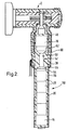
- the primary difference with the arrangement of Figure 2 lies in the construction of its surge arrester module 50, in that as well as the lower and upper electrodes 14 and 16 respectively and the stack of MOV blocks 18, an additional electrode 52 is introduced between the upper MOV block 18 and the upper electrode 16, comprehensively longitudinally retained therebetween.
- the positioning of the upper electrode 16 within the connector 2 is substantially the same as with the known arrangement shown in Figure 1.
- the additional electrode 52 thus extends downwardly within the surge arrester module 50 so as to dispose its lower end 54 within that portion of the surge arrester insulation 20 that is enclosed within the conductive screen 36. By this means, the electrical field at the upper termination 38 of the arrester screen 36 can be significantly reduced.
- the reduction of the field in this region is achieved by providing the upper portion of the lower end 54 of the electrode 52 with an inwardly directed shoulder 56 that leads to a waisted electrode portion 58 that then tapers outwardly at a shoulder 60 to the upper end 62 of the additional electrode 52.
- the tapered shoulder 60 at the upper end of electrode 52 lies within the region of the lower termination of the Faraday Cage 40 of the connector 2, thus reducing the electrical field strength in that region of the connector arrangement.
- the arrangement shown in Figure 2 also has the advantage of improving the short circuit performance. Under conditions of short circuit, when a large current is applied to the arrangement, it has been found that the current flows from the upper electrode 16, through the additional electrode 52, and thence, rather than directly through the MOV blocks 18, outwardly through the insulating wall 20, to and along the conductive screen 36, and thence back through the insulating wall 20 at its lower end onto the lower electrode 14. Whilst this can itself still lead to explosive failure of the connection arrangement, the explosive effect is significantly less drastic than with the arrangement of Figure 1, giving rise to an acceptable failure mode.
- the additional electrode 52 is shown as a separate component from the upper electrode 16, it is envisaged that these could be formed as a single structure.
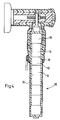
- FIG 3 shows a modification of the arrangement of Figure 2, in that a surge arrester module 70 is provided with an additional upper electrode 72 that is of the same general configuration as the electrode 52 of the Figure 2 embodiment, accept in so far as it does not extend longitudinally from the upper end of the stack of MOV blocks 18 all the way to the upper electrode 16, but is spaced therefrom by the interpositioning of a further MOV block 74. It will be appreciated that the control of the electrical stress at the upper end 38 of the surge arrester screen 36 and the enhanced short circuit performance of the arrester 70 is effected in the same way as previously, resulting from the similar location of the additional electrode 72.
- Figure 4 shows a further embodiment of the invention, in which a surger arrester module 80 is provided with an intermediate additional electrode 82, again longitudinally spaced by a varister block 74 from the upper electrode 16, but in which the intermediate electrode 82 is of substantially right cylindrical configuration, thus providing for the short circuit protection of the varistor blocks 18 of the module 80 due to the positioning of the electrode 82 adjacent the screen end 38.
- the electrical device may have other functions and, for example, could be provided as a monitoring device.
Landscapes
- Engineering & Computer Science (AREA)
- Microelectronics & Electronic Packaging (AREA)
- Physics & Mathematics (AREA)
- Electromagnetism (AREA)
- Thermistors And Varistors (AREA)
- Emergency Protection Circuit Devices (AREA)
- Cable Accessories (AREA)
- Coupling Device And Connection With Printed Circuit (AREA)
Abstract
Description
- This invention relates to a high voltage connector arrangement, and finds particular, though not exclusive, application to the connection of a surge arrester to electrical switchgear.
- It is known to provide an L-, or T-, shaped insulated connector for connecting a cable termination, for example, to electrical equipment, such as switchgear for example. At high voltage, say above about 15kV, and at 24kV and above in particular, it is also known to screen such connectors, that is to say to provide an electrically conductive layer on the outer surface thereof for use with a termination for a screened cable. Such a screened connector is available under the trade name RSTI from Tyco Electronics Raychem GmbH. Screening has the advantages of rendering connectors touchproof and of allowing several connectors, for example one for each phase of a three-phase power supply, to be mounted more closely together, thus reducing the size of the cabinet in which they are contained.
- Difficulties have been encountered however, in producing a suitable high voltage connector arrangement for certain electrical devices, such as surge arresters. Whilst surge arresters employing air gaps are known, surge arresters using varistor, and especially metal oxide varistor (MOV), blocks are commonly used. Typically such a surge arrester comprises a plurality of substantially solid cylindrical blocks of MOV material compressed in end-to-end relationship between a pair of cylindrical metal electrodes, all sealingly encased within a insulating house, for example of silicone polymer. A conductive coating is then applied to the outer polymer surface to provide the required screening. It has been found that securing the screened surge arrester in one arm of a connector, for connection via another arm to switchgear, however, results in unacceptably high electrical field stresses and poor short circuit performance, at high voltage. In the first-mentioned case, a discontinuity in the electrical field distribution arises at the end of the conductive screening layer within the connector, resulting in an unacceptably high electrical field at the interface between the surge arrester and the connector. In the second-mentioned case, in the event of high current flowing through the arrangement, a resulting electric arc passes from one electrode of the surge arrester to the other electrode through the varistor blocks. At sufficiently high energy, this can result in unacceptable explosive destruction of the arrangement.
- It is an object of the present invention to provide a high voltage connector arrangement for connecting a screened electrical device, such as a surge arrester, to electrical equipment, such as switchgear, having improved performance.
- The present invention provides a high voltage connector arrangement comprising an elongate electrically insulated device, which may be an insulated and screened surge arrester module, and an insulated connector for connecting the device to electrical equipment, which may be switchgear. The arrangement may be such that components of the device are protected from excess current flow therethrough, or the electrical field at the connector end of the screen of the device is reduced. In a preferred embodiment, the arrangement can achieve both of these results. The protection of the device is achieved by placing an electrode of the device within an insulated, and advantageously screened, arm of the connector adjacent the end of the screen of the device. The electrode may comprise the electrode at one end of the device or may be spaced therefrom, for example by a component of the device. The electrical field stress may be reduced by suitable shaping of the electrode at the end of the conductive screen of the device.
- In accordance with one aspect of the present invention, there is provided a high voltage connector arrangement comprising:
- an elongate electrically insulated device, and an insulated connector for connecting the device to electrical equipment, wherein
- the device comprises an electrical component and an electrode at each end of and in contact with the component, the component and the electrodes being enclosed within electrically insulating material, a layer of electrically conductive material being applied over the insulating material so as to extend from one end of the device to enclose one of the electrodes and the component and to overlap the other electrode, thereby extending only partway along the length of the device, and wherein
- the device is sealingly inserted in an electrically insulating arm of the connector such that the exposed insulating surface and a portion of the adjoining conductive surface of the device are enclosed within the connector and such that the insulating arm of the connector overlaps the said overlap of the device.
- Advantageously, the device, and in particular its said other electrode, and the connector arm are of generally cylindrical configuration.
- Thus, in the arrangement of the present invention, the positioning of the said other electrode of the device, that is to say that electrode which is disposed within the connector, is such that short circuit current is encouraged to pass from that electrode, through the adjacent wall of the insulating material of the device to its conductive layer and hence to the other electrode, rather than passing through the component in the interior of the device.
- In accordance with another aspect of the present invention, there is provided a high voltage connector arrangement comprising:
- an elongate electrically insulated device, and an insulated connector for connecting the device to electrical equipment, wherein
- the device comprises an electrical component and an electrode at each end of and in contact with the component, the component and the electrodes being enclosed within electrically insulating material and a layer of electrically conductive material being applied over the insulating material so as to extend from one end of the device to enclose one of the electrodes and the component and to overlap the other electrode, thereby extending only partway along the length of the device, wherein the said other electrode extends longitudinally away from the component and is shaped so as to reduce electrical stress at the end of the conductive material, and wherein the device is sealingly inserted in an electrically insulating arm of the connector such that the exposed insulating surface and a portion of the adjoining conductive surface of the device are enclosed within the connector such that the insulating arm thereof overlaps the said overlap of the device.
- An arrangement in accordance with the present invention may be such that the device comprises a further electrical component and a further electrode enclosed within the insulating material, wherein the further electrode is disposed at the end of the device remote from said one end, and wherein the further component is disposed between the further electrode and the said other electrode.
- The shaping of the said other electrode reduces electrical stress within the connector in the region of the device, and particularly at the enclosed end of the conductive screening layer, and preferably comprises an inwardly-directed tapering thereof.
- Advantageously, the arrangement of the present invention comprises features of both aspects thereof.
- In accordance with a further aspect of the present invention, there is provided a method of reducing electrical stress at the end of a conductive layer of an elongate electrically insulated device that is sealingly mounted in an insulated connector for connection to electrical equipment, wherein:
- insulating material is applied to the device so as to surround an electrode at each end thereof and an electrical component that extends between the electrodes;
- conductive material is applied to the device on top of the insulating material so as to extend from enclosing one electrode at one end thereof to enclose the component and to terminate partway along enclosing the other electrode, and wherein the device is inserted into the connector such that the insulation of the connector overlaps the conductive material on the device.
- In accordance with yet another aspect of the present invention, there is provided a method of reducing electrical stress at the end of a conductive layer of an elongate electrically insulated device that is sealingly mounted in an insulated connector for connection to electrical equipment, wherein:
- insulating material is applied to the device so as to surround an electrode at each end thereof and an electrical component that extends between the electrodes,
- conductive material is applied to the device on top of the insulating material so as to extend from enclosing one electrode at one end thereof to enclose the component and to terminate partway along enclosing the other electrode, and wherein the said other electrode is shaped where it extends longitudinally away from the component to reduce electrical stress at the adjacent end of the conductive material on the device.
- Preferably, the insulated connector of the arrangement is electrically screened, the screening of the arm thereof enclosing the electrical device and advantageously overlapping the screening layer of the device.
- Advantageously, the insulating material used in the arrangement of the invention is silicone polymer. The sealing engagement of the device within the connector can be achieved as a push-fit, allowing for convenient demountability when required.
- A high voltage connector arrangement in accordance with the present invention will now be described, by way of example, with reference to the accompanying drawings, in which:
- Figure 1 is a sectional elevation of a conventional connector arrangement including a MOV surge arrester;
- Figure 2 is a sectional elevation of a first embodiment of a connector arrangement in accordance with the present invention;
- Figure 3 is a sectional elevation of a second embodiment of a connector arrangement in accordance with the present invention; and
- Figure 4 is a sectional elevation of a third embodiment of a connector arrangement in accordance with the present invention.
- Referring to Figure 1, a known high voltage connector arrangement comprises a T-shaped screened connector 2 and an elongate cylindrical surge arrester module 4.
- The connector 2 comprises an
insulating housing 5 of silicone polymer that defines atransverse passageway 6, and afurther passageway 8 extending at right angles thereto. Thepassageway 6 is terminated at one end by aflange 10 for mounting the connector 2 onto a bushing of switchgear (not shown). The other end of thepassageway 6 is closed by acap 12. - The surge arrester module 4 comprises a
lower electrode 14, anupper electrode 16, and a plurality ofMOV varister blocks 18 extending end to end between the electrodes. - The electrode and MOV block structure is held together longitudinally in compression (by means not shown) and is enclosed within
silicone rubber insulation 20, with a lower terminal 22 protruding therefrom and a connectinglug 24 protruding from theupper electrode 16. The surge arrester module 4 is push-fitted into a dependingarm 26 of thehousing 5 of the connector 2 that contains thepassageway 8, such that the connectinglug 24 projects into thepassageway 6 and is secured therein to ametal plate 28 by atransverse bolt 30. Theconnector housing 5 is electrically screened by means of aconductive coating 32 on the outer surface thereof, which is connected to a terminatingpigtail 34 for connection to earth. The surge arrester module 4 is also screened by aconductive coating 36 that extends from the lower end thereof and terminates partway along the stack of MOV blocks 18 at itsupper end 38 within theconnector arm 26. The location within theconnector arm 26 of thetermination 38 of thesurge arrester screen 36 is typically 5 to 10mm from the end of thearm 36, this providing a working tolerance to ensure that thescreen 36 is enclosed by thearm 26. - A
conductive coating 40 extends around the inside of thepassageway 8 so as to enclose the connectinglug 24 of the surge arrester module 4 within a Faraday Cage. - In operation, the
flange 10 of the connector 2 is mounted onto a bushing of the switchgear, thereby establishing an electrical connection via thebolt 30 to the surge arrester module 4. - However, it has been found that with this arrangement operating at high voltage, the electrical field at the
termination 38 of thesurge arrester screen 36, within the screenedinsulating arm 26 of the connector 2, can be unacceptably high. Furthermore, it has been found that the short circuit current performance is poor, allowing a high current to flow between theupper electrode 16 and thelower electrode 14 through the MOV blocks 18. Under these circumstances, the surge arrester module 4 can fail explosively and unacceptably. - Reference will now be made to Figure 2, which shows modifications to the arrangement of the connector of Figure 1 that overcome, or at least alleviate, these difficulties. Where applicable, the same reference numerals are employed.
- The primary difference with the arrangement of Figure 2 lies in the construction of its
surge arrester module 50, in that as well as the lower andupper electrodes additional electrode 52 is introduced between theupper MOV block 18 and theupper electrode 16, comprehensively longitudinally retained therebetween. The positioning of theupper electrode 16 within the connector 2 is substantially the same as with the known arrangement shown in Figure 1. Theadditional electrode 52 thus extends downwardly within thesurge arrester module 50 so as to dispose itslower end 54 within that portion of thesurge arrester insulation 20 that is enclosed within theconductive screen 36. By this means, the electrical field at theupper termination 38 of thearrester screen 36 can be significantly reduced. The reduction of the field in this region is achieved by providing the upper portion of thelower end 54 of theelectrode 52 with an inwardly directedshoulder 56 that leads to awaisted electrode portion 58 that then tapers outwardly at ashoulder 60 to theupper end 62 of theadditional electrode 52. As can be seen from Figure 2, the taperedshoulder 60 at the upper end ofelectrode 52 lies within the region of the lower termination of theFaraday Cage 40 of the connector 2, thus reducing the electrical field strength in that region of the connector arrangement. - The arrangement shown in Figure 2 also has the advantage of improving the short circuit performance. Under conditions of short circuit, when a large current is applied to the arrangement, it has been found that the current flows from the
upper electrode 16, through theadditional electrode 52, and thence, rather than directly through the MOV blocks 18, outwardly through the insulatingwall 20, to and along theconductive screen 36, and thence back through the insulatingwall 20 at its lower end onto thelower electrode 14. Whilst this can itself still lead to explosive failure of the connection arrangement, the explosive effect is significantly less drastic than with the arrangement of Figure 1, giving rise to an acceptable failure mode. - Although in the Figure 2 embodiment, the
additional electrode 52 is shown as a separate component from theupper electrode 16, it is envisaged that these could be formed as a single structure. - Furthermore, if the
electrode 52 were not tapered, but rather were a right cylindrical extension of theelectrode 16, integral therewith or not, then it will be appreciated that such an arrangement would still produce the short circuit protection for the MOV blocks of themodule 50, as a result of its positioning adjacent thetermination 38 of thearrester screen 36. - Figure 3 shows a modification of the arrangement of Figure 2, in that a
surge arrester module 70 is provided with an additionalupper electrode 72 that is of the same general configuration as theelectrode 52 of the Figure 2 embodiment, accept in so far as it does not extend longitudinally from the upper end of the stack of MOV blocks 18 all the way to theupper electrode 16, but is spaced therefrom by the interpositioning of afurther MOV block 74. It will be appreciated that the control of the electrical stress at theupper end 38 of thesurge arrester screen 36 and the enhanced short circuit performance of thearrester 70 is effected in the same way as previously, resulting from the similar location of theadditional electrode 72. - Figure 4 shows a further embodiment of the invention, in which a
surger arrester module 80 is provided with an intermediateadditional electrode 82, again longitudinally spaced by avarister block 74 from theupper electrode 16, but in which theintermediate electrode 82 is of substantially right cylindrical configuration, thus providing for the short circuit protection of the varistor blocks 18 of themodule 80 due to the positioning of theelectrode 82 adjacent thescreen end 38. - Although the present invention has been particularly exemplified with reference to a surge arrester, it is envisaged that the electrical device may have other functions and, for example, could be provided as a monitoring device.
Claims (16)
- A high voltage connector arrangement comprising:an elongate electrically insulated device, and an insulated connector for connecting the device to electrical equipment, whereinthe device comprises an electrical component and an electrode at each end of and in contact with the component, the component and the electrodes being enclosed within electrically insulating material, a layer of electrically conductive material being applied over the insulating material so as to extend from one end of the device to enclose one of the electrodes and the component and to overlap the other electrode, thereby extending only partway along the length of the device, and whereinthe device is sealingly inserted in an electrically insulating arm of the connector such that the exposed insulating surface and a portion of the adjoining conductive surface of the device are enclosed within the connector and such that the insulating arm of the connector overlaps the said overlap of the device.
- An arrangement according to claim 1, wherein the said other of the electrodes is specifically shaped in the region of the overlap so as in operation, to reduce electrical stress.
- An arrangement according to claim 2, wherein the shaping of the said other electrode is provided by tapering of the electrode inwardly of the device away from its outer surface.
- An arrangement according to claim 3, wherein the said other electrode tapers inwardly from each end thereof to a narrower intermediate section.
- An arrangement according to anyone of claims 2 to 4, wherein the said other electrode is formed of two parts, the shaping being found in one part, the other part being of uniform cross-section and being located at the end of the device.
- A high voltage connector arrangement comprising:an elongate electrically insulated device, and an insulated connector for connecting the device to electrical equipment, whereinthe device comprises an electrical component and an electrode at each end of and in contact with the component, the component and the electrodes being enclosed within electrically insulating material and a layer of electrically conductive material being applied over the insulating material so as to extend from one end of the device to enclose one of the electrodes and the component and to overlap the other electrode, thereby extending only partway along the length of the device, wherein the said other electrode extends longitudinally away from the component and is shaped so as to reduce electrical stress at the end of the conductive material, and wherein the device is sealingly inserted in an electrically insulating arm of the connector such that the exposed insulating surface and a portion of the adjoining conductive surface of the device are enclosed within the connector such that the insulating arm thereof overlaps the said overlap of the device.
- An arrangement according to claim 6, wherein the shaping of the said other electrode comprises a reducing of the transverse dimension of the electrode away from the component and towards the other end of the device.
- An arrangement according to claim 7, wherein the reducing of the transverse dimension of the said other electrode comprises a gradual tapering thereof.
- An arrangement according to any one of claim 6 to 8, wherein the said other electrode extends beyond the end of the arm of the connector.
- An arrangement according to any one of the preceding claims, wherein the device comprises a further electrical component and a further electrode enclosed within the insulating material, wherein the further electrode is disposed at the end of the device remote from said one end, and wherein the further component is disposed between the further electrode and the said other electrode.
- An arrangement according to any one of the preceding claims, wherein at least the electrically insulating arm of the connector has an electrically conductive outer surface.
- An arrangement according to any one of the preceding claims, wherein the electrical device comprises a surge arrester.
- An arrangement according to claim 12, wherein the or each electrical component of the device comprises a metal oxide varistor.
- An arrangement according to any one of the preceding claims, wherein the device and the arm of the connector are of generally cylindrical construction.
- A method of reducing electrical stress at the end of a conductive layer of an elongate electrically insulated device that is sealingly mounted in an insulated connector for connection to electrical equipment, wherein:insulating material is applied to the device so as to surround an electrode at each end thereof and an electrical component that extends between the electrodes.conductive material is applied to the device on top of the insulating material so as to extend from enclosing one electrode at one end thereof to enclose the component and to terminate partway along enclosing the other electrode, and wherein the device is inserted into the connector such that the insulation of the connector overlaps the conductive material on the device.
- A method of reducing electrical stress at the end of a conductive layer of an elongate electrically insulated device that is sealingly mounted in an insulated connector for connection to electrical equipment, wherein:insulating material is applied to the device so as to surround an electrode at each end thereof and an electrical component that extends between the electrodes,conductive material is applied to the device on top of the insulating material so as to extend from enclosing one electrode at one end thereof to enclose the component and to terminate partway along enclosing the other electrode, and wherein the said other electrode is shaped where it extends longitudinally away from the component to reduce electrical stress at the adjacent end of the conductive material on the device.
Applications Claiming Priority (1)
| Application Number | Priority Date | Filing Date | Title |
|---|---|---|---|
| GBGB0417596.4A GB0417596D0 (en) | 2004-08-06 | 2004-08-06 | High voltage connector arrangement |
Publications (3)
| Publication Number | Publication Date |
|---|---|
| EP1624537A2 true EP1624537A2 (en) | 2006-02-08 |
| EP1624537A3 EP1624537A3 (en) | 2007-12-26 |
| EP1624537B1 EP1624537B1 (en) | 2010-11-10 |
Family
ID=32982676
Family Applications (1)
| Application Number | Title | Priority Date | Filing Date |
|---|---|---|---|
| EP05254722A Expired - Lifetime EP1624537B1 (en) | 2004-08-06 | 2005-07-28 | Screened surge arrester |
Country Status (7)
| Country | Link |
|---|---|
| US (1) | US7168983B2 (en) |
| EP (1) | EP1624537B1 (en) |
| AT (1) | ATE488016T1 (en) |
| DE (1) | DE602005024646D1 (en) |
| DK (1) | DK1624537T3 (en) |
| ES (1) | ES2355485T3 (en) |
| GB (1) | GB0417596D0 (en) |
Cited By (1)
| Publication number | Priority date | Publication date | Assignee | Title |
|---|---|---|---|---|
| EP4679460A1 (en) * | 2024-07-08 | 2026-01-14 | Chardon Taiwan Corporation | Coupling surge arrester |
Families Citing this family (34)
| Publication number | Priority date | Publication date | Assignee | Title |
|---|---|---|---|---|
| US7341468B2 (en) | 2005-07-29 | 2008-03-11 | Cooper Technologies Company | Separable loadbreak connector and system with shock absorbent fault closure stop |
| US7384287B2 (en) * | 2005-08-08 | 2008-06-10 | Cooper Technologies Company | Apparatus, system and methods for deadfront visible loadbreak |
| US7572133B2 (en) * | 2005-11-14 | 2009-08-11 | Cooper Technologies Company | Separable loadbreak connector and system |
| US20080192409A1 (en) * | 2007-02-13 | 2008-08-14 | Paul Michael Roscizewski | Livebreak fuse removal assembly for deadfront electrical apparatus |
| US20090100675A1 (en) * | 2007-02-20 | 2009-04-23 | Cooper Technologies Company | Method for manufacturing a shield housing for a separable connector |
| US7854620B2 (en) * | 2007-02-20 | 2010-12-21 | Cooper Technologies Company | Shield housing for a separable connector |
| US7494355B2 (en) * | 2007-02-20 | 2009-02-24 | Cooper Technologies Company | Thermoplastic interface and shield assembly for separable insulated connector system |
| US7950939B2 (en) * | 2007-02-22 | 2011-05-31 | Cooper Technologies Company | Medium voltage separable insulated energized break connector |
| US7666012B2 (en) * | 2007-03-20 | 2010-02-23 | Cooper Technologies Company | Separable loadbreak connector for making or breaking an energized connection in a power distribution network |
| US7633741B2 (en) * | 2007-04-23 | 2009-12-15 | Cooper Technologies Company | Switchgear bus support system and method |
| US7568927B2 (en) * | 2007-04-23 | 2009-08-04 | Cooper Technologies Company | Separable insulated connector system |
| US7661979B2 (en) | 2007-06-01 | 2010-02-16 | Cooper Technologies Company | Jacket sleeve with grippable tabs for a cable connector |
| US7695291B2 (en) | 2007-10-31 | 2010-04-13 | Cooper Technologies Company | Fully insulated fuse test and ground device |
| US7670162B2 (en) | 2008-02-25 | 2010-03-02 | Cooper Technologies Company | Separable connector with interface undercut |
| US7905735B2 (en) * | 2008-02-25 | 2011-03-15 | Cooper Technologies Company | Push-then-pull operation of a separable connector system |
| US7950940B2 (en) * | 2008-02-25 | 2011-05-31 | Cooper Technologies Company | Separable connector with reduced surface contact |
| US7578682B1 (en) | 2008-02-25 | 2009-08-25 | Cooper Technologies Company | Dual interface separable insulated connector with overmolded faraday cage |
| US8056226B2 (en) | 2008-02-25 | 2011-11-15 | Cooper Technologies Company | Method of manufacturing a dual interface separable insulated connector with overmolded faraday cage |
| US8109776B2 (en) * | 2008-02-27 | 2012-02-07 | Cooper Technologies Company | Two-material separable insulated connector |
| US7811113B2 (en) * | 2008-03-12 | 2010-10-12 | Cooper Technologies Company | Electrical connector with fault closure lockout |
| US7878849B2 (en) * | 2008-04-11 | 2011-02-01 | Cooper Technologies Company | Extender for a separable insulated connector |
| US7958631B2 (en) * | 2008-04-11 | 2011-06-14 | Cooper Technologies Company | Method of using an extender for a separable insulated connector |
| US8368405B2 (en) * | 2009-07-30 | 2013-02-05 | Thomas & Betts International, Inc. | Remote test point for electrical connector |
| AU2011220382A1 (en) * | 2010-02-28 | 2012-10-18 | Microsoft Corporation | Local advertising content on an interactive head-mounted eyepiece |
| BR112012022770A2 (en) * | 2010-03-11 | 2016-07-19 | Electropar Ltd | improvement in electrical connectors and methods for them |
| CN101950646A (en) * | 2010-09-07 | 2011-01-19 | 郭道林 | Touchable plug-pull arrester |
| US8292651B1 (en) | 2011-06-09 | 2012-10-23 | Bae Systems Land & Armaments, L.P. | High voltage connector with a ring assembly to force a plug axially into a header assembly |
| EP2658042B1 (en) | 2012-04-27 | 2018-02-21 | Tyco Electronics Raychem GmbH | Connector |
| US9293872B2 (en) | 2012-07-18 | 2016-03-22 | Tyco Electronics Raychem Gmbh | Cable connector, adapter assemblies and related systems and methods |
| US9385493B2 (en) * | 2014-04-10 | 2016-07-05 | S&C Electric Company | Adjustable bus bar for power distribution equipment |
| US12191058B2 (en) | 2020-07-14 | 2025-01-07 | Te Connectivity Solutions Gmbh | Surge arresters and related assemblies and methods |
| US11295879B2 (en) | 2020-07-24 | 2022-04-05 | TE Connectivity Services Gmbh | Surge arresters and related assemblies and methods |
| EP4044374B1 (en) * | 2021-02-16 | 2025-03-26 | NKT HV Cables AB | Cable lug device and method for mounting a cable lug device |
| US12431700B2 (en) | 2022-11-30 | 2025-09-30 | Te Connectivity Solutions Gmbh | Cold-shrinkable protective housing and methods including same |
Family Cites Families (5)
| Publication number | Priority date | Publication date | Assignee | Title |
|---|---|---|---|---|
| US3835439A (en) * | 1967-08-15 | 1974-09-10 | Joslyn Mfg & Supply Co | Grounded surface distribution apparatus |
| SE355698B (en) * | 1967-08-15 | 1973-04-30 | Joslyn Mfg & Supply Co | |
| DE9404393U1 (en) * | 1994-03-16 | 1994-05-11 | Felten & Guilleaume Energietechnik AG, 51063 Köln | Surge arrester plug |
| DE19942633A1 (en) * | 1999-09-07 | 2001-03-08 | Abb Hochspannungstechnik Ag | Surge arresters |
| US6667871B2 (en) * | 2001-02-16 | 2003-12-23 | Hubbell Incorporated | Arrester housing with weak section |
-
2004
- 2004-08-06 GB GBGB0417596.4A patent/GB0417596D0/en not_active Ceased
-
2005
- 2005-07-28 AT AT05254722T patent/ATE488016T1/en active
- 2005-07-28 ES ES05254722T patent/ES2355485T3/en not_active Expired - Lifetime
- 2005-07-28 DE DE602005024646T patent/DE602005024646D1/en not_active Expired - Lifetime
- 2005-07-28 DK DK05254722.1T patent/DK1624537T3/en active
- 2005-07-28 EP EP05254722A patent/EP1624537B1/en not_active Expired - Lifetime
- 2005-08-03 US US11/196,208 patent/US7168983B2/en not_active Expired - Fee Related
Cited By (1)
| Publication number | Priority date | Publication date | Assignee | Title |
|---|---|---|---|---|
| EP4679460A1 (en) * | 2024-07-08 | 2026-01-14 | Chardon Taiwan Corporation | Coupling surge arrester |
Also Published As
| Publication number | Publication date |
|---|---|
| US20060030211A1 (en) | 2006-02-09 |
| ES2355485T3 (en) | 2011-03-28 |
| US7168983B2 (en) | 2007-01-30 |
| EP1624537B1 (en) | 2010-11-10 |
| GB0417596D0 (en) | 2004-09-08 |
| ATE488016T1 (en) | 2010-11-15 |
| DK1624537T3 (en) | 2011-02-28 |
| EP1624537A3 (en) | 2007-12-26 |
| DE602005024646D1 (en) | 2010-12-23 |
Similar Documents
| Publication | Publication Date | Title |
|---|---|---|
| EP1624537B1 (en) | Screened surge arrester | |
| US4161012A (en) | High voltage protection apparatus | |
| RU2235398C2 (en) | High-voltage bushing | |
| US7803003B2 (en) | Combination electrical connector | |
| US5206780A (en) | Cable termination | |
| CN101926065A (en) | Socket, plug structure, device and method for manufacturing device | |
| KR100376301B1 (en) | Encapsulated fuse with corona shield | |
| CN102105950B (en) | Surge arrestor arrangement comprising an arrestor current path with a plurality of arrestor columns | |
| CN1182639C (en) | Potential transformers for medium or high voltage circuit breakers | |
| EP0510019B1 (en) | Cable connector | |
| US12381339B2 (en) | Sheath-bonding link box | |
| US11551836B2 (en) | Tee arrester with directional venting | |
| CN103137278B (en) | Overvoltage arrester | |
| CN101116156B (en) | Arrestor and method of measuring leakage current of arrestor | |
| CN208690037U (en) | a lightning arrester | |
| WO2013026480A1 (en) | An apparatus connection system, an apparatus comprising an apparatus connection system, a cable joint module, and use of apparatus connection system | |
| CN119654689A (en) | Hybrid voltage limiter including trigger electronics, thyristor components and varistor | |
| CN203707725U (en) | Flexible cable connecting device for PT cabinet | |
| US11962133B2 (en) | Air insulated switch with very compact gap length | |
| CN1881719B (en) | Arrangement for electrically connecting high voltage switch gear | |
| KR20150134492A (en) | Surge arrester | |
| JPS6131454Y2 (en) | ||
| CN108922703A (en) | a lightning arrester | |
| JP3280124B2 (en) | Cable terminal | |
| JP3470773B2 (en) | Cable termination connection |
Legal Events
| Date | Code | Title | Description |
|---|---|---|---|
| PUAI | Public reference made under article 153(3) epc to a published international application that has entered the european phase |
Free format text: ORIGINAL CODE: 0009012 |
|
| AK | Designated contracting states |
Kind code of ref document: A2 Designated state(s): AT BE BG CH CY CZ DE DK EE ES FI FR GB GR HU IE IS IT LI LT LU LV MC NL PL PT RO SE SI SK TR |
|
| AX | Request for extension of the european patent |
Extension state: AL BA HR MK YU |
|
| PUAL | Search report despatched |
Free format text: ORIGINAL CODE: 0009013 |
|
| AK | Designated contracting states |
Kind code of ref document: A3 Designated state(s): AT BE BG CH CY CZ DE DK EE ES FI FR GB GR HU IE IS IT LI LT LU LV MC NL PL PT RO SE SI SK TR |
|
| AX | Request for extension of the european patent |
Extension state: AL BA HR MK YU |
|
| RIC1 | Information provided on ipc code assigned before grant |
Ipc: H01R 13/53 20060101ALI20071121BHEP Ipc: H01R 13/66 20060101AFI20051125BHEP |
|
| 17P | Request for examination filed |
Effective date: 20080506 |
|
| AKX | Designation fees paid |
Designated state(s): AT BE BG CH CY CZ DE DK EE ES FI FR GB GR HU IE IS IT LI LT LU LV MC NL PL PT RO SE SI SK TR |
|
| GRAP | Despatch of communication of intention to grant a patent |
Free format text: ORIGINAL CODE: EPIDOSNIGR1 |
|
| RIC1 | Information provided on ipc code assigned before grant |
Ipc: H01R 13/66 20060101ALI20100421BHEP Ipc: H01C 7/12 20060101AFI20100421BHEP Ipc: H01R 13/53 20060101ALI20100421BHEP |
|
| GRAS | Grant fee paid |
Free format text: ORIGINAL CODE: EPIDOSNIGR3 |
|
| GRAA | (expected) grant |
Free format text: ORIGINAL CODE: 0009210 |
|
| AK | Designated contracting states |
Kind code of ref document: B1 Designated state(s): AT BE BG CH CY CZ DE DK EE ES FI FR GB GR HU IE IS IT LI LT LU LV MC NL PL PT RO SE SI SK TR |
|
| REG | Reference to a national code |
Ref country code: GB Ref legal event code: FG4D |
|
| REG | Reference to a national code |
Ref country code: CH Ref legal event code: EP |
|
| REG | Reference to a national code |
Ref country code: IE Ref legal event code: FG4D |
|
| REF | Corresponds to: |
Ref document number: 602005024646 Country of ref document: DE Date of ref document: 20101223 Kind code of ref document: P |
|
| REG | Reference to a national code |
Ref country code: DK Ref legal event code: T3 |
|
| REG | Reference to a national code |
Ref country code: SE Ref legal event code: TRGR |
|
| REG | Reference to a national code |
Ref country code: NL Ref legal event code: VDEP Effective date: 20101110 |
|
| REG | Reference to a national code |
Ref country code: ES Ref legal event code: FG2A Ref document number: 2355485 Country of ref document: ES Kind code of ref document: T3 Effective date: 20110328 |
|
| LTIE | Lt: invalidation of european patent or patent extension |
Effective date: 20101110 |
|
| PG25 | Lapsed in a contracting state [announced via postgrant information from national office to epo] |
Ref country code: LT Free format text: LAPSE BECAUSE OF FAILURE TO SUBMIT A TRANSLATION OF THE DESCRIPTION OR TO PAY THE FEE WITHIN THE PRESCRIBED TIME-LIMIT Effective date: 20101110 |
|
| REG | Reference to a national code |
Ref country code: HU Ref legal event code: AG4A Ref document number: E010123 Country of ref document: HU |
|
| PG25 | Lapsed in a contracting state [announced via postgrant information from national office to epo] |
Ref country code: SI Free format text: LAPSE BECAUSE OF FAILURE TO SUBMIT A TRANSLATION OF THE DESCRIPTION OR TO PAY THE FEE WITHIN THE PRESCRIBED TIME-LIMIT Effective date: 20101110 Ref country code: CY Free format text: LAPSE BECAUSE OF FAILURE TO SUBMIT A TRANSLATION OF THE DESCRIPTION OR TO PAY THE FEE WITHIN THE PRESCRIBED TIME-LIMIT Effective date: 20101110 Ref country code: IS Free format text: LAPSE BECAUSE OF FAILURE TO SUBMIT A TRANSLATION OF THE DESCRIPTION OR TO PAY THE FEE WITHIN THE PRESCRIBED TIME-LIMIT Effective date: 20110310 Ref country code: NL Free format text: LAPSE BECAUSE OF FAILURE TO SUBMIT A TRANSLATION OF THE DESCRIPTION OR TO PAY THE FEE WITHIN THE PRESCRIBED TIME-LIMIT Effective date: 20101110 Ref country code: LV Free format text: LAPSE BECAUSE OF FAILURE TO SUBMIT A TRANSLATION OF THE DESCRIPTION OR TO PAY THE FEE WITHIN THE PRESCRIBED TIME-LIMIT Effective date: 20101110 Ref country code: BG Free format text: LAPSE BECAUSE OF FAILURE TO SUBMIT A TRANSLATION OF THE DESCRIPTION OR TO PAY THE FEE WITHIN THE PRESCRIBED TIME-LIMIT Effective date: 20110210 Ref country code: PT Free format text: LAPSE BECAUSE OF FAILURE TO SUBMIT A TRANSLATION OF THE DESCRIPTION OR TO PAY THE FEE WITHIN THE PRESCRIBED TIME-LIMIT Effective date: 20110310 |
|
| PG25 | Lapsed in a contracting state [announced via postgrant information from national office to epo] |
Ref country code: GR Free format text: LAPSE BECAUSE OF FAILURE TO SUBMIT A TRANSLATION OF THE DESCRIPTION OR TO PAY THE FEE WITHIN THE PRESCRIBED TIME-LIMIT Effective date: 20110211 |
|
| PG25 | Lapsed in a contracting state [announced via postgrant information from national office to epo] |
Ref country code: SK Free format text: LAPSE BECAUSE OF FAILURE TO SUBMIT A TRANSLATION OF THE DESCRIPTION OR TO PAY THE FEE WITHIN THE PRESCRIBED TIME-LIMIT Effective date: 20101110 Ref country code: RO Free format text: LAPSE BECAUSE OF FAILURE TO SUBMIT A TRANSLATION OF THE DESCRIPTION OR TO PAY THE FEE WITHIN THE PRESCRIBED TIME-LIMIT Effective date: 20101110 Ref country code: PL Free format text: LAPSE BECAUSE OF FAILURE TO SUBMIT A TRANSLATION OF THE DESCRIPTION OR TO PAY THE FEE WITHIN THE PRESCRIBED TIME-LIMIT Effective date: 20101110 |
|
| PLBE | No opposition filed within time limit |
Free format text: ORIGINAL CODE: 0009261 |
|
| STAA | Information on the status of an ep patent application or granted ep patent |
Free format text: STATUS: NO OPPOSITION FILED WITHIN TIME LIMIT |
|
| 26N | No opposition filed |
Effective date: 20110811 |
|
| REG | Reference to a national code |
Ref country code: DE Ref legal event code: R097 Ref document number: 602005024646 Country of ref document: DE Effective date: 20110811 |
|
| PG25 | Lapsed in a contracting state [announced via postgrant information from national office to epo] |
Ref country code: IT Free format text: LAPSE BECAUSE OF FAILURE TO SUBMIT A TRANSLATION OF THE DESCRIPTION OR TO PAY THE FEE WITHIN THE PRESCRIBED TIME-LIMIT Effective date: 20101110 |
|
| PG25 | Lapsed in a contracting state [announced via postgrant information from national office to epo] |
Ref country code: MC Free format text: LAPSE BECAUSE OF NON-PAYMENT OF DUE FEES Effective date: 20110731 |
|
| REG | Reference to a national code |
Ref country code: CH Ref legal event code: PL |
|
| REG | Reference to a national code |
Ref country code: EE Ref legal event code: MM4A Ref document number: E005169 Country of ref document: EE Effective date: 20110731 |
|
| PG25 | Lapsed in a contracting state [announced via postgrant information from national office to epo] |
Ref country code: LI Free format text: LAPSE BECAUSE OF NON-PAYMENT OF DUE FEES Effective date: 20110731 Ref country code: CH Free format text: LAPSE BECAUSE OF NON-PAYMENT OF DUE FEES Effective date: 20110731 |
|
| PG25 | Lapsed in a contracting state [announced via postgrant information from national office to epo] |
Ref country code: EE Free format text: LAPSE BECAUSE OF NON-PAYMENT OF DUE FEES Effective date: 20110731 |
|
| PG25 | Lapsed in a contracting state [announced via postgrant information from national office to epo] |
Ref country code: LU Free format text: LAPSE BECAUSE OF NON-PAYMENT OF DUE FEES Effective date: 20110728 |
|
| REG | Reference to a national code |
Ref country code: FR Ref legal event code: PLFP Year of fee payment: 12 |
|
| REG | Reference to a national code |
Ref country code: FR Ref legal event code: PLFP Year of fee payment: 13 |
|
| PGFP | Annual fee paid to national office [announced via postgrant information from national office to epo] |
Ref country code: FI Payment date: 20170727 Year of fee payment: 13 Ref country code: GB Payment date: 20170727 Year of fee payment: 13 |
|
| PGFP | Annual fee paid to national office [announced via postgrant information from national office to epo] |
Ref country code: DK Payment date: 20170725 Year of fee payment: 13 Ref country code: IE Payment date: 20170728 Year of fee payment: 13 Ref country code: SE Payment date: 20170727 Year of fee payment: 13 |
|
| REG | Reference to a national code |
Ref country code: FR Ref legal event code: PLFP Year of fee payment: 14 |
|
| PGFP | Annual fee paid to national office [announced via postgrant information from national office to epo] |
Ref country code: BE Payment date: 20180614 Year of fee payment: 14 Ref country code: FR Payment date: 20180612 Year of fee payment: 14 |
|
| PGFP | Annual fee paid to national office [announced via postgrant information from national office to epo] |
Ref country code: DE Payment date: 20180717 Year of fee payment: 14 |
|
| PGFP | Annual fee paid to national office [announced via postgrant information from national office to epo] |
Ref country code: CZ Payment date: 20180629 Year of fee payment: 14 Ref country code: TR Payment date: 20180725 Year of fee payment: 14 Ref country code: AT Payment date: 20180625 Year of fee payment: 14 Ref country code: HU Payment date: 20180620 Year of fee payment: 14 |
|
| REG | Reference to a national code |
Ref country code: DK Ref legal event code: EBP Effective date: 20180731 |
|
| GBPC | Gb: european patent ceased through non-payment of renewal fee |
Effective date: 20180728 |
|
| PG25 | Lapsed in a contracting state [announced via postgrant information from national office to epo] |
Ref country code: GB Free format text: LAPSE BECAUSE OF NON-PAYMENT OF DUE FEES Effective date: 20180728 Ref country code: FI Free format text: LAPSE BECAUSE OF NON-PAYMENT OF DUE FEES Effective date: 20180728 |
|
| REG | Reference to a national code |
Ref country code: IE Ref legal event code: MM4A |
|
| PG25 | Lapsed in a contracting state [announced via postgrant information from national office to epo] |
Ref country code: SE Free format text: LAPSE BECAUSE OF NON-PAYMENT OF DUE FEES Effective date: 20180729 |
|
| PG25 | Lapsed in a contracting state [announced via postgrant information from national office to epo] |
Ref country code: DK Free format text: LAPSE BECAUSE OF NON-PAYMENT OF DUE FEES Effective date: 20180731 Ref country code: IE Free format text: LAPSE BECAUSE OF NON-PAYMENT OF DUE FEES Effective date: 20180728 |
|
| REG | Reference to a national code |
Ref country code: ES Ref legal event code: FD2A Effective date: 20190917 |
|
| PG25 | Lapsed in a contracting state [announced via postgrant information from national office to epo] |
Ref country code: ES Free format text: LAPSE BECAUSE OF NON-PAYMENT OF DUE FEES Effective date: 20180729 |
|
| REG | Reference to a national code |
Ref country code: DE Ref legal event code: R119 Ref document number: 602005024646 Country of ref document: DE |
|
| REG | Reference to a national code |
Ref country code: AT Ref legal event code: MM01 Ref document number: 488016 Country of ref document: AT Kind code of ref document: T Effective date: 20190728 |
|
| REG | Reference to a national code |
Ref country code: BE Ref legal event code: MM Effective date: 20190731 |
|
| PG25 | Lapsed in a contracting state [announced via postgrant information from national office to epo] |
Ref country code: HU Free format text: LAPSE BECAUSE OF NON-PAYMENT OF DUE FEES Effective date: 20190729 Ref country code: AT Free format text: LAPSE BECAUSE OF NON-PAYMENT OF DUE FEES Effective date: 20190728 Ref country code: DE Free format text: LAPSE BECAUSE OF NON-PAYMENT OF DUE FEES Effective date: 20200201 |
|
| PG25 | Lapsed in a contracting state [announced via postgrant information from national office to epo] |
Ref country code: BE Free format text: LAPSE BECAUSE OF NON-PAYMENT OF DUE FEES Effective date: 20190731 Ref country code: CZ Free format text: LAPSE BECAUSE OF NON-PAYMENT OF DUE FEES Effective date: 20190728 |
|
| PG25 | Lapsed in a contracting state [announced via postgrant information from national office to epo] |
Ref country code: FR Free format text: LAPSE BECAUSE OF NON-PAYMENT OF DUE FEES Effective date: 20190731 |
|
| PG25 | Lapsed in a contracting state [announced via postgrant information from national office to epo] |
Ref country code: TR Free format text: LAPSE BECAUSE OF NON-PAYMENT OF DUE FEES Effective date: 20190728 |