EP1619544A1 - Liquid crystal display and fabricating method thereof - Google Patents
Liquid crystal display and fabricating method thereof Download PDFInfo
- Publication number
- EP1619544A1 EP1619544A1 EP05015538A EP05015538A EP1619544A1 EP 1619544 A1 EP1619544 A1 EP 1619544A1 EP 05015538 A EP05015538 A EP 05015538A EP 05015538 A EP05015538 A EP 05015538A EP 1619544 A1 EP1619544 A1 EP 1619544A1
- Authority
- EP
- European Patent Office
- Prior art keywords
- liquid crystal
- crystal display
- organic
- cap
- display panel
- Prior art date
- Legal status (The legal status is an assumption and is not a legal conclusion. Google has not performed a legal analysis and makes no representation as to the accuracy of the status listed.)
- Granted
Links
- 239000004973 liquid crystal related substance Substances 0.000 title claims abstract description 115
- 238000000034 method Methods 0.000 title claims abstract description 8
- 239000000758 substrate Substances 0.000 claims abstract description 84
- 239000000853 adhesive Substances 0.000 claims description 28
- 239000010410 layer Substances 0.000 claims description 25
- 239000002184 metal Substances 0.000 claims description 10
- 229910052751 metal Inorganic materials 0.000 claims description 10
- 239000011347 resin Substances 0.000 claims description 8
- 229920005989 resin Polymers 0.000 claims description 8
- 238000004519 manufacturing process Methods 0.000 claims description 7
- 239000000463 material Substances 0.000 claims description 7
- 239000000203 mixture Substances 0.000 claims description 6
- 229910019015 Mg-Ag Inorganic materials 0.000 claims description 5
- 239000004020 conductor Substances 0.000 claims description 5
- 229910010272 inorganic material Inorganic materials 0.000 claims description 5
- 239000011147 inorganic material Substances 0.000 claims description 5
- 239000011368 organic material Substances 0.000 claims description 5
- 239000012790 adhesive layer Substances 0.000 claims description 3
- 239000000956 alloy Substances 0.000 claims description 3
- 229910045601 alloy Inorganic materials 0.000 claims description 3
- QVGXLLKOCUKJST-UHFFFAOYSA-N atomic oxygen Chemical compound [O] QVGXLLKOCUKJST-UHFFFAOYSA-N 0.000 claims description 3
- 239000005001 laminate film Substances 0.000 claims description 3
- 229910052760 oxygen Inorganic materials 0.000 claims description 3
- 239000001301 oxygen Substances 0.000 claims description 3
- 229920006254 polymer film Polymers 0.000 claims description 3
- 238000010586 diagram Methods 0.000 description 10
- 230000008901 benefit Effects 0.000 description 5
- 238000012986 modification Methods 0.000 description 2
- 230000004048 modification Effects 0.000 description 2
- 239000010405 anode material Substances 0.000 description 1
- 239000010406 cathode material Substances 0.000 description 1
- 238000009792 diffusion process Methods 0.000 description 1
- 230000000694 effects Effects 0.000 description 1
- 239000011159 matrix material Substances 0.000 description 1
- 229920000642 polymer Polymers 0.000 description 1
- 230000001681 protective effect Effects 0.000 description 1
Images



Classifications
-
- G—PHYSICS
- G02—OPTICS
- G02F—OPTICAL DEVICES OR ARRANGEMENTS FOR THE CONTROL OF LIGHT BY MODIFICATION OF THE OPTICAL PROPERTIES OF THE MEDIA OF THE ELEMENTS INVOLVED THEREIN; NON-LINEAR OPTICS; FREQUENCY-CHANGING OF LIGHT; OPTICAL LOGIC ELEMENTS; OPTICAL ANALOGUE/DIGITAL CONVERTERS
- G02F1/00—Devices or arrangements for the control of the intensity, colour, phase, polarisation or direction of light arriving from an independent light source, e.g. switching, gating or modulating; Non-linear optics
- G02F1/01—Devices or arrangements for the control of the intensity, colour, phase, polarisation or direction of light arriving from an independent light source, e.g. switching, gating or modulating; Non-linear optics for the control of the intensity, phase, polarisation or colour
- G02F1/13—Devices or arrangements for the control of the intensity, colour, phase, polarisation or direction of light arriving from an independent light source, e.g. switching, gating or modulating; Non-linear optics for the control of the intensity, phase, polarisation or colour based on liquid crystals, e.g. single liquid crystal display cells
- G02F1/133—Constructional arrangements; Operation of liquid crystal cells; Circuit arrangements
- G02F1/1333—Constructional arrangements; Manufacturing methods
- G02F1/1335—Structural association of cells with optical devices, e.g. polarisers or reflectors
-
- G—PHYSICS
- G02—OPTICS
- G02F—OPTICAL DEVICES OR ARRANGEMENTS FOR THE CONTROL OF LIGHT BY MODIFICATION OF THE OPTICAL PROPERTIES OF THE MEDIA OF THE ELEMENTS INVOLVED THEREIN; NON-LINEAR OPTICS; FREQUENCY-CHANGING OF LIGHT; OPTICAL LOGIC ELEMENTS; OPTICAL ANALOGUE/DIGITAL CONVERTERS
- G02F1/00—Devices or arrangements for the control of the intensity, colour, phase, polarisation or direction of light arriving from an independent light source, e.g. switching, gating or modulating; Non-linear optics
- G02F1/01—Devices or arrangements for the control of the intensity, colour, phase, polarisation or direction of light arriving from an independent light source, e.g. switching, gating or modulating; Non-linear optics for the control of the intensity, phase, polarisation or colour
- G02F1/13—Devices or arrangements for the control of the intensity, colour, phase, polarisation or direction of light arriving from an independent light source, e.g. switching, gating or modulating; Non-linear optics for the control of the intensity, phase, polarisation or colour based on liquid crystals, e.g. single liquid crystal display cells
- G02F1/133—Constructional arrangements; Operation of liquid crystal cells; Circuit arrangements
- G02F1/1333—Constructional arrangements; Manufacturing methods
- G02F1/1335—Structural association of cells with optical devices, e.g. polarisers or reflectors
- G02F1/1336—Illuminating devices
- G02F1/133602—Direct backlight
- G02F1/133603—Direct backlight with LEDs
-
- H—ELECTRICITY
- H10—SEMICONDUCTOR DEVICES; ELECTRIC SOLID-STATE DEVICES NOT OTHERWISE PROVIDED FOR
- H10K—ORGANIC ELECTRIC SOLID-STATE DEVICES
- H10K59/00—Integrated devices, or assemblies of multiple devices, comprising at least one organic light-emitting element covered by group H10K50/00
- H10K59/80—Constructional details
- H10K59/87—Passivation; Containers; Encapsulations
- H10K59/871—Self-supporting sealing arrangements
- H10K59/872—Containers
-
- H—ELECTRICITY
- H10—SEMICONDUCTOR DEVICES; ELECTRIC SOLID-STATE DEVICES NOT OTHERWISE PROVIDED FOR
- H10K—ORGANIC ELECTRIC SOLID-STATE DEVICES
- H10K50/00—Organic light-emitting devices
- H10K50/80—Constructional details
- H10K50/84—Passivation; Containers; Encapsulations
- H10K50/841—Self-supporting sealing arrangements
-
- H—ELECTRICITY
- H10—SEMICONDUCTOR DEVICES; ELECTRIC SOLID-STATE DEVICES NOT OTHERWISE PROVIDED FOR
- H10K—ORGANIC ELECTRIC SOLID-STATE DEVICES
- H10K50/00—Organic light-emitting devices
- H10K50/80—Constructional details
- H10K50/84—Passivation; Containers; Encapsulations
- H10K50/846—Passivation; Containers; Encapsulations comprising getter material or desiccants
-
- H—ELECTRICITY
- H10—SEMICONDUCTOR DEVICES; ELECTRIC SOLID-STATE DEVICES NOT OTHERWISE PROVIDED FOR
- H10K—ORGANIC ELECTRIC SOLID-STATE DEVICES
- H10K59/00—Integrated devices, or assemblies of multiple devices, comprising at least one organic light-emitting element covered by group H10K50/00
- H10K59/80—Constructional details
- H10K59/87—Passivation; Containers; Encapsulations
- H10K59/874—Passivation; Containers; Encapsulations including getter material or desiccant
Definitions
- the present invention relates to a liquid crystal display, and more particularly, to a liquid crystal display and fabricating method thereof.
- the present invention is suitable for a wide scope of applications, it is particularly suitable for a liquid crystal display having a backlight.
- liquid crystal display having excellent characteristics of resolution, color display, image quality and the like has been widely used for various fields of a TV monitor, a computer monitor and the like.
- an active matrix LED stands in the spotlight for a liquid crystal display having excellent resolution and moving picture implementation capability.
- a liquid crystal display generally consists of an upper substrate having a common electrode and a color filter, a lower substrate having a pixel electrode, and liquid crystals forming a liquid crystal layer provided between the upper and lower substrates.
- the liquid crystal display needs a separate light source.
- the light source of the liquid crystal display is provided to a backside of a liquid crystal display panel and is called a backlight. And, the backlight is classified into a direct type and an edge type.
- a backlight is placed under a liquid crystal display panel to illuminate a front side of the liquid crystal display panel.
- a backlight is provided to one side or both sides of a liquid crystal display panel to diffuse light in a manner that a light guide plate, a reflector and the like reflect the light.
- the edge type backlight of which volume can be reduced, is mainly used.
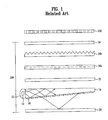
- FIG. 1 is a cross-sectional diagram of a liquid crystal display including an edge type backlight according to a related art.
- a liquid crystal display according to a related art mainly consists of a liquid crystal display panel 100 and a backlight 200.
- the backlight 200 in the drawing is an edge type backlight.
- the backlight 200 consists of a light guide plate 16, a lamp 14 provided to one side of the light guide plate 16, and a lamp housing 12 enclosing the lamp 14 to direct light irradiated from the lamp 14 toward the light guide plate 16 entirely.
- the light guide plate 16 plays a role in converting a linear light source to a surface light source so that the light irradiated from the lamp 14 can enter a front side of a liquid crystal display panel (not shown in the drawing). And, a multitude of dots 18 are provided to a bottom surface of the light guide plate 16.
- a reflector 20 is additionally provided under the light guide plate 16 to prevent light leakage.
- a diffusion plate 22, a pair of prism sheets 24a and 24b and a protective film 26 are sequentially provided over the light guide plate 16 to secure a viewing angle.
- a multitude of triangular linear prisms are provided to each of the prism sheets 24a and 24b. And, the linear prisms of the prism sheet 24a are arranged vertical to those of the other prism sheet 24b.
- the above-configured backlight of the related liquid crystal display needs many elements to be complicated, to have a thick volume and to cost much.
- the above-configured backlight of the related liquid crystal display needs the light guide plate to convert the linear light source to the surface light source, thereby having a considerable luminance difference.
- the present invention is directed to a liquid crystal display and fabricating method thereof that substantially obviate one or more problems due to limitations and disadvantages of the related art.
- An object of the present invention is to provide a liquid crystal display and fabricating method thereof, by which a backlight having a simple configuration, a reduced thickness and a low cost can be provided.
- Another object of the present invention is to provide a liquid crystal display and fabricating method thereof, by which a backlight having almost no luminance difference can be provided.
- a liquid crystal display according to the present invention includes a liquid crystal display panel having an upper substrate, a lower substrate and liquid crystals between the upper and lower substrates, an organic EL device provided under the lower substrate of the liquid crystal display panel to provide light to the liquid crystal display panel, and a cap boned to at least one of the lower substrate of the liquid crystal display panel and a substrate of the organic EL device to protect the organic EL device.
- the organic EL device includes a transparent substrate arranged under the lower substrate of the liquid crystal display panel, a first electrode formed on the transparent substrate, an organic EL layer formed on the first electrode, and a second electrode formed on the organic EL layer.
- the transparent substrate is formed of one selected from the group consisting of a polymer film, a multi-layer laminate film, an inorganic film, a multi-layer inorganic film and a multi-layer mixed film of laminate and inorganic films.
- the first electrode is formed of one selected from the group consisting of a transparent conductive material of ITO, an organic material, a metal, an inorganic material, a mixture of at least two of the transparent conductive material, the organic material, the metal and the inorganic material.
- the second electrode is formed of one selected from the group consisting of Mg-Ag, Al, a conductive metal layer, an alloy of at least two of the Mg-Ag, the Al and the conductive metal layer.
- the transparent substrate of the organic EL device and the lower substrate of the liquid crystal display panel are bonded to each other by an adhesive layer in-between.
- the liquid crystal display further includes a getter provided to a surface of the cap opposing the organic EL device to remove oxygen or moisture.
- the surface of the cap opposing the organic EL device is flat.
- the cap is bonded to the substrate of the organic EL device by a first adhesive agent and is bonded to a bottom of the lower substrate of the liquid crystal display panel by a second adhesive agent.
- the first and second adhesive agents are formed of a same material or different materials, respectively.
- each of the first and second adhesive agents includes one selected from the group consisting of a UV-hardening resin, a thermo-hardening resin and a mixture of the UV- and thermo-hardening resins.
- the cap includes a protrusion on a prescribed area of the surface opposing the organic EL device.
- the protrusion of the cap is bonded to the substrate of the organic EL device by a first adhesive agent and is bonded to a bottom of the lower substrate of the liquid crystal display panel by a second adhesive agent.
- the cap includes first and second protrusions on a prescribed area of the surface opposing the organic EL device.
- the first protrusion of the cap is bonded to the substrate of the organic EL device by a first adhesive agent and the second protrusion of the cap is bonded to a bottom of the lower substrate of the liquid crystal display panel by a second adhesive agent. More preferably, a height of the first protrusion of the cap is equal to or smaller than that of the second protrusion of the cap.
- a method of fabricating a liquid crystal display includes the steps of preparing a liquid crystal display panel having an upper substrate, a lower substrate and liquid crystals between the upper and lower substrates, preparing an organic EL device including a transparent substrate arranged under the lower substrate of the liquid crystal display panel, a first electrode formed on the transparent substrate, and an organic EL layer formed on the first electrode, primarily bonding a cap and the transparent substrate of the organic EL device so that the cap covers an upper part of the organic EL device, and secondarily bonding the cap primarily bonded to the transparent substrate of the organic EL device and the lower substrate of the liquid crystal display panel to each other.
- the step of primarily bonding the cap further includes the step of bonding the transparent substrate of the organic EL device and the lower substrate of the liquid crystal display panel.
- FIG. 1 is a cross-sectional diagram of a liquid crystal display including an edge type backlight according to a related art
- FIG. 2 is a cross-sectional diagram of a liquid crystal display according to the present invention.
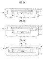
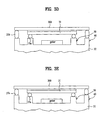
- FIGs. 3A to 3E are cross-sectional diagrams of various configurations of an organic EL device bonded to a cap of a liquid crystal display according to the present invention, respectively;
- FIG. 4 is a cross-sectional diagram of a cap of a liquid crystal display according to the present invention.
- FIGs. 5A to 5C are cross-sectional diagrams of a method of fabricating a liquid crystal display according to the present invention.
- FIG. 2 is a cross-sectional diagram of a liquid crystal display according to the present invention.
- a liquid crystal display according to the present invention includes a liquid crystal display panel 300 and a backlight 400 having an organic EL device 31 provided to a backside of the liquid crystal display panel 300 to directly illuminate the liquid crystal display 300 (direct type).
- the liquid crystal display panel 300 includes an upper substrate, a lower substrate and a liquid crystal layer.
- the organic EL device 31 is arranged under the lower substrate of the liquid crystal display panel 300 to provide light to the liquid crystal display panel 300.
- the organic EL device 31 includes a transparent substrate 31a arranged under the lower substrate of the liquid crystal display panel 300, a first electrode formed on the transparent substrate 31a, an organic EL layer formed on the first electrode 31b, and a second electrode 31d formed on the organic EL layer 31c.
- the transparent substrate 31a is formed of a polymer film, a multi-layer laminate film, an inorganic film, a multi-layer inorganic film, a multi-layer mixed film of laminate and inorganic films, or the like.
- the first electrode 31b is an anode formed of an transparent conductive material of ITO, an organic material, a metal, an inorganic material, a mixture of at least two of the former anode materials, or the like.
- the second electrode 31d is a cathode formed of Mg-Ag, Al, a conductive metal layer, an alloy of at least two of the former cathode materials, or the like.
- the transparent substrate 31a of the organic EL device 31 and the lower substrate of the liquid crystal display panel 300 can be bonded to each other by an adhesive layer 35.
- a cap 32 can be provided to at least one of the lower substrate of the liquid crystal display panel 300 and the transparent substrate of the organic EL device 31.
- a getter 34 which removes oxygen or moisture, can be provided to a surface of the cap 32 opposing the organic EL device 31.
- the cap 32 of the present invention can be bonded to the liquid crystal display panel 300 and the organic EL device 31 in various ways.
- FIGs. 3A to 3E are cross-sectional diagrams of various configurations of an organic EL device bonded to a cap of a liquid crystal display according to the present invention, respectively.
- a surface of a cap 32 opposing an organic EL device is flat.
- the cap 32 is bonded to the organic EL device by a first adhesive agent 33a and is bonded to a liquid crystal display panel 300 by a second adhesive agent 33b.
- first and second adhesive agents 33a and 33b may be the same material or may include different materials, respectively.
- Each of the first and second adhesive agents can be formed of a UV-hardening resin, a thermo-hardening resin, a mixture of them or the like.
- a cap 32 has a protrusion 40 on a prescribed area of a surface opposing an organic EL device 31.
- the protrusion 40 of the cap 32 is bonded to the organic EL device 31 by a first adhesive agent 33a and is bonded to a liquid crystal display panel 300 by a second adhesive agent 33b.
- a cap 32 has a protrusion 40 on an edge area of a surface opposing an organic EL device 31.
- a surface of the cap 32 having not protrusion is bonded to the organic EL device 31 by a first adhesive agent 33a and the protrusion.
- 40 is bonded to a liquid crystal display panel 300 by a second adhesive agent 33b.
- a cap 32 has first and second protrusions 50 and 60 on a prescribed area of a surface opposing an organic EL device 31.
- the first protrusion 50 of the cap 32 is bonded to the organic EL device 31 by a first adhesive agent 33a and the second protrusion 60 of the cap 32 is bonded to a liquid crystal display panel 300 by a second adhesive agent 33b.
- first and second protrusions 50 and 60 of the cap 32 in FIG. 3D are equal to each other in height, whereas the first protrusion 50 of the cap 32 in FIG. 3E is lower than that of the second protrusion 60 of the cap 32 in FIG. 3E.
- FIG. 4 is a cross-sectional diagram of a cap of a liquid crystal display according to the present invention.
- a cap 32 includes a first protrusion 50 and a second protrusion 60.
- a relation between the first and second protrusions 50 and 60 can be represented by a ⁇ b' and' c, d, e ⁇ 0' .
- FIGs. 5A to 5C are cross-sectional diagrams of a method of fabricating a liquid crystal display according to the present invention.
- a liquid crystal display panel including an upper substrate, a lower substrate and liquid crystals between the upper and lower substrates is prepared.
- the organic EL device 31 includes a transparent substrate 31a as an anode, a first electrode 31b, an organic EL layer 31c and a second electrode 31d as a cathode.
- a cap 32 and the organic EL device 31 are primarily bonded to each other by a first adhesive agent so that the cap 32 can cover an upper part of the organic EL device 31.
- the cap 32 primarily bonded to the organic EL device 31 is secondarily bonded to a liquid crystal display panel 300 by a second adhesive agent 33b.
- the lower substrate of the liquid crystal display panel 300 can be further bonded to the organic EL device 31 prior to the secondary bonding process.
- the present invention provides the following effects or advantages.
- the light source implemented with the organic EL device is used as the backlight of the liquid crystal display, whereby the backlight can be provided without the related art light guide plate, polarizing plates, prism sheets and the like.
- the present invention enables the fabrication of the liquid crystal display having a simple configuration, a reduced thickness, a low cost and almost no luminance difference.
- the expected device life span can be prevented from being reduced despite the substrate formed of the inorganic or polymer (laminate) material.
- the present invention enables the fabrication of the liquid crystal display having high efficiency and the long expected life span.
Landscapes
- Physics & Mathematics (AREA)
- Nonlinear Science (AREA)
- Mathematical Physics (AREA)
- Chemical & Material Sciences (AREA)
- Crystallography & Structural Chemistry (AREA)
- General Physics & Mathematics (AREA)
- Optics & Photonics (AREA)
- Electroluminescent Light Sources (AREA)
- Liquid Crystal (AREA)
- Devices For Indicating Variable Information By Combining Individual Elements (AREA)
Abstract
Description
- This application claims the benefit of the Korean Patent Application No. 10-2004-0055918, filed on July 19, 2004, which is hereby incorporated by reference as if fully set forth herein.
- The present invention relates to a liquid crystal display, and more particularly, to a liquid crystal display and fabricating method thereof. Although the present invention is suitable for a wide scope of applications, it is particularly suitable for a liquid crystal display having a backlight.
- Recently, as the information-oriented society is developing, the demands for flat panel displays advantageous in lightweight, slim size and low power consumption gradually rise.
- Among those flat panel displays, a liquid crystal display having excellent characteristics of resolution, color display, image quality and the like has been widely used for various fields of a TV monitor, a computer monitor and the like.
- Specifically, an active matrix LED (AM-LED) stands in the spotlight for a liquid crystal display having excellent resolution and moving picture implementation capability.
- A liquid crystal display generally consists of an upper substrate having a common electrode and a color filter, a lower substrate having a pixel electrode, and liquid crystals forming a liquid crystal layer provided between the upper and lower substrates.
- Since the liquid crystals fail in emitting light, the liquid crystal display needs a separate light source.
- The light source of the liquid crystal display is provided to a backside of a liquid crystal display panel and is called a backlight. And, the backlight is classified into a direct type and an edge type.
- In the direct type, a backlight is placed under a liquid crystal display panel to illuminate a front side of the liquid crystal display panel. In the edge type, a backlight is provided to one side or both sides of a liquid crystal display panel to diffuse light in a manner that a light guide plate, a reflector and the like reflect the light.
- And, the edge type backlight, of which volume can be reduced, is mainly used.
- A liquid crystal display according to a related art is explained with reference to the attached drawing as follows.
- FIG. 1 is a cross-sectional diagram of a liquid crystal display including an edge type backlight according to a related art.
- Referring to FIG. 1, a liquid crystal display according to a related art mainly consists of a liquid
crystal display panel 100 and abacklight 200. - The
backlight 200 in the drawing is an edge type backlight. And, thebacklight 200 consists of alight guide plate 16, alamp 14 provided to one side of thelight guide plate 16, and alamp housing 12 enclosing thelamp 14 to direct light irradiated from thelamp 14 toward thelight guide plate 16 entirely. - In this case, the
light guide plate 16 plays a role in converting a linear light source to a surface light source so that the light irradiated from thelamp 14 can enter a front side of a liquid crystal display panel (not shown in the drawing). And, a multitude ofdots 18 are provided to a bottom surface of thelight guide plate 16. - A
reflector 20 is additionally provided under thelight guide plate 16 to prevent light leakage. - A diffusion plate 22, a pair of
prism sheets 24a and 24b and aprotective film 26 are sequentially provided over thelight guide plate 16 to secure a viewing angle. - A multitude of triangular linear prisms are provided to each of the
prism sheets 24a and 24b. And, the linear prisms of theprism sheet 24a are arranged vertical to those of the other prism sheet 24b. - However, the above-configured backlight of the related liquid crystal display needs many elements to be complicated, to have a thick volume and to cost much.
- Moreover, the above-configured backlight of the related liquid crystal display needs the light guide plate to convert the linear light source to the surface light source, thereby having a considerable luminance difference.
- Accordingly, the present invention is directed to a liquid crystal display and fabricating method thereof that substantially obviate one or more problems due to limitations and disadvantages of the related art.
- An object of the present invention is to provide a liquid crystal display and fabricating method thereof, by which a backlight having a simple configuration, a reduced thickness and a low cost can be provided.
- Another object of the present invention is to provide a liquid crystal display and fabricating method thereof, by which a backlight having almost no luminance difference can be provided.
- Additional advantages, objects, and features of the invention will be set forth in part in the description which follows and in part will become apparent to those having ordinary skill in the art upon examination of the following or may be learned from practice of the invention. The objectives and other advantages of the invention may be realized and attained by the structure particularly pointed out in the written description and claims hereof as well as the appended drawings.
- To achieve these objects and other advantages and in accordance with the purpose of the invention, as embodied and broadly described herein, a liquid crystal display according to the present invention includes a liquid crystal display panel having an upper substrate, a lower substrate and liquid crystals between the upper and lower substrates, an organic EL device provided under the lower substrate of the liquid crystal display panel to provide light to the liquid crystal display panel, and a cap boned to at least one of the lower substrate of the liquid crystal display panel and a substrate of the organic EL device to protect the organic EL device.
- Preferably, the organic EL device includes a transparent substrate arranged under the lower substrate of the liquid crystal display panel, a first electrode formed on the transparent substrate, an organic EL layer formed on the first electrode, and a second electrode formed on the organic EL layer.
- More preferably, the transparent substrate is formed of one selected from the group consisting of a polymer film, a multi-layer laminate film, an inorganic film, a multi-layer inorganic film and a multi-layer mixed film of laminate and inorganic films. More preferably, the first electrode is formed of one selected from the group consisting of a transparent conductive material of ITO, an organic material, a metal, an inorganic material, a mixture of at least two of the transparent conductive material, the organic material, the metal and the inorganic material. More preferably, the second electrode is formed of one selected from the group consisting of Mg-Ag, Al, a conductive metal layer, an alloy of at least two of the Mg-Ag, the Al and the conductive metal layer.
- More preferably, the transparent substrate of the organic EL device and the lower substrate of the liquid crystal display panel are bonded to each other by an adhesive layer in-between.
- Preferably, the liquid crystal display further includes a getter provided to a surface of the cap opposing the organic EL device to remove oxygen or moisture.
- Preferably, the surface of the cap opposing the organic EL device is flat.
- More preferably, the cap is bonded to the substrate of the organic EL device by a first adhesive agent and is bonded to a bottom of the lower substrate of the liquid crystal display panel by a second adhesive agent. More preferably, the first and second adhesive agents are formed of a same material or different materials, respectively. More preferably, each of the first and second adhesive agents includes one selected from the group consisting of a UV-hardening resin, a thermo-hardening resin and a mixture of the UV- and thermo-hardening resins.
- Preferably, the cap includes a protrusion on a prescribed area of the surface opposing the organic EL device.
- More preferably, the protrusion of the cap is bonded to the substrate of the organic EL device by a first adhesive agent and is bonded to a bottom of the lower substrate of the liquid crystal display panel by a second adhesive agent.
- Preferably, the cap includes first and second protrusions on a prescribed area of the surface opposing the organic EL device.
- More preferably, the first protrusion of the cap is bonded to the substrate of the organic EL device by a first adhesive agent and the second protrusion of the cap is bonded to a bottom of the lower substrate of the liquid crystal display panel by a second adhesive agent. More preferably, a height of the first protrusion of the cap is equal to or smaller than that of the second protrusion of the cap.
- In another aspect of the present invention, a method of fabricating a liquid crystal display includes the steps of preparing a liquid crystal display panel having an upper substrate, a lower substrate and liquid crystals between the upper and lower substrates, preparing an organic EL device including a transparent substrate arranged under the lower substrate of the liquid crystal display panel, a first electrode formed on the transparent substrate, and an organic EL layer formed on the first electrode, primarily bonding a cap and the transparent substrate of the organic EL device so that the cap covers an upper part of the organic EL device, and secondarily bonding the cap primarily bonded to the transparent substrate of the organic EL device and the lower substrate of the liquid crystal display panel to each other.
- Preferably, the step of primarily bonding the cap further includes the step of bonding the transparent substrate of the organic EL device and the lower substrate of the liquid crystal display panel.
- It is to be understood that both the foregoing general description and the following detailed description of the present invention are exemplary and explanatory and are intended to provide further explanation of the invention as claimed.
- The accompanying drawings, which are included to provide a further understanding of the invention and are incorporated in and constitute a part of this application, illustrate embodiment(s) of the invention and together with the description serve to explain the principle of the invention. In the drawings:
- FIG. 1 is a cross-sectional diagram of a liquid crystal display including an edge type backlight according to a related art;
- FIG. 2 is a cross-sectional diagram of a liquid crystal display according to the present invention;
- FIGs. 3A to 3E are cross-sectional diagrams of various configurations of an organic EL device bonded to a cap of a liquid crystal display according to the present invention, respectively;
- FIG. 4 is a cross-sectional diagram of a cap of a liquid crystal display according to the present invention; and
- FIGs. 5A to 5C are cross-sectional diagrams of a method of fabricating a liquid crystal display according to the present invention.
- Reference will now be made in detail to the preferred embodiments of the present invention, examples of which are illustrated in the accompanying drawings. Wherever possible, the same reference numbers will be used throughout the drawings to refer to the same or like parts.
- FIG. 2 is a cross-sectional diagram of a liquid crystal display according to the present invention.
- Referring to FIG. 2, a liquid crystal display according to the present invention includes a liquid
crystal display panel 300 and abacklight 400 having anorganic EL device 31 provided to a backside of the liquidcrystal display panel 300 to directly illuminate the liquid crystal display 300 (direct type). - In this case, the liquid
crystal display panel 300 includes an upper substrate, a lower substrate and a liquid crystal layer. - And, the
organic EL device 31 is arranged under the lower substrate of the liquidcrystal display panel 300 to provide light to the liquidcrystal display panel 300. - Moreover, the
organic EL device 31 includes atransparent substrate 31a arranged under the lower substrate of the liquidcrystal display panel 300, a first electrode formed on thetransparent substrate 31a, an organic EL layer formed on thefirst electrode 31b, and asecond electrode 31d formed on theorganic EL layer 31c. - In this case, the
transparent substrate 31a is formed of a polymer film, a multi-layer laminate film, an inorganic film, a multi-layer inorganic film, a multi-layer mixed film of laminate and inorganic films, or the like. - The
first electrode 31b is an anode formed of an transparent conductive material of ITO, an organic material, a metal, an inorganic material, a mixture of at least two of the former anode materials, or the like. - The
second electrode 31d is a cathode formed of Mg-Ag, Al, a conductive metal layer, an alloy of at least two of the former cathode materials, or the like. - The
transparent substrate 31a of theorganic EL device 31 and the lower substrate of the liquidcrystal display panel 300 can be bonded to each other by anadhesive layer 35. - To prevent an expected life span of the
organic EL device 31 from being shortened by moisture permeation, acap 32 can be provided to at least one of the lower substrate of the liquidcrystal display panel 300 and the transparent substrate of theorganic EL device 31. - A
getter 34, which removes oxygen or moisture, can be provided to a surface of thecap 32 opposing theorganic EL device 31. - And, the
cap 32 of the present invention can be bonded to the liquidcrystal display panel 300 and theorganic EL device 31 in various ways. - FIGs. 3A to 3E are cross-sectional diagrams of various configurations of an organic EL device bonded to a cap of a liquid crystal display according to the present invention, respectively.
- Referring to FIG. 3A, a surface of a
cap 32 opposing an organic EL device is flat. Thecap 32 is bonded to the organic EL device by a firstadhesive agent 33a and is bonded to a liquidcrystal display panel 300 by a secondadhesive agent 33b. - In this case, the first and second
adhesive agents - Referring to FIG. 3B, a
cap 32 has aprotrusion 40 on a prescribed area of a surface opposing anorganic EL device 31. Theprotrusion 40 of thecap 32 is bonded to theorganic EL device 31 by a firstadhesive agent 33a and is bonded to a liquidcrystal display panel 300 by a secondadhesive agent 33b. - Referring to FIG. 3C, a
cap 32 has aprotrusion 40 on an edge area of a surface opposing anorganic EL device 31. A surface of thecap 32 having not protrusion is bonded to theorganic EL device 31 by a firstadhesive agent 33a and the protrusion. 40 is bonded to a liquidcrystal display panel 300 by a secondadhesive agent 33b. - Referring to FIG. 3D and 3E, a
cap 32 has first andsecond protrusions organic EL device 31. Thefirst protrusion 50 of thecap 32 is bonded to theorganic EL device 31 by a firstadhesive agent 33a and thesecond protrusion 60 of thecap 32 is bonded to a liquidcrystal display panel 300 by a secondadhesive agent 33b. - In particular, the first and
second protrusions cap 32 in FIG. 3D are equal to each other in height, whereas thefirst protrusion 50 of thecap 32 in FIG. 3E is lower than that of thesecond protrusion 60 of thecap 32 in FIG. 3E. - FIG. 4 is a cross-sectional diagram of a cap of a liquid crystal display according to the present invention.
- Referring to FIG. 4, a
cap 32 includes afirst protrusion 50 and asecond protrusion 60. - A relation between the first and
second protrusions - A method of fabricating the above-configured liquid crystal display is explained with reference to the attached drawings as follows.
- FIGs. 5A to 5C are cross-sectional diagrams of a method of fabricating a liquid crystal display according to the present invention.
- Referring to FIG. 5A, first of all, a liquid crystal display panel including an upper substrate, a lower substrate and liquid crystals between the upper and lower substrates is prepared.
- And, an
organic EL device 31 is prepared. In this case, theorganic EL device 31 includes atransparent substrate 31a as an anode, afirst electrode 31b, anorganic EL layer 31c and asecond electrode 31d as a cathode. - Referring to FIG. 5B, a
cap 32 and theorganic EL device 31 are primarily bonded to each other by a first adhesive agent so that thecap 32 can cover an upper part of theorganic EL device 31. - Referring to FIG. 5C, the
cap 32 primarily bonded to theorganic EL device 31 is secondarily bonded to a liquidcrystal display panel 300 by a secondadhesive agent 33b. - Optionally, the lower substrate of the liquid
crystal display panel 300 can be further bonded to theorganic EL device 31 prior to the secondary bonding process. - Accordingly, the present invention provides the following effects or advantages.
- First of all, the light source implemented with the organic EL device is used as the backlight of the liquid crystal display, whereby the backlight can be provided without the related art light guide plate, polarizing plates, prism sheets and the like.
- Therefore, the present invention enables the fabrication of the liquid crystal display having a simple configuration, a reduced thickness, a low cost and almost no luminance difference.
- Secondly, by cutting off the moisture permeation in a manner of the double-bonding of the organic EL device, the expected device life span can be prevented from being reduced despite the substrate formed of the inorganic or polymer (laminate) material.
- Therefore, the present invention enables the fabrication of the liquid crystal display having high efficiency and the long expected life span.
- It will be apparent to those skilled in the art that various modifications and variations can be made in the present invention without departing from the spirit or scope of the inventions. Thus, it is intended that the present invention covers the modifications and variations of this invention provided they come within the scope of the appended claims and their equivalents.
Claims (18)
- A liquid crystal display comprising:a liquid crystal display panel having an upper substrate, a lower substrate and liquid crystals between the upper and lower substrates;an organic EL device provided under the lower substrate of the liquid crystal display panel to provide light to the liquid crystal display panel; anda cap boned to at least one of the lower substrate of the liquid crystal display panel and a substrate of the organic EL device to protect the organic EL device.
- The liquid crystal display of claim 1, the organic EL device comprising:a transparent substrate arranged under the lower substrate of the liquid crystal display panel;a first electrode formed on the transparent substrate; an organic EL layer formed on the first electrode; anda second electrode formed on the organic EL layer.
- The liquid crystal display of claim 2, wherein the transparent substrate is formed of one selected from the group consisting of a polymer film, a multi-layer laminate film, an inorganic film, a multi-layer inorganic film and a multi-layer mixed film of laminate and inorganic films.
- The liquid crystal display of claim 2, wherein the first electrode is formed of one selected from the group consisting of a transparent conductive material of ITO, an organic material, a metal, an inorganic material, a mixture of at least two of the transparent conductive material, the organic material, the metal and the inorganic material.
- The liquid crystal display of claim 2, wherein the second electrode is formed of one selected from the group consisting of Mg-Ag, A1, a conductive metal layer, an alloy of at least two of the Mg-Ag, the A1 and the conductive metal layer.
- The liquid crystal display of claim 2, wherein the transparent substrate of the organic EL device and the lower substrate of the liquid crystal display panel are bonded to each other by an adhesive layer in-between.
- The liquid crystal display of claim 1, further comprising a getter provided to a surface of the cap opposing the organic EL device to remove oxygen or moisture.
- The liquid crystal display of claim 1, wherein the surface of the cap opposing the organic EL device is flat.
- The liquid crystal display of claim 8, wherein the cap is bonded to the substrate of the organic EL device by a first adhesive agent and is bonded to a bottom of the lower substrate of the liquid crystal display panel by a second adhesive agent.
- The liquid crystal display of claim 9, wherein the first and second adhesive agents are formed of a same material or different materials, respectively.
- The liquid crystal display of claim 9, wherein each of the first and second adhesive agents comprises one selected from the group consisting of a UV-hardening resin, a thermo-hardening resin and a mixture of the UV- and thermo-hardening resins.
- The liquid crystal display of claim 1, wherein the cap comprises a protrusion on a prescribed area of the surface opposing the organic EL device.
- The liquid crystal display of claim 12, wherein the protrusion of the cap is bonded to the substrate of the organic EL device by a first adhesive agent and is bonded to a bottom of the lower substrate of the liquid crystal display panel by a second adhesive agent.
- The liquid crystal display of claim 1, wherein the cap comprises first and second protrusions on a prescribed. area of the surface opposing the organic EL device.
- The liquid crystal display of claim 14, wherein the first protrusion of the cap is bonded to the substrate of the organic EL device by a first adhesive agent and wherein the second protrusion of the cap is bonded to a bottom of the lower substrate of the liquid crystal display panel by a second adhesive agent.
- The liquid crystal display of claim 14, wherein a height of the first protrusion of the cap is equal to or smaller than that of the second protrusion of the cap.
- A method of fabricating a liquid crystal display, comprising the steps of:preparing a liquid crystal display panel having an upper substrate, a lower substrate and liquid crystals between the upper and lower substrates;preparing an organic EL device including a transparent substrate arranged under the lower substrate of the liquid crystal display panel, a first electrode formed on the transparent substrate, and an organic EL layer formed on the first electrode;primarily bonding a cap and the transparent substrate of the organic EL device so that the cap covers an upper part of the organic EL device; andsecondarily bonding the cap primarily bonded to the transparent substrate of the organic EL device and the lower substrate of the liquid crystal display panel to each other.
- The method of claim 17, the step of primarily bonding the cap, further comprising the step of bonding the transparent substrate of the organic EL device and the lower substrate of the liquid crystal display panel.
Applications Claiming Priority (1)
| Application Number | Priority Date | Filing Date | Title |
|---|---|---|---|
| KR1020040055918A KR20060007161A (en) | 2004-07-19 | 2004-07-19 | LCD Display |
Publications (2)
| Publication Number | Publication Date |
|---|---|
| EP1619544A1 true EP1619544A1 (en) | 2006-01-25 |
| EP1619544B1 EP1619544B1 (en) | 2007-09-26 |
Family
ID=35079435
Family Applications (1)
| Application Number | Title | Priority Date | Filing Date |
|---|---|---|---|
| EP05015538A Expired - Lifetime EP1619544B1 (en) | 2004-07-19 | 2005-07-18 | Liquid crystal display and fabricating method thereof |
Country Status (7)
| Country | Link |
|---|---|
| US (1) | US7675585B2 (en) |
| EP (1) | EP1619544B1 (en) |
| JP (1) | JP4395773B2 (en) |
| KR (1) | KR20060007161A (en) |
| CN (1) | CN100410741C (en) |
| AT (1) | ATE374386T1 (en) |
| DE (1) | DE602005002594T2 (en) |
Families Citing this family (6)
| Publication number | Priority date | Publication date | Assignee | Title |
|---|---|---|---|---|
| TWI326372B (en) * | 2005-08-08 | 2010-06-21 | Ind Tech Res Inst | Emireflective display and method thereof |
| US7791115B2 (en) * | 2005-11-29 | 2010-09-07 | Samsung Mobile Display Co., Ltd. | Organic light emitting display device |
| KR101342652B1 (en) * | 2006-11-15 | 2013-12-16 | 삼성디스플레이 주식회사 | liquid crystal display |
| US9070900B2 (en) * | 2008-11-13 | 2015-06-30 | Joled Inc | Method of manufacturing display, and display |
| JP5892736B2 (en) * | 2011-05-24 | 2016-03-23 | ソニー株式会社 | Display device |
| CN103091898B (en) * | 2013-02-06 | 2015-12-02 | 京东方科技集团股份有限公司 | LCDs and preparation method thereof, display device |
Citations (5)
| Publication number | Priority date | Publication date | Assignee | Title |
|---|---|---|---|---|
| EP0500382A2 (en) * | 1991-02-21 | 1992-08-26 | Sharp Kabushiki Kaisha | Moisture proof thin film electroluminescent panel |
| JPH0963766A (en) * | 1995-08-29 | 1997-03-07 | Sharp Corp | Thin film EL panel |
| JP2002098956A (en) * | 2000-09-26 | 2002-04-05 | Seiko Epson Corp | Liquid crystal device and electronic device |
| KR100366526B1 (en) * | 1999-09-29 | 2002-12-31 | 산요 덴키 가부시키가이샤 | Sealing structure of electro luminescence device |
| US20030102801A1 (en) * | 2001-11-09 | 2003-06-05 | Shigeru Senbonmatsu | Lighting device with a reflecting layer and liquid crystal display device |
Family Cites Families (22)
| Publication number | Priority date | Publication date | Assignee | Title |
|---|---|---|---|---|
| JPH0320317A (en) | 1989-03-14 | 1991-01-29 | Mitsui Toatsu Chem Inc | Production of fine amino resin particle having narrow particle diameter distribution |
| JPH09148066A (en) * | 1995-11-24 | 1997-06-06 | Pioneer Electron Corp | Organic electroluminescent element |
| JPH10125463A (en) | 1995-12-28 | 1998-05-15 | Matsushita Electric Ind Co Ltd | Organic electroluminescence element, liquid crystal lighting device, display device, and method of manufacturing organic electroluminescence element |
| JP2000241811A (en) | 1999-02-22 | 2000-09-08 | Toyota Motor Corp | Field sequential liquid crystal display |
| JP2001068271A (en) * | 1999-08-24 | 2001-03-16 | Fuji Photo Film Co Ltd | Light emitting element |
| JP2001102167A (en) * | 1999-09-29 | 2001-04-13 | Sanyo Electric Co Ltd | Electroluminescence display device |
| TWI228616B (en) * | 1999-11-30 | 2005-03-01 | Samsung Electronics Co Ltd | Liquid crystal display device |
| JP3409764B2 (en) * | 1999-12-28 | 2003-05-26 | 日本電気株式会社 | Manufacturing method of organic EL display panel |
| JP2002072207A (en) * | 2000-09-04 | 2002-03-12 | Seiko Epson Corp | Liquid crystal display |
| JP4711273B2 (en) | 2000-11-20 | 2011-06-29 | スタンレー電気株式会社 | Illuminated liquid crystal display device |
| JP2002163914A (en) * | 2000-11-24 | 2002-06-07 | Nec Corp | Illumination device, liquid crystal display device using the illumination device, and method of manufacturing the same |
| KR100623224B1 (en) * | 2000-11-27 | 2006-09-11 | 삼성에스디아이 주식회사 | Backlight of LCD and Manufacturing Method Thereof |
| JP2002329576A (en) * | 2001-04-27 | 2002-11-15 | Semiconductor Energy Lab Co Ltd | Light emitting device and manufacturing method thereof |
| KR100435203B1 (en) * | 2001-08-17 | 2004-06-09 | 주식회사 진우엔지니어링 | White light-emitting organic electroluminescent device for back light and liquid crystal display device using itself |
| KR100793729B1 (en) * | 2001-09-27 | 2008-01-10 | 삼성전자주식회사 | LCD Display |
| JP3975779B2 (en) * | 2002-03-01 | 2007-09-12 | 株式会社日立製作所 | Organic electroluminescence device and manufacturing method thereof |
| JP3864851B2 (en) * | 2002-06-03 | 2007-01-10 | 株式会社豊田自動織機 | Planar light emitting device |
| JP4118099B2 (en) * | 2002-07-22 | 2008-07-16 | 三洋電機株式会社 | Electroluminescence display device |
| KR100474001B1 (en) * | 2002-08-14 | 2005-03-10 | 엘지.필립스 엘시디 주식회사 | Dual Panel Type Organic Electroluminescent Device and Method for Fabricating the same |
| TW556447B (en) * | 2002-09-05 | 2003-10-01 | Au Optronics Corp | An organic light emitting diode |
| JP4255302B2 (en) * | 2003-03-31 | 2009-04-15 | シャープ株式会社 | LIQUID CRYSTAL DISPLAY LIGHTING DEVICE AND LIQUID CRYSTAL DISPLAY DEVICE |
| JP4225237B2 (en) * | 2004-04-21 | 2009-02-18 | セイコーエプソン株式会社 | ORGANIC EL DEVICE, METHOD FOR MANUFACTURING ORGANIC EL DEVICE, AND ELECTRONIC DEVICE |
-
2004
- 2004-07-19 KR KR1020040055918A patent/KR20060007161A/en not_active Ceased
-
2005
- 2005-07-18 US US11/182,770 patent/US7675585B2/en not_active Expired - Fee Related
- 2005-07-18 AT AT05015538T patent/ATE374386T1/en not_active IP Right Cessation
- 2005-07-18 EP EP05015538A patent/EP1619544B1/en not_active Expired - Lifetime
- 2005-07-18 DE DE602005002594T patent/DE602005002594T2/en not_active Expired - Lifetime
- 2005-07-19 CN CNB2005100852623A patent/CN100410741C/en not_active Expired - Fee Related
- 2005-07-19 JP JP2005208405A patent/JP4395773B2/en not_active Expired - Fee Related
Patent Citations (6)
| Publication number | Priority date | Publication date | Assignee | Title |
|---|---|---|---|---|
| EP0500382A2 (en) * | 1991-02-21 | 1992-08-26 | Sharp Kabushiki Kaisha | Moisture proof thin film electroluminescent panel |
| JPH0963766A (en) * | 1995-08-29 | 1997-03-07 | Sharp Corp | Thin film EL panel |
| KR100366526B1 (en) * | 1999-09-29 | 2002-12-31 | 산요 덴키 가부시키가이샤 | Sealing structure of electro luminescence device |
| US6833668B1 (en) * | 1999-09-29 | 2004-12-21 | Sanyo Electric Co., Ltd. | Electroluminescence display device having a desiccant |
| JP2002098956A (en) * | 2000-09-26 | 2002-04-05 | Seiko Epson Corp | Liquid crystal device and electronic device |
| US20030102801A1 (en) * | 2001-11-09 | 2003-06-05 | Shigeru Senbonmatsu | Lighting device with a reflecting layer and liquid crystal display device |
Non-Patent Citations (2)
| Title |
|---|
| PATENT ABSTRACTS OF JAPAN vol. 1997, no. 07 31 July 1997 (1997-07-31) * |
| PATENT ABSTRACTS OF JAPAN vol. 2002, no. 08 5 August 2002 (2002-08-05) * |
Also Published As
| Publication number | Publication date |
|---|---|
| DE602005002594T2 (en) | 2008-01-24 |
| JP4395773B2 (en) | 2010-01-13 |
| JP2006031021A (en) | 2006-02-02 |
| CN100410741C (en) | 2008-08-13 |
| CN1725071A (en) | 2006-01-25 |
| DE602005002594D1 (en) | 2007-11-08 |
| US20060012732A1 (en) | 2006-01-19 |
| KR20060007161A (en) | 2006-01-24 |
| EP1619544B1 (en) | 2007-09-26 |
| ATE374386T1 (en) | 2007-10-15 |
| US7675585B2 (en) | 2010-03-09 |
Similar Documents
| Publication | Publication Date | Title |
|---|---|---|
| CN108333822B (en) | Liquid crystal display device having a plurality of pixel electrodes | |
| US8432525B2 (en) | Backlight unit and liquid crystal display device having the same | |
| US9063267B2 (en) | Liquid crystal display device | |
| JP4679985B2 (en) | Liquid crystal display device | |
| US20130242229A1 (en) | Reflective plate and method for manufacturing the same and backlight unit for liquid crystal display device using the same | |
| US20080055518A1 (en) | Light weight liquid crystal display | |
| KR101737116B1 (en) | Liquid crystal display device | |
| US20110085123A1 (en) | Display device and portable display apparatus including the same | |
| KR101633125B1 (en) | Display device | |
| US8189137B2 (en) | Backlight unit and liquid crystal display device having the same | |
| EP1619544B1 (en) | Liquid crystal display and fabricating method thereof | |
| US20060109395A1 (en) | Area light source device and liquid crystal display device including the same | |
| US7471354B2 (en) | Backlight module and liquid crystal display | |
| KR20140062644A (en) | Fluorescent substance film, backlight unit and display device comprising the same | |
| US20080088773A1 (en) | Backlight module with polarizer film, liquid crystal display using same, and method for assembling liquid crystal display | |
| KR101749750B1 (en) | Backlight Unit And Liquid Crystal Diplay | |
| KR101753910B1 (en) | Liquid crystal display device | |
| KR20130072792A (en) | Backlight unit and liquid crystal display device having the same | |
| JP4717406B2 (en) | How to store the display panel | |
| KR100672416B1 (en) | LCD Display | |
| KR101782644B1 (en) | Led assembly, backlight uint and liquid crystal display comprising of the same | |
| JP2006171378A (en) | Liquid crystal display | |
| KR101702130B1 (en) | Liquid crystal display device and method assembling the same | |
| KR20120075863A (en) | Liquid crystal display device | |
| KR101946062B1 (en) | Liquid crystall display device |
Legal Events
| Date | Code | Title | Description |
|---|---|---|---|
| PUAI | Public reference made under article 153(3) epc to a published international application that has entered the european phase |
Free format text: ORIGINAL CODE: 0009012 |
|
| 17P | Request for examination filed |
Effective date: 20050718 |
|
| AK | Designated contracting states |
Kind code of ref document: A1 Designated state(s): AT BE BG CH CY CZ DE DK EE ES FI FR GB GR HU IE IS IT LI LT LU LV MC NL PL PT RO SE SI SK TR |
|
| AX | Request for extension of the european patent |
Extension state: AL BA HR MK YU |
|
| 17Q | First examination report despatched |
Effective date: 20060628 |
|
| AKX | Designation fees paid |
Designated state(s): AT BE BG CH CY CZ DE DK EE ES FI FR GB GR HU IE IS IT LI LT LU LV MC NL PL PT RO SE SI SK TR |
|
| 17Q | First examination report despatched |
Effective date: 20060628 |
|
| GRAP | Despatch of communication of intention to grant a patent |
Free format text: ORIGINAL CODE: EPIDOSNIGR1 |
|
| GRAS | Grant fee paid |
Free format text: ORIGINAL CODE: EPIDOSNIGR3 |
|
| GRAA | (expected) grant |
Free format text: ORIGINAL CODE: 0009210 |
|
| AK | Designated contracting states |
Kind code of ref document: B1 Designated state(s): AT BE BG CH CY CZ DE DK EE ES FI FR GB GR HU IE IS IT LI LT LU LV MC NL PL PT RO SE SI SK TR |
|
| REG | Reference to a national code |
Ref country code: GB Ref legal event code: FG4D |
|
| REG | Reference to a national code |
Ref country code: CH Ref legal event code: EP |
|
| REF | Corresponds to: |
Ref document number: 602005002594 Country of ref document: DE Date of ref document: 20071108 Kind code of ref document: P |
|
| REG | Reference to a national code |
Ref country code: IE Ref legal event code: FG4D |
|
| PG25 | Lapsed in a contracting state [announced via postgrant information from national office to epo] |
Ref country code: FI Free format text: LAPSE BECAUSE OF FAILURE TO SUBMIT A TRANSLATION OF THE DESCRIPTION OR TO PAY THE FEE WITHIN THE PRESCRIBED TIME-LIMIT Effective date: 20070926 Ref country code: LT Free format text: LAPSE BECAUSE OF FAILURE TO SUBMIT A TRANSLATION OF THE DESCRIPTION OR TO PAY THE FEE WITHIN THE PRESCRIBED TIME-LIMIT Effective date: 20070926 |
|
| PG25 | Lapsed in a contracting state [announced via postgrant information from national office to epo] |
Ref country code: PL Free format text: LAPSE BECAUSE OF FAILURE TO SUBMIT A TRANSLATION OF THE DESCRIPTION OR TO PAY THE FEE WITHIN THE PRESCRIBED TIME-LIMIT Effective date: 20070926 Ref country code: AT Free format text: LAPSE BECAUSE OF FAILURE TO SUBMIT A TRANSLATION OF THE DESCRIPTION OR TO PAY THE FEE WITHIN THE PRESCRIBED TIME-LIMIT Effective date: 20070926 |
|
| NLV1 | Nl: lapsed or annulled due to failure to fulfill the requirements of art. 29p and 29m of the patents act | ||
| PG25 | Lapsed in a contracting state [announced via postgrant information from national office to epo] |
Ref country code: BE Free format text: LAPSE BECAUSE OF FAILURE TO SUBMIT A TRANSLATION OF THE DESCRIPTION OR TO PAY THE FEE WITHIN THE PRESCRIBED TIME-LIMIT Effective date: 20070926 Ref country code: LV Free format text: LAPSE BECAUSE OF FAILURE TO SUBMIT A TRANSLATION OF THE DESCRIPTION OR TO PAY THE FEE WITHIN THE PRESCRIBED TIME-LIMIT Effective date: 20070926 |
|
| REG | Reference to a national code |
Ref country code: CH Ref legal event code: PL |
|
| ET | Fr: translation filed | ||
| PG25 | Lapsed in a contracting state [announced via postgrant information from national office to epo] |
Ref country code: NL Free format text: LAPSE BECAUSE OF FAILURE TO SUBMIT A TRANSLATION OF THE DESCRIPTION OR TO PAY THE FEE WITHIN THE PRESCRIBED TIME-LIMIT Effective date: 20070926 Ref country code: LI Free format text: LAPSE BECAUSE OF FAILURE TO SUBMIT A TRANSLATION OF THE DESCRIPTION OR TO PAY THE FEE WITHIN THE PRESCRIBED TIME-LIMIT Effective date: 20070926 Ref country code: GR Free format text: LAPSE BECAUSE OF FAILURE TO SUBMIT A TRANSLATION OF THE DESCRIPTION OR TO PAY THE FEE WITHIN THE PRESCRIBED TIME-LIMIT Effective date: 20071227 Ref country code: CH Free format text: LAPSE BECAUSE OF FAILURE TO SUBMIT A TRANSLATION OF THE DESCRIPTION OR TO PAY THE FEE WITHIN THE PRESCRIBED TIME-LIMIT Effective date: 20070926 Ref country code: ES Free format text: LAPSE BECAUSE OF FAILURE TO SUBMIT A TRANSLATION OF THE DESCRIPTION OR TO PAY THE FEE WITHIN THE PRESCRIBED TIME-LIMIT Effective date: 20080106 |
|
| PG25 | Lapsed in a contracting state [announced via postgrant information from national office to epo] |
Ref country code: SK Free format text: LAPSE BECAUSE OF FAILURE TO SUBMIT A TRANSLATION OF THE DESCRIPTION OR TO PAY THE FEE WITHIN THE PRESCRIBED TIME-LIMIT Effective date: 20070926 Ref country code: CZ Free format text: LAPSE BECAUSE OF FAILURE TO SUBMIT A TRANSLATION OF THE DESCRIPTION OR TO PAY THE FEE WITHIN THE PRESCRIBED TIME-LIMIT Effective date: 20070926 Ref country code: IS Free format text: LAPSE BECAUSE OF FAILURE TO SUBMIT A TRANSLATION OF THE DESCRIPTION OR TO PAY THE FEE WITHIN THE PRESCRIBED TIME-LIMIT Effective date: 20080126 Ref country code: PT Free format text: LAPSE BECAUSE OF FAILURE TO SUBMIT A TRANSLATION OF THE DESCRIPTION OR TO PAY THE FEE WITHIN THE PRESCRIBED TIME-LIMIT Effective date: 20080226 |
|
| PG25 | Lapsed in a contracting state [announced via postgrant information from national office to epo] |
Ref country code: RO Free format text: LAPSE BECAUSE OF FAILURE TO SUBMIT A TRANSLATION OF THE DESCRIPTION OR TO PAY THE FEE WITHIN THE PRESCRIBED TIME-LIMIT Effective date: 20070926 Ref country code: SE Free format text: LAPSE BECAUSE OF FAILURE TO SUBMIT A TRANSLATION OF THE DESCRIPTION OR TO PAY THE FEE WITHIN THE PRESCRIBED TIME-LIMIT Effective date: 20071226 |
|
| PG25 | Lapsed in a contracting state [announced via postgrant information from national office to epo] |
Ref country code: DK Free format text: LAPSE BECAUSE OF FAILURE TO SUBMIT A TRANSLATION OF THE DESCRIPTION OR TO PAY THE FEE WITHIN THE PRESCRIBED TIME-LIMIT Effective date: 20070926 |
|
| PLBE | No opposition filed within time limit |
Free format text: ORIGINAL CODE: 0009261 |
|
| STAA | Information on the status of an ep patent application or granted ep patent |
Free format text: STATUS: NO OPPOSITION FILED WITHIN TIME LIMIT |
|
| 26N | No opposition filed |
Effective date: 20080627 |
|
| PG25 | Lapsed in a contracting state [announced via postgrant information from national office to epo] |
Ref country code: MC Free format text: LAPSE BECAUSE OF NON-PAYMENT OF DUE FEES Effective date: 20080731 |
|
| PG25 | Lapsed in a contracting state [announced via postgrant information from national office to epo] |
Ref country code: EE Free format text: LAPSE BECAUSE OF FAILURE TO SUBMIT A TRANSLATION OF THE DESCRIPTION OR TO PAY THE FEE WITHIN THE PRESCRIBED TIME-LIMIT Effective date: 20070926 |
|
| PG25 | Lapsed in a contracting state [announced via postgrant information from national office to epo] |
Ref country code: SI Free format text: LAPSE BECAUSE OF FAILURE TO SUBMIT A TRANSLATION OF THE DESCRIPTION OR TO PAY THE FEE WITHIN THE PRESCRIBED TIME-LIMIT Effective date: 20070926 |
|
| PG25 | Lapsed in a contracting state [announced via postgrant information from national office to epo] |
Ref country code: CY Free format text: LAPSE BECAUSE OF FAILURE TO SUBMIT A TRANSLATION OF THE DESCRIPTION OR TO PAY THE FEE WITHIN THE PRESCRIBED TIME-LIMIT Effective date: 20070926 Ref country code: IE Free format text: LAPSE BECAUSE OF NON-PAYMENT OF DUE FEES Effective date: 20080718 |
|
| PG25 | Lapsed in a contracting state [announced via postgrant information from national office to epo] |
Ref country code: BG Free format text: LAPSE BECAUSE OF FAILURE TO SUBMIT A TRANSLATION OF THE DESCRIPTION OR TO PAY THE FEE WITHIN THE PRESCRIBED TIME-LIMIT Effective date: 20071226 |
|
| PG25 | Lapsed in a contracting state [announced via postgrant information from national office to epo] |
Ref country code: LU Free format text: LAPSE BECAUSE OF NON-PAYMENT OF DUE FEES Effective date: 20080718 Ref country code: HU Free format text: LAPSE BECAUSE OF FAILURE TO SUBMIT A TRANSLATION OF THE DESCRIPTION OR TO PAY THE FEE WITHIN THE PRESCRIBED TIME-LIMIT Effective date: 20080327 |
|
| PG25 | Lapsed in a contracting state [announced via postgrant information from national office to epo] |
Ref country code: TR Free format text: LAPSE BECAUSE OF FAILURE TO SUBMIT A TRANSLATION OF THE DESCRIPTION OR TO PAY THE FEE WITHIN THE PRESCRIBED TIME-LIMIT Effective date: 20070926 |
|
| PG25 | Lapsed in a contracting state [announced via postgrant information from national office to epo] |
Ref country code: IT Free format text: LAPSE BECAUSE OF NON-PAYMENT OF DUE FEES Effective date: 20080731 |
|
| REG | Reference to a national code |
Ref country code: FR Ref legal event code: TP Owner name: INTELLECTUAL DISCOVERY CO., LTD., KR Effective date: 20130619 |
|
| PGFP | Annual fee paid to national office [announced via postgrant information from national office to epo] |
Ref country code: GB Payment date: 20130612 Year of fee payment: 9 |
|
| REG | Reference to a national code |
Ref country code: DE Ref legal event code: R082 Ref document number: 602005002594 Country of ref document: DE Representative=s name: BARDEHLE PAGENBERG PARTNERSCHAFT PATENTANWAELT, DE |
|
| PGFP | Annual fee paid to national office [announced via postgrant information from national office to epo] |
Ref country code: FR Payment date: 20130702 Year of fee payment: 9 |
|
| REG | Reference to a national code |
Ref country code: GB Ref legal event code: 732E Free format text: REGISTERED BETWEEN 20130808 AND 20130814 |
|
| REG | Reference to a national code |
Ref country code: DE Ref legal event code: R081 Ref document number: 602005002594 Country of ref document: DE Owner name: INTELLECTUAL DISCOVERY CO., LTD., KR Free format text: FORMER OWNER: LG ELECTRONICS INC., SEOUL, KR Effective date: 20130820 Ref country code: DE Ref legal event code: R082 Ref document number: 602005002594 Country of ref document: DE Representative=s name: BARDEHLE PAGENBERG PARTNERSCHAFT PATENTANWAELT, DE Effective date: 20130820 Ref country code: DE Ref legal event code: R082 Ref document number: 602005002594 Country of ref document: DE Representative=s name: BARDEHLE PAGENBERG PARTNERSCHAFT MBB PATENTANW, DE Effective date: 20130820 |
|
| PGFP | Annual fee paid to national office [announced via postgrant information from national office to epo] |
Ref country code: DE Payment date: 20130611 Year of fee payment: 9 |
|
| REG | Reference to a national code |
Ref country code: DE Ref legal event code: R119 Ref document number: 602005002594 Country of ref document: DE |
|
| GBPC | Gb: european patent ceased through non-payment of renewal fee |
Effective date: 20140718 |
|
| REG | Reference to a national code |
Ref country code: FR Ref legal event code: ST Effective date: 20150331 |
|
| PG25 | Lapsed in a contracting state [announced via postgrant information from national office to epo] |
Ref country code: DE Free format text: LAPSE BECAUSE OF NON-PAYMENT OF DUE FEES Effective date: 20150203 |
|
| REG | Reference to a national code |
Ref country code: DE Ref legal event code: R119 Ref document number: 602005002594 Country of ref document: DE Effective date: 20150203 |
|
| PG25 | Lapsed in a contracting state [announced via postgrant information from national office to epo] |
Ref country code: GB Free format text: LAPSE BECAUSE OF NON-PAYMENT OF DUE FEES Effective date: 20140718 Ref country code: FR Free format text: LAPSE BECAUSE OF NON-PAYMENT OF DUE FEES Effective date: 20140731 |