EP1617533A1 - Method of manufacturing semiconductor device - Google Patents
Method of manufacturing semiconductor device Download PDFInfo
- Publication number
- EP1617533A1 EP1617533A1 EP04728254A EP04728254A EP1617533A1 EP 1617533 A1 EP1617533 A1 EP 1617533A1 EP 04728254 A EP04728254 A EP 04728254A EP 04728254 A EP04728254 A EP 04728254A EP 1617533 A1 EP1617533 A1 EP 1617533A1
- Authority
- EP
- European Patent Office
- Prior art keywords
- disordered
- semiconductor device
- protective film
- disordering
- window structure
- Prior art date
- Legal status (The legal status is an assumption and is not a legal conclusion. Google has not performed a legal analysis and makes no representation as to the accuracy of the status listed.)
- Granted
Links
Images




Classifications
-
- H—ELECTRICITY
- H01—ELECTRIC ELEMENTS
- H01S—DEVICES USING THE PROCESS OF LIGHT AMPLIFICATION BY STIMULATED EMISSION OF RADIATION [LASER] TO AMPLIFY OR GENERATE LIGHT; DEVICES USING STIMULATED EMISSION OF ELECTROMAGNETIC RADIATION IN WAVE RANGES OTHER THAN OPTICAL
- H01S5/00—Semiconductor lasers
- H01S5/10—Construction or shape of the optical resonator, e.g. extended or external cavity, coupled cavities, bent-guide, varying width, thickness or composition of the active region
- H01S5/16—Window-type lasers, i.e. with a region of non-absorbing material between the active region and the reflecting surface
- H01S5/162—Window-type lasers, i.e. with a region of non-absorbing material between the active region and the reflecting surface with window regions made by diffusion or disordening of the active layer
-
- H—ELECTRICITY
- H01—ELECTRIC ELEMENTS
- H01S—DEVICES USING THE PROCESS OF LIGHT AMPLIFICATION BY STIMULATED EMISSION OF RADIATION [LASER] TO AMPLIFY OR GENERATE LIGHT; DEVICES USING STIMULATED EMISSION OF ELECTROMAGNETIC RADIATION IN WAVE RANGES OTHER THAN OPTICAL
- H01S5/00—Semiconductor lasers
- H01S5/02—Structural details or components not essential to laser action
- H01S5/028—Coatings ; Treatment of the laser facets, e.g. etching, passivation layers or reflecting layers
Definitions
- the present invention relates to a method of fabricating a semiconductor device that includes a portion to be partially disordered, such as a window structure in a semiconductor laser device, by using a thin film deposition method such as the catalytic chemical vapor deposition (CVD) method or the hot wire cell method, which are capable of depositing a thin film of high compactness at low temperatures.
- a thin film deposition method such as the catalytic chemical vapor deposition (CVD) method or the hot wire cell method, which are capable of depositing a thin film of high compactness at low temperatures.
- COD catastrophic optical damage
- a window structure is usually formed at the emitting-side facet of the active layer in order to prevent such COD.
- the window structure broadens an energy band gap in the emitting-side facet, whereby the facet has less absorption of laser light. As a result, the COD is suppressed and a semiconductor laser device with long lifetime is realized.
- the window structure has been conventionally formed by an independent semiconductor process. For example, a portion where the window structure is to be formed is removed by etching or the like, and thereafter, materials with property corresponding to the window structure are embedded into the portion.
- the forming of the window structure is also achieved by disordering a portion to be the window structure.
- the process of disordering is performed by introducing impurities by an ion implantation or a thermal treatment into the superlattice structure of a portion where the window structure is to be formed, followed by a thermal treatment with a dielectric film to generate lattice vacancies so that constitutional elements of the respective layers that are spatially separated by hetero interfaces are mixed.
- the disordered portion exhibits properties different from those before implementing the process of disordering.
- the portion has different band-gap energy and different refractive index (see Japanese Patent Application Laid-Open No. 2000-208870).
- the window structure is formed by the process of disordering
- a thermal treatment must be performed for diffusion of impurities or vacancies. Since the thermal treatment is performed for the entire semiconductor laser device, the thermal treatment adversely affects portions that do not need to be disordered, causing deterioration of performance of the semiconductor laser device.
- the active layer is made of AlGaAs based materials and a part of the active layer is disordered by depositing a silicon dioxide (SiO 2 ) film, which serves an enhance film for disordering, on an upper surface of the window structure to be disordered, arsenic (As) atoms are desorbed from a device surface corresponding to the active layer that is not to be disordered and the surface is roughened.
- SiO 2 silicon dioxide
- As arsenic
- an object of the present invention is to provide a method of fabricating a semiconductor device such as a semiconductor laser device, in which only a portion to be partially disordered, such as a portion to be a window structure, is disordered with no adverse effect on the other portions not to be disordered, and thereby to provide a method of fabricating a semiconductor device of high output power, long lifetime, and high reliability.
- a method of fabricating a semiconductor device that includes a disordered portion includes the step of forming a protective film on a surface of the semiconductor device corresponding to at least a portion that is not to be disordered, by arranging a heat source on a path through which a precursor of the protective film to be formed passes, to cause a decomposition reaction of the precursor in the presence of the heat source, and exposing the surface of the semiconductor device to the atmosphere after the decomposition reaction; and the step of disordering the portion to be disordered using a thermal treatment.
- the semiconductor device is a semiconductor laser device that includes a window structure as the disordered portion, and an active layer of quantum well structure as the portion not to be disordered.
- the present invention includes the step of pretreatment in which a disordering-enhancing film is formed adjacent to a portion to be disordered, and the step of forming a protective film comprises the step of forming a protective film adjacent to at least a portion that is not to be disordered.
- the disordering-enhancing film is made of silicon dioxide (SiO2).
- the step of forming a protective film includes forming the protective film using a catalytic chemical-vapor-deposition method.
- the precursor is a compound containing nitrogen and silicon.
- the precursor is a mixture of a nitrogen compound and a silicon compound.
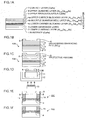
- Figs. 1A to 2B are schematics for illustrating a method of fabricating a semiconductor device according to an embodiment of the present invention.
- the semiconductor device is a semiconductor laser device having multiple quantum well (MQW) structure that outputs laser light within a wavelength band of 0.98 micrometer.
- the semiconductor laser device includes a lower cladding layer 2, a lower waveguide layer 3, an active layer 4, an upper waveguide layer 5, an upper cladding layer 6, and a contact layer 7 grown in this order on a substrate 1.
- the active layer 4 is formed by successively growing a lower carrier blocking layer 4c, a multiple quantum well layer 4b, and an upper carrier blocking layer 4a. Since the layers preferably have a superlattice structure, they are grown by metal organic chemical vapor deposition (MOCVD) or molecular beam epitaxy (MBE).
- MOCVD metal organic chemical vapor deposition
- MBE molecular beam epitaxy
- a method of fabricating the semiconductor laser device will be described according to the sequence of fabrication.
- a Al 0.08 Ga 0.92 As lower cladding layer 2 with a thickness of 2.4 micrometers is grown on a GaAs substrate 1.
- a GaAs lower waveguide layer 3 with a thickness of 0.48 micrometer is then grown on the lower cladding layer 2.
- An active layer 4 is then formed on the lower waveguide layer 3.
- the active layer 4 is formed by growing a Al 0.4 Ga 0.6 As lower carrier blocking layer 4a with a thickness of 0.035 micrometer, the multiple quantum well layer 4b with two stacked In 0.14 Ga 0.86 As layers each with a thickness of 0.01 micrometer on the lower carrier blocking layer 4a, and a Al 0.4 Ga 0.6 As upper carrier blocking layer 4c with a thickness of 0.035 micrometer on the multiple quantum well layer 4b.
- the GaAs upper waveguide layer 5 with a thickness of 0.45 micrometer is formed on the active layer 4, the Al 0.32 Ga 0.68 As upper cladding layer 6 with a thickness of 0.8 micrometer is formed on the upper waveguide layer 5, and a GaAs contact layer 7 with a film thickness of 0.3 micrometer is formed on the upper cladding layer 6.
- a disordering-enhancing film 8 made of SiO 2 is deposited on the entire upper portion of the contact layer 7 to a film thickness of 20 nanometers by using electron beam evaporation method. Thereafter, the disordering-enhancing film 8 is removed by using a photolithographic technique, except for portions corresponding to a window structure 14. As a result, as shown in Fig. 1B, the device substrate 10A with the disordering-enhancing film 8 deposited only on portions corresponding to the window structure 14 is obtained.
- the disordering-enhancing film 8 corresponds to the active layer 4 formed in a stripe shape, and is formed in a stripe with a width of 20 micrometers so as to cover the active layer 4.
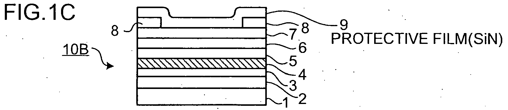
- a protective film 9 made of SiN x is deposited on the entire upper portion of the substrate including the disordering-enhancing film 8 to a thickness of 50 nanometers by using a catalytic CVD method.
- the device substrate 10B with the protective film 9 deposited thereon is obtained.
- the rapid thermal anneal (RTA) is performed on the device substrate 10B to cause disordering of the portion beneath the disordering-enhancing film 8, thereby to form a window structure 14 in that portion.
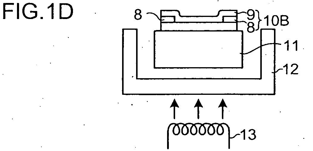
- the RTA is performed by placing the device substrate 10B on a mount 11 made of silicon carbide (SiC), arranging the mount 11 within a quartz tray 12, and heating a lamp heater 13 below the quartz tray 12 in a nitrogen (N 2 ) gas atmosphere to 930°C for 30 seconds.
- SiC silicon carbide
- N 2 nitrogen
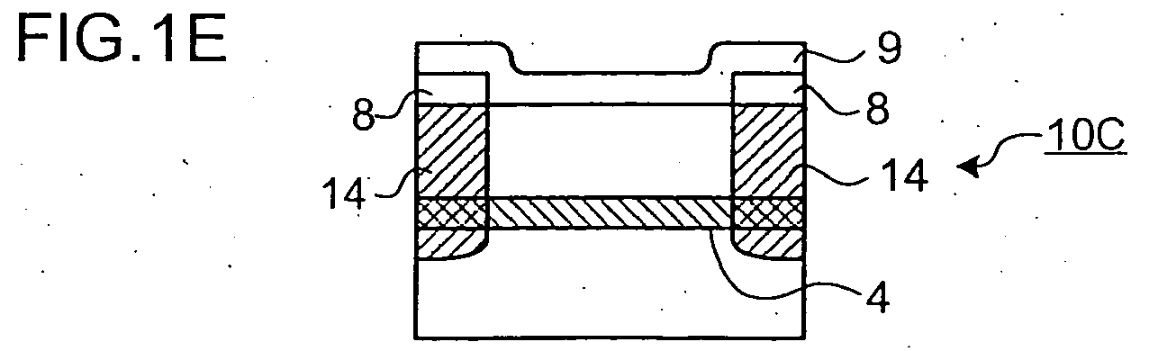
- gallium (Ga) atoms are absorbed from the respective layers under the disordering-enhancing film 8 into the disordering-enhancing film 8, leaving vacancies on the surface. The vacancies are diffused, particularly into the active layer 4 to disorder the active layer.
- a device substrate 10C with the window structure 14 is obtained.
- the protective film 9 and the disordering-enhancing film 8 are removed to obtain a device substrate 10D.
- an upper electrode 21 and a lower electrode 22 are then formed on the device substrate 10D to obtain a device substrate 10E with the electrode structure. The respective steps explained above are performed on the substrate 1.
- the device substrate 10E with the lower electrode 22 is cleaved along a broken line C shown in Fig. 2A, so that a laser bar containing a plurality of semiconductor laser devices is separated.
- a low reflection film 23 is coated for its emission side and a high reflection film 24 is coated for its reflection side.
- the laser bar is cut, in parallel with the paper surface of the drawing, into the respective semiconductor laser devices, to complete the fabrication of semiconductor laser devices 10.
- the protective film 9 made of SiN x is deposited using a catalytic CVD method.
- source gases for forming the protective film 9 are catalytically decomposed by a heated catalyzer and chemical reactions occur on a film to be formed. As a result, the protective film 9 is formed.
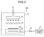
- Fig. 3 is a schematic of a catalytic CVD equipment 300.
- the catalytic CVD device 300 includes a chamber 31 in which the protective film 9 is deposited, a shower head 32 to introduce source gases for the protective film 9 into the chamber 31, a filament (tungsten wire) 33 serving as a heated catalyzer, a substrate holder 35 on which the substrate 1 is placed, a substrate heater 36 to heat the device substrate 10A, a vacuum pump 37 to evacuate the chamber 31, and a pressure adjustment valve 34 to adjust the pressure within the chamber 31.
- the tungsten wire 33 is placed between the shower head 32 and the substrate holder 35. After the pressure of the chamber 31 is reduced, source gases are introduced from the shower head 32 into the chamber 31, and contact the tungsten wire 33 to be decomposed thereat. The decomposed source gases flow on the device substrate 10A placed on the substrate holder 35.
- the device substrate 10A is placed on the substrate holder 35.
- the vacuum pump 37 is then operated and the pressure adjustment valve 34 is opened so that the pressure within the chamber 31 is reduced to a predetermined pressure.
- the substrate heater 36 is energized to maintain the temperature of the substrate at about 250°C.
- Ammonia (NH 3 ) gas is introduced via the shower head 32 into the chamber 31 at a flow rate of 200 sccm.
- the tungsten wire 33 is energized so as to maintain its temperature at 1680°C.
- Silane gas (SiH 4 ) is introduced via the shower head 32 into the chamber 31 at a flow rate.of 2 sccm and the pressure adjustment valve 34 is adjusted so as to maintain the pressure within the chamber 31 at 4.0 Pascals. 360 seconds thereafter, introduction of SiH 4 is stopped, energizing of the tungsten wire 33 is stopped, introduction of NH 3 is stopped, the pressure adjustment valve 34 is closed. Dry nitrogen gas (N 2 ) is introduced to return the pressure of the chamber 31 to atmospheric pressure.
- N 2 Dry nitrogen gas
- SiH 4 molecules and NH 3 molecules introduced into the chamber 31 contact the heated tungsten wire 33 to be decomposed into active SiH Y and NH Z , which reach onto the device substrate 10A. Since SiH Y and NH z are activated, chemical reactions proceed on the device substrate 10A at a relatively low temperature of 250°C, and thereby, SiN X is generated.
- the protective film 9 has a smaller amount of oxygen and hydrogen mixed therein and therefore has a higher compactness than films deposited by a PECVD method. In addition, since the protective film 9 is deposited at a lower temperature as compared to films deposited by thermal CVD method, its internal stress arising from thermal non-equilibrium is small. Thus, the protective film 9 has chemically and physically stable characteristics.
- Fig. 4 is a cross section of the device substrate 10B. As shown in Fig. 4, the protective film 9 is deposited on an upper portion of an area 14b where the window structure 14 is not formed.
- the above characteristics of the protective film 9 is helpful in preventing desorption of As atoms from a part of the active layer 4 corresponding to the area 14b. Therefore, during the process of RTA, a part of the active layer 4 corresponding to the area 14a is disordered while a part of the active layer 4 corresponding to the area 14b is not disordered.
- the process of disordering is selectively performed in a successful manner, with no damage on the multiple quantum well (MQW) structure of the active layer 4 and with no deterioration in performance of a laser light output.
- MQW multiple quantum well
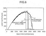
- Fig. 6 is a graph showing the difference in light-to-injection current characteristics between the semiconductor laser device with the window structure 14 and the semiconductor laser device without the window structure 14.
- an increase in injection current causes an increase in light output, which lead to an increase in the amount of heat generated.
- the increase in the amount of heat generated causes a thermal saturation of light output at the injection current of around 2000 to 2500 milliamperes, where COD occurs at the facet (see L2 in Fig. 6).
- COD occurs at the facet (see L2 in Fig. 6).
- the semiconductor laser device with the window structure 14 although the light output decreases due to thermal saturation, COD does not occur (see L1 in Fig. 6).
- the semiconductor laser device 10 can emit higher output power and enjoy longer lifetime. Particularly, the process of disordering to form the window structure in the fabricating method according to the embodiment does not affect the active layer 4, causing no deterioration in the light output performance of the semiconductor laser device 10.
- a device substrate 11B with a protective film 9a deposited.thereon so as to cover at least the area 14b may be used, as shown in Fig. 7. Namely, the protective film 9 may be deposited so as to cover at least the portion corresponding to the area 14b that is not to be subjected to a process of disordering.
- the present invention is not limited to such example but can be applied to performing the process of disordering by diffusing impurities such as Zn and Si by a thermal treatment.
- SiH 4 and NH 3 are used as materials (precursors) for depositing a SiN x film serving as the protective film 9 in this embodiment, the present invention is not limited to such materials.
- Precursors containing Si and N can be used or precursors prepared by combining Si with NH 3 can be used.
- the present invention is not limited to forming the window structure.
- the present invention can be generally applied to disordering of local areas.
- the heating temperature of the tungsten wire 33 may be higher than a temperature above which the tungsten wire 33 is not silicided and lower than a temperature below which a vapor pressure of the tungsten wire 33 does not affect deposition of the protective film 9. Therefore, the heating temperature of the tungsten wire 33 can be set to between 1600°C and 1900°C, for example.
- a flow rate of NH 3 gas to SiH 4 , a pressure within the chamber 31, and the like can be set optimally to realize high compactness of the protective film 9.
- the semiconductor laser device 10 is not limited to one of a particular laser structure or of a particular composition, but may generally be a semiconductor laser device of any structure. While a composition of an active area used for the semiconductor laser device 10 can be selected from GaAs, AlGaAs, InGaAs, InAlGaAs, InGaAsP, and the like depending on oscillation wavelengths, other compositions can be used.
- a method of fabricating a semiconductor device such as a semiconductor laser device, in which only a portion to be partially disordered, such as a portion to be a window structure, is disordered with no adverse effect on the other portions not to be disordered, and thereby to provide a method of fabricating a semiconductor device of high output power, long lifetime, and high reliability.
- the present invention is suitable for a semiconductor device that includes a portion to be partially disordered such as a window structure in a semiconductor laser device, and is suitable for fabricating such semiconductor devices.
Landscapes
- Physics & Mathematics (AREA)
- Condensed Matter Physics & Semiconductors (AREA)
- General Physics & Mathematics (AREA)
- Electromagnetism (AREA)
- Optics & Photonics (AREA)
- Semiconductor Lasers (AREA)
- Formation Of Insulating Films (AREA)
Abstract


Description
- The present invention relates to a method of fabricating a semiconductor device that includes a portion to be partially disordered, such as a window structure in a semiconductor laser device, by using a thin film deposition method such as the catalytic chemical vapor deposition (CVD) method or the hot wire cell method, which are capable of depositing a thin film of high compactness at low temperatures.
- Conventionally, light-emitting facets of semiconductor laser devices are susceptible to a catastrophic optical damage (COD). The COD is a phenomenon in which a feedback cycle of: increase in temperature of a facet → shrinkage of band gap → light absorption → recombination current flow → increase in temperature of the facet, is created on an emitting-side facet of an active layer, which becomes a positive feedback to cause melting and instantaneous deterioration of the facet.
- A window structure is usually formed at the emitting-side facet of the active layer in order to prevent such COD. The window structure broadens an energy band gap in the emitting-side facet, whereby the facet has less absorption of laser light. As a result, the COD is suppressed and a semiconductor laser device with long lifetime is realized.
- The window structure has been conventionally formed by an independent semiconductor process. For example, a portion where the window structure is to be formed is removed by etching or the like, and thereafter, materials with property corresponding to the window structure are embedded into the portion. The forming of the window structure is also achieved by disordering a portion to be the window structure. When the active layer has a superlattice structure, the process of disordering is performed by introducing impurities by an ion implantation or a thermal treatment into the superlattice structure of a portion where the window structure is to be formed, followed by a thermal treatment with a dielectric film to generate lattice vacancies so that constitutional elements of the respective layers that are spatially separated by hetero interfaces are mixed. The disordered portion exhibits properties different from those before implementing the process of disordering. For example, the portion has different band-gap energy and different refractive index (see Japanese Patent Application Laid-Open No. 2000-208870).
- However, when the window structure is formed by the process of disordering, a thermal treatment must be performed for diffusion of impurities or vacancies. Since the thermal treatment is performed for the entire semiconductor laser device, the thermal treatment adversely affects portions that do not need to be disordered, causing deterioration of performance of the semiconductor laser device.
- When the active layer is made of AlGaAs based materials and a part of the active layer is disordered by depositing a silicon dioxide (SiO2) film, which serves an enhance film for disordering, on an upper surface of the window structure to be disordered, arsenic (As) atoms are desorbed from a device surface corresponding to the active layer that is not to be disordered and the surface is roughened. When an electrode is formed on a contact layer, favorable contact between the electrode and the contact layer is not assured and a laser oscillation performance is deteriorated.
- Particularly, desorbed As atoms from GaAs contact layer of the device surface leaves pits, which are a cause of dislocation defects that grow through non-radiative recombination to reach the active layer, which also deteriorates the laser oscillation performance.
- Conventionally, deposition of silicon nitride (SiNx) by plasma-enhanced chemical vapor deposition (PECVD) method on the entire upper surface of a semiconductor laser device, so as to function as a heat-resistant protective film, is considered as a method of preventing desorption of As. However, the PECVD method is likely to cause plasma damage on the surface of the semiconductor device, which generates a dislocation defect. Furthermore, the deposited film is coarse and does not sufficiently function as the heat-resistant protective film.
- In view of the above problems, an object of the present invention is to provide a method of fabricating a semiconductor device such as a semiconductor laser device, in which only a portion to be partially disordered, such as a portion to be a window structure, is disordered with no adverse effect on the other portions not to be disordered, and thereby to provide a method of fabricating a semiconductor device of high output power, long lifetime, and high reliability.
- To solve the above problems and to achieve the object, a method of fabricating a semiconductor device that includes a disordered portion, according to one aspect of the present invention, includes the step of forming a protective film on a surface of the semiconductor device corresponding to at least a portion that is not to be disordered, by arranging a heat source on a path through which a precursor of the protective film to be formed passes, to cause a decomposition reaction of the precursor in the presence of the heat source, and exposing the surface of the semiconductor device to the atmosphere after the decomposition reaction; and the step of disordering the portion to be disordered using a thermal treatment.
- Furthermore, according to the present invention, the semiconductor device is a semiconductor laser device that includes a window structure as the disordered portion, and an active layer of quantum well structure as the portion not to be disordered.
- Moreover, the present invention includes the step of pretreatment in which a disordering-enhancing film is formed adjacent to a portion to be disordered, and the step of forming a protective film comprises the step of forming a protective film adjacent to at least a portion that is not to be disordered.
- Furthermore, according to the present invention, the disordering-enhancing film is made of silicon dioxide (SiO2).
- Moreover, according to the present invention, the step of forming a protective film includes forming the protective film using a catalytic chemical-vapor-deposition method.
- Furthermore, according to the present invention, the precursor is a compound containing nitrogen and silicon.
- Moreover, according to the present invention, the precursor is a mixture of a nitrogen compound and a silicon compound.
-
- Figs. 1A to 1F are schematics for illustrating a method of fabricating a semiconductor device according to an embodiment of the present invention;
- Figs. 2A and 2B are schematics for illustrating the method of fabricating a semiconductor device according to the embodiment;
- Fig. 3 is a schematic of a catalytic CVD equipment, used in the method according to the embodiment;
- Fig. 4 is a schematic for illustrating phenomena to occur in a portion to be disordered and a potion not to be disordered, in the method according to the embodiment;
- Fig. 5 is a schematic for illustrating pits and cracks generated by the pits in a semiconductor device;
- Fig. 6 is a graph of injection current versus light output of a semiconductor laser device with and without a window structure according to the embodiment; and
- Fig. 7 is a schematic for illustrating an example of depositing a protective film that covers at least the potion not to be disordered, in the method according to the embodiment.
- Exemplary embodiments of the present invention will be explained in detail below with reference to the accompanying drawings. The invention is not limited to the embodiments.
- Figs. 1A to 2B are schematics for illustrating a method of fabricating a semiconductor device according to an embodiment of the present invention. The semiconductor device is a semiconductor laser device having multiple quantum well (MQW) structure that outputs laser light within a wavelength band of 0.98 micrometer. The semiconductor laser device includes a
lower cladding layer 2, alower waveguide layer 3, anactive layer 4, anupper waveguide layer 5, anupper cladding layer 6, and acontact layer 7 grown in this order on asubstrate 1. Theactive layer 4 is formed by successively growing a lower carrier blocking layer 4c, a multiple quantum well layer 4b, and an upper carrier blocking layer 4a. Since the layers preferably have a superlattice structure, they are grown by metal organic chemical vapor deposition (MOCVD) or molecular beam epitaxy (MBE). - First, a method of fabricating the semiconductor laser device will be described according to the sequence of fabrication. As shown in Fig. 1A, a Al0.08Ga0.92As
lower cladding layer 2 with a thickness of 2.4 micrometers is grown on aGaAs substrate 1. A GaAslower waveguide layer 3 with a thickness of 0.48 micrometer is then grown on thelower cladding layer 2. Anactive layer 4 is then formed on thelower waveguide layer 3. - The
active layer 4 is formed by growing a Al0.4Ga0.6As lower carrier blocking layer 4a with a thickness of 0.035 micrometer, the multiple quantum well layer 4b with two stacked In0.14Ga0.86As layers each with a thickness of 0.01 micrometer on the lower carrier blocking layer 4a, and a Al0.4Ga0.6As upper carrier blocking layer 4c with a thickness of 0.035 micrometer on the multiple quantum well layer 4b. - The GaAs
upper waveguide layer 5 with a thickness of 0.45 micrometer is formed on theactive layer 4, the Al0.32Ga0.68Asupper cladding layer 6 with a thickness of 0.8 micrometer is formed on theupper waveguide layer 5, and aGaAs contact layer 7 with a film thickness of 0.3 micrometer is formed on theupper cladding layer 6. - After the
contact layer 7 with a superlattice structure is formed, a disordering-enhancingfilm 8 made of SiO2 is deposited on the entire upper portion of thecontact layer 7 to a film thickness of 20 nanometers by using electron beam evaporation method. Thereafter, the disordering-enhancingfilm 8 is removed by using a photolithographic technique, except for portions corresponding to awindow structure 14. As a result, as shown in Fig. 1B, thedevice substrate 10A with the disordering-enhancingfilm 8 deposited only on portions corresponding to thewindow structure 14 is obtained. The disordering-enhancingfilm 8 corresponds to theactive layer 4 formed in a stripe shape, and is formed in a stripe with a width of 20 micrometers so as to cover theactive layer 4. - As shown in Fig. 1C, a
protective film 9 made of SiNx is deposited on the entire upper portion of the substrate including the disordering-enhancingfilm 8 to a thickness of 50 nanometers by using a catalytic CVD method. As a result, thedevice substrate 10B with theprotective film 9 deposited thereon is obtained. Thereafter, the rapid thermal anneal (RTA) is performed on thedevice substrate 10B to cause disordering of the portion beneath the disordering-enhancingfilm 8, thereby to form awindow structure 14 in that portion. - As shown in Fig. 1D, the RTA is performed by placing the
device substrate 10B on amount 11 made of silicon carbide (SiC), arranging themount 11 within aquartz tray 12, and heating alamp heater 13 below thequartz tray 12 in a nitrogen (N2) gas atmosphere to 930°C for 30 seconds. - During the process of RTA, gallium (Ga) atoms are absorbed from the respective layers under the disordering-enhancing
film 8 into the disordering-enhancingfilm 8, leaving vacancies on the surface. The vacancies are diffused, particularly into theactive layer 4 to disorder the active layer. By the process, as shown in Fig. 1E, adevice substrate 10C with thewindow structure 14 is obtained. - After the
window structure 14 is formed, as shown in Fig. 1F, theprotective film 9 and the disordering-enhancingfilm 8 are removed to obtain adevice substrate 10D. Thereafter, as shown in Fig. 2A, anupper electrode 21 and alower electrode 22 are then formed on thedevice substrate 10D to obtain adevice substrate 10E with the electrode structure. The respective steps explained above are performed on thesubstrate 1. - The
device substrate 10E with thelower electrode 22 is cleaved along a broken line C shown in Fig. 2A, so that a laser bar containing a plurality of semiconductor laser devices is separated. As shown in Fig. 2B, on the cleavage surfaces of the separated laser bar, alow reflection film 23 is coated for its emission side and ahigh reflection film 24 is coated for its reflection side. The laser bar is cut, in parallel with the paper surface of the drawing, into the respective semiconductor laser devices, to complete the fabrication ofsemiconductor laser devices 10. - A method of depositing the
protective film 9 is explained next. Theprotective film 9 made of SiNx is deposited using a catalytic CVD method. According to the catalytic CVD method, source gases for forming theprotective film 9 are catalytically decomposed by a heated catalyzer and chemical reactions occur on a film to be formed. As a result, theprotective film 9 is formed. - Fig. 3 is a schematic of a
catalytic CVD equipment 300. As shown in Fig. 3, thecatalytic CVD device 300 includes achamber 31 in which theprotective film 9 is deposited, ashower head 32 to introduce source gases for theprotective film 9 into thechamber 31, a filament (tungsten wire) 33 serving as a heated catalyzer, asubstrate holder 35 on which thesubstrate 1 is placed, asubstrate heater 36 to heat thedevice substrate 10A, avacuum pump 37 to evacuate thechamber 31, and apressure adjustment valve 34 to adjust the pressure within thechamber 31. The tungsten wire 33 is placed between theshower head 32 and thesubstrate holder 35. After the pressure of thechamber 31 is reduced, source gases are introduced from theshower head 32 into thechamber 31, and contact the tungsten wire 33 to be decomposed thereat. The decomposed source gases flow on thedevice substrate 10A placed on thesubstrate holder 35. - Next, a process of depositing the
protective film 9 is explained below. Thedevice substrate 10A is placed on thesubstrate holder 35. Thevacuum pump 37 is then operated and thepressure adjustment valve 34 is opened so that the pressure within thechamber 31 is reduced to a predetermined pressure. When the pressure within thechamber 31 is reduced to the predetermined pressure, thesubstrate heater 36 is energized to maintain the temperature of the substrate at about 250°C. - Ammonia (NH3) gas is introduced via the
shower head 32 into thechamber 31 at a flow rate of 200 sccm. The tungsten wire 33 is energized so as to maintain its temperature at 1680°C. Silane gas (SiH4) is introduced via theshower head 32 into thechamber 31 at a flow rate.of 2 sccm and thepressure adjustment valve 34 is adjusted so as to maintain the pressure within thechamber 31 at 4.0 Pascals. 360 seconds thereafter, introduction of SiH4 is stopped, energizing of the tungsten wire 33 is stopped, introduction of NH3 is stopped, thepressure adjustment valve 34 is closed. Dry nitrogen gas (N2) is introduced to return the pressure of thechamber 31 to atmospheric pressure. Thus, thedevice substrate 10B with the 50 nanometer-thick SiNxprotective film 9 formed thereon is obtained. - During the above process, SiH4 molecules and NH3 molecules introduced into the
chamber 31 contact the heated tungsten wire 33 to be decomposed into active SiHY and NHZ, which reach onto thedevice substrate 10A. Since SiHY and NHz are activated, chemical reactions proceed on thedevice substrate 10A at a relatively low temperature of 250°C, and thereby, SiNX is generated. - The
protective film 9 has a smaller amount of oxygen and hydrogen mixed therein and therefore has a higher compactness than films deposited by a PECVD method. In addition, since theprotective film 9 is deposited at a lower temperature as compared to films deposited by thermal CVD method, its internal stress arising from thermal non-equilibrium is small. Thus, theprotective film 9 has chemically and physically stable characteristics. - Effects of the
protective film 9 are explained next. Fig. 4 is a cross section of thedevice substrate 10B. As shown in Fig. 4, theprotective film 9 is deposited on an upper portion of anarea 14b where thewindow structure 14 is not formed. When RTA is performed for the purpose of disordering, the above characteristics of theprotective film 9 is helpful in preventing desorption of As atoms from a part of theactive layer 4 corresponding to thearea 14b. Therefore, during the process of RTA, a part of theactive layer 4 corresponding to thearea 14a is disordered while a part of theactive layer 4 corresponding to thearea 14b is not disordered. With theprotective film 9, the process of disordering is selectively performed in a successful manner, with no damage on the multiple quantum well (MQW) structure of theactive layer 4 and with no deterioration in performance of a laser light output. - Moreover, as shown in Fig. 5, since desorption of As atoms in the
area 14b is prevented, the surface of theupper contact layer 7 is smooth and free frompits 41 due to the desorption of As atoms. Consequently, the device is free from cracks generated due to thepits 41 and favorable contact between thecontact layer 7 and theupper electrode 21 is assured. - Fig. 6 is a graph showing the difference in light-to-injection current characteristics between the semiconductor laser device with the
window structure 14 and the semiconductor laser device without thewindow structure 14. As shown in Fig. 6, in the semiconductor laser device without thewindow structure 14, an increase in injection current causes an increase in light output, which lead to an increase in the amount of heat generated. The increase in the amount of heat generated causes a thermal saturation of light output at the injection current of around 2000 to 2500 milliamperes, where COD occurs at the facet (see L2 in Fig. 6). On the other hand, in the semiconductor laser device with thewindow structure 14, although the light output decreases due to thermal saturation, COD does not occur (see L1 in Fig. 6). Since the laser light output facet is strengthened by thewindow structure 14, thesemiconductor laser device 10 can emit higher output power and enjoy longer lifetime. Particularly, the process of disordering to form the window structure in the fabricating method according to the embodiment does not affect theactive layer 4, causing no deterioration in the light output performance of thesemiconductor laser device 10. - While the
protective film 9 is deposited so as to cover the entire surface of the device substrate in this embodiment, adevice substrate 11B with aprotective film 9a deposited.thereon so as to cover at least thearea 14b may be used, as shown in Fig. 7. Namely, theprotective film 9 may be deposited so as to cover at least the portion corresponding to thearea 14b that is not to be subjected to a process of disordering. - While in this embodiment is described an example in which the process of disordering is performed with the disordering-enhancing
film 8 deposited, the present invention is not limited to such example but can be applied to performing the process of disordering by diffusing impurities such as Zn and Si by a thermal treatment. - While SiH4 and NH3 are used as materials (precursors) for depositing a SiNx film serving as the
protective film 9 in this embodiment, the present invention is not limited to such materials. Precursors containing Si and N can be used or precursors prepared by combining Si with NH3 can be used. - While a process of disordering to form a window structure of the
semiconductor laser device 10 is described in this embodiment, the present invention is not limited to forming the window structure. The present invention can be generally applied to disordering of local areas. - While a heating temperature of the tungsten wire.33 is set to 1680°C in this embodiment, the heating temperature of the tungsten wire 33 may be higher than a temperature above which the tungsten wire 33 is not silicided and lower than a temperature below which a vapor pressure of the tungsten wire 33 does not affect deposition of the
protective film 9. Therefore, the heating temperature of the tungsten wire 33 can be set to between 1600°C and 1900°C, for example. - A flow rate of NH3 gas to SiH4, a pressure within the
chamber 31, and the like can be set optimally to realize high compactness of theprotective film 9. - The
semiconductor laser device 10 is not limited to one of a particular laser structure or of a particular composition, but may generally be a semiconductor laser device of any structure. While a composition of an active area used for thesemiconductor laser device 10 can be selected from GaAs, AlGaAs, InGaAs, InAlGaAs, InGaAsP, and the like depending on oscillation wavelengths, other compositions can be used. - As described above, according to the present invention, a method of fabricating a semiconductor device such as a semiconductor laser device, in which only a portion to be partially disordered, such as a portion to be a window structure, is disordered with no adverse effect on the other portions not to be disordered, and thereby to provide a method of fabricating a semiconductor device of high output power, long lifetime, and high reliability.
- As described above, the present invention is suitable for a semiconductor device that includes a portion to be partially disordered such as a window structure in a semiconductor laser device, and is suitable for fabricating such semiconductor devices.
Claims (11)
- A method of fabricating a semiconductor device that includes a disordered portion, the method comprising:forming a protective film on a surface of the semiconductor device corresponding to at least a portion that is not to be disordered, by arranging a heat source on a path through which a precursor of the protective film to be formed passes, to cause a decomposition reaction of the precursor in the presence of the heat source, and by exposing the surface of the semiconductor device to the atmosphere after the decomposition reaction; anddisordering the portion to be disordered using a thermal treatment.
- The method according to claim 1, wherein the semiconductor device is a semiconductor laser device that includes a window structure as the disordered portion and an active layer of quantum well structure as the portion not to be disordered.
- The method according to claim 1, wherein the forming the protective,film includes forming the protective film using a catalytic chemical-vapor-deposition method.
- The method according to claim 1, wherein the precursor is a compound containing nitrogen and silicon.
- The method according to claim 1, wherein the precursor is a mixture of a nitrogen compound and a silicon compound.
- A method of fabricating a semiconductor device that includes a window structure as a disordered portion, the method comprising:forming a disordering-enhancing film on a surface of the semiconductor device covering a portion to be disordered;forming a protective film on the surface of the semiconductor device covering at least a portion not to be disordered, by arranging a heat source on a path through which a precursor of the protective film to be formed passes, to cause a decomposition reaction of the precursor in the presence of the heat source, and by exposing the surface of the semiconductor device to the atmosphere after the decomposition reaction; anddisordering the portion to be disordered in the semiconductor device using a thermal treatment.
- The method according to claim 6, wherein the semiconductor device is a semiconductor laser device that includes a window structure as the disorderd portion and an active layer of quantum well structure as the portion not to be disordered.
- The method according to claim 6, wherein the disordering-enhancing film is made of silicon dioxide.
- The method according to claim 6, wherein the forming the protective film includes forming the protective film using a catalytic chemical-vapor-deposition method.
- The method according to claim 6, wherein the precursor is a compound containing nitrogen and silicon.
- The method according to claim 6, wherein the precursor is a mixture of a nitrogen compound and a silicon compound.
Applications Claiming Priority (2)
| Application Number | Priority Date | Filing Date | Title |
|---|---|---|---|
| JP2003114841A JP4128898B2 (en) | 2003-04-18 | 2003-04-18 | Manufacturing method of semiconductor device |
| PCT/JP2004/005542 WO2004093274A1 (en) | 2003-04-18 | 2004-04-19 | Method of manufacturing semiconductor device |
Publications (3)
| Publication Number | Publication Date |
|---|---|
| EP1617533A1 true EP1617533A1 (en) | 2006-01-18 |
| EP1617533A4 EP1617533A4 (en) | 2006-06-21 |
| EP1617533B1 EP1617533B1 (en) | 2010-12-22 |
Family
ID=33296162
Family Applications (1)
| Application Number | Title | Priority Date | Filing Date |
|---|---|---|---|
| EP04728254A Expired - Lifetime EP1617533B1 (en) | 2003-04-18 | 2004-04-19 | Method of manufacturing a semiconductor device |
Country Status (6)
| Country | Link |
|---|---|
| US (1) | US20060039430A1 (en) |
| EP (1) | EP1617533B1 (en) |
| JP (1) | JP4128898B2 (en) |
| CN (1) | CN100407524C (en) |
| DE (1) | DE602004030677D1 (en) |
| WO (1) | WO2004093274A1 (en) |
Families Citing this family (5)
| Publication number | Priority date | Publication date | Assignee | Title |
|---|---|---|---|---|
| EP1699121B1 (en) * | 2003-12-15 | 2014-04-30 | The Furukawa Electric Co., Ltd. | Semiconductor device manufacturing method |
| US7564563B2 (en) | 2006-06-02 | 2009-07-21 | Advanced Telecommunications Research Institute International | Laser gyro and electronic device using the same |
| CN101796699B (en) * | 2007-09-04 | 2012-12-26 | 古河电气工业株式会社 | Semiconductor laser element, and semiconductor laser element manufacturing method |
| JP7379334B2 (en) | 2018-07-27 | 2023-11-14 | ヌヴォトンテクノロジージャパン株式会社 | Semiconductor laser device, inspection method and inspection equipment |
| JP7672258B2 (en) | 2021-03-26 | 2025-05-07 | 古河電気工業株式会社 | Semiconductor laser device and method for manufacturing the same |
Family Cites Families (17)
| Publication number | Priority date | Publication date | Assignee | Title |
|---|---|---|---|---|
| FR2371777A1 (en) * | 1976-11-18 | 1978-06-16 | Loic Henry | METHOD OF MANUFACTURING A SILICON NITRIDE DIFFUSION BARRIER ON A SEMICONDUCTOR SUBSTRATE, IN PARTICULAR OF THE III-V TYPE |
| US4796082A (en) * | 1987-03-16 | 1989-01-03 | International Business Machines Corporation | Thermally stable ohmic contact for gallium-arsenide |
| US4990466A (en) * | 1988-11-01 | 1991-02-05 | Siemens Corporate Research, Inc. | Method for fabricating index-guided semiconductor laser |
| JPH05110185A (en) * | 1991-10-14 | 1993-04-30 | Fuji Xerox Co Ltd | Semiconductor laser device |
| JPH07154026A (en) * | 1993-11-30 | 1995-06-16 | Fuji Xerox Co Ltd | Semiconductor laser and fabrication thereof |
| US5708674A (en) * | 1995-01-03 | 1998-01-13 | Xerox Corporation | Semiconductor laser or array formed by layer intermixing |
| JP3141805B2 (en) * | 1997-01-20 | 2001-03-07 | 日本電気株式会社 | Method for manufacturing semiconductor device |
| JP2001185809A (en) * | 1999-12-24 | 2001-07-06 | Mitsubishi Chemicals Corp | Semiconductor optical device and manufacturing method thereof |
| US6703254B2 (en) * | 2000-08-22 | 2004-03-09 | Mitsui Chemicals, Inc. | Method for manufacturing semiconductor laser device |
| JP2002075992A (en) * | 2000-09-01 | 2002-03-15 | Fujitsu Ltd | Method for forming silicon nitride film, method for manufacturing semiconductor device, and semiconductor device |
| US6878562B2 (en) * | 2000-10-20 | 2005-04-12 | Phosistor Technologies, Incorporated | Method for shifting the bandgap energy of a quantum well layer |
| GB2372148A (en) * | 2001-01-23 | 2002-08-14 | Univ Glasgow | A Method of Manufacturing an Optical Device |
| US6834068B2 (en) * | 2001-06-29 | 2004-12-21 | Matsushita Electric Industrial Co., Ltd. | Semiconductor laser device and method for fabricating the same |
| JP2003086894A (en) * | 2001-06-29 | 2003-03-20 | Matsushita Electric Ind Co Ltd | Semiconductor laser device and method of manufacturing the same |
| US20030064537A1 (en) * | 2001-09-28 | 2003-04-03 | The Furukawa Electric Co., Ltd. | Semiconductor laser device and method for effectively reducing facet reflectivity |
| US6674778B1 (en) * | 2002-01-09 | 2004-01-06 | Sandia Corporation | Electrically pumped edge-emitting photonic bandgap semiconductor laser |
| JP3868324B2 (en) * | 2002-04-15 | 2007-01-17 | 三菱電機株式会社 | Silicon nitride film forming method, film forming apparatus, and semiconductor device manufacturing method |
-
2003
- 2003-04-18 JP JP2003114841A patent/JP4128898B2/en not_active Expired - Lifetime
-
2004
- 2004-04-19 DE DE602004030677T patent/DE602004030677D1/en not_active Expired - Lifetime
- 2004-04-19 EP EP04728254A patent/EP1617533B1/en not_active Expired - Lifetime
- 2004-04-19 CN CN2004800065693A patent/CN100407524C/en not_active Expired - Lifetime
- 2004-04-19 WO PCT/JP2004/005542 patent/WO2004093274A1/en not_active Ceased
-
2005
- 2005-10-14 US US11/249,386 patent/US20060039430A1/en not_active Abandoned
Also Published As
| Publication number | Publication date |
|---|---|
| US20060039430A1 (en) | 2006-02-23 |
| EP1617533B1 (en) | 2010-12-22 |
| JP2004319914A (en) | 2004-11-11 |
| EP1617533A4 (en) | 2006-06-21 |
| WO2004093274A1 (en) | 2004-10-28 |
| JP4128898B2 (en) | 2008-07-30 |
| CN100407524C (en) | 2008-07-30 |
| CN1759509A (en) | 2006-04-12 |
| DE602004030677D1 (en) | 2011-02-03 |
Similar Documents
| Publication | Publication Date | Title |
|---|---|---|
| US7777216B2 (en) | Method of fabricating semiconductor device | |
| JP3833674B2 (en) | Nitride semiconductor laser device | |
| JP2004538652A (en) | Contaminant laser mirrors and methods of obtaining their passivation | |
| EP2187488B1 (en) | Semiconductor laser element, and semiconductor laser element manufacturing method | |
| JP4100592B2 (en) | Group III or group III-V nitride layer growth method and electronic device | |
| JPH1056236A (en) | Group III nitride semiconductor laser device | |
| US9627849B2 (en) | Semiconductor light device and manufacturing method for the same | |
| EP1006629A2 (en) | Compound semiconductor light emitting device | |
| JP5302250B2 (en) | Method for MOCVD growth of compounds containing GaAsN alloys using an ammonia precursor with a catalyst | |
| JPWO2002017450A1 (en) | Semiconductor laser element manufacturing method | |
| WO2002017450A1 (en) | Method for manufacturing semiconductor laser device | |
| EP1617533B1 (en) | Method of manufacturing a semiconductor device | |
| JP2000208814A (en) | Semiconductor light emitting device | |
| US6235548B1 (en) | Method of fabricating nitride semiconductor laser | |
| US7720124B2 (en) | Semiconductor device and fabrication method thereof | |
| JP2005203411A (en) | Nitride semiconductor light emitting device | |
| JP3717255B2 (en) | Group 3 nitride semiconductor laser device | |
| EP1109231A2 (en) | Semiconductor light emitter and method for fabricating the same | |
| US7026183B2 (en) | Long-wavelength semiconductor light emitting device and its manufacturing method | |
| US20040115854A1 (en) | Method of MOCVD growth of compounds including GaAsN alloys using an ammonia precursor and radiation | |
| CN121688554A (en) | Micro-disc structure semiconductor laser and preparation method thereof | |
| JP2008294223A (en) | Method for growing III-V compound semiconductor film | |
| JPH08130186A (en) | Method for manufacturing p-type II-VI compound semiconductor | |
| JP2010225727A (en) | Manufacturing method of nitride semiconductor laser |
Legal Events
| Date | Code | Title | Description |
|---|---|---|---|
| PUAI | Public reference made under article 153(3) epc to a published international application that has entered the european phase |
Free format text: ORIGINAL CODE: 0009012 |
|
| 17P | Request for examination filed |
Effective date: 20051013 |
|
| AK | Designated contracting states |
Kind code of ref document: A1 Designated state(s): AT BE BG CH CY CZ DE DK EE ES FI FR GB GR HU IE IT LI LU MC NL PL PT RO SE SI SK TR |
|
| AX | Request for extension of the european patent |
Extension state: AL HR LT LV MK |
|
| RIN1 | Information on inventor provided before grant (corrected) |
Inventor name: IZUMI, AKIRA Inventor name: YAMADA, YUMI, 2-3-15-202, HAKAMATSUKA |
|
| RAP1 | Party data changed (applicant data changed or rights of an application transferred) |
Owner name: FURUKAWA ELECTRIC CO., LTD. Owner name: MITSUI CHEMICALS, INC. |
|
| RIN1 | Information on inventor provided before grant (corrected) |
Inventor name: IZUMI, AKIRA Inventor name: YAMADA, YUMI, |
|
| A4 | Supplementary search report drawn up and despatched |
Effective date: 20060519 |
|
| DAX | Request for extension of the european patent (deleted) | ||
| RBV | Designated contracting states (corrected) |
Designated state(s): DE |
|
| 17Q | First examination report despatched |
Effective date: 20060905 |
|
| RIN1 | Information on inventor provided before grant (corrected) |
Inventor name: YAMADA, YUMI, Inventor name: IZUMI, AKIRA |
|
| RAP1 | Party data changed (applicant data changed or rights of an application transferred) |
Owner name: THE FURUKAWA ELECTRIC CO., LTD. |
|
| RTI1 | Title (correction) |
Free format text: METHOD OF MANUFACTURING A SEMICONDUCTOR DEVICE |
|
| GRAP | Despatch of communication of intention to grant a patent |
Free format text: ORIGINAL CODE: EPIDOSNIGR1 |
|
| GRAS | Grant fee paid |
Free format text: ORIGINAL CODE: EPIDOSNIGR3 |
|
| GRAA | (expected) grant |
Free format text: ORIGINAL CODE: 0009210 |
|
| AK | Designated contracting states |
Kind code of ref document: B1 Designated state(s): DE |
|
| REF | Corresponds to: |
Ref document number: 602004030677 Country of ref document: DE Date of ref document: 20110203 Kind code of ref document: P |
|
| REG | Reference to a national code |
Ref country code: DE Ref legal event code: R096 Ref document number: 602004030677 Country of ref document: DE Effective date: 20110203 |
|
| PLBE | No opposition filed within time limit |
Free format text: ORIGINAL CODE: 0009261 |
|
| STAA | Information on the status of an ep patent application or granted ep patent |
Free format text: STATUS: NO OPPOSITION FILED WITHIN TIME LIMIT |
|
| 26N | No opposition filed |
Effective date: 20110923 |
|
| REG | Reference to a national code |
Ref country code: DE Ref legal event code: R097 Ref document number: 602004030677 Country of ref document: DE Effective date: 20110923 |
|
| P01 | Opt-out of the competence of the unified patent court (upc) registered |
Effective date: 20230512 |
|
| PGFP | Annual fee paid to national office [announced via postgrant information from national office to epo] |
Ref country code: DE Payment date: 20230228 Year of fee payment: 20 |
|
| REG | Reference to a national code |
Ref country code: DE Ref legal event code: R071 Ref document number: 602004030677 Country of ref document: DE |