EP1617466A1 - Method for producing single crystal ingot from which semiconductor wafer is sliced - Google Patents
Method for producing single crystal ingot from which semiconductor wafer is sliced Download PDFInfo
- Publication number
- EP1617466A1 EP1617466A1 EP04747582A EP04747582A EP1617466A1 EP 1617466 A1 EP1617466 A1 EP 1617466A1 EP 04747582 A EP04747582 A EP 04747582A EP 04747582 A EP04747582 A EP 04747582A EP 1617466 A1 EP1617466 A1 EP 1617466A1
- Authority
- EP
- European Patent Office
- Prior art keywords
- crystal semiconductor
- diameter
- crystal
- small
- blocks
- Prior art date
- Legal status (The legal status is an assumption and is not a legal conclusion. Google has not performed a legal analysis and makes no representation as to the accuracy of the status listed.)
- Withdrawn
Links
Images

Classifications
-
- B—PERFORMING OPERATIONS; TRANSPORTING
- B28—WORKING CEMENT, CLAY, OR STONE
- B28D—WORKING STONE OR STONE-LIKE MATERIALS
- B28D1/00—Working stone or stone-like materials, e.g. brick, concrete or glass, not provided for elsewhere; Machines, devices, tools therefor
- B28D1/02—Working stone or stone-like materials, e.g. brick, concrete or glass, not provided for elsewhere; Machines, devices, tools therefor by sawing
- B28D1/04—Working stone or stone-like materials, e.g. brick, concrete or glass, not provided for elsewhere; Machines, devices, tools therefor by sawing with circular or cylindrical saw-blades or saw-discs
- B28D1/041—Working stone or stone-like materials, e.g. brick, concrete or glass, not provided for elsewhere; Machines, devices, tools therefor by sawing with circular or cylindrical saw-blades or saw-discs with cylinder saws, e.g. trepanning; saw cylinders, e.g. having their cutting rim equipped with abrasive particles
-
- H—ELECTRICITY
- H10—SEMICONDUCTOR DEVICES; ELECTRIC SOLID-STATE DEVICES NOT OTHERWISE PROVIDED FOR
- H10P—GENERIC PROCESSES OR APPARATUS FOR THE MANUFACTURE OR TREATMENT OF DEVICES COVERED BY CLASS H10
- H10P52/00—Grinding, lapping or polishing of wafers, substrates or parts of devices
-
- B—PERFORMING OPERATIONS; TRANSPORTING
- B28—WORKING CEMENT, CLAY, OR STONE
- B28D—WORKING STONE OR STONE-LIKE MATERIALS
- B28D5/00—Fine working of gems, jewels, crystals, e.g. of semiconductor material; apparatus or devices therefor
- B28D5/04—Fine working of gems, jewels, crystals, e.g. of semiconductor material; apparatus or devices therefor by tools other than rotary type, e.g. reciprocating tools
-
- C—CHEMISTRY; METALLURGY
- C30—CRYSTAL GROWTH
- C30B—SINGLE-CRYSTAL GROWTH; UNIDIRECTIONAL SOLIDIFICATION OF EUTECTIC MATERIAL OR UNIDIRECTIONAL DEMIXING OF EUTECTOID MATERIAL; REFINING BY ZONE-MELTING OF MATERIAL; PRODUCTION OF A HOMOGENEOUS POLYCRYSTALLINE MATERIAL WITH DEFINED STRUCTURE; SINGLE CRYSTALS OR HOMOGENEOUS POLYCRYSTALLINE MATERIAL WITH DEFINED STRUCTURE; AFTER-TREATMENT OF SINGLE CRYSTALS OR A HOMOGENEOUS POLYCRYSTALLINE MATERIAL WITH DEFINED STRUCTURE; APPARATUS THEREFOR
- C30B33/00—After-treatment of single crystals or homogeneous polycrystalline material with defined structure
Definitions
- the present invention relates to a method of manufacturing single-crystal semiconductor blocks, and in particular, to a method of efficiently producing at low costs single-crystal semiconductor blocks for slicing off wafers of a relatively small diameter therefrom.
- the provider specially grows single-crystal ingots having a 2-inch diameter to meet the demand for 2-inch diameter wafers. Then, the provider grinds the outer periphery of the ingot, and the grinding includes a process of forming an orientation flat (OF) and, if desired, an index flat (IF) too for indicating a crystal orientation. A notch may be formed instead of the OF and IF. Furthermore, the provider slices the single-crystal semiconductor block and polishes the obtained slices to produce target 2-inch diameter wafers.
- OF orientation flat
- IF index flat
- an object of the present invention is to provide a method of efficiently manufacturing at low costs single-crystal semiconductor blocks for slicing off wafers of a relatively small diameter desired by users.
- a method of manufacturing single-crystal semiconductor blocks according to the present invention is characterized in that single-crystal semiconductor blocks of a relatively small diameter for slicing off single-crystal semiconductor wafers of a relatively small diameter desired by users are cut out from a single-crystal semiconductor block of a relatively large diameter.
- Such a method is particularly preferable in the case that the semiconductor is a III-V group compound semiconductor.
- the large-diameter single-crystal semiconductor block to be cut preferably has a thickness of at least 10 mm.
- the small-diameter single-crystal semiconductor blocks can be cut out by any of an electric discharge machining method, a wire saw method, a grinding method by means of a cylindrical core on which diamond is electrically deposited, and a band saw method.
- the electric discharge machining method and the wire saw method which enable easy cutting along both straight and curved lines in a fully-controlled manner, are preferable because these methods can be used to easily form OFs and IFs by setting an XY-driving stage control device.
- At least four small-scale single-crystal semiconductor blocks having a diameter of at least 2 inches can be provided from one large-scale single-crystal semiconductor block having a diameter of at least 5 inches.
- a total cross-sectional area of a plurality of small-diameter single-crystal semiconductor blocks cut out from one large-diameter single-crystal semiconductor block preferably corresponds to at least 50% of a cross-sectional area of the large-diameter block.
- Each of the small-diameter single-crystal semiconductor blocks may be cut out to have any of an orientation flat, an index flat, and a notch for easy determination of its crystal orientation.
- 1a single-crystal semiconductor block of a 5-inch diameter
- 1b, 1c and 1d single-crystal semiconductor block of a 6-inch diameter
- 2a, 2b and 2c single-crystal semiconductor block of a 2-inch diameter
- 3 single-crystal semiconductor block having a sector-shaped end face
- 4 single-crystal semiconductor block of a 2-inch diameter.
- Fig. 1 is a schematic end face view illustrating a process of manufacturing single-crystal semiconductor blocks of a relatively small diameter from a single-crystal semiconductor block of a relatively large diameter in a first embodiment according to the present invention.
- a GaAs compound semiconductor for example, it is possible to grow a single-crystal ingot having a relatively large diameter of 5 inches or 6 inches.
- an InP compound semiconductor also, it is almost possible to grow a single-crystal ingot having a relatively large diameter.
- a single-crystal compound semiconductor ingot of a 5-inch diameter (actually, the diameter is slightly larger than 5 inches for including a grinding allowance), and then its outer periphery is ground and an OF is formed thereon.
- a single-crystal semiconductor block of a 5-inch diameter la whose outer periphery has been ground can then be cut by wire electric discharge machining for example, to provide four single-crystal semiconductor blocks 2a of a 2-inch diameter.
- a large-diameter single-crystal semiconductor block is mounted on an XY-driving stage. While the XY-driving stage is being driven, a wire is moved in its lengthwise direction parallel to the axial direction of the single-crystal block and allowed to discharge electricity, so that small-diameter single-crystal semiconductor blocks can be cut out along its cylindrical surface.
- the axial length of the large-diameter single-crystal semiconductor block to be cut is not particularly limited, and it is possible to cut the large-diameter block even in the case that it has a length (or thickness) of more than 10 mm.
- the wire electric discharge machining requires cutting allowance of approximately at most several hundreds ⁇ m, which can reduce the unusable part caused by the cutting allowance in the single crystal.
- a single process of growing a 5-inch diameter ingot and a single process of cutting out single-crystal blocks can provide four times as many 2-inch diameter single-crystal semiconductor blocks as in the case of growing a 2-inch diameter ingot.
- Each of the cut-out single-crystal semiconductor blocks of 2-inch diameter has its periphery ground and is provided with an OF, an IF, or a notch. Thereafter, the blocks are sliced to provide 2-inch diameter wafers.
- Fig. 2 is a schematic end face view illustrating a process of manufacturing single-crystal semiconductor blocks of a 2-inch diameter from a single-crystal semiconductor block of a 6-inch diameter in a second embodiment according to the present invention. This process of manufacturing can be carried out similarly as in the first embodiment described above.
- a single-crystal compound semiconductor ingot of a 6-inch diameter (actually, the diameter is slightly larger than 6 inches for including a grinding allowance), and then its outer periphery is ground and an OF is formed thereon.
- a single-crystal semiconductor block 1b of a 6-inch diameter whose outer periphery has been ground can then be cut by wire electric discharge machining similarly as in the first embodiment to provide five single-crystal semiconductor blocks 2b of a 2-inch diameter.
- a single process of growing a 6-inch diameter ingot and a single process of cutting out crystal blocks can provide five times as many 2-inch diameter single-crystal semiconductor blocks as in the case of growing a 2-inch diameter ingot.
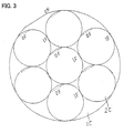
- Fig. 3 is a schematic end view concerning a third embodiment similar to the second embodiment of the present invention, illustrating a process of manufacturing single-crystal semiconductor blocks of a 2-inch diameter from a single-crystal semiconductor block of a 6-inch diameter. This process of manufacturing can also be carried out similarly as in the first and second embodiments described above.
- a single-crystal compound semiconductor ingot of a 6-inch diameter (actually, the diameter is slightly larger than 6 inches for including a grinding allowance), and then its outer periphery is ground and an OF is formed thereon.
- a single-crystal semiconductor block of a 6-inch diameter 1 c whose outer periphery has been ground can then be cut by wire electric discharge machining similarly as in the first and second embodiments to provide seven single-crystal semiconductor blocks 2c of a 2-inch diameter.
- a single process of growing a 6-inch diameter ingot and a single process of slicing the ingot can provide seven times as many 2-inch diameter single-crystal semiconductor blocks as in the case of growing a 2-inch diameter ingot, similarly as in the second embodiment.
- each of single-crystal semiconductor blocks of a 2-inch diameter is cut out having an OF and an IF.
- Such an OF and an IF of each of small-diameter single-crystal semiconductor blocks 2c can be formed during cutting out those small-diameter blocks by wire electric discharge machining, with reference to an OF of large-diameter single-crystal semiconductor block 1c, for example.
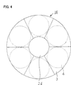
- Fig. 4 is a schematic end face view concerning a fourth embodiment similar to the third embodiment according to the present invention, illustrating a process of manufacturing single-crystal semiconductor blocks of a 2-inch diameter from a single-crystal semiconductor block of a 6-inch diameter.
- a small-diameter single-crystal semiconductor block 2d is cut out including the central part of an end face of a large-scale single-crystal semiconductor block 1d, by wire electric discharge machining similarly as in the third embodiment.
- the remaining thick-walled cylindrical single-crystal block is cut by a band saw to provide six single-crystal blocks 3 each having a sector-shaped end face.
- the band saw can achieve a much higher cutting rate as compared with the wire electric discharge machining.
- single-crystal blocks 3 each having a sector-shaped end face have their peripheries ground to be made into small-diameter single-crystal cylindrical semiconductor blocks 4 of a 2-inch diameter. Accordingly, seven small-diameter single-crystal semiconductor blocks in total can efficiently be obtained from one large-diameter single-crystal semiconductor block.
- a wire electric discharge machining method and a band saw method are described as a method of cutting out small-diameter single-crystal semiconductor blocks from a large-diameter single-crystal semiconductor block, it is also possible to use for electric discharge machining a thin-walled cylindrical discharging electrode having a peripheral shape corresponding to the shape of a small-diameter single-crystal semiconductor block to be cut out.
- the various cutting method described above may be conveniently combined.
- a large-scale single-crystal compound semiconductor block to be cut out has a 6-inch diameter at most at present, it goes without saying that the present invention can be applied to a single-crystal semiconductor block having a larger diameter of 8 inches or 12 inches which will be manufactured in the future.
- small-scale single-crystal semiconductor blocks to be cut out have a 2-inch diameter in the aforementioned embodiments
- the present invention can be used even in the case that a large-diameter single-crystal semiconductor block to be manufactured in the future is cut into small-scale single-crystal semiconductor blocks having a diameter of 3 inches or more (for example, a 9-inch diameter single-crystal semiconductor block can be cut to provide seven 3-inch diameter single-crystal semiconductor blocks).
- small-scale single-crystal semiconductor blocks to be cut out from a large-scale single-crystal semiconductor block are not required to have the same diameter.
- the electrical properties of small-diameter single-crystal semiconductor blocks cut out from a large-diameter single-crystal semiconductor block are not concentrically symmetric except for those cut out from the central part of the large-diameter single-crystal semiconductor block.
Landscapes
- Engineering & Computer Science (AREA)
- Chemical & Material Sciences (AREA)
- Mechanical Engineering (AREA)
- Crystallography & Structural Chemistry (AREA)
- Materials Engineering (AREA)
- Metallurgy (AREA)
- Organic Chemistry (AREA)
- Mining & Mineral Resources (AREA)
- Crystals, And After-Treatments Of Crystals (AREA)
- Mechanical Treatment Of Semiconductor (AREA)
- Processing Of Stones Or Stones Resemblance Materials (AREA)
Abstract
Description
- The present invention relates to a method of manufacturing single-crystal semiconductor blocks, and in particular, to a method of efficiently producing at low costs single-crystal semiconductor blocks for slicing off wafers of a relatively small diameter therefrom.
- At present, various types of semiconductor devices are manufactured from single-crystal semiconductor wafers. To improve the production efficiency of the semiconductor devices, there is generally a need to manufacture the semiconductor devices by using single-crystal semiconductor wafers of a diameter as large as possible. Due to such a need, in the case of silicon, a cylindrical single-crystal ingot of a diameter as large as 12 inches (approximately 30 cm) is grown and then sliced by a slicer, a multiwire saw or the like to thereby produce single-crystal silicon wafers of a 12-inch diameter.
- In the case of a compound semiconductor such as a III-V group compound or a II-VI group compound, it is much more difficult to grow a large-diameter single-crystal ingot as compared with in the case of silicon. Conventionally, therefore, single-crystal compound semiconductor ingots of a 2-inch diameter have mainly been grown and cut to provide single-crystal compound semiconductor wafers of a 2-inch diameter to be used for manufacturing semiconductor devices.
- The technique of growing single-crystal compound semiconductor ingots has been improved in recent years. In some types of compound semiconductors, it is possible to grow a single-crystal ingot having a relatively large diameter of 5 inches (approximately 12.7 cm) or 6 inches (approximately 15.8 cm), for example.
- As described above, however, industrially available single-crystal compound semiconductor wafers conventionally have a 2-inch diameter in the main. Therefore, production lines on which single-crystal compound semiconductor wafers are used to manufacture semiconductor devices have conventionally been constructed suitably for the 2-inch wafers. At present, there still exist a large number of such production lines and they are still in operation. Therefore, even if it is possible to grow single-crystal compound semiconductor ingots having a relatively large diameter of 5 inches or 6 inches, for example, the existing production lines still have a demand for single-crystal compound semiconductor wafers having a 2-inch diameter.
- Under the circumstances described above, even if a semiconductor wafer provider has a technique of growing single-crystal compound semiconductor ingots having a 5-inch or 6-inch diameter, for example, the provider specially grows single-crystal ingots having a 2-inch diameter to meet the demand for 2-inch diameter wafers. Then, the provider grinds the outer periphery of the ingot, and the grinding includes a process of forming an orientation flat (OF) and, if desired, an index flat (IF) too for indicating a crystal orientation. A notch may be formed instead of the OF and IF. Furthermore, the provider slices the single-crystal semiconductor block and polishes the obtained slices to produce target 2-inch diameter wafers.
- As a matter of course, in order to obtain a total wafer area equal to that provided by large-scale wafers of a 5-inch or 6-inch diameter by using small-scale wafers of a 2-inch diameter, several times number of the small-scale wafers are required as compared with the number of the large-scale wafers. To provide such many small-scale wafers, it is necessary to grow many small-diameter ingots.
- This means that a large number of single-crystal growth furnaces are required, which is undesirable in terms of costs and efficiency of wafer production. In such a situation, it may be possible to grow a plurality of small-diameter single-crystal ingots in a large furnace in which a large-diameter single-crystal ingot can be grown. In such a large furnace, however, it is difficult to uniformly adjust growth conditions of a plurality of small-diameter single-crystal ingots, and thus it is difficult to obtain at one time a plurality of small-diameter single-crystal ingots having a uniform and preferable crystal quality.
- In view of such circumstances of the conventional art, an object of the present invention is to provide a method of efficiently manufacturing at low costs single-crystal semiconductor blocks for slicing off wafers of a relatively small diameter desired by users.
- A method of manufacturing single-crystal semiconductor blocks according to the present invention is characterized in that single-crystal semiconductor blocks of a relatively small diameter for slicing off single-crystal semiconductor wafers of a relatively small diameter desired by users are cut out from a single-crystal semiconductor block of a relatively large diameter. Such a method is particularly preferable in the case that the semiconductor is a III-V group compound semiconductor.
- The large-diameter single-crystal semiconductor block to be cut preferably has a thickness of at least 10 mm. The small-diameter single-crystal semiconductor blocks can be cut out by any of an electric discharge machining method, a wire saw method, a grinding method by means of a cylindrical core on which diamond is electrically deposited, and a band saw method. In particular, the electric discharge machining method and the wire saw method, which enable easy cutting along both straight and curved lines in a fully-controlled manner, are preferable because these methods can be used to easily form OFs and IFs by setting an XY-driving stage control device.
- In the cutting process, at least four small-scale single-crystal semiconductor blocks having a diameter of at least 2 inches can be provided from one large-scale single-crystal semiconductor block having a diameter of at least 5 inches. For efficient use of crystal blocks, a total cross-sectional area of a plurality of small-diameter single-crystal semiconductor blocks cut out from one large-diameter single-crystal semiconductor block preferably corresponds to at least 50% of a cross-sectional area of the large-diameter block. On the other hand, when defective parts included in any cross-sectional area of a large-diameter single-crystal semiconductor block (twin-crystals, polycrystals, crystal slips, chips, cracks or the like) correspond to at most 65% of the cross-sectional area of the large-diameter block, small-diameter single-crystal semiconductor blocks can be cut out from the remaining part of the large-diameter block.
- Each of the small-diameter single-crystal semiconductor blocks may be cut out to have any of an orientation flat, an index flat, and a notch for easy determination of its crystal orientation.
- According to the present invention, there can be provided a method of efficiently manufacturing at low costs single-crystal semiconductor blocks of a relatively small diameter desired by users from a single-crystal semiconductor block of a relatively large diameter.
-
- Fig. 1 is a schematic end face view showing how a single-crystal semiconductor block of a 5-inch diameter is cut to provide four single-crystal semiconductor blocks of a 2-inch diameter in an embodiment according to the present invention.
- Fig. 2 is a schematic end face view showing how a single-crystal semiconductor block of a 6-inch diameter is cut to provide five single-crystal semiconductor blocks of a 2-inch diameter in another embodiment according to the present invention.
- Fig. 3 is a schematic end face view showing how a single-crystal semiconductor block of a 6-inch diameter is cut to provide seven single-crystal semiconductor blocks of a 2-inch diameter each having an OF and an IF in a further embodiment according to the present invention.
- Fig. 4 is a schematic end face view showing how a single-crystal semiconductor block of a 6-inch diameter is cut to provide seven single-crystal semiconductor blocks of a 2-inch diameter in a further embodiment according to the present invention.
- 1a: single-crystal semiconductor block of a 5-inch diameter; 1b, 1c and 1d: single-crystal semiconductor block of a 6-inch diameter; 2a, 2b and 2c: single-crystal semiconductor block of a 2-inch diameter; 3: single-crystal semiconductor block having a sector-shaped end face; 4: single-crystal semiconductor block of a 2-inch diameter.
- Fig. 1 is a schematic end face view illustrating a process of manufacturing single-crystal semiconductor blocks of a relatively small diameter from a single-crystal semiconductor block of a relatively large diameter in a first embodiment according to the present invention. At present, for a GaAs compound semiconductor for example, it is possible to grow a single-crystal ingot having a relatively large diameter of 5 inches or 6 inches. For an InP compound semiconductor also, it is almost possible to grow a single-crystal ingot having a relatively large diameter.
- In the first embodiment, there is initially grown a single-crystal compound semiconductor ingot of a 5-inch diameter (actually, the diameter is slightly larger than 5 inches for including a grinding allowance), and then its outer periphery is ground and an OF is formed thereon. As shown in Fig. 1, a single-crystal semiconductor block of a 5-inch diameter la whose outer periphery has been ground can then be cut by wire electric discharge machining for example, to provide four single-crystal semiconductor blocks 2a of a 2-inch diameter.
- In the wire electric discharge machining, a large-diameter single-crystal semiconductor block is mounted on an XY-driving stage. While the XY-driving stage is being driven, a wire is moved in its lengthwise direction parallel to the axial direction of the single-crystal block and allowed to discharge electricity, so that small-diameter single-crystal semiconductor blocks can be cut out along its cylindrical surface. The axial length of the large-diameter single-crystal semiconductor block to be cut is not particularly limited, and it is possible to cut the large-diameter block even in the case that it has a length (or thickness) of more than 10 mm. The wire electric discharge machining requires cutting allowance of approximately at most several hundreds µm, which can reduce the unusable part caused by the cutting allowance in the single crystal.
- According to the embodiment as described above, a single process of growing a 5-inch diameter ingot and a single process of cutting out single-crystal blocks can provide four times as many 2-inch diameter single-crystal semiconductor blocks as in the case of growing a 2-inch diameter ingot.
- Each of the cut-out single-crystal semiconductor blocks of 2-inch diameter has its periphery ground and is provided with an OF, an IF, or a notch. Thereafter, the blocks are sliced to provide 2-inch diameter wafers.
- Fig. 2 is a schematic end face view illustrating a process of manufacturing single-crystal semiconductor blocks of a 2-inch diameter from a single-crystal semiconductor block of a 6-inch diameter in a second embodiment according to the present invention. This process of manufacturing can be carried out similarly as in the first embodiment described above.
- Namely, in the second embodiment, there is initially grown a single-crystal compound semiconductor ingot of a 6-inch diameter (actually, the diameter is slightly larger than 6 inches for including a grinding allowance), and then its outer periphery is ground and an OF is formed thereon. As shown in Fig. 2, a single-
crystal semiconductor block 1b of a 6-inch diameter whose outer periphery has been ground can then be cut by wire electric discharge machining similarly as in the first embodiment to provide five single-crystal semiconductor blocks 2b of a 2-inch diameter. - In other words, a single process of growing a 6-inch diameter ingot and a single process of cutting out crystal blocks can provide five times as many 2-inch diameter single-crystal semiconductor blocks as in the case of growing a 2-inch diameter ingot.
- Fig. 3 is a schematic end view concerning a third embodiment similar to the second embodiment of the present invention, illustrating a process of manufacturing single-crystal semiconductor blocks of a 2-inch diameter from a single-crystal semiconductor block of a 6-inch diameter. This process of manufacturing can also be carried out similarly as in the first and second embodiments described above.
- Namely, in the third embodiment, there is initially grown a single-crystal compound semiconductor ingot of a 6-inch diameter (actually, the diameter is slightly larger than 6 inches for including a grinding allowance), and then its outer periphery is ground and an OF is formed thereon. As shown in Fig. 3, a single-crystal semiconductor block of a 6-inch diameter 1 c whose outer periphery has been ground can then be cut by wire electric discharge machining similarly as in the first and second embodiments to provide seven single-crystal semiconductor blocks 2c of a 2-inch diameter.
- In other words, in the third embodiment, a single process of growing a 6-inch diameter ingot and a single process of slicing the ingot can provide seven times as many 2-inch diameter single-crystal semiconductor blocks as in the case of growing a 2-inch diameter ingot, similarly as in the second embodiment.
- In the third embodiment in Fig. 3, each of single-crystal semiconductor blocks of a 2-inch diameter is cut out having an OF and an IF. Such an OF and an IF of each of small-diameter single-crystal semiconductor blocks 2c can be formed during cutting out those small-diameter blocks by wire electric discharge machining, with reference to an OF of large-diameter single-crystal semiconductor block 1c, for example.
- Fig. 4 is a schematic end face view concerning a fourth embodiment similar to the third embodiment according to the present invention, illustrating a process of manufacturing single-crystal semiconductor blocks of a 2-inch diameter from a single-crystal semiconductor block of a 6-inch diameter. In the fourth embodiment, a small-diameter single-
crystal semiconductor block 2d is cut out including the central part of an end face of a large-scale single-crystal semiconductor block 1d, by wire electric discharge machining similarly as in the third embodiment. - Thereafter, the remaining thick-walled cylindrical single-crystal block is cut by a band saw to provide six single-
crystal blocks 3 each having a sector-shaped end face. The band saw can achieve a much higher cutting rate as compared with the wire electric discharge machining. - Then, single-
crystal blocks 3 each having a sector-shaped end face have their peripheries ground to be made into small-diameter single-crystal cylindrical semiconductor blocks 4 of a 2-inch diameter. Accordingly, seven small-diameter single-crystal semiconductor blocks in total can efficiently be obtained from one large-diameter single-crystal semiconductor block. - Although several embodiments according to the present invention have been described in the above, it is more difficult to grow a large-diameter single-crystal ingot than to grow a small-scale single-crystal ingot, because various defects including twin crystals, polycrystals, crystal slips and others are more likely to be caused during growing a large-diameter single-crystal ingot than a small-diameter single-crystal one. Conventionally, a large-scale wafer cut out from a part including such a defect cannot be shipped as a product and goes to waste. However, with a method of manufacturing small-diameter single-crystal semiconductor blocks according to the present invention described above, there can be obtained a significant advantage that a large-diameter single-crystal semiconductor block including a defect(s) can be cut into small-diameter single-crystal semiconductor blocks, among which those having been cut out from nondefective parts can be shipped as products.
- In the aforementioned embodiments, although a wire electric discharge machining method and a band saw method are described as a method of cutting out small-diameter single-crystal semiconductor blocks from a large-diameter single-crystal semiconductor block, it is also possible to use for electric discharge machining a thin-walled cylindrical discharging electrode having a peripheral shape corresponding to the shape of a small-diameter single-crystal semiconductor block to be cut out. In addition to these cutting methods, it is further possible to use a wire saw method and a grinding method by means of a cylindrical core on which diamond is electrically deposited. Furthermore, of course, the various cutting method described above may be conveniently combined.
- Although a large-scale single-crystal compound semiconductor block to be cut out has a 6-inch diameter at most at present, it goes without saying that the present invention can be applied to a single-crystal semiconductor block having a larger diameter of 8 inches or 12 inches which will be manufactured in the future. Similarly, although small-scale single-crystal semiconductor blocks to be cut out have a 2-inch diameter in the aforementioned embodiments, it goes without saying that the present invention can be used even in the case that a large-diameter single-crystal semiconductor block to be manufactured in the future is cut into small-scale single-crystal semiconductor blocks having a diameter of 3 inches or more (for example, a 9-inch diameter single-crystal semiconductor block can be cut to provide seven 3-inch diameter single-crystal semiconductor blocks). Moreover, in the present invention, small-scale single-crystal semiconductor blocks to be cut out from a large-scale single-crystal semiconductor block are not required to have the same diameter. For example, it is also possible to cut one large-scale single-crystal semiconductor block to provide a small-scale single-crystal semiconductor block(s) of a 2-inch diameter and one(s) of a 3-inch diameter simultaneously.
- Incidentally, the electrical properties of small-diameter single-crystal semiconductor blocks cut out from a large-diameter single-crystal semiconductor block are not concentrically symmetric except for those cut out from the central part of the large-diameter single-crystal semiconductor block.
- As described above, according to the present invention, it is possible to efficiently provide at low costs single-crystal semiconductor blocks of a relatively small diameter desired by users, by cutting out the same from a single-crystal semiconductor block of a relatively large diameter.
Claims (8)
- A method of manufacturing single-crystal semiconductor blocks, wherein single-crystal semiconductor blocks (2a) of a relatively small diameter for slicing off single-crystal semiconductor wafers of a relatively small diameter desired by users are cut out from a single-crystal semiconductor block (1a) of a relatively large diameter.
- The method of manufacturing single-crystal semiconductor blocks according to claim 1, wherein said semiconductor is a III-V group compound semiconductor.
- The method of manufacturing single-crystal semiconductor blocks according to claim 1, wherein said large-diameter single-crystal semiconductor block has a thickness of at least 10 mm.
- The method of manufacturing single-crystal semiconductor blocks according to claim 1, wherein said small-diameter single-crystal semiconductor blocks are cut out by any of an electric discharge machining method, a wire saw method, a grinding method by means of a cylindrical core, and a band saw method.
- The method of manufacturing single-crystal semiconductor blocks according to claim 1, wherein at least four said small-scale single-crystal semiconductor blocks having a diameter of at least 2 inches are cut out from said large-scale single-crystal semiconductor block having a diameter of at least 5 inches.
- The method of manufacturing single-crystal semiconductor blocks according to claim 1, wherein a total cross-sectional area of a plurality of said small-diameter single-crystal semiconductor blocks cut out from said large-scale single-crystal semiconductor block corresponds to at least 50% of a cross-sectional area of said large-scale single-crystal semiconductor block.
- The method of manufacturing single-crystal semiconductor blocks according to claim 1, wherein defective parts included in any cross-sectional area of said large-diameter single-crystal semiconductor block correspond to at most 65% of said cross-sectional area.
- The method of manufacturing single-crystal semiconductor blocks according to claim 1, wherein each of said small-diameter single-crystal semiconductor blocks is formed to have at least any of an orientation flat, an index flat, and a notch for easy determination of its crystal orientation.
Applications Claiming Priority (2)
| Application Number | Priority Date | Filing Date | Title |
|---|---|---|---|
| JP2003291663A JP2005059354A (en) | 2003-08-11 | 2003-08-11 | Method for producing a single crystal mass for slicing a semiconductor wafer |
| PCT/JP2004/010116 WO2005015626A1 (en) | 2003-08-11 | 2004-07-15 | Method for producing single crystal ingot from which semiconductor wafer is sliced |
Publications (2)
| Publication Number | Publication Date |
|---|---|
| EP1617466A1 true EP1617466A1 (en) | 2006-01-18 |
| EP1617466A4 EP1617466A4 (en) | 2006-10-18 |
Family
ID=34131666
Family Applications (1)
| Application Number | Title | Priority Date | Filing Date |
|---|---|---|---|
| EP04747582A Withdrawn EP1617466A4 (en) | 2003-08-11 | 2004-07-15 | PROCESS FOR PRODUCING A MONOCRYSTALLINE INGOT FROM WHICH A SEMICONDUCTOR WAFER IS CUT IN WAFER |
Country Status (8)
| Country | Link |
|---|---|
| US (1) | US20060194416A1 (en) |
| EP (1) | EP1617466A4 (en) |
| JP (1) | JP2005059354A (en) |
| KR (1) | KR20060037251A (en) |
| CN (1) | CN1795542A (en) |
| CA (1) | CA2521513A1 (en) |
| TW (1) | TW200514674A (en) |
| WO (1) | WO2005015626A1 (en) |
Families Citing this family (5)
| Publication number | Priority date | Publication date | Assignee | Title |
|---|---|---|---|---|
| WO2008092132A1 (en) * | 2007-01-25 | 2008-07-31 | University Of Utah Research Foundation | Systems and methods for recycling semiconductor material removed from a raw semiconductor boule |
| CN102814866B (en) * | 2012-08-31 | 2014-10-29 | 北京京运通科技股份有限公司 | Quasi-monocrystal silicon ingot cutting method and silicon wafer manufacturing method |
| JP6167019B2 (en) * | 2012-11-09 | 2017-07-19 | シチズンファインデバイス株式会社 | Substrate processing method and liquid crystal display panel manufacturing method using the same |
| JP6684603B2 (en) * | 2015-02-09 | 2020-04-22 | 株式会社松崎製作所 | Manufacturing method of recycled semiconductor wafer |
| US11456363B2 (en) * | 2018-02-23 | 2022-09-27 | Sumitomo Electric Industries, Ltd. | Indium phosphide crystal substrate |
Family Cites Families (13)
| Publication number | Priority date | Publication date | Assignee | Title |
|---|---|---|---|---|
| US4343832A (en) * | 1980-10-02 | 1982-08-10 | Motorola, Inc. | Semiconductor devices by laser enhanced diffusion |
| EP0279949A1 (en) * | 1987-02-11 | 1988-08-31 | BBC Brown Boveri AG | Process for manufacturing semiconductor components |
| JP2678416B2 (en) * | 1992-08-28 | 1997-11-17 | 信越化学工業株式会社 | Method and apparatus for manufacturing magnetic recording medium substrate |
| JPH09165289A (en) * | 1995-12-13 | 1997-06-24 | Komatsu Electron Metals Co Ltd | Single crystal ingot holding device and holding method |
| US6203416B1 (en) * | 1998-09-10 | 2001-03-20 | Atock Co., Ltd. | Outer-diameter blade, inner-diameter blade, core drill and processing machines using same ones |
| JP2000332078A (en) * | 1999-05-20 | 2000-11-30 | Mitsubishi Materials Silicon Corp | Evaluation method for large diameter wafers |
| JP4808832B2 (en) * | 2000-03-23 | 2011-11-02 | Sumco Techxiv株式会社 | Method for producing defect-free crystals |
| EP1269521A1 (en) * | 2000-04-07 | 2003-01-02 | Varian Semiconductor Equipment Associates Inc. | WAFER ORIENTATION SENSOR FOR GaAs WAFERS |
| JP2002075923A (en) * | 2000-08-28 | 2002-03-15 | Shin Etsu Handotai Co Ltd | Processing method of silicon single crystal ingot |
| US6780239B2 (en) * | 2000-10-19 | 2004-08-24 | Ricoh Company, Ltd. | Crystal growth method, crystal growth apparatus, group-III nitride crystal and group-III nitride semiconductor device |
| JP2004039808A (en) * | 2002-07-02 | 2004-02-05 | Denso Corp | Method and apparatus for manufacturing semiconductor substrate |
| JP4411837B2 (en) * | 2002-12-05 | 2010-02-10 | 株式会社デンソー | Semiconductor substrate manufacturing method and manufacturing apparatus |
| US6890836B2 (en) * | 2003-05-23 | 2005-05-10 | Texas Instruments Incorporated | Scribe street width reduction by deep trench and shallow saw cut |
-
2003
- 2003-08-11 JP JP2003291663A patent/JP2005059354A/en active Pending
-
2004
- 2004-07-15 CA CA002521513A patent/CA2521513A1/en not_active Abandoned
- 2004-07-15 CN CNA2004800143372A patent/CN1795542A/en active Pending
- 2004-07-15 EP EP04747582A patent/EP1617466A4/en not_active Withdrawn
- 2004-07-15 WO PCT/JP2004/010116 patent/WO2005015626A1/en not_active Ceased
- 2004-07-15 US US10/552,275 patent/US20060194416A1/en not_active Abandoned
- 2004-07-15 KR KR1020057021635A patent/KR20060037251A/en not_active Withdrawn
- 2004-07-22 TW TW093121907A patent/TW200514674A/en unknown
Also Published As
| Publication number | Publication date |
|---|---|
| CN1795542A (en) | 2006-06-28 |
| JP2005059354A (en) | 2005-03-10 |
| EP1617466A4 (en) | 2006-10-18 |
| TW200514674A (en) | 2005-05-01 |
| CA2521513A1 (en) | 2005-02-17 |
| WO2005015626A1 (en) | 2005-02-17 |
| KR20060037251A (en) | 2006-05-03 |
| US20060194416A1 (en) | 2006-08-31 |
Similar Documents
| Publication | Publication Date | Title |
|---|---|---|
| CN113423876B (en) | Gallium arsenide single crystal substrate | |
| GB2558395B (en) | Synthesis of thick single crystal diamond material via chemical vapour deposition | |
| JP6513165B2 (en) | Method of manufacturing group III nitride semiconductor single crystal | |
| EP3101160B1 (en) | Semiconductor substrate manufacturing method | |
| JP2001135619A (en) | Silicon focus ring and manufacturing method thereof | |
| EP0221454B1 (en) | Method of producing wafers | |
| JP7518766B2 (en) | Method for processing monocrystalline silicon ingots to improve LLS ring/core pattern | |
| EP3933891A1 (en) | Indium phosphide substrate and method for producing indium phosphide substrate | |
| EP3943645A1 (en) | Sic crystalline substrates with an optimal orientation of lattice planes for fissure reduction and method of producing same | |
| US12195878B2 (en) | SiC crystals with an optimal orientation of lattice planes for fissure reduction and method of producing same | |
| WO2006070556A1 (en) | Epitaxial wafer manufacturing method and epitaxial wafer | |
| US20060194416A1 (en) | Method for producing single crystal ingot from which semiconductor wafer is sliced | |
| EP1583140A1 (en) | Method for producing semiconductor single crystal wafer and laser processing device used therefor | |
| US20030181023A1 (en) | Method of processing silicon single crystal ingot | |
| JP3760187B2 (en) | Processing method of single crystal ingot | |
| JP2005255463A (en) | Sapphire substrate and manufacturing method thereof | |
| JP4949839B2 (en) | Spinel boules, wafers and methods for their production | |
| KR100201705B1 (en) | Mirror Polishing Wafer Manufacturing Method | |
| US6367467B1 (en) | Holding unit for semiconductor wafer sawing | |
| JP4719126B2 (en) | Method for manufacturing silicon carbide single crystal substrate | |
| JP2009051678A (en) | Method for manufacturing sapphire substrate | |
| RU2186887C2 (en) | Method of treatment of grown ingots of silicon single- crystals | |
| CN120772693B (en) | Processing method of edge high-stress hard and brittle semiconductor material | |
| JP2016074553A (en) | Method for producing group III nitride semiconductor single crystal substrate | |
| JPH07117043A (en) | Method for forming semiconductor substrate |
Legal Events
| Date | Code | Title | Description |
|---|---|---|---|
| PUAI | Public reference made under article 153(3) epc to a published international application that has entered the european phase |
Free format text: ORIGINAL CODE: 0009012 |
|
| 17P | Request for examination filed |
Effective date: 20051024 |
|
| AK | Designated contracting states |
Kind code of ref document: A1 Designated state(s): AT BE BG CH CY CZ DE DK EE ES FI FR GB GR HU IE IT LI LU MC NL PL PT RO SE SI SK TR |
|
| AX | Request for extension of the european patent |
Extension state: AL HR LT LV MK |
|
| A4 | Supplementary search report drawn up and despatched |
Effective date: 20060914 |
|
| DAX | Request for extension of the european patent (deleted) | ||
| RBV | Designated contracting states (corrected) |
Designated state(s): DE FR GB |
|
| STAA | Information on the status of an ep patent application or granted ep patent |
Free format text: STATUS: THE APPLICATION IS DEEMED TO BE WITHDRAWN |
|
| 18D | Application deemed to be withdrawn |
Effective date: 20060719 |