EP1617465A1 - Cmp polishing method and method for manufacturing semiconductor device - Google Patents
Cmp polishing method and method for manufacturing semiconductor device Download PDFInfo
- Publication number
- EP1617465A1 EP1617465A1 EP04727407A EP04727407A EP1617465A1 EP 1617465 A1 EP1617465 A1 EP 1617465A1 EP 04727407 A EP04727407 A EP 04727407A EP 04727407 A EP04727407 A EP 04727407A EP 1617465 A1 EP1617465 A1 EP 1617465A1
- Authority
- EP
- European Patent Office
- Prior art keywords
- polishing
- wafer substrate
- less
- polishing pad
- cmp
- Prior art date
- Legal status (The legal status is an assumption and is not a legal conclusion. Google has not performed a legal analysis and makes no representation as to the accuracy of the status listed.)
- Ceased
Links
Images


Classifications
-
- H—ELECTRICITY
- H10—SEMICONDUCTOR DEVICES; ELECTRIC SOLID-STATE DEVICES NOT OTHERWISE PROVIDED FOR
- H10P—GENERIC PROCESSES OR APPARATUS FOR THE MANUFACTURE OR TREATMENT OF DEVICES COVERED BY CLASS H10
- H10P52/00—Grinding, lapping or polishing of wafers, substrates or parts of devices
-
- H—ELECTRICITY
- H10—SEMICONDUCTOR DEVICES; ELECTRIC SOLID-STATE DEVICES NOT OTHERWISE PROVIDED FOR
- H10P—GENERIC PROCESSES OR APPARATUS FOR THE MANUFACTURE OR TREATMENT OF DEVICES COVERED BY CLASS H10
- H10P52/00—Grinding, lapping or polishing of wafers, substrates or parts of devices
- H10P52/40—Chemomechanical polishing [CMP]
- H10P52/403—Chemomechanical polishing [CMP] of conductive or resistive materials
-
- H—ELECTRICITY
- H10—SEMICONDUCTOR DEVICES; ELECTRIC SOLID-STATE DEVICES NOT OTHERWISE PROVIDED FOR
- H10P—GENERIC PROCESSES OR APPARATUS FOR THE MANUFACTURE OR TREATMENT OF DEVICES COVERED BY CLASS H10
- H10P95/00—Generic processes or apparatus for manufacture or treatments not covered by the other groups of this subclass
- H10P95/06—Planarisation of inorganic insulating materials
- H10P95/062—Planarisation of inorganic insulating materials involving a dielectric removal step
Definitions
- the present invention relates to a method for polishing a wafer substrate on which a wiring pattern is formed between materials having a dielectric constant of 2 or less by means of CMP polishing, and a semiconductor device manufacturing method using this method.
- CMP polishing technology (chemical mechanical polishing or chemical mechanical planarization) has been put to practical use as a high-precision flattening technique for meeting such demand.
- FIG. 11 is a head part that causes rotation while holding a wafer substrate 12 which constitutes the object of polishing; this head part has a rotational driving mechanism 13.
- a rotating platen 15 to which a polishing pad 14 is pasted and a rotational driving mechanism 16 for this platen 15 are present facing this head part 11.
- the polishing pad 14, rotating platen 15 and rotational driving mechanism 16 are subjected to swinging by a rotational swinging arm 17, and are also driven in the vertical direction.
- the wafer substrate 12 and polishing pad 14 are caused to rotate at a high speed, and the rotational swinging arm 17 is lowered by a vertical driving mechanism (not shown in the figure), so that pressure is applied to the wafer substrate 12 by the polishing pad 14. Then, a slurry constituting the polishing agent is supplied between the polishing pad 14 and wafer substrate 12. Furthermore, the rotational swinging arm 17 is caused to swing as indicated by the broken line arrow by means of a swinging driving mechanism (not shown in the figure). Then, as a result of the relative rotation and swinging of the polishing pad 14 and wafer substrate 12, the wafer substrate 12 is polished, and the surface is flattened. Specifically, the mechanical polishing caused by the relative motion of the polishing pad 14 and wafer substrate 12 and the chemical polishing caused by the slurry act synergistically, so that favorable polishing is performed.
- the line width of the patterns required in semiconductor devices is becoming increasingly finer, and patterns with a line width of approximately 50 nm have recently been put to a practical use.
- the wiring delay determined by the product of the electrical resistance (R) of the wiring patterns and the capacitance (C) of an insulator is increased by the delay in the semiconductor device; as a result, a problem arises in that the benefits of the increase in speed by the miniaturization cannot be obtained.
- insulators with a dielectric constant of 2 or less (ultra-low-k) have been used.
- the dielectric constant of SiO 2 constituting the insulator formed on a wafer substrate is approximately 3.9 to 4.5, which is significantly greater. Therefore, a method for making SiO 2 porous has been used as a method for lowering the dielectric constant while using SiO 2 as an insulator.
- the present invention was devised in light of such circumstances, and the object of the present invention is to provide a method for performing favorable polishing even in cases where a ultra-low-k material, whose dielectric constant is 2 or less, especially a porous material, is used as the insulating material, and also to provide a semiconductor device manufacturing method using this polishing method.
- the first invention that is used to achieve the object described above is a CMP polishing method, wherein a wafer substrate having a wiring pattern formed between materials with a dielectric constant of 2 or less is polished with the polishing pressure being set at 0.01 to 0.2 psi.
- the second invention that is used to achieve the object described above is the first invention, wherein polishing is performed with the polishing pressure being set at 0.01 to 0.1 psi.
- the third invention that is used to achieve the object described above is the first invention or second invention, wherein the materials with a dielectric constant of 2 or less are porous insulating materials, and the wafer substrate is polished using a polishing pad having a diameter smaller than that of the wafer substrate in a state in which the macroscopic flatness of the surface of the polishing pad is maintained at 5 ⁇ m or less, and the macroscopic flatness of the surface of the wafer substrate is maintained at 3 ⁇ m or less.
- the inventor discovered that with such fragile materials, it is an essential condition to maintain both the macroscopic flatness of the surface of the polishing pad and the macroscopic flatness of the wafer substrate constituting the object of polishing at a specified value or less, which was not much of an issue in conventional CMP apparatuses.
- the macroscopic flatness does not refer to minute irregularity, but rather refers to the difference between the maximum value and the minimum value in the height of the surface in a case where such minute irregularity is seen on an average.
- the reason for requiring such a measure is not always clear; however, it is considered that if the flatness is poor, the pressure does not act uniformly during polishing.
- favorable polishing cannot be performed unless the macroscopic flatness of the surface of the polishing pad is 5 ⁇ m or less, and the macroscopic flatness of the surface of the wafer substrate is 3 ⁇ m or less.
- the polishing pressure needs to be set at 0.01 to 0.2 psi under such a condition. If the polishing pressure is less than 0.01 psi, it becomes difficult to uniformly control the pressure during polishing. Furthermore, if the polishing pressure exceeds 0.2 psi, stripping is generated in the insulating material, so that favorable polishing cannot be performed. This pressure range is significantly low, unlike the range that was conventionally used. It is especially desirable that the polishing pressure be set at 0.1 psi or less.
- the fourth invention that is used to achieve the object described above is the third invention, wherein polishing is performed with the relative velocity between the polishing pad and wafer substrate being set at 6.5 m/sec or lower.
- Equation (1) The Preston equation shown in Equation (1) is widely known as an equation that determines the amount of polishing of the object of polishing.
- Amount of polishing ] k ⁇ V ⁇ P ⁇ t
- k is a constant
- V is the relative velocity of the polishing body and object of polishing
- P is the pressure at which the object of polishing is pressed against the polishing body
- t is the polishing time.
- the polishing pressure P is reduced, the amount of polishing is reduced, so that the required polishing time is increased.
- this relative velocity V is increased beyond a certain level, the slurry that is present between the polishing pad and wafer substrate causes hydroplaning phenomenon, so that the amount of polishing becomes saturated. Therefore, it is meaningless to increase the relative velocity V any higher than this level.
- the relative velocity between the polishing pad and wafer substrate is restricted to 6.5 m/sec or lower on the basis of the experimental results.
- polishing is performed at such a low polishing pressure as that described above, and the polishing speed is to be increased to a level that causes the saturation of the amount of polishing due to the hydroplaning phenomenon as described above, then the polishing rate varies according to the location of the wafer substrate, so that uniform polishing cannot be obtained. Accordingly, it is preferable to suppress the actual relative velocity between the polishing pad and wafer substrate to an even lower level.
- the inventor discovered that as long as the relative velocity between the polishing pad and wafer substrate is 6.5 m/sec or lower, variation in the polishing rate presents no practical problem. Furthermore, if the polishing rate is excessively low, the polishing time is increased; therefore, it is desirable that the relative velocity between the polishing pad and wafer substrate be set at 3.0 m/sec or higher.
- the fifth invention that is used to achieve the object described above is a semiconductor device manufacturing method, wherein this method has a step of polishing the wafer substrate by means of the CMP polishing method according to any of the first through fourth inventions.
- the method since the method has a step of polishing the wafer substrate by means of the CMP polishing method according to one of the first through fourth inventions, the wafer substrate having a ultra-low-k insulating material can be polished in a favorable manner. Consequently, it is possible to manufacture, with a good yield, semiconductor devices having high-density patterns with a very fine line width.
- CMP polishing is performed on a wafer substrate which has a diameter of 300 mm and on one surface of which 25-mm-square IC regions are formed, with each of the IC regions having a pattern with a 0.1- ⁇ m line and space formed thereon.
- the lines are formed from Cu, and the portions of the space are formed from porous SiO 2 having a dielectric constant of 2 or less.
- the polishing pad consists of an IC1000 (commercial name) by Rodel, Inc., and a doughnut type pad is used which has a diameter of 266 mm and in which a hole with a diameter of 84 mm is formed in the central portion.
- PL7102 (commercial name) by Fujimi Incorporated is used as the slurry, with a supply of 150 ml/min.
- the rpm of the wafer substrate is 251 rpm, with this rotation oriented in the opposite direction from the direction of rotation of the polishing pad, and the oscillation velocity of the polishing pad is set at 40 mm/sec.
- the oscillation range is in a range of 30 to 80 mm from the center of the wafer substrate.
- Figure 1 is a diagram showing the relationship between the rotational speed (rpm) of the polishing pad, the polishing speed (relative velocity of the polishing pad and wafer substrate), and the polishing rate.
- the polishing pressure in this case is 0.01 psi.
- the polishing speed As the rpm of the polishing pad increases, the polishing speed also increases, so that the polishing rate is also increased.
- the polishing speed reaches 6.5 m/sec (rpm of the polishing pad: 550 rpm)
- the polishing rate reaches saturation. This is due to hydroplaning phenomenon.
- the polishing speed also varies according to the position of oscillation of the polishing pad, average values are used.
- Figure 2 is a diagram showing the distribution of the polishing rate in the direction of the radius of the wafer substrate, with this distribution investigated under the same conditions as in Figure 1 and with the rotational speed (rpm) of the polishing pad taken as a parameter. It is seen from this diagram that there is almost no difference in the polishing rate between the case where the rpm of the polishing head is 551 rpm and the case where this rpm is 601 rpm, and that when the rpm of the polishing pad reaches 550 rpm or greater as described above, i.e., when the polishing speed reaches 6.5 m/sec or greater, the polishing rate becomes saturated.
- Figure 3 is a diagram showing another experimental data indicating the polishing rate in the direction of the radius of the wafer substrate in a case where the rpm of the polishing pad is set at 301 rpm, i.e., the polishing speed is set at 4.4 m/sec, under the same conditions as described above. It is seen that substantially uniform polishing rates are obtained over the entire region of the wafer substrate.
- Polishing is performed using a similar method with the polishing pressure being changed to 0.05 psi and to 0.1 psi but with the other conditions being the same; there is no crushing, stripping, or the like of the ultra-low-k porous insulating material, so that favorable polishing is performed.
- the polishing pressure is set at a pressure that exceeds 0.2 psi, crushing of the insulating material is generated, and the state of polishing deteriorates.
- FIG. 4 is a flow chart showing a semiconductor device manufacturing process constituting a working configuration of the present invention.
- the appropriate treatment process is first selected in step S100 from the following steps S101 through S104. Then, the processing proceeds to one of the steps S101 through S104 in accordance with this selection.
- Step S101 is an oxidation process which oxidizes the surface of the silicon wafer substrate.
- Step S102 is a CVD process in which an insulating film is formed on the surface of the silicon wafer substrate by CVD or the like.
- Step S103 is an electrode formation process in which electrodes are formed on the silicon wafer substrate by a process such as vacuum evaporation.
- Step S104 is an ion injection process in which ions are injected into the silicon wafer substrate.
- step S105 a judgment is made as to whether or not a CMP process is to be performed. In cases where such a process is to be performed, the processing proceeds to the CMP process in step S106. In cases where a CMP process is not to be performed, the processing bypasses step S106.
- the CMP process the flattening of inter-layer insulating films, the formation of a damascene by the polishing of a metal film on the surface of the semiconductor device, and the like are performed using the polishing apparatus that implements the polishing method of the present invention.
- Step S107 is a photolithographic process.
- the coating of the silicon wafer substrate with a resist, the burning of a circuit pattern onto the silicon wafer substrate by exposure using an exposure apparatus, and the development of the exposed silicon wafer substrate, are performed.
- the subsequent step S108 is an etching process in which the portions other than the developed resist image are removed by etching, the resist is then stripped away, and the unnecessary resist following the completion of etching is removed.
- step S109 a judgment is made as to whether or not all of the required processes have been completed. If the processes have not been completed, the processing returns to step S100, and the preceding steps are repeated so that a circuit pattern is formed on the silicon wafer substrate. If it is judged in step S109 that all of the processes have been completed, the processing is ended.
Landscapes
- Mechanical Treatment Of Semiconductor (AREA)
- Finish Polishing, Edge Sharpening, And Grinding By Specific Grinding Devices (AREA)
- Internal Circuitry In Semiconductor Integrated Circuit Devices (AREA)
Abstract
Description
- The present invention relates to a method for polishing a wafer substrate on which a wiring pattern is formed between materials having a dielectric constant of 2 or less by means of CMP polishing, and a semiconductor device manufacturing method using this method.
- As semiconductor integrated circuits have become finer and more highly integrated, the steps of semiconductor manufacturing processes have become more numerous and complex. Consequently, the surfaces of semiconductor devices are not always flat. The presence of steps in the surfaces of semiconductor devices] leads to step breakage in wiring, local increases in resistance, and the like, and may cause wire breakage, a drop in electrical capacity, and the like. Furthermore, in the insulating films, this may lead to a deterioration in the withstand voltage, the occurrence of leakage, or the like.
- Meanwhile, as semiconductor integrated circuits have become finer and more highly integrated, the light source wavelengths in photolithography have become shorter, and the numerical aperture or so-called NA has become larger. As a result, the focal depths of semiconductor exposure apparatuses have become substantially shallower. In order to handle such shallow focal depths, there has been demand for a greater degree of flattening of the surfaces of semiconductor devices than in the past.
- CMP polishing technology (chemical mechanical polishing or chemical mechanical planarization) has been put to practical use as a high-precision flattening technique for meeting such demand.
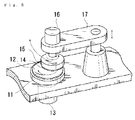
- The basic construction of a CMP apparatus is shown in Figure 5. 11 is a head part that causes rotation while holding a wafer substrate 12 which constitutes the object of polishing; this head part has a
rotational driving mechanism 13. A rotatingplaten 15 to which a polishing pad 14 is pasted and arotational driving mechanism 16 for thisplaten 15 are present facing thishead part 11. The polishing pad 14, rotatingplaten 15 androtational driving mechanism 16 are subjected to swinging by a rotational swingingarm 17, and are also driven in the vertical direction. - When polishing is performed using such a CMP polishing apparatus, the wafer substrate 12 and polishing pad 14 are caused to rotate at a high speed, and the rotational swinging
arm 17 is lowered by a vertical driving mechanism (not shown in the figure), so that pressure is applied to the wafer substrate 12 by the polishing pad 14. Then, a slurry constituting the polishing agent is supplied between the polishing pad 14 and wafer substrate 12. Furthermore, the rotational swingingarm 17 is caused to swing as indicated by the broken line arrow by means of a swinging driving mechanism (not shown in the figure). Then, as a result of the relative rotation and swinging of the polishing pad 14 and wafer substrate 12, the wafer substrate 12 is polished, and the surface is flattened. Specifically, the mechanical polishing caused by the relative motion of the polishing pad 14 and wafer substrate 12 and the chemical polishing caused by the slurry act synergistically, so that favorable polishing is performed. - The line width of the patterns required in semiconductor devices is becoming increasingly finer, and patterns with a line width of approximately 50 nm have recently been put to a practical use. However, when the line width becomes thus finer, the wiring delay determined by the product of the electrical resistance (R) of the wiring patterns and the capacitance (C) of an insulator is increased by the delay in the semiconductor device; as a result, a problem arises in that the benefits of the increase in speed by the miniaturization cannot be obtained. Accordingly, insulators with a dielectric constant of 2 or less (ultra-low-k) have been used. Generally, the dielectric constant of SiO2 constituting the insulator formed on a wafer substrate is approximately 3.9 to 4.5, which is significantly greater. Therefore, a method for making SiO2 porous has been used as a method for lowering the dielectric constant while using SiO2 as an insulator.
- However, if SiO2 is made porous, the mechanical strength is correspondingly weakened, so that the following problem occurs: namely, when CMP polishing is performed, stripping occurs, and favorable polishing cannot be performed. Accordingly, it has been desired to develop a method for polishing a wafer substrate having a ultra-low-k insulating material in a favorable manner.
- The present invention was devised in light of such circumstances, and the object of the present invention is to provide a method for performing favorable polishing even in cases where a ultra-low-k material, whose dielectric constant is 2 or less, especially a porous material, is used as the insulating material, and also to provide a semiconductor device manufacturing method using this polishing method.
- The first invention that is used to achieve the object described above is a CMP polishing method, wherein a wafer substrate having a wiring pattern formed between materials with a dielectric constant of 2 or less is polished with the polishing pressure being set at 0.01 to 0.2 psi.
- The second invention that is used to achieve the object described above is the first invention, wherein polishing is performed with the polishing pressure being set at 0.01 to 0.1 psi.
- The third invention that is used to achieve the object described above is the first invention or second invention, wherein the materials with a dielectric constant of 2 or less are porous insulating materials, and the wafer substrate is polished using a polishing pad having a diameter smaller than that of the wafer substrate in a state in which the macroscopic flatness of the surface of the polishing pad is maintained at 5 µm or less, and the macroscopic flatness of the surface of the wafer substrate is maintained at 3 µm or less.
- As a result of the research conducted on methods for favorably polishing ultra-low-k materials, the inventor discovered that with such fragile materials, it is an essential condition to maintain both the macroscopic flatness of the surface of the polishing pad and the macroscopic flatness of the wafer substrate constituting the object of polishing at a specified value or less, which was not much of an issue in conventional CMP apparatuses. Here, the macroscopic flatness does not refer to minute irregularity, but rather refers to the difference between the maximum value and the minimum value in the height of the surface in a case where such minute irregularity is seen on an average. The reason for requiring such a measure is not always clear; however, it is considered that if the flatness is poor, the pressure does not act uniformly during polishing. Furthermore, it was discovered that favorable polishing cannot be performed unless the macroscopic flatness of the surface of the polishing pad is 5 µm or less, and the macroscopic flatness of the surface of the wafer substrate is 3 µm or less.
- Moreover, it was discovered that the polishing pressure needs to be set at 0.01 to 0.2 psi under such a condition. If the polishing pressure is less than 0.01 psi, it becomes difficult to uniformly control the pressure during polishing. Furthermore, if the polishing pressure exceeds 0.2 psi, stripping is generated in the insulating material, so that favorable polishing cannot be performed. This pressure range is significantly low, unlike the range that was conventionally used. It is especially desirable that the polishing pressure be set at 0.1 psi or less.
- The fourth invention that is used to achieve the object described above is the third invention, wherein polishing is performed with the relative velocity between the polishing pad and wafer substrate being set at 6.5 m/sec or lower.
- The Preston equation shown in Equation (1) is widely known as an equation that determines the amount of polishing of the object of polishing.

- Here, k is a constant, V is the relative velocity of the polishing body and object of polishing, P is the pressure at which the object of polishing is pressed against the polishing body, and t is the polishing time.
- Accordingly, if the polishing pressure P is reduced, the amount of polishing is reduced, so that the required polishing time is increased. In order to prevent this, it is necessary to increase the relative velocity V of the polishing body and the wafer substrate constituting the object of polishing. However, when this relative velocity V is increased beyond a certain level, the slurry that is present between the polishing pad and wafer substrate causes hydroplaning phenomenon, so that the amount of polishing becomes saturated. Therefore, it is meaningless to increase the relative velocity V any higher than this level. Thus, the relative velocity between the polishing pad and wafer substrate is restricted to 6.5 m/sec or lower on the basis of the experimental results.
- Although this was not conventionally known, if polishing is performed at such a low polishing pressure as that described above, and the polishing speed is to be increased to a level that causes the saturation of the amount of polishing due to the hydroplaning phenomenon as described above, then the polishing rate varies according to the location of the wafer substrate, so that uniform polishing cannot be obtained. Accordingly, it is preferable to suppress the actual relative velocity between the polishing pad and wafer substrate to an even lower level. The inventor discovered that as long as the relative velocity between the polishing pad and wafer substrate is 6.5 m/sec or lower, variation in the polishing rate presents no practical problem. Furthermore, if the polishing rate is excessively low, the polishing time is increased; therefore, it is desirable that the relative velocity between the polishing pad and wafer substrate be set at 3.0 m/sec or higher.
- The fifth invention that is used to achieve the object described above is a semiconductor device manufacturing method, wherein this method has a step of polishing the wafer substrate by means of the CMP polishing method according to any of the first through fourth inventions.
- In this invention, since the method has a step of polishing the wafer substrate by means of the CMP polishing method according to one of the first through fourth inventions, the wafer substrate having a ultra-low-k insulating material can be polished in a favorable manner. Consequently, it is possible to manufacture, with a good yield, semiconductor devices having high-density patterns with a very fine line width.
-
- Figure 1 is a diagram showing the relationship between the rotational speed (rpm) of the polishing pad, the polishing speed (relative velocity of the polishing pad and wafer substrate), and the polishing rate in a polishing method constituting an embodiment of the present invention.
- Figure 2 is a diagram showing the distribution of the polishing rate in the direction of the radius of the wafer substrate in a polishing method constituting an embodiment of the present invention with the rotational speed (rpm) of the polishing pad taken as a parameter.
- Figure 3 is a diagram showing another experimental data indicating the polishing rate in the direction of the radius of the wafer substrate in a polishing method constituting an embodiment of the present invention.
- Figure 4 is a flow chart showing a semiconductor device manufacturing process constituting a working configuration of the present invention.
- Figure 5 is a diagram showing the basic construction of a CMP apparatus.
- An embodiment and a working configuration of the present invention will be described below with reference to the figures.
- CMP polishing is performed on a wafer substrate which has a diameter of 300 mm and on one surface of which 25-mm-square IC regions are formed, with each of the IC regions having a pattern with a 0.1-µm line and space formed thereon. The lines are formed from Cu, and the portions of the space are formed from porous SiO2 having a dielectric constant of 2 or less. The polishing pad consists of an IC1000 (commercial name) by Rodel, Inc., and a doughnut type pad is used which has a diameter of 266 mm and in which a hole with a diameter of 84 mm is formed in the central portion. PL7102 (commercial name) by Fujimi Incorporated is used as the slurry, with a supply of 150 ml/min. The rpm of the wafer substrate is 251 rpm, with this rotation oriented in the opposite direction from the direction of rotation of the polishing pad, and the oscillation velocity of the polishing pad is set at 40 mm/sec. The oscillation range is in a range of 30 to 80 mm from the center of the wafer substrate.
- Figure 1 is a diagram showing the relationship between the rotational speed (rpm) of the polishing pad, the polishing speed (relative velocity of the polishing pad and wafer substrate), and the polishing rate. The polishing pressure in this case is 0.01 psi. As the rpm of the polishing pad increases, the polishing speed also increases, so that the polishing rate is also increased. However, when the polishing speed reaches 6.5 m/sec (rpm of the polishing pad: 550 rpm), the polishing rate reaches saturation. This is due to hydroplaning phenomenon. Furthermore, since the polishing speed also varies according to the position of oscillation of the polishing pad, average values are used.
- Figure 2 is a diagram showing the distribution of the polishing rate in the direction of the radius of the wafer substrate, with this distribution investigated under the same conditions as in Figure 1 and with the rotational speed (rpm) of the polishing pad taken as a parameter. It is seen from this diagram that there is almost no difference in the polishing rate between the case where the rpm of the polishing head is 551 rpm and the case where this rpm is 601 rpm, and that when the rpm of the polishing pad reaches 550 rpm or greater as described above, i.e., when the polishing speed reaches 6.5 m/sec or greater, the polishing rate becomes saturated.
- Furthermore, it is seen that even if the polishing rate is lower than that, there is relatively little difference in the polishing rate over the entire wafer substrate up to an rpm of the polishing pad of 401 rpm, but at 451 rpm, which exceeds this rate, the difference in the polishing rate over the entire wafer substrate is increased. When this is seen in correspondence with Figure 1, when the rpm of the polishing pad is 401 rpm (approximately 400 rpm), the polishing speed corresponds to approximately 5.5 m/sec. It is apparent from Figure 2 that as the polishing speed is lower, the polishing rate is generally maintained more uniformly in various portions of the wafer substrate.
- Moreover, in the data range shown in Figure 2, in spite of the fact that ultra-low-k porous SiO2 is used as the insulating material, there is no crushing, stripping, or the like of the insulating material, and it is possible to perform favorable polishing.
- Figure 3 is a diagram showing another experimental data indicating the polishing rate in the direction of the radius of the wafer substrate in a case where the rpm of the polishing pad is set at 301 rpm, i.e., the polishing speed is set at 4.4 m/sec, under the same conditions as described above. It is seen that substantially uniform polishing rates are obtained over the entire region of the wafer substrate.
- Polishing is performed using a similar method with the polishing pressure being changed to 0.05 psi and to 0.1 psi but with the other conditions being the same; there is no crushing, stripping, or the like of the ultra-low-k porous insulating material, so that favorable polishing is performed. However, when the polishing pressure is set at a pressure that exceeds 0.2 psi, crushing of the insulating material is generated, and the state of polishing deteriorates.
- Figure 4 is a flow chart showing a semiconductor device manufacturing process constituting a working configuration of the present invention. When the semiconductor device manufacturing process is started, the appropriate treatment process is first selected in step S100 from the following steps S101 through S104. Then, the processing proceeds to one of the steps S101 through S104 in accordance with this selection.
- Step S101 is an oxidation process which oxidizes the surface of the silicon wafer substrate. Step S102 is a CVD process in which an insulating film is formed on the surface of the silicon wafer substrate by CVD or the like. Step S103 is an electrode formation process in which electrodes are formed on the silicon wafer substrate by a process such as vacuum evaporation. Step S104 is an ion injection process in which ions are injected into the silicon wafer substrate.
- Following the CVD process or electrode formation process, the processing proceeds to step S105. In step S105, a judgment is made as to whether or not a CMP process is to be performed. In cases where such a process is to be performed, the processing proceeds to the CMP process in step S106. In cases where a CMP process is not to be performed, the processing bypasses step S106. In the CMP process, the flattening of inter-layer insulating films, the formation of a damascene by the polishing of a metal film on the surface of the semiconductor device, and the like are performed using the polishing apparatus that implements the polishing method of the present invention.
- Following the CMP process or oxidation process, the processing proceeds to step S107. Step S107 is a photolithographic process. In the photolithographic process, the coating of the silicon wafer substrate with a resist, the burning of a circuit pattern onto the silicon wafer substrate by exposure using an exposure apparatus, and the development of the exposed silicon wafer substrate, are performed. Furthermore, the subsequent step S108 is an etching process in which the portions other than the developed resist image are removed by etching, the resist is then stripped away, and the unnecessary resist following the completion of etching is removed.
- Next, in step S109, a judgment is made as to whether or not all of the required processes have been completed. If the processes have not been completed, the processing returns to step S100, and the preceding steps are repeated so that a circuit pattern is formed on the silicon wafer substrate. If it is judged in step S109 that all of the processes have been completed, the processing is ended.
Claims (7)
- A CMP polishing method, wherein a wafer substrate having a wiring pattern formed between materials with a dielectric constant of 2 or less is polished with the polishing pressure being set at 0.01 to 0.2 psi.
- The CMP polishing method according to Claim 1, wherein polishing is performed with the polishing pressure being set at 0.01 to 0.1 psi.
- The CMP polishing method according to Claim 1, wherein the materials with a dielectric constant of 2 or less are porous insulating materials, and the wafer substrate is polished using a polishing pad having a diameter smaller than that of the wafer substrate in a state in which the macroscopic flatness of the surface of the polishing pad is maintained at 5 µm or less, and the macroscopic flatness of the surface of the wafer substrate is maintained at 3 µm or less.
- The CMP polishing method according to Claim 3, wherein polishing is performed with the relative velocity between the polishing pad and the wafer substrate being set at 6.5 m/sec or lower.
- The CMP polishing method according to Claim 2, wherein the materials with a dielectric constant of 2 or less are porous insulating materials, and the wafer substrate is polished using a polishing pad having a diameter smaller than that of the wafer substrate in a state in which the macroscopic flatness of the surface of the polishing pad is maintained at 5 µm or less, and the macroscopic flatness of the surface of the wafer substrate is maintained at 3 µm or less.
- The CMP polishing method according to Claim 5, wherein polishing is performed with the relative velocity between the polishing pad and the wafer substrate being set at 6.5 m/sec or lower.
- A semiconductor device manufacturing method, wherein this method has a step of polishing the wafer substrate by means of the CMP polishing method according to any one of Claims 1 through 6.
Applications Claiming Priority (2)
| Application Number | Priority Date | Filing Date | Title |
|---|---|---|---|
| JP2003117771A JP2004327566A (en) | 2003-04-23 | 2003-04-23 | CMP polishing method and semiconductor device manufacturing method |
| PCT/JP2004/005310 WO2004095558A1 (en) | 2003-04-23 | 2004-04-14 | Cmp polishing method and method for manufacturing semiconductor device |
Publications (2)
| Publication Number | Publication Date |
|---|---|
| EP1617465A1 true EP1617465A1 (en) | 2006-01-18 |
| EP1617465A4 EP1617465A4 (en) | 2007-07-04 |
Family
ID=33308050
Family Applications (1)
| Application Number | Title | Priority Date | Filing Date |
|---|---|---|---|
| EP04727407A Ceased EP1617465A4 (en) | 2003-04-23 | 2004-04-14 | CHEMICOMECHANICAL POLISHING (CMP) PROCESS AND METHOD OF MANUFACTURING SEMICONDUCTOR DEVICE |
Country Status (7)
| Country | Link |
|---|---|
| US (1) | US20060046491A1 (en) |
| EP (1) | EP1617465A4 (en) |
| JP (1) | JP2004327566A (en) |
| KR (1) | KR20050118667A (en) |
| CN (1) | CN100369212C (en) |
| TW (1) | TW200423245A (en) |
| WO (1) | WO2004095558A1 (en) |
Families Citing this family (2)
| Publication number | Priority date | Publication date | Assignee | Title |
|---|---|---|---|---|
| KR101159658B1 (en) * | 2006-12-28 | 2012-06-25 | 생-고뱅 세라믹스 앤드 플라스틱스, 인코포레이티드 | Method of grinding a sapphire substrate |
| JP2016058724A (en) * | 2014-09-11 | 2016-04-21 | 株式会社荏原製作所 | Processing module, processing apparatus, and processing method |
Family Cites Families (8)
| Publication number | Priority date | Publication date | Assignee | Title |
|---|---|---|---|---|
| JP2000000757A (en) * | 1998-06-12 | 2000-01-07 | Nikon Corp | Polishing apparatus and polishing method |
| US6303507B1 (en) * | 1999-12-13 | 2001-10-16 | Advanced Micro Devices, Inc. | In-situ feedback system for localized CMP thickness control |
| US6475072B1 (en) * | 2000-09-29 | 2002-11-05 | International Business Machines Corporation | Method of wafer smoothing for bonding using chemo-mechanical polishing (CMP) |
| JP4507457B2 (en) * | 2001-05-30 | 2010-07-21 | ソニー株式会社 | Manufacturing method of semiconductor device |
| US6821881B2 (en) * | 2001-07-25 | 2004-11-23 | Applied Materials, Inc. | Method for chemical mechanical polishing of semiconductor substrates |
| JP2003068683A (en) * | 2001-08-22 | 2003-03-07 | Hitachi Chem Co Ltd | Polishing liquid for metal and polishing method |
| JP2003324088A (en) * | 2002-04-30 | 2003-11-14 | Sony Corp | Polishing method and polishing apparatus |
| TWI295950B (en) * | 2002-10-03 | 2008-04-21 | Applied Materials Inc | Method for reducing delamination during chemical mechanical polishing |
-
2003
- 2003-04-23 JP JP2003117771A patent/JP2004327566A/en not_active Withdrawn
-
2004
- 2004-04-14 CN CNB2004800106759A patent/CN100369212C/en not_active Expired - Lifetime
- 2004-04-14 WO PCT/JP2004/005310 patent/WO2004095558A1/en not_active Ceased
- 2004-04-14 KR KR1020057013371A patent/KR20050118667A/en not_active Withdrawn
- 2004-04-14 EP EP04727407A patent/EP1617465A4/en not_active Ceased
- 2004-04-23 TW TW093111382A patent/TW200423245A/en not_active IP Right Cessation
-
2005
- 2005-10-21 US US11/254,732 patent/US20060046491A1/en not_active Abandoned
Also Published As
| Publication number | Publication date |
|---|---|
| TW200423245A (en) | 2004-11-01 |
| EP1617465A4 (en) | 2007-07-04 |
| TWI354326B (en) | 2011-12-11 |
| JP2004327566A (en) | 2004-11-18 |
| US20060046491A1 (en) | 2006-03-02 |
| KR20050118667A (en) | 2005-12-19 |
| WO2004095558A1 (en) | 2004-11-04 |
| CN100369212C (en) | 2008-02-13 |
| CN1777979A (en) | 2006-05-24 |
Similar Documents
| Publication | Publication Date | Title |
|---|---|---|
| US5626715A (en) | Methods of polishing semiconductor substrates | |
| EP0808230B1 (en) | Chemical-mechanical polishing of thin materials using a pulse polishing technique | |
| KR100359552B1 (en) | Combined chemical mechanical polishing and reactive ion etching process | |
| KR100271769B1 (en) | Method for manufacturing semiconductor device, etchant composition and semiconductor device for manufacturing semiconductor device therefor | |
| US20020048959A1 (en) | Diamond as a polish-stop layer for chemical-mechanical planarization in a damascene process flow | |
| KR20000058021A (en) | Chemical mechanical polishing processes and components | |
| KR20000015996A (en) | Chemically-mechanically planarization method of stop-on-feature semiconductor wafer | |
| JP2003514061A (en) | Use of CsOH in dielectric CMP slurry | |
| CN100419963C (en) | Formation of semiconductor structures using a combination of planarization methods and electropolishing | |
| KR20030003061A (en) | Method of manufacturing semiconductor apparatus and solution for polishing the same | |
| US20040253809A1 (en) | Forming a semiconductor structure using a combination of planarizing methods and electropolishing | |
| US6734103B2 (en) | Method of polishing a semiconductor device | |
| US5911111A (en) | Polysilicon polish for patterning improvement | |
| EP1278241A2 (en) | Method for planarizing deposited film | |
| US7731864B2 (en) | Slurry for chemical mechanical polishing of aluminum | |
| US20060046491A1 (en) | CMP polishing method and method for manufacturing semiconductor device | |
| US6114247A (en) | Polishing cloth for use in a CMP process and a surface treatment thereof | |
| US5910022A (en) | Method and system for tungsten chemical mechanical polishing for unplanarized dielectric surfaces | |
| US6899597B2 (en) | Chemical mechanical polishing (CMP) process using fixed abrasive pads | |
| KR100289015B1 (en) | Chemical mechanical polishing method and apparatus | |
| KR100536806B1 (en) | Method for manufacturing semiconductor device | |
| US20040063318A1 (en) | Method of selectively removing metal residues from a dielectric layer by chemical mechanical polishing | |
| KR20000011718A (en) | A method of polishing semiconductor substrate and a method of making semiconductor device | |
| KR20040002285A (en) | Polishing apparatus of semiconductor device and planarization method using the same | |
| JP2005109327A (en) | Wiring formation method |
Legal Events
| Date | Code | Title | Description |
|---|---|---|---|
| PUAI | Public reference made under article 153(3) epc to a published international application that has entered the european phase |
Free format text: ORIGINAL CODE: 0009012 |
|
| 17P | Request for examination filed |
Effective date: 20051018 |
|
| AK | Designated contracting states |
Kind code of ref document: A1 Designated state(s): AT BE BG CH CY CZ DE DK EE ES FI FR GB GR HU IE IT LI LU MC NL PL PT RO SE SI SK TR |
|
| AX | Request for extension of the european patent |
Extension state: AL HR LT LV MK |
|
| DAX | Request for extension of the european patent (deleted) | ||
| RBV | Designated contracting states (corrected) |
Designated state(s): DE FR GB |
|
| RIC1 | Information provided on ipc code assigned before grant |
Ipc: H01L 21/321 20060101ALI20070521BHEP Ipc: H01L 21/3105 20060101AFI20070521BHEP |
|
| A4 | Supplementary search report drawn up and despatched |
Effective date: 20070601 |
|
| 17Q | First examination report despatched |
Effective date: 20070926 |
|
| RAP1 | Party data changed (applicant data changed or rights of an application transferred) |
Owner name: NIKON CORPORATION |
|
| STAA | Information on the status of an ep patent application or granted ep patent |
Free format text: STATUS: THE APPLICATION HAS BEEN REFUSED |
|
| 18R | Application refused |
Effective date: 20101107 |