EP1615196A1 - Method and device for driving a display device with line-wise dynamic addressing - Google Patents
Method and device for driving a display device with line-wise dynamic addressing Download PDFInfo
- Publication number
- EP1615196A1 EP1615196A1 EP04291751A EP04291751A EP1615196A1 EP 1615196 A1 EP1615196 A1 EP 1615196A1 EP 04291751 A EP04291751 A EP 04291751A EP 04291751 A EP04291751 A EP 04291751A EP 1615196 A1 EP1615196 A1 EP 1615196A1
- Authority
- EP
- European Patent Office
- Prior art keywords
- addressing
- data
- line
- speed
- loading
- Prior art date
- Legal status (The legal status is an assumption and is not a legal conclusion. Google has not performed a legal analysis and makes no representation as to the accuracy of the status listed.)
- Withdrawn
Links
Images


Classifications
-
- G—PHYSICS
- G09—EDUCATION; CRYPTOGRAPHY; DISPLAY; ADVERTISING; SEALS
- G09G—ARRANGEMENTS OR CIRCUITS FOR CONTROL OF INDICATING DEVICES USING STATIC MEANS TO PRESENT VARIABLE INFORMATION
- G09G3/00—Control arrangements or circuits, of interest only in connection with visual indicators other than cathode-ray tubes
- G09G3/20—Control arrangements or circuits, of interest only in connection with visual indicators other than cathode-ray tubes for presentation of an assembly of a number of characters, e.g. a page, by composing the assembly by combination of individual elements arranged in a matrix no fixed position being assigned to or needed to be assigned to the individual characters or partial characters
- G09G3/22—Control arrangements or circuits, of interest only in connection with visual indicators other than cathode-ray tubes for presentation of an assembly of a number of characters, e.g. a page, by composing the assembly by combination of individual elements arranged in a matrix no fixed position being assigned to or needed to be assigned to the individual characters or partial characters using controlled light sources
- G09G3/28—Control arrangements or circuits, of interest only in connection with visual indicators other than cathode-ray tubes for presentation of an assembly of a number of characters, e.g. a page, by composing the assembly by combination of individual elements arranged in a matrix no fixed position being assigned to or needed to be assigned to the individual characters or partial characters using controlled light sources using luminous gas-discharge panels, e.g. plasma panels
- G09G3/288—Control arrangements or circuits, of interest only in connection with visual indicators other than cathode-ray tubes for presentation of an assembly of a number of characters, e.g. a page, by composing the assembly by combination of individual elements arranged in a matrix no fixed position being assigned to or needed to be assigned to the individual characters or partial characters using controlled light sources using luminous gas-discharge panels, e.g. plasma panels using AC panels
- G09G3/291—Control arrangements or circuits, of interest only in connection with visual indicators other than cathode-ray tubes for presentation of an assembly of a number of characters, e.g. a page, by composing the assembly by combination of individual elements arranged in a matrix no fixed position being assigned to or needed to be assigned to the individual characters or partial characters using controlled light sources using luminous gas-discharge panels, e.g. plasma panels using AC panels controlling the gas discharge to control a cell condition, e.g. by means of specific pulse shapes
-
- G—PHYSICS
- G09—EDUCATION; CRYPTOGRAPHY; DISPLAY; ADVERTISING; SEALS
- G09G—ARRANGEMENTS OR CIRCUITS FOR CONTROL OF INDICATING DEVICES USING STATIC MEANS TO PRESENT VARIABLE INFORMATION
- G09G3/00—Control arrangements or circuits, of interest only in connection with visual indicators other than cathode-ray tubes
- G09G3/20—Control arrangements or circuits, of interest only in connection with visual indicators other than cathode-ray tubes for presentation of an assembly of a number of characters, e.g. a page, by composing the assembly by combination of individual elements arranged in a matrix no fixed position being assigned to or needed to be assigned to the individual characters or partial characters
- G09G3/22—Control arrangements or circuits, of interest only in connection with visual indicators other than cathode-ray tubes for presentation of an assembly of a number of characters, e.g. a page, by composing the assembly by combination of individual elements arranged in a matrix no fixed position being assigned to or needed to be assigned to the individual characters or partial characters using controlled light sources
- G09G3/28—Control arrangements or circuits, of interest only in connection with visual indicators other than cathode-ray tubes for presentation of an assembly of a number of characters, e.g. a page, by composing the assembly by combination of individual elements arranged in a matrix no fixed position being assigned to or needed to be assigned to the individual characters or partial characters using controlled light sources using luminous gas-discharge panels, e.g. plasma panels
- G09G3/288—Control arrangements or circuits, of interest only in connection with visual indicators other than cathode-ray tubes for presentation of an assembly of a number of characters, e.g. a page, by composing the assembly by combination of individual elements arranged in a matrix no fixed position being assigned to or needed to be assigned to the individual characters or partial characters using controlled light sources using luminous gas-discharge panels, e.g. plasma panels using AC panels
- G09G3/296—Driving circuits for producing the waveforms applied to the driving electrodes
-
- G—PHYSICS
- G09—EDUCATION; CRYPTOGRAPHY; DISPLAY; ADVERTISING; SEALS
- G09G—ARRANGEMENTS OR CIRCUITS FOR CONTROL OF INDICATING DEVICES USING STATIC MEANS TO PRESENT VARIABLE INFORMATION
- G09G3/00—Control arrangements or circuits, of interest only in connection with visual indicators other than cathode-ray tubes
- G09G3/20—Control arrangements or circuits, of interest only in connection with visual indicators other than cathode-ray tubes for presentation of an assembly of a number of characters, e.g. a page, by composing the assembly by combination of individual elements arranged in a matrix no fixed position being assigned to or needed to be assigned to the individual characters or partial characters
- G09G3/22—Control arrangements or circuits, of interest only in connection with visual indicators other than cathode-ray tubes for presentation of an assembly of a number of characters, e.g. a page, by composing the assembly by combination of individual elements arranged in a matrix no fixed position being assigned to or needed to be assigned to the individual characters or partial characters using controlled light sources
- G09G3/28—Control arrangements or circuits, of interest only in connection with visual indicators other than cathode-ray tubes for presentation of an assembly of a number of characters, e.g. a page, by composing the assembly by combination of individual elements arranged in a matrix no fixed position being assigned to or needed to be assigned to the individual characters or partial characters using controlled light sources using luminous gas-discharge panels, e.g. plasma panels
- G09G3/288—Control arrangements or circuits, of interest only in connection with visual indicators other than cathode-ray tubes for presentation of an assembly of a number of characters, e.g. a page, by composing the assembly by combination of individual elements arranged in a matrix no fixed position being assigned to or needed to be assigned to the individual characters or partial characters using controlled light sources using luminous gas-discharge panels, e.g. plasma panels using AC panels
- G09G3/291—Control arrangements or circuits, of interest only in connection with visual indicators other than cathode-ray tubes for presentation of an assembly of a number of characters, e.g. a page, by composing the assembly by combination of individual elements arranged in a matrix no fixed position being assigned to or needed to be assigned to the individual characters or partial characters using controlled light sources using luminous gas-discharge panels, e.g. plasma panels using AC panels controlling the gas discharge to control a cell condition, e.g. by means of specific pulse shapes
- G09G3/293—Control arrangements or circuits, of interest only in connection with visual indicators other than cathode-ray tubes for presentation of an assembly of a number of characters, e.g. a page, by composing the assembly by combination of individual elements arranged in a matrix no fixed position being assigned to or needed to be assigned to the individual characters or partial characters using controlled light sources using luminous gas-discharge panels, e.g. plasma panels using AC panels controlling the gas discharge to control a cell condition, e.g. by means of specific pulse shapes for address discharge
-
- G—PHYSICS
- G09—EDUCATION; CRYPTOGRAPHY; DISPLAY; ADVERTISING; SEALS
- G09G—ARRANGEMENTS OR CIRCUITS FOR CONTROL OF INDICATING DEVICES USING STATIC MEANS TO PRESENT VARIABLE INFORMATION
- G09G2310/00—Command of the display device
- G09G2310/02—Addressing, scanning or driving the display screen or processing steps related thereto
- G09G2310/0202—Addressing of scan or signal lines
- G09G2310/0218—Addressing of scan or signal lines with collection of electrodes in groups for n-dimensional addressing
-
- G—PHYSICS
- G09—EDUCATION; CRYPTOGRAPHY; DISPLAY; ADVERTISING; SEALS
- G09G—ARRANGEMENTS OR CIRCUITS FOR CONTROL OF INDICATING DEVICES USING STATIC MEANS TO PRESENT VARIABLE INFORMATION
- G09G2330/00—Aspects of power supply; Aspects of display protection and defect management
- G09G2330/06—Handling electromagnetic interferences [EMI], covering emitted as well as received electromagnetic radiation
Definitions
- the present invention relates to a method for driving a display device having a plurality of cells or pixels by loading addressing data into a data driver at a loading speed and applying an addressing signal to at least one of said plurality of cells or pixels for an addressing time period corresponding to an addressing speed. Furthermore, the present invention relates to a corresponding device for driving a display device.
- the Plasma technology makes it possible to achieve flat colour panels of large size and with very limited depth without any viewing angle constraints.
- the size of the displays may be much larger than the classical CRT picture tubes.
- a front filter may be applied in front of the panel.
- One goal of this filter is to suppress the EMI (Electro-Magnetic Interference) using the so-called faraday principle: the filter is a transparent layer covered by a thin grid of metal.
- the basic assembly of a screen with a filter is illustrated in Figure 2.
- the panel 1 together with the drivers 2 and the power electronic 3 is arranged in a housing 4 which stops the EMI at the backside of the display device.
- the front filter 5 in front of the panel 1 stops the EMI emitted from the front side of the panel.
- this filter 5 has only a reduced transparency with an actual value between 50% and 60% for consumer applications (for professional applications the norm is not so strict and the transparency is better: 65% to 75%).
- This filtering is really mandatory since if the front filter is removed from a plasma panel, even an IR remote control is not able to work properly. In other words, if the brightness shall be increased as well as the addressing speed also the radiation will be increased, that will require a stronger filter with even less transparency.
- each line electrode (compare Figure 3) of the PDP will be selected one after the other by respective drivers Line Driver 1, Line Driver 2 etc.
- binary data information (cell ON or OFF) will be given on all the data electrodes Y (column electrodes) at one time.
- the column electrodes Y are linked to so-called data drivers Data Driver 1 to Data Driver 27 which act as registers (serial input and parallel output) working at a given data clock (e.g. 40MHz in the present example).
- the line and data drivers are controlled and driven by PDP controller.
- the line electrodes X are arranged on a front plate of a PDP and the column electrodes Y on the back plate.
- 2556 cells have to be written through data drivers.
- the 36 data outputs that are in excess, will not be connected but will be filled up with zeros (OFF) from the plasma control IC.
- Figure 5 shows an example of the overall addressing speed for a primed sub-field.
- the addressing time is lower than 1 ⁇ s per line.
- the addressing time per line increases rapidly.
- the curve of the addressing speed can have different behaviours. All the curves presented here are only examples related to a specific technology. In any case, a characterization of the panel speed should be made specifically for each technology and each new process.
- the object of the present invention is to provide a method and a device for driving a display panel wherein the emitted EMI fulfils the requirement of the respective norms.
- this object is solved by a method for driving a display device having a plurality of cells or pixels by loading addressing data into driving means at a loading speed and applying an addressing signal to at least one of said plurality of cells or pixels for an addressing time period corresponding to an addressing speed on the basis of said addressing data, wherein said loading speed of the addressing data is continuously adaptable to said addressing speed.
- a device for driving a display device having a plurality of cells or pixels including driving means for applying an addressing signal to at least one of said plurality of cells or pixels for an addressing time period corresponding to an addressing speed and controlling means for loading addressing data into said driving means at a loading speed, wherein said controlling means is designed to continuously adapt said loading speed to said addressing speed.
- the major advantage of the present invention is that the loading clock of the data drivers may be matched exactly to the addressing duration. Such different clocking broadens the spectrum of the EMI radiation so that the norm limitations can be fulfilled.
- the loading speed may depend on the presence of a priming signal. Since the addressing speed varies with the presence of the priming signal, also the loading speed will do so.
- the loading speed may vary with the line number of the screen of the display device (e.g. vertical panel behaviour). Specifically, since the addressing speed continuously varies with the line number, also the loading speed changes continuously so that the EMI spectrum is broadened.
- the addressing speed may be changed in dependence on a line number by using a first look up table (LUT).
- LUT look up table
- the loading speed may be changed in dependence on the line number by using a second LUT.
- LUTs enable a simple handling of signal dependencies.
- the main idea of the present invention is to adapt the loading speed precisely to the addressing period.
- a preferred embodiment shall be presented by the way of the example of Figure 5, wherein the sub-fields are primed.
- the first column represents a line to be addressed
- the second column the required speed addressing time per line
- the last one the current data clock to be used at the data driver for the corresponding line.
- the data clock for the case of a primed sub-field is printed over the line number.
- the average frequency is 41,21MHz in this example.
- the maximal clock is 51,50MHz whereas the minimum one is 21,82MHz.
- Figure 10 represents a possible implementation of an apparatus for carrying out the method of the present invention.
- This type of apparatus is already described in PCT application WO 00/46782. It comprises a video degamma circuit 10. RGB data coded with 8 bits are input to this degamma circuit 10. 10 bit-RGB-data output from the video degamma circuit 10 is analyzed on an average power measure block 11 which gives the computed average power value (APL) to a PWE (peak white enhancement) control block 12.
- the control block 12 consults its internal power level mode table located in a LUT 121 and directly generates the selected mode control signals for the other processing blocks. It selects the sustain table to be used and the sub-field encoding (CODING) table to be used in the sub-field coding block 13 which generates 16 bit output data from the 10 bit input data from the video degamma circuit 10.
- CODING sub-field encoding
- the control block 12 also controls the writing of RGB pixel data in a frame memory 14 (WR), the reading of RGB sub-field data from the second frame memory (RD), and the serial to parallel conversion circuit 15 (SP).
- the converted data are output to a PDP 16.
- Two frame memories receiving the 16 bit data from the sub-field coding block 13 are required. Data is written pixelwise, but read sub-field-wise into the conversion circuit 15 (SF-R, SF-G, SF-B). In order to read the complete first sub-field a whole frame must already be present in the memory. In a practical implementation two whole frame memories 14 are present, and while one frame memory is being written, the other is being read, avoiding in this way reading the wrong data. In a cost optimized architecture, the two frame memories 14 are probably located on the same SDRAM memory IC, and access to the two frames is time multiplexed.
- Figure 11 shows the driver part of Figure 10 in detail. Essentially, the structure is the same as that of Figure 3.
- the data drivers Data Driver 1, Data Driver 2, ... Data Driver 27 drive the column electrodes Y of the back plate of the PDP and the line drivers Line Driver 1, Line Driver 2 drive the horizontal line electrodes X of the front plate of the PDP.
- the control block 12 generates the SCAN and SUSTAIN pulses required to drive the PDP driver circuits.
- the length of the addressing signal (addressing speed) will be taken from a first LUT 122, preferably stored in the control block 12, and in fact for each line of the panel.
- the information concerning the data driver clock for the data drivers is taken from a second LUT 123 also preferably stored in the control block 12 and used to send the data from serial/parallel conversion 15 and also to control the data driver loading.
- the data drivers are loaded with a variable clock frequency between 21,82 and 51,50 MHz.
Landscapes
- Engineering & Computer Science (AREA)
- Physics & Mathematics (AREA)
- Power Engineering (AREA)
- Plasma & Fusion (AREA)
- Computer Hardware Design (AREA)
- General Physics & Mathematics (AREA)
- Theoretical Computer Science (AREA)
- Control Of Indicators Other Than Cathode Ray Tubes (AREA)
- Control Of Gas Discharge Display Tubes (AREA)
- Transforming Electric Information Into Light Information (AREA)
- Liquid Crystal Display Device Control (AREA)
Abstract
The EMI spectrum of a display device is to comply with respective norms. Therefore, the clock for loading data into data drivers of a display panel is designed to be variable. Consequently, the electromagnetic radiation produced by the loading clock is broadened thereby reducing the peak amplitude. Thus, the limitations of radiation norms can be complied with.
Description
- The present invention relates to a method for driving a display device having a plurality of cells or pixels by loading addressing data into a data driver at a loading speed and applying an addressing signal to at least one of said plurality of cells or pixels for an addressing time period corresponding to an addressing speed. Furthermore, the present invention relates to a corresponding device for driving a display device.
- Today, the Plasma technology makes it possible to achieve flat colour panels of large size and with very limited depth without any viewing angle constraints. The size of the displays may be much larger than the classical CRT picture tubes.
- Referring to the last generation of European TV, a lot of work has been done to improve its picture quality. Consequently, a new technology like the Plasma one has to provide a picture quality as good as or better than the old standard TV technology. In the field of picture quality, the brightness of the screen is of paramount importance.
- However, the electronic parts of the actual plasma technology give rise to electromagnetic radiation. In order to assure the compatibility of PDP (plasma display device) products with other electronic components (VCR, DVD, PC, Mobile phone...), it is necessary to put a filter in front of the screen. Two major sources of radiation exist:
- Sustain frequency (a solution is not subject of the current document)
- Data driving (a solution is presented in the current document)
- For the rest of the document, the case of a standard PDP using 40 MHz data drivers shall be considered in order to simplify the exposition. The selling of such a product requires given norms to be respected in the fields of radiation as shown Figure 1, for the case of data drivers working at 40 MHz and high content screen (cell R, G, B alternately ON and OFF).
- The limit for consumer applications according to the European norm is depicted in the figure (class B norm). One peak linked to the data driver frequency (40 MHz), exceeds the limit of the norm. In order to fulfil the requirements of the norm, a front filter may be applied in front of the panel. One goal of this filter is to suppress the EMI (Electro-Magnetic Interference) using the so-called faraday principle: the filter is a transparent layer covered by a thin grid of metal. The basic assembly of a screen with a filter is illustrated in Figure 2. The
panel 1 together with thedrivers 2 and the power electronic 3 is arranged in ahousing 4 which stops the EMI at the backside of the display device. Thefront filter 5 in front of thepanel 1 stops the EMI emitted from the front side of the panel. - Nevertheless, this
filter 5 has only a reduced transparency with an actual value between 50% and 60% for consumer applications (for professional applications the norm is not so strict and the transparency is better: 65% to 75%). This filtering is really mandatory since if the front filter is removed from a plasma panel, even an IR remote control is not able to work properly. In other words, if the brightness shall be increased as well as the addressing speed also the radiation will be increased, that will require a stronger filter with even less transparency. - For further reducing the EMI related to the data driving it is necessary to know some aspects of PDP data driving.
- In order to activate the plasma cells before lighting a first stage called writing or addressing stage has to be performed. During this stage, each line electrode (compare Figure 3) of the PDP will be selected one after the other by respective
drivers Line Driver 1,Line Driver 2 etc. During each selection, binary data information (cell ON or OFF) will be given on all the data electrodes Y (column electrodes) at one time. To do that, the column electrodes Y are linked to so-called datadrivers Data Driver 1 toData Driver 27 which act as registers (serial input and parallel output) working at a given data clock (e.g. 40MHz in the present example). The line and data drivers are controlled and driven by PDP controller. Furthermore, the line electrodes X are arranged on a front plate of a PDP and the column electrodes Y on the back plate. In the concrete case of a single scan WVGA PDP having a screen with 852 pixels x 480 lines 852 x 3 (R+G+B) = 2556 cells have to be written through data drivers. Today drivers have commonly two parallel inputs and 96 parallel outputs to the column electrodes Y so that 48 clocks are needed to load the driver (48/40 = 1,2 µs). Finally, since 2556/96=26.625, 27 data drivers are required to write all the cells. The 36 data outputs that are in excess, will not be connected but will be filled up with zeros (OFF) from the plasma control IC. - In this connection it has already been proposed to have a jitter in the data clock. This means that various clocks for each cell at each point of time are used. In that case a jitter generator is added on the data driver clock with a kind of random effect. However, one has to guarantee that the overall loading speed will not exceed the expected writing speed. Such appliance of jitter is not very efficient.
- Moreover, according to the
document EP 1 365 382 various addressing time periods per line may be used as shown in Figure 4. The length of the addressing period is different from line to line. Concerning the evolution of the addressing time per line there are three categories of dependency: - A panel homogeneity dependency: this parameter is related to the fact that the panel does not have the same behaviour among the whole screen.
- A dependency of priming efficiency: the priming operation enables a rapid writing but its efficiency could decrease in time (depending on panel technology).
- A dependency of sustain efficiency: the writing operation is directly followed by the sustain operation. Since the efficiency of the writing operation is linked to the capacity effect of the panel, this could change with the delay to the sustain operation.
- In the amount of sub-fields there may be two different categories as already explained in a
previous document EP 1 250 696: - Sub-field preceded by a priming also called primed sub-field (PSF)
- Sub-field not preceded by a priming also called refreshing sub-field (RSF)
- In Figures 5 and 6 two examples of addressing time per PDP lines for the two previous categories of sub-fields are depicted.
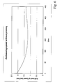
- Figure 5 shows an example of the overall addressing speed for a primed sub-field. In a region around
line 160 the addressing time is lower than 1µs per line. At the large line numbers the addressing time per line increases rapidly. - In contrast to that Figure 6 shows an example of the overall addressing speed for a non-primed sub-field. Although the addressing time is always larger than 1 µs per line it does not essentially increase at the large line numbers.
- Obviously, depending on the panel technology, the curve of the addressing speed can have different behaviours. All the curves presented here are only examples related to a specific technology. In any case, a characterization of the panel speed should be made specifically for each technology and each new process.
- However, according to the technology introduced in
EP 1 365 382 only the addressing speed was changed. In other words, the clock of the data drivers should correspond to the fastest addressing period per line to suit various addressing speeds as disclosed inEP 1 365 382: - In case of Figure 5, the fastest addressing speed is 0.93µs requiring a data driver working at 51,61 MHz.
- In case of Figure 6, the fastest addressing speed is 1.23µs requiring a data driver working at 39,02 MHz.
- Indeed, it is necessary to have the data drivers (compare Figure 3) loaded before writing (i.e. addressing) the line and so the only requirement is to have a loading speed smaller than the addressing period. The loading speed and consequently the data driver clock is kept constant. However, this has a dramatic impact on the EMI as explained in the introduction.
- In view of that the object of the present invention is to provide a method and a device for driving a display panel wherein the emitted EMI fulfils the requirement of the respective norms.
- According to the present invention this object is solved by a method for driving a display device having a plurality of cells or pixels by loading addressing data into driving means at a loading speed and applying an addressing signal to at least one of said plurality of cells or pixels for an addressing time period corresponding to an addressing speed on the basis of said addressing data, wherein said loading speed of the addressing data is continuously adaptable to said addressing speed.
- Furthermore, there is provided a device for driving a display device having a plurality of cells or pixels including driving means for applying an addressing signal to at least one of said plurality of cells or pixels for an addressing time period corresponding to an addressing speed and controlling means for loading addressing data into said driving means at a loading speed, wherein said controlling means is designed to continuously adapt said loading speed to said addressing speed.
- The major advantage of the present invention is that the loading clock of the data drivers may be matched exactly to the addressing duration. Such different clocking broadens the spectrum of the EMI radiation so that the norm limitations can be fulfilled.
- The loading speed may depend on the presence of a priming signal. Since the addressing speed varies with the presence of the priming signal, also the loading speed will do so.
- Thus, the application of a priming signal has to be regarded for controlling the loading speed.
- The loading speed may vary with the line number of the screen of the display device (e.g. vertical panel behaviour). Specifically, since the addressing speed continuously varies with the line number, also the loading speed changes continuously so that the EMI spectrum is broadened.
- The addressing speed may be changed in dependence on a line number by using a first look up table (LUT). Similarly, since the loading speed may be changed in dependence on the line number by using a second LUT. Such LUTs enable a simple handling of signal dependencies.
- Exemplary embodiments of the invention are illustrated in the drawings and are explained in more detail in the following description. The drawings showing in:
- Figure 1
- an EMI radiation and norm limitations;
- Figure 2
- a concept of front filtering against EMI;
- Figure 3
- a block diagram of PDP data driving;
- Figure 4
- a dynamic addressing concept according to the prior art;
- Figure 5
- the addressing speed for a primed sub-field versus the line number;
- Figure 6
- the addressing speed for a non-primed sub-field versus the line number;
- Figure 7
- the clock frequency of a data driver for primed sub-fields according to the present invention;
- Figure 8
- a comparison of EMI spectra for a fixed driver clock and a variable driver clock;
- Figure 9
- an overall EMI spectrum of a PDP according to the present invention;
- Figure 10
- a block diagram of a hardware implementation of an embodiment of the present invention;
- Figure 11
- a block diagram of the data driver according to the present invention.
- The main idea of the present invention is to adapt the loading speed precisely to the addressing period. A preferred embodiment shall be presented by the way of the example of Figure 5, wherein the sub-fields are primed.
- Line 0:
- 1. 35µs ⇒ 35,6MHz
- Line 25:
- 1.23µs ⇒ 39,03MHz
- Line 50:
- 1.13µs ⇒ 42,49MHz
- Line 75:
- 1.05µs⇒ 45,72MHz
- Line 100:
- 0.99µs⇒ 48,49MHz
- Line 125:
- 0.95
µs⇒ 50,54MHz - Line 150:
- 0.93µs⇒ 51,62MHz
- Line 175:
- 0.93µs⇒ 51,62MHz
- Line 200:
- 0.94µs⇒ 51,07MHz
- Line 225:
- 0.97µs⇒ 49,49MHz
- Line 250:
- 1.01µs ⇒ 47,53MHz
- Line 275:
- 1.06µs ⇒ 45,29MHz
- Line 300:
- 1. 14ps ⇒42,11MHz
- Line 325:
- 1.23µs ⇒ 39,03MHz
- Line 350:
- 1.34µs ⇒ 35,83MHz
- Line 375:
- 1.48µs ⇒ 32,43MHz
- Line 400:
- 1.63µs ⇒ 29,45MHz
- Line 425:
- 1.81µs ⇒ 26,51MHz
- Line 480:
- 2.20µs ⇒ 21,82MHz
- In the list, the first column represents a line to be addressed, the second column the required speed addressing time per line and the last one the current data clock to be used at the data driver for the corresponding line. In Figure 7 the data clock for the case of a primed sub-field is printed over the line number. The average frequency is 41,21MHz in this example. The maximal clock is 51,50MHz whereas the minimum one is 21,82MHz.
- The result of the invention on the EMI spectrum is illustrated in Figure 8 wherein the analysis of the radiation is restricted to the data driving. The left half of the figure shows the spectrum for a fixed driver clock, whereas the right half illustrates the broadened spectrum of the varied driver clock.
- The energy emitted by the data driving electronic part did not change but the energy has now been spread on a larger frequency range so that each peak is reduced in amplitude. With such an approach, it will be possible to respect the various norms with a front filter having a better transparency since less energy should now be filtered.
- The overall spectrum of the chosen example is shown in Figure 9. Even in the frequency range below 100 MHz the spectrum clearly lies under the norm limitation symbolized by the dash-dot-line. Thus, the PDP of the present example passes the class B norm.
- Figure 10 represents a possible implementation of an apparatus for carrying out the method of the present invention. This type of apparatus is already described in PCT application WO 00/46782. It comprises a
video degamma circuit 10. RGB data coded with 8 bits are input to thisdegamma circuit 10. 10 bit-RGB-data output from thevideo degamma circuit 10 is analyzed on an averagepower measure block 11 which gives the computed average power value (APL) to a PWE (peak white enhancement)control block 12. One computation can be done as follows:
control block 12 consults its internal power level mode table located in aLUT 121 and directly generates the selected mode control signals for the other processing blocks. It selects the sustain table to be used and the sub-field encoding (CODING) table to be used in thesub-field coding block 13 which generates 16 bit output data from the 10 bit input data from thevideo degamma circuit 10. - The
control block 12 also controls the writing of RGB pixel data in a frame memory 14 (WR), the reading of RGB sub-field data from the second frame memory (RD), and the serial to parallel conversion circuit 15 (SP). The converted data are output to aPDP 16. - Two frame memories receiving the 16 bit data from the
sub-field coding block 13 are required. Data is written pixelwise, but read sub-field-wise into the conversion circuit 15 (SF-R, SF-G, SF-B). In order to read the complete first sub-field a whole frame must already be present in the memory. In a practical implementation twowhole frame memories 14 are present, and while one frame memory is being written, the other is being read, avoiding in this way reading the wrong data. In a cost optimized architecture, the twoframe memories 14 are probably located on the same SDRAM memory IC, and access to the two frames is time multiplexed. - Figure 11 shows the driver part of Figure 10 in detail. Essentially, the structure is the same as that of Figure 3. The data
drivers Data Driver 1,Data Driver 2, ...Data Driver 27 drive the column electrodes Y of the back plate of the PDP and the linedrivers Line Driver 1,Line Driver 2 drive the horizontal line electrodes X of the front plate of the PDP. Finally thecontrol block 12 generates the SCAN and SUSTAIN pulses required to drive the PDP driver circuits., The length of the addressing signal (addressing speed) will be taken from afirst LUT 122, preferably stored in thecontrol block 12, and in fact for each line of the panel. At the same time, the information concerning the data driver clock for the data drivers is taken from asecond LUT 123 also preferably stored in thecontrol block 12 and used to send the data from serial/parallel conversion 15 and also to control the data driver loading. In the present example the data drivers are loaded with a variable clock frequency between 21,82 and 51,50 MHz. - The whole computation of all parameters from such concept will be made one time for a given panel technology and then stored in the PROM or
LUT
Claims (10)
- Method for driving a display device having a plurality of cells or pixels by- loading addressing data into driving means (Data Driver 1 to Data Driver 27) at a loading speed and- applying an addressing signal to at least one of said plurality of cells or pixels for an addressing time period corresponding to an addressing speed on the basis of said addressing data,
characterized in that- said loading speed of the addressing data is continuously adaptable to said addressing speed. - Method according to claim 1, wherein said loading speed depends on the presence of a priming signal.
- Method according to claim 1 or 2, wherein said loading speed is variable with the vertical position of the line on the screen of said display device.
- Method according to one of the preceding claims, wherein said addressing speed is changed in dependence on a line number by using a first LUT (122).
- Method according to one of the preceding claims, wherein said loading speed is changed in dependence on a line number by using a second LUT (123).
- Device for driving a display device (16) having a plurality of cells or pixels including- driving means (Data Driver 1 to Data Driver 27) for applying an addressing signal to at least one of said plurality of cells or pixels for an addressing time period corresponding to an addressing speed and- controlling means (12) for loading addressing data into said driving means (Data Driver 1 to Data Driver 27) at a loading speed ,
characterized in that- said controlling means (12) is designed to continuously adapt said loading speed to said addressing speed. - Device according to claim 6, wherein said loading speed is controllable by said controlling means (12) in dependence of the presence of a priming signal.
- Device according to claim 6 or 7, wherein said loading speed is variable by said controlling means (12) in dependence on the vertical position of the line on the screen of said display device (16).
- Device according to one of the claims 6 to 8, wherein said controlling means (12) includes first memory means for a first LUT (122) for changing said addressing speed in dependence on a line number.
- Device according to one of the claims 6 to 9, wherein said controlling means (12) includes second memory means for a second LUT (123) for changing said loading speed in dependence on a line number.
Priority Applications (7)
| Application Number | Priority Date | Filing Date | Title |
|---|---|---|---|
| EP04291751A EP1615196A1 (en) | 2004-07-09 | 2004-07-09 | Method and device for driving a display device with line-wise dynamic addressing |
| EP05105568A EP1615200A3 (en) | 2004-07-09 | 2005-06-22 | Method and device for driving a display device with line-wise dynamic addressing |
| MXPA05007363A MXPA05007363A (en) | 2004-07-09 | 2005-07-07 | Method and device for driving a display device with line-wise dynamic addressing. |
| US11/177,276 US8780092B2 (en) | 2004-07-09 | 2005-07-08 | Method and device for driving a display device with line-wise dynamic addressing |
| JP2005200653A JP5243688B2 (en) | 2004-07-09 | 2005-07-08 | Method and apparatus for driving display device by line-wise dynamic addressing |
| KR1020050061725A KR101135103B1 (en) | 2004-07-09 | 2005-07-08 | Method and device for driving a display device with line-wise dynamic addressing |
| CNB2005100825791A CN100517438C (en) | 2004-07-09 | 2005-07-11 | Method and device for driving a display device with line-wise dynamic addressing |
Applications Claiming Priority (1)
| Application Number | Priority Date | Filing Date | Title |
|---|---|---|---|
| EP04291751A EP1615196A1 (en) | 2004-07-09 | 2004-07-09 | Method and device for driving a display device with line-wise dynamic addressing |
Publications (1)
| Publication Number | Publication Date |
|---|---|
| EP1615196A1 true EP1615196A1 (en) | 2006-01-11 |
Family
ID=34931237
Family Applications (1)
| Application Number | Title | Priority Date | Filing Date |
|---|---|---|---|
| EP04291751A Withdrawn EP1615196A1 (en) | 2004-07-09 | 2004-07-09 | Method and device for driving a display device with line-wise dynamic addressing |
Country Status (6)
| Country | Link |
|---|---|
| US (1) | US8780092B2 (en) |
| EP (1) | EP1615196A1 (en) |
| JP (1) | JP5243688B2 (en) |
| KR (1) | KR101135103B1 (en) |
| CN (1) | CN100517438C (en) |
| MX (1) | MXPA05007363A (en) |
Families Citing this family (1)
| Publication number | Priority date | Publication date | Assignee | Title |
|---|---|---|---|---|
| KR101404545B1 (en) * | 2007-07-05 | 2014-06-09 | 삼성디스플레이 주식회사 | Driving apparatus and method for display device and display device including the same |
Citations (4)
| Publication number | Priority date | Publication date | Assignee | Title |
|---|---|---|---|---|
| US6175194B1 (en) * | 1999-02-19 | 2001-01-16 | Pioneer Corporation | Method for driving a plasma display panel |
| EP1139324A2 (en) * | 2000-03-31 | 2001-10-04 | Fujitsu Limited | Display apparatus with reduced noise emission and driving method for the display apparatus |
| US20020044118A1 (en) * | 2000-08-29 | 2002-04-18 | Fujitsu Limited | Liquid crystal display apparatus and reduction of electromagnetic interference |
| EP1271463A2 (en) * | 2001-06-22 | 2003-01-02 | Pioneer Corporation | Method of driving plasma display panel |
Family Cites Families (19)
| Publication number | Priority date | Publication date | Assignee | Title |
|---|---|---|---|---|
| JP2737697B2 (en) * | 1995-05-26 | 1998-04-08 | 日本電気株式会社 | Driving method of gas discharge display panel |
| JP3408684B2 (en) | 1995-12-25 | 2003-05-19 | 富士通株式会社 | Driving method of plasma display panel and plasma display device |
| US6057809A (en) * | 1996-08-21 | 2000-05-02 | Neomagic Corp. | Modulation of line-select times of individual rows of a flat-panel display for gray-scaling |
| US5757338A (en) * | 1996-08-21 | 1998-05-26 | Neomagic Corp. | EMI reduction for a flat-panel display controller using horizontal-line based spread spectrum |
| JP4163787B2 (en) | 1997-06-20 | 2008-10-08 | 株式会社大宇エレクトロニクス | Apparatus and method for timing control of AC plasma display flat plate apparatus |
| JPH11352917A (en) | 1998-06-10 | 1999-12-24 | Mitsubishi Electric Corp | Display device and display driving method |
| EP1026655A1 (en) * | 1999-02-01 | 2000-08-09 | Deutsche Thomson-Brandt Gmbh | Method for power level control of a display device and apparatus for carrying out the method |
| JP3708754B2 (en) | 1999-06-01 | 2005-10-19 | パイオニア株式会社 | Driving device for plasma display panel |
| JP3939066B2 (en) | 2000-03-08 | 2007-06-27 | 富士通日立プラズマディスプレイ株式会社 | Color plasma display device |
| JP2002182612A (en) | 2000-12-11 | 2002-06-26 | Sony Corp | Image display device |
| JP4151258B2 (en) | 2001-11-06 | 2008-09-17 | 松下電器産業株式会社 | Plasma display device |
| JP3658362B2 (en) | 2001-11-08 | 2005-06-08 | キヤノン株式会社 | Video display device and control method thereof |
| JP3724430B2 (en) | 2002-02-04 | 2005-12-07 | ソニー株式会社 | Organic EL display device and control method thereof |
| EP1365382A1 (en) * | 2002-05-22 | 2003-11-26 | Thomson Licensing S.A. | Method of driving a plasma display panel |
| EP1365378A1 (en) * | 2002-05-22 | 2003-11-26 | Deutsche Thomson-Brandt Gmbh | Method for driving plasma display panel |
| JP2004061702A (en) | 2002-07-26 | 2004-02-26 | Matsushita Electric Ind Co Ltd | Plasma display device |
| JP4415533B2 (en) | 2002-09-26 | 2010-02-17 | ソニー株式会社 | Plasma display device and driving method thereof |
| JP4423848B2 (en) | 2002-10-31 | 2010-03-03 | ソニー株式会社 | Image display device and color balance adjustment method thereof |
| JP2005070488A (en) | 2003-08-26 | 2005-03-17 | Matsushita Electric Ind Co Ltd | Ac type plasma display device and its driving method |
-
2004
- 2004-07-09 EP EP04291751A patent/EP1615196A1/en not_active Withdrawn
-
2005
- 2005-07-07 MX MXPA05007363A patent/MXPA05007363A/en not_active Application Discontinuation
- 2005-07-08 JP JP2005200653A patent/JP5243688B2/en not_active Expired - Fee Related
- 2005-07-08 KR KR1020050061725A patent/KR101135103B1/en not_active IP Right Cessation
- 2005-07-08 US US11/177,276 patent/US8780092B2/en not_active Expired - Fee Related
- 2005-07-11 CN CNB2005100825791A patent/CN100517438C/en not_active Expired - Fee Related
Patent Citations (4)
| Publication number | Priority date | Publication date | Assignee | Title |
|---|---|---|---|---|
| US6175194B1 (en) * | 1999-02-19 | 2001-01-16 | Pioneer Corporation | Method for driving a plasma display panel |
| EP1139324A2 (en) * | 2000-03-31 | 2001-10-04 | Fujitsu Limited | Display apparatus with reduced noise emission and driving method for the display apparatus |
| US20020044118A1 (en) * | 2000-08-29 | 2002-04-18 | Fujitsu Limited | Liquid crystal display apparatus and reduction of electromagnetic interference |
| EP1271463A2 (en) * | 2001-06-22 | 2003-01-02 | Pioneer Corporation | Method of driving plasma display panel |
Also Published As
| Publication number | Publication date |
|---|---|
| CN100517438C (en) | 2009-07-22 |
| KR101135103B1 (en) | 2012-04-16 |
| KR20060049991A (en) | 2006-05-19 |
| CN1719498A (en) | 2006-01-11 |
| JP2006023751A (en) | 2006-01-26 |
| US8780092B2 (en) | 2014-07-15 |
| JP5243688B2 (en) | 2013-07-24 |
| US20060034144A1 (en) | 2006-02-16 |
| MXPA05007363A (en) | 2006-01-20 |
Similar Documents
| Publication | Publication Date | Title |
|---|---|---|
| EP1256924B1 (en) | Method and apparatus for processing video pictures | |
| US7164415B2 (en) | Display controller and display device provided therewith | |
| US7602365B2 (en) | Display device | |
| US7173580B2 (en) | Method for optimizing brightness in a display device and apparatus for implementing the method | |
| KR100898668B1 (en) | Method and apparatus for controlling a display device | |
| JP5675030B2 (en) | Method for processing video image displayed on display device | |
| US20020018032A1 (en) | Method for controlling light emission of a matrix display in a display period and apparatus for carrying out the method | |
| KR100746059B1 (en) | Pdp data driver, pdp driving method, plasma display device, and control method for the same | |
| CN100454992C (en) | Method for processing video image displayed on display device | |
| US8780092B2 (en) | Method and device for driving a display device with line-wise dynamic addressing | |
| JPH07248744A (en) | Method of driving plasma display | |
| US20050093777A1 (en) | Panel driving apparatus | |
| EP1615200A2 (en) | Method and device for driving a display device with line-wise dynamic addressing | |
| KR20040079943A (en) | Method of an apparatus for driving a plasma display panel | |
| EP1437706A2 (en) | Method for optimizing brightness in a display device and apparatus for implementing the method | |
| JP2002140031A (en) | Driving device for display device, and display device | |
| US7019716B2 (en) | Driving method for PDPs with variable vertical frequency | |
| EP1365382A1 (en) | Method of driving a plasma display panel | |
| KR100531097B1 (en) | Device for driving plasma display panel and method thereof | |
| KR100280887B1 (en) | Driving device of plasma display panel | |
| CN100373431C (en) | Addressing method and device of plasma display device | |
| KR100531096B1 (en) | Device for driving plasma display panel and method thereof | |
| KR100266324B1 (en) | A generation of data load clock for pdp television | |
| KR20050044091A (en) | Discharge display apparatus having improved operation sequence | |
| KR20040050976A (en) | Driving method for decreasing address period in plasma display panel |
Legal Events
| Date | Code | Title | Description |
|---|---|---|---|
| PUAI | Public reference made under article 153(3) epc to a published international application that has entered the european phase |
Free format text: ORIGINAL CODE: 0009012 |
|
| AK | Designated contracting states |
Kind code of ref document: A1 Designated state(s): AT BE BG CH CY CZ DE DK EE ES FI FR GB GR HU IE IT LI LU MC NL PL PT RO SE SI SK TR |
|
| AX | Request for extension of the european patent |
Extension state: AL HR LT LV MK |
|
| AKX | Designation fees paid | ||
| REG | Reference to a national code |
Ref country code: DE Ref legal event code: 8566 |
|
| STAA | Information on the status of an ep patent application or granted ep patent |
Free format text: STATUS: THE APPLICATION IS DEEMED TO BE WITHDRAWN |
|
| 18D | Application deemed to be withdrawn |
Effective date: 20060712 |