EP1612971A1 - Method and apparatus for optical signal transmission - Google Patents
Method and apparatus for optical signal transmission Download PDFInfo
- Publication number
- EP1612971A1 EP1612971A1 EP05253819A EP05253819A EP1612971A1 EP 1612971 A1 EP1612971 A1 EP 1612971A1 EP 05253819 A EP05253819 A EP 05253819A EP 05253819 A EP05253819 A EP 05253819A EP 1612971 A1 EP1612971 A1 EP 1612971A1
- Authority
- EP
- European Patent Office
- Prior art keywords
- signals
- transmission link
- modulator
- duobinary
- signal
- Prior art date
- Legal status (The legal status is an assumption and is not a legal conclusion. Google has not performed a legal analysis and makes no representation as to the accuracy of the status listed.)
- Granted
Links
- 230000003287 optical effect Effects 0.000 title claims abstract description 47
- 238000000034 method Methods 0.000 title claims abstract description 11
- 230000008054 signal transmission Effects 0.000 title abstract description 20
- 230000005540 biological transmission Effects 0.000 claims abstract description 71
- 239000006185 dispersion Substances 0.000 claims abstract description 48
- 238000012544 monitoring process Methods 0.000 claims description 4
- 230000009977 dual effect Effects 0.000 claims description 3
- 238000010586 diagram Methods 0.000 description 11
- 238000004088 simulation Methods 0.000 description 8
- 238000001914 filtration Methods 0.000 description 7
- 230000000295 complement effect Effects 0.000 description 3
- 239000000835 fiber Substances 0.000 description 3
- 238000002474 experimental method Methods 0.000 description 2
- 230000007274 generation of a signal involved in cell-cell signaling Effects 0.000 description 2
- 230000009022 nonlinear effect Effects 0.000 description 2
- 230000010287 polarization Effects 0.000 description 2
- -1 Dlink Substances 0.000 description 1
- 238000013459 approach Methods 0.000 description 1
- 230000006735 deficit Effects 0.000 description 1
- 230000001934 delay Effects 0.000 description 1
- 238000012986 modification Methods 0.000 description 1
- 230000004048 modification Effects 0.000 description 1
- 230000005693 optoelectronics Effects 0.000 description 1
- 230000002269 spontaneous effect Effects 0.000 description 1
Images



Classifications
-
- H—ELECTRICITY
- H04—ELECTRIC COMMUNICATION TECHNIQUE
- H04B—TRANSMISSION
- H04B10/00—Transmission systems employing electromagnetic waves other than radio-waves, e.g. infrared, visible or ultraviolet light, or employing corpuscular radiation, e.g. quantum communication
- H04B10/50—Transmitters
- H04B10/501—Structural aspects
- H04B10/503—Laser transmitters
- H04B10/505—Laser transmitters using external modulation
- H04B10/5055—Laser transmitters using external modulation using a pre-coder
-
- H—ELECTRICITY
- H04—ELECTRIC COMMUNICATION TECHNIQUE
- H04B—TRANSMISSION
- H04B10/00—Transmission systems employing electromagnetic waves other than radio-waves, e.g. infrared, visible or ultraviolet light, or employing corpuscular radiation, e.g. quantum communication
- H04B10/25—Arrangements specific to fibre transmission
- H04B10/2507—Arrangements specific to fibre transmission for the reduction or elimination of distortion or dispersion
- H04B10/2513—Arrangements specific to fibre transmission for the reduction or elimination of distortion or dispersion due to chromatic dispersion
- H04B10/25137—Arrangements specific to fibre transmission for the reduction or elimination of distortion or dispersion due to chromatic dispersion using pulse shaping at the transmitter, e.g. pre-chirping or dispersion supported transmission [DST]
-
- H—ELECTRICITY
- H04—ELECTRIC COMMUNICATION TECHNIQUE
- H04B—TRANSMISSION
- H04B10/00—Transmission systems employing electromagnetic waves other than radio-waves, e.g. infrared, visible or ultraviolet light, or employing corpuscular radiation, e.g. quantum communication
- H04B10/25—Arrangements specific to fibre transmission
- H04B10/2507—Arrangements specific to fibre transmission for the reduction or elimination of distortion or dispersion
- H04B10/2543—Arrangements specific to fibre transmission for the reduction or elimination of distortion or dispersion due to fibre non-linearities, e.g. Kerr effect
-
- H—ELECTRICITY
- H04—ELECTRIC COMMUNICATION TECHNIQUE
- H04B—TRANSMISSION
- H04B10/00—Transmission systems employing electromagnetic waves other than radio-waves, e.g. infrared, visible or ultraviolet light, or employing corpuscular radiation, e.g. quantum communication
- H04B10/25—Arrangements specific to fibre transmission
- H04B10/2507—Arrangements specific to fibre transmission for the reduction or elimination of distortion or dispersion
- H04B10/2572—Arrangements specific to fibre transmission for the reduction or elimination of distortion or dispersion due to forms of polarisation-dependent distortion other than PMD
-
- H—ELECTRICITY
- H04—ELECTRIC COMMUNICATION TECHNIQUE
- H04B—TRANSMISSION
- H04B10/00—Transmission systems employing electromagnetic waves other than radio-waves, e.g. infrared, visible or ultraviolet light, or employing corpuscular radiation, e.g. quantum communication
- H04B10/50—Transmitters
- H04B10/501—Structural aspects
- H04B10/503—Laser transmitters
- H04B10/505—Laser transmitters using external modulation
-
- H—ELECTRICITY
- H04—ELECTRIC COMMUNICATION TECHNIQUE
- H04B—TRANSMISSION
- H04B10/00—Transmission systems employing electromagnetic waves other than radio-waves, e.g. infrared, visible or ultraviolet light, or employing corpuscular radiation, e.g. quantum communication
- H04B10/50—Transmitters
- H04B10/501—Structural aspects
- H04B10/503—Laser transmitters
- H04B10/505—Laser transmitters using external modulation
- H04B10/5057—Laser transmitters using external modulation using a feedback signal generated by analysing the optical output
- H04B10/50575—Laser transmitters using external modulation using a feedback signal generated by analysing the optical output to control the modulator DC bias
-
- H—ELECTRICITY
- H04—ELECTRIC COMMUNICATION TECHNIQUE
- H04B—TRANSMISSION
- H04B10/00—Transmission systems employing electromagnetic waves other than radio-waves, e.g. infrared, visible or ultraviolet light, or employing corpuscular radiation, e.g. quantum communication
- H04B10/50—Transmitters
- H04B10/516—Details of coding or modulation
- H04B10/5167—Duo-binary; Alternative mark inversion; Phase shaped binary transmission
Definitions
- the present invention relates generally to optical transmission and more particularly to methods and apparatus for generating transmitting optical signals.
- Duobinary is a well-known modulation format in fiber optic communications.
- Optical duobinary signals typically have two to three times the chromatic dispersion tolerance of conventional binary signals as well as a high tolerance to nonlinear penalties.
- the increased chromatic dispersion tolerance of duobinary transmission can provide significant cost savings in optical transmission systems by removing the need for dispersion compensation modules (DCMs).
- DCMs dispersion compensation modules
- One technique for realizing transmission of optical duobinary signals is to generate a three-level modulator drive signal by filtering a differentially encoded binary NRZ data stream with an electrical low-pass filter.
- the filtered drive signal drives a modulator to generate the duobinary signals for transmission across a transmission link to a receiver.
- This technique is typically referred to as the electrical low-pass filtered (LPF) duobinary approach.
- LPF electrical low-pass filtered
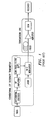
- FIG. 1 An example of an optical transmission system for transmitting electrical LPF duobinary signals is shown in FIG. 1.
- the differential encoder shown in FIG. 1 is used to pre-code the data before the low-pass filtering so that the generated optical duobinary signal (after digitization at the receiver) is the same as the original data.
- Duobinary transmission systems are potentially cost effective commercial fiber optic transport solutions, particularly for metropolitan applications.
- transmission links with low chromatic dispersion e.g. chromatic dispersion compensated links or links spanning relatively short distances
- back-to-back transmission duobinary signals can suffer a 2 - 4 dB optical signal-to-noise (OSNR) penalty as compared to conventional binary signals.
- OSNR optical signal-to-noise
- duobinary signals also referred to hereinafter as duobinary signals
- ASE amplified spontaneous emission
- duobinary signals have higher tolerance to amplified spontaneous emission (ASE) noise as compared to conventional binary signals when the transmission link has a chromatic dispersion above an identifiable dispersion threshold
- an inverse-data signal has higher tolerance to ASE noise as compared to duobinary signals when the transmission link has a chromatic dispersion below the dispersion threshold.
- duobinary signals perform poorly when the chromatic dispersion of a transmission link is low or when there is no chromatic dispersion in the transmission link.
- transmission of inverse-data signals in accordance with the invention can be used to provide high tolerance to ASE noise.
- inverse-data signal' refers to a signal having a complementary intensity profile or waveform to that of a duobinary signal. Additionally, inverse-data signals have a data content that is inverted as compared to the data content of a duobinary signal.
- apparatus and methods are provided to adaptively generate either a duobinary signal or an inverse-data signal, depending on the chromatic dispersion of a transmission link in order to optimize the transmission performance across the transmission link.
- switching between duobinary signal generation and inverse-data signal generation is achieved by controlling the bias of a modulator used to generate the signals.
- switching between transmission of a duobinary -signal and an inverse-data signal is achieved using an optical 1x2 switch to switch between transmission of such signals from complementary output ports of a dual output modulator.
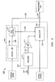
- an apparatus 200 for transmitting optical signals includes a transmitter 210 and bias control apparatus 260.
- the transmitter 210 preferably includes a precoder 215, an amplifier 217 and a modulator 220.
- the precoder 215 preferably comprises a differential encoder and is used to convert a data signal 201 into a differentially encoded drive signal 216.
- the drive signal 216 is used to drive the modulator 220 to produce an optical signal 225 for transmission across a transmission link.
- the modulator 220 is preferably a Mach-Zehnder modulator arranged to encode the data from the drive signal 216 onto light from an optical source to generate the optical signal 225.
- the amplifier 217 is preferably an RF amplifier and is provided to amplify the drive signal 216 prior to driving the modulator 220.
- the amplifier 217 is needed only if the power output from the precoder 215 is not sufficient to drive the modulator 220.
- the amplifier 217 can be removed entirely from the transmitter 210 architecture if the power of the drive signal 216 output from the precoder 215 is sufficient to drive the modulator 220.
- a low-pass filter (not shown) may be included in the transmitter 210 to provide low-pass filtering of the drive signal 216 to generate low-pass filtered duobinary and inverse-data signals.
- the modulator 220 may be selected such that the modulator 220 limits the frequency response of the transmitter 210 and provides the low-pass filtering for generation of optical duobinary and inverse-data signals.
- a bias control apparatus 260 is coupled to the transmitter 210 to control the bias of the modulator 220.
- the bias control apparatus 260 preferably includes a control unit 265 and a bias control 267.
- the control unit 265 receives information from a network device (e.g. a network controller) such as information regarding the data rate of the transmitter, the transmission link and/or the chromatic dispersion of the transmission link on which the optical signal 225 is to be transmitted.
- Chromatic dispersion of a transmission link refers to the chromatic dispersion accumulated in a transmission link between a transmitter and a receiver.
- the control unit 265 uses the information from the network device to determine whether to vary the bias of the modulator 220 so that a duobinary or inverse-data signal is generated. Based on this determination, the control unit 265 then generates a control signal 266 for controlling the bias control 267.
- the bias control 267 is coupled to the control unit 265 and the modulator 220 to control the bias of the modulator 220 based on the control signal 266. Specifically, the bias control 267 receives the control signal 266 from the control unit 265 and generates a bias voltage 280 that is applied to one arm of the modulator 220 to set, through an electro-optical effect, the optical phase difference between the two waves traveling in the arms of the modulator 220. This allows for switching the generated optical signal 225 output from the modulator 220 between a duobinary signal and an inverse-data signal. Specifically, the bias condition for generating a duobinary signal is achieved by applying a bias voltage 280 that biases the modulator 220 at null. The bias condition for generating an inverse-data signal is achieved by applying a bias voltage 280 that biases the modulator 220 at peak. The bias voltages for null and peak bias conditions differ by V ⁇ .
- the bias control 267 also receives a power monitoring signal 290 from a detector 295 which detects the power of the generated optical signal 225.
- the bias control 267 can then vary the bias voltage signal 280 to maintain a desired bias condition (i.e. null or peak bias) of the modulator 220 based on feedback from the power monitoring signal 290.
- a desired bias condition i.e. null or peak bias
- an appropriate bias control algorithm will be used by the bias control 267 to maintain the desired bias condition.
- bias control 267 is integrated within the transmitter 210, or where the bias control 267 and the detector 295 are integrated with the modulator 220, etc.
- an apparatus for transmitting optical signals 300 across a transmission link includes a transmitter 310 and a controller 360.
- the transmitter 310 preferably includes a precoder 315, an amplifier 317, a modulator 320 and an optical switch 375.
- the precoder 315 preferably comprises a differential encoder and is used to convert a data signal 301 into a differentially encoded drive signal 316.
- the drive signal 316 is used to drive the modulator 320.
- the modulator 320 is preferably a dual output Mach-Zehnder modulator arranged to encode the data from the drive signal 316 onto light from an optical source and generate two complementary outputs: 1) an duobinary signal 325 at a data output port 326, and 2) an inverse-data signal 335 at an inverse-data output port 336.
- the optical switch 375 is coupled to the data output port 326 and the inverse-data output port 336 of the modulator 320, and has an output port 376.
- the controller 360 controls the optical switch 375 to switch between transmission of the duobinary signal 325 and transmission of the inverse-data signal 335 through the output port 376 of the optical switch 375 to the transmission link.
- the controller 360 controls the operation of the of the optical switch 375 based on information received from a network device (e.g. a network controller) such as information regarding the data rate of the transmitter, the transmission link and/or the chromatic dispersion of the transmission link on which either the duobinary signal 325 or the inverse-data signal 335 is to be transmitted. Specifically, the controller 360 determines whether the duobinary signal 325 or the inverse-data signal 335 should be transmitted across the transmission link based on the information received from the network device to substantially optimize transmission performance.
- a network device e.g. a network controller
- the amplifier 317 is preferably an RF amplifier and is provided to amplify the drive signal 316 prior to driving the modulator 320.
- the amplifier 317 is needed only if the power output from the precoder 315 is not sufficient to drive the modulator 320.
- the amplifier 317 can be removed entirely from the transmitter 310 architecture if the power of the drive signal 316 output from the precoder 315 is sufficient to drive the modulator 320.
- a low-pass filter (not shown) may be included in the transmitter 310 to provide low-pass filtering of the drive signal 316 to generate low-pass filtered duobinary and inverse-data signals.
- the modulator 320 may be selected such that the modulator 320 limits the frequency response of the transmitter 310 and provides low-pass filtering for generation of optical signals.
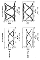
- FIGs. 4 a-f show eye diagrams from a simulation that was performed to compare non-return-to-zero (NRZ) signal transmission, duobinary signal transmission, and inverse-data signal transmission, at 0 km and 40 km.
- the simulation modeled a 10Gb/s optical transmission apparatus having a Mach-Zehnder modulator in accordance with one embodiment of the invention. It is understood, however, that the present invention can be generally applied to optical transmission apparatus for transmission at various bit rates (e.g. 40 Gb/s) by proportionally scaling the bandwidth of the modulator in the transmitter and the bandwidth of the low-pass filter (the bandwidth of the low-pass filter is preferably about 1 ⁇ 4 of the bit rate).
- bit rates e.g. 40 Gb/s
- an inverse-data signal has as wide or wider eye openings near the 0-level (i.e. performs as well or better) than NRZ or duobinary signals in ASE noise-limited cases.
- the OSNR required for a bit error rate of 1 E-3 is ⁇ 10 dB for NRZ signals, ⁇ 13 dB for a duobinary (non-inverted) signals, and ⁇ 10 dB for inverse-data signals.
- the OSNR required for a bit error rate of 1E-3 is ⁇ 12.5 dB for NRZ signals, ⁇ 12 dB for a duobinary (non-inverted) signals, and ⁇ 12 dB for inverse-data signals.
- transmission performance can be improved by up to about 3 dB by using inverse-data signals when the chromatic dispersion of a transmission link is low (i.e. below a dispersion threshold of about 700 ps/nm).
- D link > D th the duobinary signal is selected for transmission; otherwise, the inverse-data signal is selected.
- duobinary signal As discussed above, it has also been found that, by selecting either the duobinary signal or the inverse-data signal (based on the chromatic dispersion of the transmission link), a higher tolerance to timing jitter in the drive signal, PMD, narrow optical filtering, and nonlinear penalties such as self-phase modulation (SPM) and cross-phase modulation (XPM) can be achieved.
- SPM self-phase modulation
- XPM cross-phase modulation
- One reason for the improved tolerance is that the duobinary and inverse-data signals have a wider 0-level (above and below the dispersion threshold, respectively) and are thus more immune to inter-symbol interference.
- FIGs. 5 a-c show eye diagrams from an experiment performed to compare the performance of duobinary and inverse-data signal transmission over 0km, and inverse-data signal transmission after 40km, where significant timing jitter of the modulator drive signal is present.
- the inverse-data signal (after transmission through 0 km and 40 km of SSMF at 10Gb/s) has wider eye opening (at the decision level which is near the 0-level) and thus better performance than the duobinary signal.
- FIGs. 6 a-d show eye diagrams from another simulation performed to compare the polarization mode dispersion tolerance for duobinary and inverse-data signal transmission with zero chromatic dispersion and differential group delays (DGDs) of 0 ps and 40 ps. From the simulation it was found that the OSNR penalty for the inverse-data signal transmission is less than about 1.5 dB with a DGD of 40 ps in a 10.7 Gb/s system, which is more than 1 dB less than that for duobinary signal transmission. Thus, the inverse-data signal has better PMD tolerance when transmitted across transmission links with no chromatic dispersion. It can be understood by those skilled in the art that in transmission links with higher chromatic dispersion (i.e. D link >D th ) the PMD tolerance of duobinary signals is better than that of inverse-data signals.
- D link >D th the PMD tolerance of duobinary signals is better than that of inverse-data signals.
- FIGs. 7 a-c show eye diagrams from a simulation performed to compare the nonlinearity tolerance for NRZ, duobinary and inverse-data signal transmission over a long-distance link (i.e. 2000 km) having low chromatic dispersion but large nonlinear effects such as SPM and XPM.
- a long-distance link i.e. 2000 km
- nonlinear effects such as SPM and XPM.
- the present invention can be implemented using transmitter apparatus and other components comprising discrete components or integrated modules (e.g. transmitters having laser/modulator modules, duobinary driver/modulator modules, laser/duobinary driver/modulator modules, and the like).
- transmitters having laser/modulator modules, duobinary driver/modulator modules, laser/duobinary driver/modulator modules, and the like.
Landscapes
- Physics & Mathematics (AREA)
- Electromagnetism (AREA)
- Engineering & Computer Science (AREA)
- Computer Networks & Wireless Communication (AREA)
- Signal Processing (AREA)
- Optics & Photonics (AREA)
- Nonlinear Science (AREA)
- Optical Communication System (AREA)
- Optical Modulation, Optical Deflection, Nonlinear Optics, Optical Demodulation, Optical Logic Elements (AREA)
Abstract
Description
- This application is related to co-pending patent applications entitled "Apparatus And Method For Duobinary Transmission" and "Duobinary Transmission System and Method" filed January 31, 2003, both of which are incorporated herein by reference.
- The present invention relates generally to optical transmission and more particularly to methods and apparatus for generating transmitting optical signals.
- Duobinary is a well-known modulation format in fiber optic communications. Optical duobinary signals typically have two to three times the chromatic dispersion tolerance of conventional binary signals as well as a high tolerance to nonlinear penalties. The increased chromatic dispersion tolerance of duobinary transmission can provide significant cost savings in optical transmission systems by removing the need for dispersion compensation modules (DCMs).
- One technique for realizing transmission of optical duobinary signals is to generate a three-level modulator drive signal by filtering a differentially encoded binary NRZ data stream with an electrical low-pass filter. The filtered drive signal drives a modulator to generate the duobinary signals for transmission across a transmission link to a receiver. This technique is typically referred to as the electrical low-pass filtered (LPF) duobinary approach. An example of an optical transmission system for transmitting electrical LPF duobinary signals is shown in FIG. 1. The differential encoder shown in FIG. 1 is used to pre-code the data before the low-pass filtering so that the generated optical duobinary signal (after digitization at the receiver) is the same as the original data.
- Duobinary transmission systems are potentially cost effective commercial fiber optic transport solutions, particularly for metropolitan applications. However, in transmission links with low chromatic dispersion (e.g. chromatic dispersion compensated links or links spanning relatively short distances) or with back-to-back transmission, duobinary signals can suffer a 2 - 4 dB optical signal-to-noise (OSNR) penalty as compared to conventional binary signals.
- One aspect of the present invention involves the recognition that conventional optical duobinary signals (also referred to hereinafter as duobinary signals) have higher tolerance to amplified spontaneous emission (ASE) noise as compared to conventional binary signals when the transmission link has a chromatic dispersion above an identifiable dispersion threshold, while an inverse-data signal has higher tolerance to ASE noise as compared to duobinary signals when the transmission link has a chromatic dispersion below the dispersion threshold. Specifically, duobinary signals perform poorly when the chromatic dispersion of a transmission link is low or when there is no chromatic dispersion in the transmission link. In such cases, transmission of inverse-data signals in accordance with the invention can be used to provide high tolerance to ASE noise. (The term 'inverse-data signal', as used herein, refers to a signal having a complementary intensity profile or waveform to that of a duobinary signal. Additionally, inverse-data signals have a data content that is inverted as compared to the data content of a duobinary signal.)
- In another aspect of the present invention it has been recognized that by transmitting inverse-data signals instead of duobinary signals when the chromatic dispersion of a transmission link is below a dispersion threshold, the transmission performance is significantly improved with regard to impairments from timing jitter in the drive signals, polarization-mode dispersion (PMD), and nonlinear effects.
- In preferred embodiments of the present invention, apparatus and methods are provided to adaptively generate either a duobinary signal or an inverse-data signal, depending on the chromatic dispersion of a transmission link in order to optimize the transmission performance across the transmission link.
- In one embodiment of an apparatus according to the invention switching between duobinary signal generation and inverse-data signal generation is achieved by controlling the bias of a modulator used to generate the signals. In an alternative embodiment, switching between transmission of a duobinary -signal and an inverse-data signal is achieved using an optical 1x2 switch to switch between transmission of such signals from complementary output ports of a dual output modulator.
-
- FIG. 1 is a schematic diagram of a prior art electrical LPF duobinary transmitter and transmission link;
- FIG. 2 is a schematic diagram of one embodiment of an apparatus for transmitting optical signals according to the invention;
- FIG. 3 is a schematic diagram of another embodiment of an apparatus for transmitting optical signals according to the invention;
- FIGs. 4 a-f show eye diagrams from a simulation comparing performance of non-return-to-zero (NRZ) signal transmission, duobinary signal transmission, and inverse-data signal transmission, at 0km and 40km;
- FIGs. 5 a-c show eye diagrams from an experiment comparing performance of duobinary and inverse-data signal transmission over 0km, and inverse-data signal transmission after 40km;
- FIGs. 6 a-d show eye diagrams from a simulation comparing polarization mode dispersion tolerance for duobinary and inverse-data signal transmission;
- FIGs. 7 a-c show eye diagrams from a simulation comparing nonlinearity tolerance for NRZ, duobinary, and inverse-data signal transmission.
- In one preferred embodiment of the invention, shown in FIG. 2, an
apparatus 200 for transmitting optical signals is provided. Theapparatus 200 includes atransmitter 210 andbias control apparatus 260. - The
transmitter 210 preferably includes aprecoder 215, anamplifier 217 and amodulator 220. Theprecoder 215 preferably comprises a differential encoder and is used to convert adata signal 201 into a differentially encodeddrive signal 216. Thedrive signal 216 is used to drive themodulator 220 to produce anoptical signal 225 for transmission across a transmission link. - The
modulator 220 is preferably a Mach-Zehnder modulator arranged to encode the data from thedrive signal 216 onto light from an optical source to generate theoptical signal 225. - The
amplifier 217 is preferably an RF amplifier and is provided to amplify thedrive signal 216 prior to driving themodulator 220. Theamplifier 217 is needed only if the power output from theprecoder 215 is not sufficient to drive themodulator 220. Theamplifier 217 can be removed entirely from thetransmitter 210 architecture if the power of thedrive signal 216 output from theprecoder 215 is sufficient to drive themodulator 220. - A low-pass filter (not shown) may be included in the
transmitter 210 to provide low-pass filtering of thedrive signal 216 to generate low-pass filtered duobinary and inverse-data signals. Alternatively, themodulator 220 may be selected such that themodulator 220 limits the frequency response of thetransmitter 210 and provides the low-pass filtering for generation of optical duobinary and inverse-data signals. - A
bias control apparatus 260 is coupled to thetransmitter 210 to control the bias of themodulator 220. Thebias control apparatus 260 preferably includes acontrol unit 265 and abias control 267. Thecontrol unit 265 receives information from a network device (e.g. a network controller) such as information regarding the data rate of the transmitter, the transmission link and/or the chromatic dispersion of the transmission link on which theoptical signal 225 is to be transmitted. (Chromatic dispersion of a transmission link, as used herein, refers to the chromatic dispersion accumulated in a transmission link between a transmitter and a receiver.) Thecontrol unit 265 uses the information from the network device to determine whether to vary the bias of themodulator 220 so that a duobinary or inverse-data signal is generated. Based on this determination, thecontrol unit 265 then generates acontrol signal 266 for controlling thebias control 267. - The
bias control 267 is coupled to thecontrol unit 265 and themodulator 220 to control the bias of themodulator 220 based on thecontrol signal 266. Specifically, thebias control 267 receives thecontrol signal 266 from thecontrol unit 265 and generates abias voltage 280 that is applied to one arm of themodulator 220 to set, through an electro-optical effect, the optical phase difference between the two waves traveling in the arms of themodulator 220. This allows for switching the generatedoptical signal 225 output from themodulator 220 between a duobinary signal and an inverse-data signal. Specifically, the bias condition for generating a duobinary signal is achieved by applying abias voltage 280 that biases themodulator 220 at null. The bias condition for generating an inverse-data signal is achieved by applying abias voltage 280 that biases themodulator 220 at peak. The bias voltages for null and peak bias conditions differ by Vπ. - Preferably, the
bias control 267 also receives apower monitoring signal 290 from adetector 295 which detects the power of the generatedoptical signal 225. Thebias control 267 can then vary thebias voltage signal 280 to maintain a desired bias condition (i.e. null or peak bias) of themodulator 220 based on feedback from thepower monitoring signal 290. Those skilled in the art can appreciate that an appropriate bias control algorithm will be used by thebias control 267 to maintain the desired bias condition. - It will be appreciated by those skilled in the art that various arrangements can be used to practice the invention, such as, where the
bias control 267 is integrated within thetransmitter 210, or where thebias control 267 and thedetector 295 are integrated with themodulator 220, etc. - In another embodiment of the invention, shown in FIG. 3, an apparatus for transmitting
optical signals 300 across a transmission link is provided. Theapparatus 300 includes atransmitter 310 and acontroller 360. Thetransmitter 310 preferably includes aprecoder 315, anamplifier 317, amodulator 320 and anoptical switch 375. Theprecoder 315 preferably comprises a differential encoder and is used to convert a data signal 301 into a differentially encodeddrive signal 316. Thedrive signal 316 is used to drive themodulator 320. - The
modulator 320 is preferably a dual output Mach-Zehnder modulator arranged to encode the data from thedrive signal 316 onto light from an optical source and generate two complementary outputs: 1) anduobinary signal 325 at adata output port 326, and 2) an inverse-data signal 335 at an inverse-data output port 336. - The
optical switch 375 is coupled to thedata output port 326 and the inverse-data output port 336 of themodulator 320, and has anoutput port 376. Thecontroller 360 controls theoptical switch 375 to switch between transmission of theduobinary signal 325 and transmission of the inverse-data signal 335 through theoutput port 376 of theoptical switch 375 to the transmission link. - The
controller 360 controls the operation of the of theoptical switch 375 based on information received from a network device (e.g. a network controller) such as information regarding the data rate of the transmitter, the transmission link and/or the chromatic dispersion of the transmission link on which either theduobinary signal 325 or the inverse-data signal 335 is to be transmitted. Specifically, thecontroller 360 determines whether theduobinary signal 325 or the inverse-data signal 335 should be transmitted across the transmission link based on the information received from the network device to substantially optimize transmission performance. - The
amplifier 317 is preferably an RF amplifier and is provided to amplify thedrive signal 316 prior to driving themodulator 320. Theamplifier 317 is needed only if the power output from theprecoder 315 is not sufficient to drive themodulator 320. Theamplifier 317 can be removed entirely from thetransmitter 310 architecture if the power of thedrive signal 316 output from theprecoder 315 is sufficient to drive themodulator 320. - A low-pass filter (not shown) may be included in the
transmitter 310 to provide low-pass filtering of thedrive signal 316 to generate low-pass filtered duobinary and inverse-data signals. Alternatively, themodulator 320 may be selected such that themodulator 320 limits the frequency response of thetransmitter 310 and provides low-pass filtering for generation of optical signals. - FIGs. 4 a-f show eye diagrams from a simulation that was performed to compare non-return-to-zero (NRZ) signal transmission, duobinary signal transmission, and inverse-data signal transmission, at 0 km and 40 km. The simulation modeled a 10Gb/s optical transmission apparatus having a Mach-Zehnder modulator in accordance with one embodiment of the invention. It is understood, however, that the present invention can be generally applied to optical transmission apparatus for transmission at various bit rates (e.g. 40 Gb/s) by proportionally scaling the bandwidth of the modulator in the transmitter and the bandwidth of the low-pass filter (the bandwidth of the low-pass filter is preferably about ¼ of the bit rate).
- Referring again to FIGs. 4 a-f, those skilled in the art can appreciate that with zero or low chromatic dispersion an inverse-data signal has as wide or wider eye openings near the 0-level (i.e. performs as well or better) than NRZ or duobinary signals in ASE noise-limited cases.
- At 0 km (i.e. back-to-back transmission or transmission over a link with zero dispersion (D=0)), the OSNR required for a bit error rate of 1 E-3 is ~10 dB for NRZ signals, ~13 dB for a duobinary (non-inverted) signals, and ~10 dB for inverse-data signals.
- For transmission over 40 km of standard single mode fiber (SSMF) (corresponding to a chromatic dispersion (D) value of ~680 ps/nm) the OSNR required for a bit error rate of 1E-3 is ~12.5 dB for NRZ signals, ~12 dB for a duobinary (non-inverted) signals, and ~12 dB for inverse-data signals. Thus, transmission performance can be improved by up to about 3 dB by using inverse-data signals when the chromatic dispersion of a transmission link is low (i.e. below a dispersion threshold of about 700 ps/nm).
- The decision to switch between the transmission of a duobinary signal and an inverse-data signal can thus be made by comparing the transmission link dispersion, Dlink, and a dispersion threshold

- As discussed above, it has also been found that, by selecting either the duobinary signal or the inverse-data signal (based on the chromatic dispersion of the transmission link), a higher tolerance to timing jitter in the drive signal, PMD, narrow optical filtering, and nonlinear penalties such as self-phase modulation (SPM) and cross-phase modulation (XPM) can be achieved. One reason for the improved tolerance is that the duobinary and inverse-data signals have a wider 0-level (above and below the dispersion threshold, respectively) and are thus more immune to inter-symbol interference.
- FIGs. 5 a-c show eye diagrams from an experiment performed to compare the performance of duobinary and inverse-data signal transmission over 0km, and inverse-data signal transmission after 40km, where significant timing jitter of the modulator drive signal is present. As can be understood by those skilled in the art, the inverse-data signal (after transmission through 0 km and 40 km of SSMF at 10Gb/s) has wider eye opening (at the decision level which is near the 0-level) and thus better performance than the duobinary signal.
- FIGs. 6 a-d show eye diagrams from another simulation performed to compare the polarization mode dispersion tolerance for duobinary and inverse-data signal transmission with zero chromatic dispersion and differential group delays (DGDs) of 0 ps and 40 ps. From the simulation it was found that the OSNR penalty for the inverse-data signal transmission is less than about 1.5 dB with a DGD of 40 ps in a 10.7 Gb/s system, which is more than 1 dB less than that for duobinary signal transmission. Thus, the inverse-data signal has better PMD tolerance when transmitted across transmission links with no chromatic dispersion. It can be understood by those skilled in the art that in transmission links with higher chromatic dispersion (i.e. Dlink>D th ) the PMD tolerance of duobinary signals is better than that of inverse-data signals.
- FIGs. 7 a-c show eye diagrams from a simulation performed to compare the nonlinearity tolerance for NRZ, duobinary and inverse-data signal transmission over a long-distance link (i.e. 2000 km) having low chromatic dispersion but large nonlinear effects such as SPM and XPM. Those skilled in the art will appreciate from FIGS. 7 a-c that the inverse-data signal transmission has better nonlinear tolerance compared to both,NRZ and duobinary signal transmission because of its widened 0-level.
- The present invention can be implemented using transmitter apparatus and other components comprising discrete components or integrated modules (e.g. transmitters having laser/modulator modules, duobinary driver/modulator modules, laser/duobinary driver/modulator modules, and the like).
- Although the invention has been described with reference to illustrative embodiments, this description should not be construed in a limiting sense. Various modifications of the described embodiments, as well as other embodiments of the invention, which are apparent to persons skilled in the art to which the invention pertains, are deemed to lie within the principle and scope of the invention as expressed in the following claims.
Claims (8)
- A method for transmitting optical signals across a transmission link comprising:transmitting duobinary signals when the chromatic dispersion of the transmission link is above a predetermined dispersion threshold; andtransmitting inverse-data signals when the chromatic dispersion of the transmission link is below the predetermined dispersion threshold.
- The method of claim 1 wherein the predetermined dispersion threshold D th is about

- A method for generating optical signals for transmission across a transmission link comprising:driving a dual output modulator to generate duobinary signals at a first output port and inverse-data signals at a second output port; andcontrolling an optical switch coupled to the modulator based on the chromatic dispersion of the transmission link to switch between transmitting the duobinary signals from the first output port across the transmission link and transmitting the inverse-data signals from the second output port across the transmission link.
- An apparatus for transmitting optical signals across a transmission link comprising:a modulator for generating optical signals; andbias control apparatus for controlling the bias of the modulator based on the chromatic dispersion of the transmission link to vary the waveform of the generated optical signals.
- The apparatus of claim 4 wherein the bias control apparatus includes:a control unit for generating a bias control signal based on the chromatic dispersion of the transmission link; anda bias control coupled to the control unit and the modulator to control the bias of the modulator to vary between null and a peak bias based on the control signal from the control unit.
- The apparatus of claim 5 wherein the bias control is further coupled to a detector for detecting the power of the generated optical signals and generating a power monitoring signal, and wherein the bias control varies the bias of the modulator based on the control signal and the power monitoring signal to maintain a bias condition of the modulator
- The apparatus of claim 4 wherein the waveform of the generated optical signal is varied between a duobinary signal waveform and an inverse-data signal waveform .
- An apparatus for transmitting optical signals across a transmission link comprising:means for transmitting optical duobinary signals when the chromatic dispersion of the transmission link is above a predetermined dispersion threshold and for transmitting inverse-data signals when the chromatic dispersion of the transmission link is below the predetermined dispersion threshold .
Applications Claiming Priority (1)
| Application Number | Priority Date | Filing Date | Title |
|---|---|---|---|
| US10/881,236 US7409163B2 (en) | 2004-06-30 | 2004-06-30 | Method and apparatus for optical signal transmission |
Publications (2)
| Publication Number | Publication Date |
|---|---|
| EP1612971A1 true EP1612971A1 (en) | 2006-01-04 |
| EP1612971B1 EP1612971B1 (en) | 2006-10-18 |
Family
ID=34941731
Family Applications (1)
| Application Number | Title | Priority Date | Filing Date |
|---|---|---|---|
| EP05253819A Expired - Lifetime EP1612971B1 (en) | 2004-06-30 | 2005-06-21 | Method and apparatus for optical signal transmission |
Country Status (5)
| Country | Link |
|---|---|
| US (1) | US7409163B2 (en) |
| EP (1) | EP1612971B1 (en) |
| JP (1) | JP4772397B2 (en) |
| CA (1) | CA2509858C (en) |
| DE (1) | DE602005000188T2 (en) |
Cited By (4)
| Publication number | Priority date | Publication date | Assignee | Title |
|---|---|---|---|---|
| EP2395685A1 (en) * | 2010-06-10 | 2011-12-14 | ADVA AG Optical Networking | An apparatus and a method for modulation of an optical signal |
| WO2011156085A1 (en) * | 2010-06-08 | 2011-12-15 | Cisco Technology, Inc. | Host device with multipurpose optics drive capabilities |
| WO2011119642A3 (en) * | 2010-03-22 | 2012-02-16 | Infinera Corporation | Optical transmitter supplying optical signals having multiple modulation formats |
| EP2426836A1 (en) * | 2010-08-30 | 2012-03-07 | ADVA AG Optical Networking | A dual polarization transceiver |
Families Citing this family (10)
| Publication number | Priority date | Publication date | Assignee | Title |
|---|---|---|---|---|
| WO2006116554A2 (en) * | 2005-04-25 | 2006-11-02 | The Regents Of The University Of California | System and method for increasing spectral efficiency, capacity and/or dispersion limited reach of modulated signals in communication links |
| JP4675721B2 (en) * | 2005-08-31 | 2011-04-27 | 三菱電機株式会社 | Parallel precoder circuit |
| JP4597820B2 (en) * | 2005-09-05 | 2010-12-15 | 三菱電機株式会社 | Parallel precoder circuit |
| US20070115916A1 (en) * | 2005-11-07 | 2007-05-24 | Samsung Electronics Co., Ltd. | Method and system for optimizing a network based on a performance knowledge base |
| US7903981B2 (en) * | 2007-01-23 | 2011-03-08 | Ciena Corporation | Software-based electro-optic modulator bias control systems and methods |
| JP4884338B2 (en) * | 2007-09-03 | 2012-02-29 | 日本電信電話株式会社 | Optical modulator driver adjustment device and adjustment method |
| JP5786427B2 (en) * | 2011-04-13 | 2015-09-30 | 富士通株式会社 | Skew reduction method and optical transmission system |
| US20130177316A1 (en) * | 2012-01-06 | 2013-07-11 | Emcore Corporation | Optical communication system, and transmitter and receiver apparatus therefor |
| US9768875B2 (en) * | 2012-11-12 | 2017-09-19 | Ciena Corporation | Optical modulation schemes having reduced nonlinear optical transmission impairments |
| US11029720B2 (en) | 2019-04-16 | 2021-06-08 | Intel Corporation | Area-efficient scalable memory read-data multiplexing and latching |
Citations (3)
| Publication number | Priority date | Publication date | Assignee | Title |
|---|---|---|---|---|
| US20010046077A1 (en) * | 2000-05-29 | 2001-11-29 | Yuichi Akiyama | Optical receiving station, optical communication system, and dispersion controlling method |
| EP1335509A2 (en) * | 2002-02-07 | 2003-08-13 | Nippon Telegraph and Telephone Corporation | Optical transmission circuit |
| US20030185575A1 (en) * | 2002-03-26 | 2003-10-02 | Fujitsu Limited | Drive control apparatus and drive control method for optical modulator |
Family Cites Families (5)
| Publication number | Priority date | Publication date | Assignee | Title |
|---|---|---|---|---|
| US4878726A (en) * | 1988-11-10 | 1989-11-07 | American Telephone And Telegraph Company | Optical transmission system |
| FR2719175B1 (en) * | 1994-04-20 | 1996-05-31 | Cit Alcatel | Optical transmission method having reduced sensitivity to dispersion, and transmission system for implementing this method. |
| JP3094950B2 (en) * | 1997-05-28 | 2000-10-03 | 日本電気株式会社 | Optical transmission device and optical transmission method |
| US20030035179A1 (en) * | 2001-08-17 | 2003-02-20 | Innovance Networks | Chromatic dispersion characterization |
| US7197252B2 (en) * | 2003-07-31 | 2007-03-27 | Sumitomo Electric Industries, Ltd. | Optical transmitter and optical communication system |
-
2004
- 2004-06-30 US US10/881,236 patent/US7409163B2/en not_active Expired - Fee Related
-
2005
- 2005-06-13 CA CA2509858A patent/CA2509858C/en not_active Expired - Fee Related
- 2005-06-21 DE DE602005000188T patent/DE602005000188T2/en not_active Expired - Lifetime
- 2005-06-21 EP EP05253819A patent/EP1612971B1/en not_active Expired - Lifetime
- 2005-06-30 JP JP2005192125A patent/JP4772397B2/en not_active Expired - Fee Related
Patent Citations (3)
| Publication number | Priority date | Publication date | Assignee | Title |
|---|---|---|---|---|
| US20010046077A1 (en) * | 2000-05-29 | 2001-11-29 | Yuichi Akiyama | Optical receiving station, optical communication system, and dispersion controlling method |
| EP1335509A2 (en) * | 2002-02-07 | 2003-08-13 | Nippon Telegraph and Telephone Corporation | Optical transmission circuit |
| US20030185575A1 (en) * | 2002-03-26 | 2003-10-02 | Fujitsu Limited | Drive control apparatus and drive control method for optical modulator |
Non-Patent Citations (4)
| Title |
|---|
| TOKLE T ET AL: "Advanced modulation formats in 40 Gbit/s optical communication systems with 80 km fibre spans", OPTICS COMMUNICATIONS, NORTH-HOLLAND PUBLISHING CO. AMSTERDAM, NL, vol. 225, no. 1-3, 15 September 2003 (2003-09-15), pages 79 - 87, XP004454983, ISSN: 0030-4018 * |
| WICHERS M ET AL: "Optical duobinary modulation schemes using a Mach-Zehnder transmitter for lightwave systems", TRANSPARENT OPTICAL NETWORKS, 1999. INTERNATIONAL CONFERENCE ON KIELCE, POLAND 9-11 JUNE 1999, PISCATAWAY, NJ, USA,IEEE, US, 9 June 1999 (1999-06-09), pages 15 - 18, XP010346079, ISBN: 0-7803-5637-3 * |
| WONGPAIBOOL V ET AL: "SSB direct detection scheme in duobinary-carrier-suppressed RZ transmission", ELECTRONICS LETTERS, IEE STEVENAGE, GB, vol. 39, no. 1, 9 January 2003 (2003-01-09), pages 86, XP006019566, ISSN: 0013-5194 * |
| WONGPAIBOOL V, SHAW J K, JACOBS I: "Comparison of Alternative Carrier-Suppressed Return-to-Zero Modulation Formats", OPTICAL TRANSMISSION SYSTEMS AND EQUIPMENT FOR WDM NETWORKING II. PROCEEDINGS OF SPIE, vol. 5247, August 2003 (2003-08-01), pages 284 - 298, XP002341493 * |
Cited By (6)
| Publication number | Priority date | Publication date | Assignee | Title |
|---|---|---|---|---|
| WO2011119642A3 (en) * | 2010-03-22 | 2012-02-16 | Infinera Corporation | Optical transmitter supplying optical signals having multiple modulation formats |
| WO2011156085A1 (en) * | 2010-06-08 | 2011-12-15 | Cisco Technology, Inc. | Host device with multipurpose optics drive capabilities |
| EP2395685A1 (en) * | 2010-06-10 | 2011-12-14 | ADVA AG Optical Networking | An apparatus and a method for modulation of an optical signal |
| US8879921B2 (en) | 2010-06-10 | 2014-11-04 | Adva Optical Networking Se | Apparatus and a method for modulation of an optical signal |
| EP2426836A1 (en) * | 2010-08-30 | 2012-03-07 | ADVA AG Optical Networking | A dual polarization transceiver |
| US8571416B2 (en) | 2010-08-30 | 2013-10-29 | Adva Optical Networking Se | Dual polarization transceiver |
Also Published As
| Publication number | Publication date |
|---|---|
| DE602005000188D1 (en) | 2006-11-30 |
| JP2006020325A (en) | 2006-01-19 |
| CA2509858C (en) | 2010-02-16 |
| JP4772397B2 (en) | 2011-09-14 |
| CA2509858A1 (en) | 2005-12-30 |
| US7409163B2 (en) | 2008-08-05 |
| EP1612971B1 (en) | 2006-10-18 |
| DE602005000188T2 (en) | 2007-09-06 |
| US20060002714A1 (en) | 2006-01-05 |
Similar Documents
| Publication | Publication Date | Title |
|---|---|---|
| Xu et al. | Differential phase-shift keying for high spectral efficiency optical transmissions | |
| Walklin et al. | Multilevel signaling for increasing the reach of 10 Gb/s lightwave systems | |
| EP1612971B1 (en) | Method and apparatus for optical signal transmission | |
| CA2384234A1 (en) | Long haul transmission in a dispersion managed optical communication system | |
| US20090304395A1 (en) | Tunable Electrical Return-to-Zero Modulation Method and Apparatus | |
| EP1429507A1 (en) | Optical CRZ transmitter using mach-zehnder modulator | |
| EP1612972A1 (en) | Method and apparatus for generating CRZ-DPSK optical signals | |
| JP2000106543A (en) | Optical transmission equipment | |
| US7155071B2 (en) | Device for Mach-Zehnder modulator bias control for duobinary optical transmission and associated system and method | |
| Morita et al. | 40 Gbit/s single-channel soliton transmission over 8600 km using periodic dispersion compensation | |
| US6621617B1 (en) | Displaced-bias interferometer-detection (DB/ID) modulation | |
| Zitelli | Optical phase and intensity modulation using dark pulses | |
| EP1601122A1 (en) | Method and apparatus for RZ-DPSK optical signal generation | |
| Liu et al. | Nonlinear phase noise in pulse-overlapped transmission based on return-to-zero differential-phase-shift-keying | |
| Chien et al. | Comparison of RZ versus NRZ pulse shapes for optical duobinary transmission | |
| Hansryd et al. | Nonlinear crosstalk and compensation in QDPASK optical communication systems | |
| Gene et al. | Investigation of 10-Gb/s optical DQPSK systems in presence of chromatic dispersion, fiber nonlinearities, and phase noise | |
| EP1610478B1 (en) | Optical modulator having reduced bandwidth requirements and method of operation thereof | |
| Vassilieva et al. | Non-linear tolerant and spectrally efficient 86Gbit/s RZ-DQPSK format for a system upgrade | |
| Liu et al. | Optical technologies and techniques for high bit rate fiber transmission | |
| Klekamp et al. | Nonlinear limitations of electronic dispersion pre-compensation by intrachannel effects | |
| Asif et al. | Digital backward propagation: a technique to compensate fiber dispersion and non-linear impairments | |
| Liu et al. | Chirped RZ-DPSK based on single Mach-Zehnder modulator and its nonlinear transmission performance | |
| US20040151512A1 (en) | Duobinary transmission system and method | |
| Tayahi et al. | Improved polarization-mode-dispersion tolerance in duobinary transmission using 2.5 Gb/s MZ modulator in 10.7 Gb/s metro networks |
Legal Events
| Date | Code | Title | Description |
|---|---|---|---|
| PUAI | Public reference made under article 153(3) epc to a published international application that has entered the european phase |
Free format text: ORIGINAL CODE: 0009012 |
|
| 17P | Request for examination filed |
Effective date: 20050625 |
|
| AK | Designated contracting states |
Kind code of ref document: A1 Designated state(s): AT BE BG CH CY CZ DE DK EE ES FI FR GB GR HU IE IS IT LI LT LU MC NL PL PT RO SE SI SK TR |
|
| AX | Request for extension of the european patent |
Extension state: AL BA HR LV MK YU |
|
| GRAP | Despatch of communication of intention to grant a patent |
Free format text: ORIGINAL CODE: EPIDOSNIGR1 |
|
| RIN1 | Information on inventor provided before grant (corrected) |
Inventor name: LIU, XIANG Inventor name: GILL, DOUGLAS M. |
|
| GRAS | Grant fee paid |
Free format text: ORIGINAL CODE: EPIDOSNIGR3 |
|
| AKX | Designation fees paid |
Designated state(s): DE FR GB |
|
| GRAA | (expected) grant |
Free format text: ORIGINAL CODE: 0009210 |
|
| AK | Designated contracting states |
Kind code of ref document: B1 Designated state(s): DE FR GB |
|
| REG | Reference to a national code |
Ref country code: GB Ref legal event code: FG4D |
|
| REF | Corresponds to: |
Ref document number: 602005000188 Country of ref document: DE Date of ref document: 20061130 Kind code of ref document: P |
|
| ET | Fr: translation filed | ||
| PLBE | No opposition filed within time limit |
Free format text: ORIGINAL CODE: 0009261 |
|
| STAA | Information on the status of an ep patent application or granted ep patent |
Free format text: STATUS: NO OPPOSITION FILED WITHIN TIME LIMIT |
|
| 26N | No opposition filed |
Effective date: 20070719 |
|
| REG | Reference to a national code |
Ref country code: GB Ref legal event code: 732E Free format text: REGISTERED BETWEEN 20131107 AND 20131113 |
|
| REG | Reference to a national code |
Ref country code: FR Ref legal event code: CD Owner name: ALCATEL-LUCENT USA INC. Effective date: 20131122 |
|
| REG | Reference to a national code |
Ref country code: FR Ref legal event code: GC Effective date: 20140410 |
|
| REG | Reference to a national code |
Ref country code: FR Ref legal event code: RG Effective date: 20141015 |
|
| REG | Reference to a national code |
Ref country code: FR Ref legal event code: PLFP Year of fee payment: 11 |
|
| REG | Reference to a national code |
Ref country code: FR Ref legal event code: PLFP Year of fee payment: 12 |
|
| PGFP | Annual fee paid to national office [announced via postgrant information from national office to epo] |
Ref country code: GB Payment date: 20160621 Year of fee payment: 12 Ref country code: DE Payment date: 20160621 Year of fee payment: 12 |
|
| PGFP | Annual fee paid to national office [announced via postgrant information from national office to epo] |
Ref country code: FR Payment date: 20160627 Year of fee payment: 12 |
|
| REG | Reference to a national code |
Ref country code: DE Ref legal event code: R119 Ref document number: 602005000188 Country of ref document: DE |
|
| GBPC | Gb: european patent ceased through non-payment of renewal fee |
Effective date: 20170621 |
|
| REG | Reference to a national code |
Ref country code: FR Ref legal event code: ST Effective date: 20180228 |
|
| PG25 | Lapsed in a contracting state [announced via postgrant information from national office to epo] |
Ref country code: GB Free format text: LAPSE BECAUSE OF NON-PAYMENT OF DUE FEES Effective date: 20170621 Ref country code: DE Free format text: LAPSE BECAUSE OF NON-PAYMENT OF DUE FEES Effective date: 20180103 |
|
| PG25 | Lapsed in a contracting state [announced via postgrant information from national office to epo] |
Ref country code: FR Free format text: LAPSE BECAUSE OF NON-PAYMENT OF DUE FEES Effective date: 20170630 |
|
| REG | Reference to a national code |
Ref country code: DE Ref legal event code: R081 Ref document number: 602005000188 Country of ref document: DE Owner name: WSOU INVESTMENTS, LLC, LOS ANGELES, US Free format text: FORMER OWNER: LUCENT TECHNOLOGIES INC., MURRAY HILL, N.J., US |