EP1612962B1 - Broadband xDSL transceiver - Google Patents
Broadband xDSL transceiver Download PDFInfo
- Publication number
- EP1612962B1 EP1612962B1 EP04015203A EP04015203A EP1612962B1 EP 1612962 B1 EP1612962 B1 EP 1612962B1 EP 04015203 A EP04015203 A EP 04015203A EP 04015203 A EP04015203 A EP 04015203A EP 1612962 B1 EP1612962 B1 EP 1612962B1
- Authority
- EP
- European Patent Office
- Prior art keywords
- xdsl transceiver
- impedance
- signal
- line
- broadband
- Prior art date
- Legal status (The legal status is an assumption and is not a legal conclusion. Google has not performed a legal analysis and makes no representation as to the accuracy of the status listed.)
- Expired - Lifetime
Links
- 230000005540 biological transmission Effects 0.000 claims description 35
- 230000015572 biosynthetic process Effects 0.000 claims description 8
- 238000003786 synthesis reaction Methods 0.000 claims description 8
- 238000002408 directed self-assembly Methods 0.000 description 5
- 230000003247 decreasing effect Effects 0.000 description 4
- RYGMFSIKBFXOCR-UHFFFAOYSA-N Copper Chemical compound [Cu] RYGMFSIKBFXOCR-UHFFFAOYSA-N 0.000 description 3
- 229910052802 copper Inorganic materials 0.000 description 3
- 239000010949 copper Substances 0.000 description 3
- 101150012579 ADSL gene Proteins 0.000 description 2
- 102100020775 Adenylosuccinate lyase Human genes 0.000 description 2
- 108700040193 Adenylosuccinate lyases Proteins 0.000 description 2
- 238000004519 manufacturing process Methods 0.000 description 2
- 230000035945 sensitivity Effects 0.000 description 2
- -1 HDSL Proteins 0.000 description 1
- 230000003292 diminished effect Effects 0.000 description 1
- 230000010354 integration Effects 0.000 description 1
Images


Classifications
-
- H—ELECTRICITY
- H04—ELECTRIC COMMUNICATION TECHNIQUE
- H04B—TRANSMISSION
- H04B3/00—Line transmission systems
- H04B3/02—Details
- H04B3/20—Reducing echo effects or singing; Opening or closing transmitting path; Conditioning for transmission in one direction or the other
- H04B3/23—Reducing echo effects or singing; Opening or closing transmitting path; Conditioning for transmission in one direction or the other using a replica of transmitted signal in the time domain, e.g. echo cancellers
Definitions
- the invention refers to a broadband xDSL transceiver having a constant transmission gain over a broad frequency range.
- DSL subscriber line technology
- broadband data signals are transmitted on significantly higher frequencies than traditional narrow band telephone signals. Since the narrow band telephone signals and the broadband data signals are both transmitted over the same subscriber line, splitter devices are provided for splitting and recombining the two types of signals at both ends of the subscriber line, i.e. at the central office or switching center, and at the end terminals of the subscriber location.
- DSLs There are various types of DSLs that have envolved over the last years such as ADSL, HDSL, SDSL and VDSL.
- Multitone modulation is the basis of the DMT version of ADSL as well as some multi-carrier versions of VDSL. This type of modulation is also called orthogonal frequency division multiplexing (OFDM).
- OFDM orthogonal frequency division multiplexing
- the central office In order to transmit the xDSL data signals over the telephone line which normally consists of a pair of copper wires, the central office is provided with line drivers.
- the line driver compensates for the attenuation of the telephone line has to comply with the PSD mask requirement of the respective DSL standard.
- the line driver amplifier amplifiers the line coded xDSL signal so that it is received downstream at the subscriber location with sufficient signal intensity.
- xDSL applications signals are transmitted and received simultaneously.
- the transmission signal is amplified by the line driver and the reception signal is received and evaluated by a receiver.
- the line driver output and the receiver input are both connected to the signal line.
- At the receiver input there are applied the transmission signal amplified by the line driver and the reception signal received from a distant transceiver via the signal line.
- the transmission signal at the receiver input of the transceiver has a much higher amplitude than the reception signal which is damped by the impedance of the signal line.
- a conventional broadband DSL transceiver comprises an echo canceling bridge to suppress the transmission signal at the signal input of the receiver.
- the signal to noise ratio (SNR) of the reception signal is increased so that the achievable data bit rate of the xDSL transceiver is increased.
- SNR signal to noise ratio
- Figure 1 shows a xDSL transceiver for transmitting and receiving a xDSL signal according to the state of the art.
- the xDSL transceiver comprises a line driver for driving a transmission signal applied to a signal input of the analog line driver via a signal line which is formed e.g. by a pair of copper wires.
- the output of the line driver is connected via a transformer (not shown) to the transmission line.
- the transmission line comprises a complex line impedance Z L .
- the xDSL transceiver according to the state of the art as shown in figure 1 further comprises a receiver for evaluating a reception signal received via the signal line and applied to a signal input of that receiver.
- a sense resistor R S is connected to the output terminal of the xDSL transceiver for sensing the output current of the line driver.
- a feedback resistor network is provided between the output terminal of the xDSL transceiver and the signal input of the analog line driver.
- the feedback resistor network FRN is provided for forming a synthesized termination output impedance Z T of the xDSL transceiver as a product of the sense resistor R S and a synthesis factor.
- the feedback resistor network FRN of the xDSL transceiver according to the state of the art is formed by at least two resistors R A , R B .
- the resistors of the feedback resistor networks are set so that the termination impedance Z T of the xDSL transceiver matches the load impedance Z L of the transmission line.
- the xDSL transceiver according to the state of the art comprises an active termination impedance formed by the sense resistor R S and the feedback resistor network FRN.
- the feedback resistor network FRN is normally integrated with the line driver and the receiver on a xDSL transceiver chip.
- the xDSL transceiver according to the state of the art as shown in figure 1 comprises an echo canceling bridge (ECB) which is provided for minimizing the transmission signal generated by the line driver at the signal input of the receiver.
- the echo canceling bridge ECB is formed fully differential and comprises two pairs of complex impedances Z1, Z2. Since the impedances Z1, Z2 of the echo canceling bridge ECB are not purely resistive but complex it is difficult to integrate these components on the xDSL transceiver chip. Accordingly the echo canceling bridge ECB of the xDSL transceiver according to the state of the art as shown in figure 1 is not integrated in the xDSL transceiver chip.
- a first disadvantage of the xDSL transceiver according to the state of the art as shown in figure 1 is that the echo canceling bridge ECR is not integrated on the transceiver chip thus increasing the size of the xDSL transceiver line card and the production costs. Further it is more likely that the echo canceling bridge ECB which is provided outside the xDSL transceiver chip picks up noise from the surrounding e.g. the noise sensitivity of the receiver is increased.
- the invention provides a broadband xDSL transceiver for transmitting and receiving signals in a broadband frequency range via a signal line which has a complex line impedance Z L , wherein the xDSL transceiver comprises
- the feedback resistor network is programmable to adjust the impedance synthesis factor (G).
- the echo canceling bridge is programmable to minimize the transmission signal at the signal input of the receiver.
- the line driver, the receiver, the feedback resistor network and the echo canceling bridge are integrated on a xDSL transceiver chip.
- the integration of the echo canceling bridge on the xDSL transceiver chip has the advantage that the size of the xDSL transceiver line card is decreased.
- a further advantage is that the production costs for a broadband xDSL transceiver are decreased.
- a further advantage of integrating the echo canceling bridge within the xDSL transceiver chip is that the noise sensitivity of the receiver is diminished, i.e. it is less likely that the receiver picks up crosstalk from the surrounding.
- the xDSL transceiver is formed fully differential.
- the line driver comprises a signal output which is connected via a transformer to the signal line.
- the echo canceling bridge is formed by a resistor network comprising resistors which are integrated on the xDSL transceiver chip.
- the broadband xDSL transceiver 1 comprises a xDSL transceiver chip 2 including a line driver 3 for driving a transmission signal applied to a signal input 4a, 4b of the line driver 3.
- the line driver 3 amplifies the applied analog signal and outputs the amplified signal via internal signal lines 5a, 5b to output terminals 6a, 6b of the xDSL transceiver chip 2.
- the output terminal 6a, 6b of the xDSL transceiver chip 2 are connected via a transformer not shown to the transmission line having a load impedance Z L .
- the impedance Z L of the transmission line is complex.
- the transmission line is shown as impedances 7a, 7b in figure 2 .
- the xDSL transceiver 1 further comprises a receiver 8 for evaluating a reception signal received via the signal line and applied to a signal input 9a, 9b of the receiver 8.
- the xDSL transceiver 1 further comprises an echo canceling bridge 10 for canceling the transmission signal at the signal input 9a, 9b of the receiver 8.
- a sense impedance 11 is connected to the signal line.
- the sense impedance 11 of the xDSL transceiver 1 according to the present invention is like the impedance Z L of the transmission line also complex.
- the sense impedance 11 having the complex impedance Z S is in the embodiment shown in figure 2 not integrated in the xDSL transceiver chip 2.
- the signal terminals 6a, 6b of the xDSL transceiver chip 2 are fedback via first feedback lines 12a, 12b to terminals 13a, 13b of the xDSL transceiver chip 2.
- the terminals 13a, 13b are connected via internal lines 14a, 14b to feedback resistor networks 15a, 15b.
- the sense impedance 11 of the xDSL transceiver 1 is connected via second external feedback lines 16a, 16b to terminals 17a, 17b of the xDSL transceiver chip 2. Theses terminals 17a, 17b are also connected via internal lines 18a, 18b to the feedback resistor networks 15a, 15b.
- the feedback resistor networks 15a, 15b each comprise at least two resistors R A , R B . Further the feedback resistor networks 15a, 15b include switches (not shown) so that the feedback resistance is programmable.
- the feedback resistor networks 15a, 15b are connected via internal feedback lines 19a, 19b to the line driver input 4a, 4
- the echo canceling bridge 10 comprises two pairs of resistors R 1 , R 2 .
- the resistors R 1 , R 2 do not have a complex impedance and are purely resistive so that they can be integrated easily on the xDSL transceiver chip 2.
- a first resistor R 1 is provided between the internal signal lines 5a, 5b and the signal input 9a, 9b of the receiver 8.
- the second resistor R 2 is connected between the complex sense impedance 11 and the signal input 9a, 9b of the receiver 8.
- the echo canceling bridge 10 is also programmable by means of internal programming control lines 20a, 20b so that the transmission signal generated by the line driver 3 at the signal input 9a, 9b of the receiver 8 is minimized.
- the programmable echo canceling bridge 10 comprises switches (not shown) which are controlled by means of the control lines 20a, 20b.
- the programming control lines 20a, 20b are connected to a microprocessor provided within the xDSL transceiver 1.
- the feedback resistor networks 15a, 15b which are provided between the sense impedance 11 and the signal input 4a, 4b of the line driver 3 form a synthesized termination impedance Z T of the xDSL transceiver 1.
- the echo canceling bridge 10 can be implemented in such a manner that the transmission signal is cancelled almost completely at the signal input of the receiver 8 thereby achieving a minimized crosstalk.
- the resistors R 1 , R 2 of the echo canceling bridge are dimensioned in such a way that the gain G is minimized.
- the synthesis factor G is chosen to be sufficiently high to have an acceptable reception signal gain G RX but still low enough to achieve a low power dissipation.
- the impedance 11 is complex (Z S ) it is possible in the xDSL transceiver 1 to use an echo canceling bridge 10 which is pure resistive i.e. which comprises only resistors which do not have a complex impedance. Consequently the echo canceling bridge 10 of the xDSL transceiver 1 according to the present invention can be easily integrated of the xDSL transceiver chip 2. Accordingly the xDSL transceiver 1 achieves a superior matching and minimized crosstalk at the same time. Further the xDSL transceiver 1 according to the present invention is smaller in size and can be produced with lower costs.
- Figure 3 shows an alternative embodiment of the xDSL transceiver 1 according to the present invention.
- the sense impedance Z S is connected in series to the load impedance Z L , i.e. with or without using of a transformer.
- the second resistor R 1 of the echo canceling bridge 10 is provided between the signal input 9a, 9b of the receiver 8 and terminals 17a, 17b in the feedback loop.
- the load impedance Z L of the signal line is about 100 ohm.
- the impedance synthesis factor G is about 7.
Landscapes
- Engineering & Computer Science (AREA)
- Computer Networks & Wireless Communication (AREA)
- Signal Processing (AREA)
- Cable Transmission Systems, Equalization Of Radio And Reduction Of Echo (AREA)
- Dc Digital Transmission (AREA)
Description
- The invention refers to a broadband xDSL transceiver having a constant transmission gain over a broad frequency range.
- The usual subscriber line technology (DSL) offers fast data transfer on existing copper based telephone lines. In DSL broadband data signals are transmitted on significantly higher frequencies than traditional narrow band telephone signals. Since the narrow band telephone signals and the broadband data signals are both transmitted over the same subscriber line, splitter devices are provided for splitting and recombining the two types of signals at both ends of the subscriber line, i.e. at the central office or switching center, and at the end terminals of the subscriber location. There are various types of DSLs that have envolved over the last years such as ADSL, HDSL, SDSL and VDSL.
- Multitone modulation is the basis of the DMT version of ADSL as well as some multi-carrier versions of VDSL. This type of modulation is also called orthogonal frequency division multiplexing (OFDM).
- In order to transmit the xDSL data signals over the telephone line which normally consists of a pair of copper wires, the central office is provided with line drivers. The line driver compensates for the attenuation of the telephone line has to comply with the PSD mask requirement of the respective DSL standard. The line driver amplifiers the line coded xDSL signal so that it is received downstream at the subscriber location with sufficient signal intensity.
- In xDSL applications signals are transmitted and received simultaneously. The transmission signal is amplified by the line driver and the reception signal is received and evaluated by a receiver. The line driver output and the receiver input are both connected to the signal line. At the receiver input there are applied the transmission signal amplified by the line driver and the reception signal received from a distant transceiver via the signal line. The transmission signal at the receiver input of the transceiver has a much higher amplitude than the reception signal which is damped by the impedance of the signal line. To avoid that the transmission signal and signal distortion is coupled into the receiver a conventional broadband DSL transceiver comprises an echo canceling bridge to suppress the transmission signal at the signal input of the receiver. By minimizing the amplitude of the transmission signal applied to the input of the receiver the signal to noise ratio (SNR) of the reception signal is increased so that the achievable data bit rate of the xDSL transceiver is increased. An example of prior art can be found in the application
WO 03/032515 -
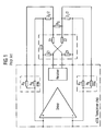
Figure 1 shows a xDSL transceiver for transmitting and receiving a xDSL signal according to the state of the art. The xDSL transceiver comprises a line driver for driving a transmission signal applied to a signal input of the analog line driver via a signal line which is formed e.g. by a pair of copper wires. The output of the line driver is connected via a transformer (not shown) to the transmission line. The transmission line comprises a complex line impedance ZL. - The xDSL transceiver according to the state of the art as shown in
figure 1 further comprises a receiver for evaluating a reception signal received via the signal line and applied to a signal input of that receiver. As shown infigure 1 a sense resistor RS is connected to the output terminal of the xDSL transceiver for sensing the output current of the line driver. - A feedback resistor network (FRN) is provided between the output terminal of the xDSL transceiver and the signal input of the analog line driver. The feedback resistor network FRN is provided for forming a synthesized termination output impedance ZT of the xDSL transceiver as a product of the sense resistor RS and a synthesis factor. The feedback resistor network FRN of the xDSL transceiver according to the state of the art is formed by at least two resistors RA, RB. The resistors of the feedback resistor networks are set so that the termination impedance ZT of the xDSL transceiver matches the load impedance ZL of the transmission line. The xDSL transceiver according to the state of the art comprises an active termination impedance formed by the sense resistor RS and the feedback resistor network FRN. The feedback resistor network FRN is normally integrated with the line driver and the receiver on a xDSL transceiver chip.
- The xDSL transceiver according to the state of the art as shown in
figure 1 comprises an echo canceling bridge (ECB) which is provided for minimizing the transmission signal generated by the line driver at the signal input of the receiver. The echo canceling bridge ECB is formed fully differential and comprises two pairs of complex impedances Z1, Z2. Since the impedances Z1, Z2 of the echo canceling bridge ECB are not purely resistive but complex it is difficult to integrate these components on the xDSL transceiver chip. Accordingly the echo canceling bridge ECB of the xDSL transceiver according to the state of the art as shown infigure 1 is not integrated in the xDSL transceiver chip. - Consequently a first disadvantage of the xDSL transceiver according to the state of the art as shown in
figure 1 is that the echo canceling bridge ECR is not integrated on the transceiver chip thus increasing the size of the xDSL transceiver line card and the production costs. Further it is more likely that the echo canceling bridge ECB which is provided outside the xDSL transceiver chip picks up noise from the surrounding e.g. the noise sensitivity of the receiver is increased. - An even more severe drawback of the conventional xDSL transceiver as shown in
figure 1 is that because of the resistive sense resistor RS the matching between the synthesized termination impedance ZT of the xDSL transceiver and the load impedance ZL of the transmission line is far from perfect so that the transmission gain is not a flat curve over the broadband frequency range i.e. the transmission gain is not constant. - Accordingly it is the main object of the invention to provide a xDSL transceiver having a synthesized termination output impedance ZT which matches the load impedance ZL of the transmission line over a broad frequency range.
- This object is achieved by a broadband xDSL transceiver having the features of main claim 1.
- The invention provides a broadband xDSL transceiver for transmitting and receiving signals in a broadband frequency range via a signal line which has a complex line impedance ZL,
wherein the xDSL transceiver comprises - a line driver for driving a transmission signal applied to a signal input of said line driver via said signal line,
- a receiver for evaluating a reception signal received via said signal line and applied to a signal input of said receiver,
- an echo canceling bridge for canceling the transmission signal at the signal input of said receiver,
- a sense impedance (ZS) connected to the signal line,
- a feedback resistor network provided between the sense impedance (ZS) and the signal input of said line driver for forming a synthesized termination impedance (ZT) of the xDSL transceiver as a product of the sense impedance (ZS) and an impedance synthesis factor (G),
- wherein the sense impedance (ZS) is a complex impedance so that the synthesized termination impedance (ZT) matches the line impedance (ZL) over all frequencies in the predetermined broadband frequency range.
- In a preferred embodiment the feedback resistor network is programmable to adjust the impedance synthesis factor (G).
- This has the advantage that the synthesized termination impedance (ZT) of the xDSL transceiver is adaptable to different transmission lines having different load impedances (ZL).
- In a further preferred embodiment of the xDSL transceiver according to the present invention the echo canceling bridge is programmable to minimize the transmission signal at the signal input of the receiver.
- In a preferred embodiment the line driver, the receiver, the feedback resistor network and the echo canceling bridge are integrated on a xDSL transceiver chip.
- The integration of the echo canceling bridge on the xDSL transceiver chip has the advantage that the size of the xDSL transceiver line card is decreased.
- A further advantage is that the production costs for a broadband xDSL transceiver are decreased.
- A further advantage of integrating the echo canceling bridge within the xDSL transceiver chip is that the noise sensitivity of the receiver is diminished, i.e. it is less likely that the receiver picks up crosstalk from the surrounding.
- In a preferred embodiment the xDSL transceiver is formed fully differential.
- In a further embodiment the line driver comprises a signal output which is connected via a transformer to the signal line.
- In a preferred embodiment the echo canceling bridge is formed by a resistor network comprising resistors which are integrated on the xDSL transceiver chip.
- In the following preferred embodiments of the programmable xDSL transceiver according to the present invention are described with reference to the enclosed figures.
- Figure 1
- shows an xDSL transceiver according to the state of the art;
- Figure 2
- shows a first embodiment of the broadband xDSL transceiver according to the present invention;
- Figure 3
- shows a second embodiment of the broadband xDSL transceiver according to the present invention.
- As can be seen from
figure 2 the broadband xDSL transceiver 1according to the present invention comprises axDSL transceiver chip 2 including a line driver 3 for driving a transmission signal applied to asignal input internal signal lines output terminals xDSL transceiver chip 2. Theoutput terminal xDSL transceiver chip 2 are connected via a transformer not shown to the transmission line having a load impedance ZL. The impedance ZL of the transmission line is complex. The transmission line is shown asimpedances figure 2 . - The xDSL transceiver 1 further comprises a
receiver 8 for evaluating a reception signal received via the signal line and applied to asignal input receiver 8. The xDSL transceiver 1 further comprises anecho canceling bridge 10 for canceling the transmission signal at thesignal input receiver 8. Asense impedance 11 is connected to the signal line. Thesense impedance 11 of the xDSL transceiver 1 according to the present invention is like the impedance ZL of the transmission line also complex. Thesense impedance 11 having the complex impedance ZS is in the embodiment shown infigure 2 not integrated in thexDSL transceiver chip 2. - The
signal terminals xDSL transceiver chip 2 are fedback viafirst feedback lines 12a, 12b toterminals xDSL transceiver chip 2. Theterminals internal lines feedback resistor networks sense impedance 11 of the xDSL transceiver 1 is connected via secondexternal feedback lines terminals xDSL transceiver chip 2.Theses terminals internal lines feedback resistor networks feedback resistor networks feedback resistor networks feedback resistor networks internal feedback lines line driver input - The
echo canceling bridge 10 comprises two pairs of resistors R1, R2. The resistors R1, R2 do not have a complex impedance and are purely resistive so that they can be integrated easily on thexDSL transceiver chip 2. A first resistor R1 is provided between theinternal signal lines signal input receiver 8. The second resistor R2 is connected between thecomplex sense impedance 11 and thesignal input receiver 8. - In a preferred embodiment the
echo canceling bridge 10 is also programmable by means of internalprogramming control lines signal input receiver 8 is minimized. The programmableecho canceling bridge 10 comprises switches (not shown) which are controlled by means of thecontrol lines programming control lines - The
feedback resistor networks sense impedance 11 and thesignal input - The termination impedance ZT of the xDSL transceiver 1 is the product of the sense impedance ZS and an adjustable impedance synthesis factor (G):

- Optimal matching is achieved when the termination impedance ZT is identical to the load impedance ZL of the signal line:

- Consequently:

- The transmission gain of the transmit signal generated by the line driver 3 at the
receiver input 
- When the load impedance ZL is known it can be achieved that the transmission gain GTX becomes zero by correctly dimensioning the resistances R1, R2 of the resistors within the
echo canceling bridge 10 and the complex impedance ZS ofimpedance 11. - Accordingly the
echo canceling bridge 10 can be implemented in such a manner that the transmission signal is cancelled almost completely at the signal input of thereceiver 8 thereby achieving a minimized crosstalk. - The gain of the reception signal GRX given by:

- The resistors R1, R2 of the echo canceling bridge are dimensioned in such a way that the gain G is minimized. The synthesis factor G is chosen to be sufficiently high to have an acceptable reception signal gain GRX but still low enough to achieve a low power dissipation.
- When decreasing the impedance ZS thus minimizing power dissipation this has as a trade off that the gain of the reception signal GRX is decreased.
- As can be seen from equation (4) since the sense resistor has also a complex impedance ZS like the impedance of the signal line the quotient

- Since the
impedance 11 is complex (ZS) it is possible in the xDSL transceiver 1 to use anecho canceling bridge 10 which is pure resistive i.e. which comprises only resistors which do not have a complex impedance. Consequently theecho canceling bridge 10 of the xDSL transceiver 1 according to the present invention can be easily integrated of thexDSL transceiver chip 2. Accordingly the xDSL transceiver 1 achieves a superior matching and minimized crosstalk at the same time. Further the xDSL transceiver 1 according to the present invention is smaller in size and can be produced with lower costs. -
Figure 3 shows an alternative embodiment of the xDSL transceiver 1 according to the present invention. - In this embodiment the sense impedance ZS is connected in series to the load impedance ZL, i.e. with or without using of a transformer. The second resistor R1 of the
echo canceling bridge 10 is provided between thesignal input receiver 8 andterminals - In typical applications the load impedance ZL of the signal line is about 100 ohm. To minimize the impedance of the
sensing resistor 11 and to minimize the power dissipation feedback loops are employed to form a synthesized termination impedance ZT which matches the load impedance ZL of the signal line, i.e. the termination impedance is typically also around 100 ohm. In a typical embodiment of the xDSL transceiver 1 according to the present invention the impedance synthesis factor G is about 7.
Claims (7)
- Broadband xDSL transceiver for transmitting and receiving signals in a predetermined broadband frequency range (F) via a signal line which has a complex line impedance (ZL), wherein the xDSL transceiver (1) comprises:(a) a line driver (3) for driving a transmission signal applied to a signal input (4a, 4b) of said line driver (3) via said signal line;(b) a receiver (8) for evaluating a reception signal received via said signal line and applied to a signal input of said receiver (8);(c) an echo canceling bridge (10) for canceling the transmission signal at the signal input (9a, 9b) of said receiver (8) ;(d) a sense impedance (11) connected to the signal line;(e) a feedback resistor network (15a, 15b) provided between the sense impedance (11) and the signal input (4a, 4b) of said line driver (3) for forming a synthesized termination impedance (ZT) of the xDSL transceiver (1) as a product of the sense impedance and an impedance synthesis factor (G);(f) wherein the sense impedance (11) is a complex impedance (ZS) so that the synthesized termination impedance (ZT) matches the line impedance (ZL) over the predetermined broadband frequency range F), characterized in that the echo canceling bridge includes at least one switchably connectable resistor.
- The broadband xDSL transceiver according to claim 1 wherein the feedback resistor network (15a, 15b) is programmable to adjust the impedance synthesis factor (G).
- The broadband xDSL transceiver according to claim 1 wherein the echo canceling bridge (10) is programmable to minimize the transmission signal at the signal input (9a, 9b) of the receiver (8).
- The broadband xDSL transceiver according to claim 1 wherein the line driver (3), the receiver (8), the feedback resistor network (15a, 15b) and the echo canceling bridge (10) are integrated on a xDSL transceiver chip (2).
- The broadband xDSL transceiver according to claim 1 wherein the xDSL transceiver (1) is formed fully differential.
- The broadband xDSL transceiver according to claim 1 wherein the line driver (3) comprises a signal output which is connected via a transformer to the signal line.
- The broadband xDSL transceiver according to claim 6 wherein the echo canceling bridge (10) is formed by a resistor network comprising resistors (R1, R2) which are integrated on said xDSL transceiver chip (2).
Priority Applications (3)
| Application Number | Priority Date | Filing Date | Title |
|---|---|---|---|
| EP04015203A EP1612962B1 (en) | 2004-06-29 | 2004-06-29 | Broadband xDSL transceiver |
| CNA2005100754141A CN1716799A (en) | 2004-06-29 | 2005-06-01 | Broadband XDSL transceiver |
| US11/170,395 US20050286710A1 (en) | 2004-06-29 | 2005-06-29 | Broadband XDSL transceiver |
Applications Claiming Priority (1)
| Application Number | Priority Date | Filing Date | Title |
|---|---|---|---|
| EP04015203A EP1612962B1 (en) | 2004-06-29 | 2004-06-29 | Broadband xDSL transceiver |
Publications (2)
| Publication Number | Publication Date |
|---|---|
| EP1612962A1 EP1612962A1 (en) | 2006-01-04 |
| EP1612962B1 true EP1612962B1 (en) | 2011-09-28 |
Family
ID=34925533
Family Applications (1)
| Application Number | Title | Priority Date | Filing Date |
|---|---|---|---|
| EP04015203A Expired - Lifetime EP1612962B1 (en) | 2004-06-29 | 2004-06-29 | Broadband xDSL transceiver |
Country Status (3)
| Country | Link |
|---|---|
| US (1) | US20050286710A1 (en) |
| EP (1) | EP1612962B1 (en) |
| CN (1) | CN1716799A (en) |
Families Citing this family (3)
| Publication number | Priority date | Publication date | Assignee | Title |
|---|---|---|---|---|
| SE520184C2 (en) * | 2001-10-11 | 2003-06-10 | Ericsson Telefon Ab L M | Ekosläckningsanordning |
| CN101359932B (en) * | 2008-09-03 | 2012-08-29 | 华为技术有限公司 | DSL circuit driving device, method and access system |
| CN101807892B (en) * | 2009-02-13 | 2012-08-29 | 瑞昱半导体股份有限公司 | Line driver with function of automatically adjusting output impedance |
Family Cites Families (5)
| Publication number | Priority date | Publication date | Assignee | Title |
|---|---|---|---|---|
| CA2277534A1 (en) * | 1999-07-13 | 2001-01-13 | Jim Hjartarson | Combined xdsl and voice line card |
| EP1107464A1 (en) * | 1999-12-06 | 2001-06-13 | Alcatel | Method and device for echo cancelling |
| US6956944B1 (en) * | 1999-12-14 | 2005-10-18 | Orckit Communications, Ltd. | Method and apparatus for compensating for an echo signal component in telecommunication systems |
| SE520184C2 (en) * | 2001-10-11 | 2003-06-10 | Ericsson Telefon Ab L M | Ekosläckningsanordning |
| ATE314769T1 (en) * | 2002-01-04 | 2006-01-15 | Cit Alcatel | IMPENDANCE ADJUSTMENT FOR LINE DRIVER |
-
2004
- 2004-06-29 EP EP04015203A patent/EP1612962B1/en not_active Expired - Lifetime
-
2005
- 2005-06-01 CN CNA2005100754141A patent/CN1716799A/en active Pending
- 2005-06-29 US US11/170,395 patent/US20050286710A1/en not_active Abandoned
Also Published As
| Publication number | Publication date |
|---|---|
| EP1612962A1 (en) | 2006-01-04 |
| US20050286710A1 (en) | 2005-12-29 |
| CN1716799A (en) | 2006-01-04 |
Similar Documents
| Publication | Publication Date | Title |
|---|---|---|
| CN1848699B (en) | Multi-path active hybrid circuit and corresponding method | |
| US5119365A (en) | Bi-directional buffer line amplifier | |
| US7282992B2 (en) | Class D-amplifier | |
| US20020119753A1 (en) | Programmable echo cancellation filter | |
| US7483528B2 (en) | Loop extender with selectable line termination and equalization | |
| US7406117B2 (en) | XDSL multi-hybrid modem with power spectral density shaping | |
| US7881458B2 (en) | Method and apparatus for adaptive hybrid termination in a multi-carrier communication system | |
| US20030201759A1 (en) | Full duplexing for power line data communications | |
| EP1391055B1 (en) | Line interface with a matching impedance coupled to a feedback path | |
| US20050286710A1 (en) | Broadband XDSL transceiver | |
| US5541990A (en) | Compensated hybrid | |
| KR100427231B1 (en) | Analog echo filter | |
| JP2001211105A (en) | Method and device for echo cancelation | |
| US8570074B2 (en) | Method and apparatus for reducing transmitter AC-coupling droop | |
| CN112929055B (en) | Echo cancellation circuit | |
| CN100386967C (en) | Transceiver with integrated hybrid circuit | |
| KR100631383B1 (en) | Bridge circuit to suppress echoes in communication devices | |
| CN1655468B (en) | Adjustable echo eliminating apparatus for all duplex communication systems | |
| EP1560408B1 (en) | xDSL-line-interface-circuit | |
| US7031378B1 (en) | Unified DSL transceiver | |
| De Wilde et al. | Analog front end for DMT-based VDSL | |
| EP1089450B1 (en) | Telephone line interface circuit | |
| US20020075962A1 (en) | Digital transmission line tap circuit | |
| US20020186824A1 (en) | Splitterless, transformerless, voice service independent ADSL interface | |
| US6930567B2 (en) | Transmission system |
Legal Events
| Date | Code | Title | Description |
|---|---|---|---|
| PUAI | Public reference made under article 153(3) epc to a published international application that has entered the european phase |
Free format text: ORIGINAL CODE: 0009012 |
|
| AK | Designated contracting states |
Kind code of ref document: A1 Designated state(s): AT BE BG CH CY CZ DE DK EE ES FI FR GB GR HU IE IT LI LU MC NL PL PT RO SE SI SK TR |
|
| AX | Request for extension of the european patent |
Extension state: AL HR LT LV MK |
|
| 17P | Request for examination filed |
Effective date: 20060117 |
|
| AKX | Designation fees paid |
Designated state(s): AT BE BG CH LI |
|
| RBV | Designated contracting states (corrected) |
Designated state(s): DE FR GB IT |
|
| REG | Reference to a national code |
Ref country code: DE Ref legal event code: 8566 |
|
| 17Q | First examination report despatched |
Effective date: 20100212 |
|
| RAP1 | Party data changed (applicant data changed or rights of an application transferred) |
Owner name: INFINEON TECHNOLOGIES AG |
|
| RAP1 | Party data changed (applicant data changed or rights of an application transferred) |
Owner name: LANTIQ DEUTSCHLAND GMBH |
|
| GRAP | Despatch of communication of intention to grant a patent |
Free format text: ORIGINAL CODE: EPIDOSNIGR1 |
|
| GRAS | Grant fee paid |
Free format text: ORIGINAL CODE: EPIDOSNIGR3 |
|
| GRAA | (expected) grant |
Free format text: ORIGINAL CODE: 0009210 |
|
| AK | Designated contracting states |
Kind code of ref document: B1 Designated state(s): DE FR GB IT |
|
| REG | Reference to a national code |
Ref country code: GB Ref legal event code: FG4D |
|
| REG | Reference to a national code |
Ref country code: DE Ref legal event code: R096 Ref document number: 602004034507 Country of ref document: DE Effective date: 20111201 |
|
| PG25 | Lapsed in a contracting state [announced via postgrant information from national office to epo] |
Ref country code: IT Free format text: LAPSE BECAUSE OF FAILURE TO SUBMIT A TRANSLATION OF THE DESCRIPTION OR TO PAY THE FEE WITHIN THE PRESCRIBED TIME-LIMIT Effective date: 20110928 |
|
| PLBE | No opposition filed within time limit |
Free format text: ORIGINAL CODE: 0009261 |
|
| STAA | Information on the status of an ep patent application or granted ep patent |
Free format text: STATUS: NO OPPOSITION FILED WITHIN TIME LIMIT |
|
| 26N | No opposition filed |
Effective date: 20120629 |
|
| REG | Reference to a national code |
Ref country code: DE Ref legal event code: R097 Ref document number: 602004034507 Country of ref document: DE Effective date: 20120629 |
|
| REG | Reference to a national code |
Ref country code: FR Ref legal event code: PLFP Year of fee payment: 13 |
|
| REG | Reference to a national code |
Ref country code: FR Ref legal event code: PLFP Year of fee payment: 14 |
|
| REG | Reference to a national code |
Ref country code: GB Ref legal event code: 732E Free format text: REGISTERED BETWEEN 20180208 AND 20180214 |
|
| REG | Reference to a national code |
Ref country code: DE Ref legal event code: R081 Ref document number: 602004034507 Country of ref document: DE Owner name: INTEL CORP., SANTA CLARA, US Free format text: FORMER OWNER: LANTIQ DEUTSCHLAND GMBH, 85579 NEUBIBERG, DE Ref country code: DE Ref legal event code: R081 Ref document number: 602004034507 Country of ref document: DE Owner name: LANTIQ BETEILIGUNGS-GMBH & CO. KG, DE Free format text: FORMER OWNER: LANTIQ DEUTSCHLAND GMBH, 85579 NEUBIBERG, DE |
|
| REG | Reference to a national code |
Ref country code: FR Ref legal event code: PLFP Year of fee payment: 15 |
|
| PGFP | Annual fee paid to national office [announced via postgrant information from national office to epo] |
Ref country code: FR Payment date: 20180529 Year of fee payment: 15 |
|
| REG | Reference to a national code |
Ref country code: FR Ref legal event code: CA Effective date: 20180807 |
|
| REG | Reference to a national code |
Ref country code: FR Ref legal event code: TP Owner name: LANTIQ BETEILIGUNGS-GMBH & CO. KG, DE Effective date: 20180903 |
|
| PG25 | Lapsed in a contracting state [announced via postgrant information from national office to epo] |
Ref country code: FR Free format text: LAPSE BECAUSE OF NON-PAYMENT OF DUE FEES Effective date: 20190630 |
|
| PGFP | Annual fee paid to national office [announced via postgrant information from national office to epo] |
Ref country code: DE Payment date: 20200617 Year of fee payment: 17 |
|
| PGFP | Annual fee paid to national office [announced via postgrant information from national office to epo] |
Ref country code: GB Payment date: 20200618 Year of fee payment: 17 |
|
| REG | Reference to a national code |
Ref country code: DE Ref legal event code: R081 Ref document number: 602004034507 Country of ref document: DE Owner name: INTEL CORP., SANTA CLARA, US Free format text: FORMER OWNER: LANTIQ BETEILIGUNGS-GMBH & CO. KG, 85579 NEUBIBERG, DE |
|
| REG | Reference to a national code |
Ref country code: GB Ref legal event code: 732E Free format text: REGISTERED BETWEEN 20200827 AND 20200902 |
|
| REG | Reference to a national code |
Ref country code: DE Ref legal event code: R119 Ref document number: 602004034507 Country of ref document: DE |
|
| GBPC | Gb: european patent ceased through non-payment of renewal fee |
Effective date: 20210629 |
|
| PG25 | Lapsed in a contracting state [announced via postgrant information from national office to epo] |
Ref country code: GB Free format text: LAPSE BECAUSE OF NON-PAYMENT OF DUE FEES Effective date: 20210629 Ref country code: DE Free format text: LAPSE BECAUSE OF NON-PAYMENT OF DUE FEES Effective date: 20220101 |