EP1612866A2 - ALGaN/GaN Hemt Devices - Google Patents
ALGaN/GaN Hemt Devices Download PDFInfo
- Publication number
- EP1612866A2 EP1612866A2 EP05447155A EP05447155A EP1612866A2 EP 1612866 A2 EP1612866 A2 EP 1612866A2 EP 05447155 A EP05447155 A EP 05447155A EP 05447155 A EP05447155 A EP 05447155A EP 1612866 A2 EP1612866 A2 EP 1612866A2
- Authority
- EP
- European Patent Office
- Prior art keywords
- layer
- active layer
- semiconductor device
- fabricating
- passivation layer
- Prior art date
- Legal status (The legal status is an assumption and is not a legal conclusion. Google has not performed a legal analysis and makes no representation as to the accuracy of the status listed.)
- Granted
Links
- 238000000034 method Methods 0.000 claims abstract description 78
- 229910002704 AlGaN Inorganic materials 0.000 claims abstract description 76
- 238000000151 deposition Methods 0.000 claims abstract description 34
- 238000001816 cooling Methods 0.000 claims abstract description 16
- 238000002488 metal-organic chemical vapour deposition Methods 0.000 claims abstract description 7
- 238000002161 passivation Methods 0.000 claims description 130
- 239000004065 semiconductor Substances 0.000 claims description 70
- 239000000758 substrate Substances 0.000 claims description 48
- 239000000463 material Substances 0.000 claims description 44
- 150000004767 nitrides Chemical class 0.000 claims description 26
- 238000006243 chemical reaction Methods 0.000 claims description 24
- 230000005533 two-dimensional electron gas Effects 0.000 claims description 22
- IJGRMHOSHXDMSA-UHFFFAOYSA-N Atomic nitrogen Chemical compound N#N IJGRMHOSHXDMSA-UHFFFAOYSA-N 0.000 claims description 20
- 125000006850 spacer group Chemical group 0.000 claims description 14
- 229910052757 nitrogen Inorganic materials 0.000 claims description 11
- 229910052594 sapphire Inorganic materials 0.000 claims description 11
- 239000010980 sapphire Substances 0.000 claims description 11
- 229910002601 GaN Inorganic materials 0.000 claims description 10
- 229910017083 AlN Inorganic materials 0.000 claims description 9
- 229910052710 silicon Inorganic materials 0.000 claims description 9
- 239000010703 silicon Substances 0.000 claims description 7
- 239000013078 crystal Substances 0.000 claims description 6
- 229910003465 moissanite Inorganic materials 0.000 claims description 6
- 229910010271 silicon carbide Inorganic materials 0.000 claims description 6
- 238000005530 etching Methods 0.000 claims description 5
- 230000007704 transition Effects 0.000 claims description 5
- 230000005669 field effect Effects 0.000 abstract description 12
- 238000004519 manufacturing process Methods 0.000 abstract 1
- 239000012808 vapor phase Substances 0.000 abstract 1
- 230000015572 biosynthetic process Effects 0.000 description 26
- QGZKDVFQNNGYKY-UHFFFAOYSA-N Ammonia Chemical compound N QGZKDVFQNNGYKY-UHFFFAOYSA-N 0.000 description 18
- BLRPTPMANUNPDV-UHFFFAOYSA-N Silane Chemical compound [SiH4] BLRPTPMANUNPDV-UHFFFAOYSA-N 0.000 description 15
- 238000011065 in-situ storage Methods 0.000 description 12
- 230000008021 deposition Effects 0.000 description 11
- 238000005259 measurement Methods 0.000 description 11
- 229910000069 nitrogen hydride Inorganic materials 0.000 description 10
- 229910052751 metal Inorganic materials 0.000 description 9
- 239000002184 metal Substances 0.000 description 9
- 238000012545 processing Methods 0.000 description 9
- 230000000694 effects Effects 0.000 description 8
- 229910000077 silane Inorganic materials 0.000 description 8
- XCZXGTMEAKBVPV-UHFFFAOYSA-N trimethylgallium Chemical compound C[Ga](C)C XCZXGTMEAKBVPV-UHFFFAOYSA-N 0.000 description 8
- 239000000956 alloy Substances 0.000 description 7
- 229910045601 alloy Inorganic materials 0.000 description 7
- 230000006872 improvement Effects 0.000 description 7
- 229910052719 titanium Inorganic materials 0.000 description 7
- 235000012431 wafers Nutrition 0.000 description 6
- 229910052581 Si3N4 Inorganic materials 0.000 description 5
- XUIMIQQOPSSXEZ-UHFFFAOYSA-N Silicon Chemical compound [Si] XUIMIQQOPSSXEZ-UHFFFAOYSA-N 0.000 description 5
- 230000001419 dependent effect Effects 0.000 description 5
- 229910052737 gold Inorganic materials 0.000 description 5
- 229910052750 molybdenum Inorganic materials 0.000 description 5
- 229910052759 nickel Inorganic materials 0.000 description 5
- 230000006911 nucleation Effects 0.000 description 5
- 238000010899 nucleation Methods 0.000 description 5
- 229910052763 palladium Inorganic materials 0.000 description 5
- 230000001603 reducing effect Effects 0.000 description 5
- 230000009467 reduction Effects 0.000 description 5
- JLTRXTDYQLMHGR-UHFFFAOYSA-N trimethylaluminium Chemical compound C[Al](C)C JLTRXTDYQLMHGR-UHFFFAOYSA-N 0.000 description 5
- VYPSYNLAJGMNEJ-UHFFFAOYSA-N Silicium dioxide Chemical compound O=[Si]=O VYPSYNLAJGMNEJ-UHFFFAOYSA-N 0.000 description 4
- 229910052782 aluminium Inorganic materials 0.000 description 4
- 229910021529 ammonia Inorganic materials 0.000 description 4
- 230000009286 beneficial effect Effects 0.000 description 4
- 238000011066 ex-situ storage Methods 0.000 description 4
- 238000001020 plasma etching Methods 0.000 description 4
- 230000001105 regulatory effect Effects 0.000 description 4
- UFHFLCQGNIYNRP-UHFFFAOYSA-N Hydrogen Chemical compound [H][H] UFHFLCQGNIYNRP-UHFFFAOYSA-N 0.000 description 3
- 238000000137 annealing Methods 0.000 description 3
- 239000013590 bulk material Substances 0.000 description 3
- 229910052799 carbon Inorganic materials 0.000 description 3
- 238000011109 contamination Methods 0.000 description 3
- 239000001257 hydrogen Substances 0.000 description 3
- 229910052739 hydrogen Inorganic materials 0.000 description 3
- 150000002739 metals Chemical class 0.000 description 3
- 238000001451 molecular beam epitaxy Methods 0.000 description 3
- 229910052758 niobium Inorganic materials 0.000 description 3
- 230000003647 oxidation Effects 0.000 description 3
- 238000007254 oxidation reaction Methods 0.000 description 3
- 230000008569 process Effects 0.000 description 3
- HQVNEWCFYHHQES-UHFFFAOYSA-N silicon nitride Chemical compound N12[Si]34N5[Si]62N3[Si]51N64 HQVNEWCFYHHQES-UHFFFAOYSA-N 0.000 description 3
- 239000007858 starting material Substances 0.000 description 3
- 238000012546 transfer Methods 0.000 description 3
- 229910052720 vanadium Inorganic materials 0.000 description 3
- 229910052726 zirconium Inorganic materials 0.000 description 3
- 229910020776 SixNy Inorganic materials 0.000 description 2
- 238000005229 chemical vapour deposition Methods 0.000 description 2
- 229910052804 chromium Inorganic materials 0.000 description 2
- 229910052681 coesite Inorganic materials 0.000 description 2
- 150000001875 compounds Chemical class 0.000 description 2
- 238000005336 cracking Methods 0.000 description 2
- 229910052906 cristobalite Inorganic materials 0.000 description 2
- 239000002019 doping agent Substances 0.000 description 2
- 238000005516 engineering process Methods 0.000 description 2
- 238000002955 isolation Methods 0.000 description 2
- 238000001465 metallisation Methods 0.000 description 2
- 239000000203 mixture Substances 0.000 description 2
- 238000000623 plasma-assisted chemical vapour deposition Methods 0.000 description 2
- 229910052697 platinum Inorganic materials 0.000 description 2
- 238000002360 preparation method Methods 0.000 description 2
- 238000000926 separation method Methods 0.000 description 2
- 239000000377 silicon dioxide Substances 0.000 description 2
- 229910052682 stishovite Inorganic materials 0.000 description 2
- 229910052905 tridymite Inorganic materials 0.000 description 2
- 238000000927 vapour-phase epitaxy Methods 0.000 description 2
- -1 Magnesium nitride Chemical class 0.000 description 1
- 230000001154 acute effect Effects 0.000 description 1
- QVGXLLKOCUKJST-UHFFFAOYSA-N atomic oxygen Chemical compound [O] QVGXLLKOCUKJST-UHFFFAOYSA-N 0.000 description 1
- 230000008901 benefit Effects 0.000 description 1
- 239000012159 carrier gas Substances 0.000 description 1
- 230000015556 catabolic process Effects 0.000 description 1
- 230000008859 change Effects 0.000 description 1
- 238000004140 cleaning Methods 0.000 description 1
- 238000010924 continuous production Methods 0.000 description 1
- 230000003247 decreasing effect Effects 0.000 description 1
- 230000007547 defect Effects 0.000 description 1
- 238000007872 degassing Methods 0.000 description 1
- 238000003795 desorption Methods 0.000 description 1
- 238000011161 development Methods 0.000 description 1
- 239000006185 dispersion Substances 0.000 description 1
- 238000000609 electron-beam lithography Methods 0.000 description 1
- 238000011049 filling Methods 0.000 description 1
- 229910052733 gallium Inorganic materials 0.000 description 1
- 239000007789 gas Substances 0.000 description 1
- 238000002017 high-resolution X-ray diffraction Methods 0.000 description 1
- 238000002513 implantation Methods 0.000 description 1
- 238000001459 lithography Methods 0.000 description 1
- 229910052749 magnesium Inorganic materials 0.000 description 1
- 239000011777 magnesium Substances 0.000 description 1
- 229910044991 metal oxide Inorganic materials 0.000 description 1
- 150000004706 metal oxides Chemical class 0.000 description 1
- 230000004048 modification Effects 0.000 description 1
- 238000012986 modification Methods 0.000 description 1
- 230000007935 neutral effect Effects 0.000 description 1
- 230000003287 optical effect Effects 0.000 description 1
- 229910052760 oxygen Inorganic materials 0.000 description 1
- 239000001301 oxygen Substances 0.000 description 1
- 230000035515 penetration Effects 0.000 description 1
- 230000010287 polarization Effects 0.000 description 1
- 239000002243 precursor Substances 0.000 description 1
- 238000004151 rapid thermal annealing Methods 0.000 description 1
- 239000013074 reference sample Substances 0.000 description 1
- 229910052711 selenium Inorganic materials 0.000 description 1
- 230000002269 spontaneous effect Effects 0.000 description 1
- 239000000126 substance Substances 0.000 description 1
- 230000008719 thickening Effects 0.000 description 1
- YFNCATAIYKQPOO-UHFFFAOYSA-N thiophanate Chemical compound CCOC(=O)NC(=S)NC1=CC=CC=C1NC(=S)NC(=O)OCC YFNCATAIYKQPOO-UHFFFAOYSA-N 0.000 description 1
- XLYOFNOQVPJJNP-UHFFFAOYSA-N water Substances O XLYOFNOQVPJJNP-UHFFFAOYSA-N 0.000 description 1
- 229910052984 zinc sulfide Inorganic materials 0.000 description 1
Images


Classifications
-
- H—ELECTRICITY
- H01—ELECTRIC ELEMENTS
- H01L—SEMICONDUCTOR DEVICES NOT COVERED BY CLASS H10
- H01L23/00—Details of semiconductor or other solid state devices
- H01L23/28—Encapsulations, e.g. encapsulating layers, coatings, e.g. for protection
- H01L23/31—Encapsulations, e.g. encapsulating layers, coatings, e.g. for protection characterised by the arrangement or shape
- H01L23/3157—Partial encapsulation or coating
- H01L23/3171—Partial encapsulation or coating the coating being directly applied to the semiconductor body, e.g. passivation layer
-
- H—ELECTRICITY
- H01—ELECTRIC ELEMENTS
- H01L—SEMICONDUCTOR DEVICES NOT COVERED BY CLASS H10
- H01L29/00—Semiconductor devices adapted for rectifying, amplifying, oscillating or switching, or capacitors or resistors with at least one potential-jump barrier or surface barrier, e.g. PN junction depletion layer or carrier concentration layer; Details of semiconductor bodies or of electrodes thereof ; Multistep manufacturing processes therefor
- H01L29/02—Semiconductor bodies ; Multistep manufacturing processes therefor
- H01L29/06—Semiconductor bodies ; Multistep manufacturing processes therefor characterised by their shape; characterised by the shapes, relative sizes, or dispositions of the semiconductor regions ; characterised by the concentration or distribution of impurities within semiconductor regions
- H01L29/08—Semiconductor bodies ; Multistep manufacturing processes therefor characterised by their shape; characterised by the shapes, relative sizes, or dispositions of the semiconductor regions ; characterised by the concentration or distribution of impurities within semiconductor regions with semiconductor regions connected to an electrode carrying current to be rectified, amplified or switched and such electrode being part of a semiconductor device which comprises three or more electrodes
- H01L29/0895—Tunnel injectors
-
- H—ELECTRICITY
- H01—ELECTRIC ELEMENTS
- H01L—SEMICONDUCTOR DEVICES NOT COVERED BY CLASS H10
- H01L29/00—Semiconductor devices adapted for rectifying, amplifying, oscillating or switching, or capacitors or resistors with at least one potential-jump barrier or surface barrier, e.g. PN junction depletion layer or carrier concentration layer; Details of semiconductor bodies or of electrodes thereof ; Multistep manufacturing processes therefor
- H01L29/66—Types of semiconductor device ; Multistep manufacturing processes therefor
- H01L29/66007—Multistep manufacturing processes
- H01L29/66075—Multistep manufacturing processes of devices having semiconductor bodies comprising group 14 or group 13/15 materials
- H01L29/66227—Multistep manufacturing processes of devices having semiconductor bodies comprising group 14 or group 13/15 materials the devices being controllable only by the electric current supplied or the electric potential applied, to an electrode which does not carry the current to be rectified, amplified or switched, e.g. three-terminal devices
- H01L29/66409—Unipolar field-effect transistors
- H01L29/66446—Unipolar field-effect transistors with an active layer made of a group 13/15 material, e.g. group 13/15 velocity modulation transistor [VMT], group 13/15 negative resistance FET [NERFET]
- H01L29/66462—Unipolar field-effect transistors with an active layer made of a group 13/15 material, e.g. group 13/15 velocity modulation transistor [VMT], group 13/15 negative resistance FET [NERFET] with a heterojunction interface channel or gate, e.g. HFET, HIGFET, SISFET, HJFET, HEMT
-
- H—ELECTRICITY
- H01—ELECTRIC ELEMENTS
- H01L—SEMICONDUCTOR DEVICES NOT COVERED BY CLASS H10
- H01L29/00—Semiconductor devices adapted for rectifying, amplifying, oscillating or switching, or capacitors or resistors with at least one potential-jump barrier or surface barrier, e.g. PN junction depletion layer or carrier concentration layer; Details of semiconductor bodies or of electrodes thereof ; Multistep manufacturing processes therefor
- H01L29/66—Types of semiconductor device ; Multistep manufacturing processes therefor
- H01L29/68—Types of semiconductor device ; Multistep manufacturing processes therefor controllable by only the electric current supplied, or only the electric potential applied, to an electrode which does not carry the current to be rectified, amplified or switched
- H01L29/76—Unipolar devices, e.g. field effect transistors
- H01L29/772—Field effect transistors
- H01L29/778—Field effect transistors with two-dimensional charge carrier gas channel, e.g. HEMT ; with two-dimensional charge-carrier layer formed at a heterojunction interface
- H01L29/7786—Field effect transistors with two-dimensional charge carrier gas channel, e.g. HEMT ; with two-dimensional charge-carrier layer formed at a heterojunction interface with direct single heterostructure, i.e. with wide bandgap layer formed on top of active layer, e.g. direct single heterostructure MIS-like HEMT
- H01L29/7787—Field effect transistors with two-dimensional charge carrier gas channel, e.g. HEMT ; with two-dimensional charge-carrier layer formed at a heterojunction interface with direct single heterostructure, i.e. with wide bandgap layer formed on top of active layer, e.g. direct single heterostructure MIS-like HEMT with wide bandgap charge-carrier supplying layer, e.g. direct single heterostructure MODFET
-
- H—ELECTRICITY
- H01—ELECTRIC ELEMENTS
- H01L—SEMICONDUCTOR DEVICES NOT COVERED BY CLASS H10
- H01L23/00—Details of semiconductor or other solid state devices
- H01L23/28—Encapsulations, e.g. encapsulating layers, coatings, e.g. for protection
- H01L23/29—Encapsulations, e.g. encapsulating layers, coatings, e.g. for protection characterised by the material, e.g. carbon
- H01L23/291—Oxides or nitrides or carbides, e.g. ceramics, glass
-
- H—ELECTRICITY
- H01—ELECTRIC ELEMENTS
- H01L—SEMICONDUCTOR DEVICES NOT COVERED BY CLASS H10
- H01L29/00—Semiconductor devices adapted for rectifying, amplifying, oscillating or switching, or capacitors or resistors with at least one potential-jump barrier or surface barrier, e.g. PN junction depletion layer or carrier concentration layer; Details of semiconductor bodies or of electrodes thereof ; Multistep manufacturing processes therefor
- H01L29/02—Semiconductor bodies ; Multistep manufacturing processes therefor
- H01L29/12—Semiconductor bodies ; Multistep manufacturing processes therefor characterised by the materials of which they are formed
- H01L29/20—Semiconductor bodies ; Multistep manufacturing processes therefor characterised by the materials of which they are formed including, apart from doping materials or other impurities, only AIIIBV compounds
- H01L29/2003—Nitride compounds
-
- H—ELECTRICITY
- H01—ELECTRIC ELEMENTS
- H01L—SEMICONDUCTOR DEVICES NOT COVERED BY CLASS H10
- H01L29/00—Semiconductor devices adapted for rectifying, amplifying, oscillating or switching, or capacitors or resistors with at least one potential-jump barrier or surface barrier, e.g. PN junction depletion layer or carrier concentration layer; Details of semiconductor bodies or of electrodes thereof ; Multistep manufacturing processes therefor
- H01L29/40—Electrodes ; Multistep manufacturing processes therefor
- H01L29/43—Electrodes ; Multistep manufacturing processes therefor characterised by the materials of which they are formed
- H01L29/49—Metal-insulator-semiconductor electrodes, e.g. gates of MOSFET
- H01L29/51—Insulating materials associated therewith
- H01L29/518—Insulating materials associated therewith the insulating material containing nitrogen, e.g. nitride, oxynitride, nitrogen-doped material
-
- H—ELECTRICITY
- H01—ELECTRIC ELEMENTS
- H01L—SEMICONDUCTOR DEVICES NOT COVERED BY CLASS H10
- H01L2924/00—Indexing scheme for arrangements or methods for connecting or disconnecting semiconductor or solid-state bodies as covered by H01L24/00
- H01L2924/0001—Technical content checked by a classifier
- H01L2924/0002—Not covered by any one of groups H01L24/00, H01L24/00 and H01L2224/00
-
- H—ELECTRICITY
- H01—ELECTRIC ELEMENTS
- H01L—SEMICONDUCTOR DEVICES NOT COVERED BY CLASS H10
- H01L2924/00—Indexing scheme for arrangements or methods for connecting or disconnecting semiconductor or solid-state bodies as covered by H01L24/00
- H01L2924/10—Details of semiconductor or other solid state devices to be connected
- H01L2924/11—Device type
- H01L2924/13—Discrete devices, e.g. 3 terminal devices
- H01L2924/1304—Transistor
- H01L2924/1306—Field-effect transistor [FET]
- H01L2924/13063—Metal-Semiconductor Field-Effect Transistor [MESFET]
Definitions
- the invention relates to the group III-nitride field effect devices, and methods to improve stability of the surface, by passivation of the top surface, as well as to ohmic contact deposition on wide bandgap layers.
- GaN Field-effect devices are piezoelectric devices, i.e. the presence of spontaneous and piezoelectric polarizations are responsible for charge separation within the material.
- 2DEG two-dimensional electron gas
- Presence of surface states creates acute problems for achieving the high performance that are theoretically predicted for those devices, as surface states play an important role during device operation. It has been noticed by many authors that the reduction of dc performance, current slump at high drain-source voltages, DC to RF dispersion phenomena, are directly related to the filling, emptying of surface states, although thermal effects are also partially responsible for dc current slump.
- US 2003/0020092 A1 describes an AlGaN/GaN HEMT having a thin AlGaN layer.
- Source and drain contacts contact the AlGaN layer, while parts of the AlGaN layer being uncovered by the contacts.
- An insulating layer covers the uncovered part of the AlGaN layer and a gate contact is included on the insulating layer.
- the HEMT and the insulating layer are fabricated using metal-organic chemical vapor deposition.
- the insulating layer is sputtered onto the top surface of the HEMT active layers.
- WO 01/13436 A1 describes a GaN based FET that employs dielectric passivation layers on exposed AlGaN or GaN surfaces of the devices above the channel regions, between the source and drain contacts.
- the dielectric layer is formed of SiN. The layer controls undesirable frequency-dependent current and reduced breakdown voltage.
- US 5,192,987 recites a high electron mobility transistor.
- the transistor consists of a GaN/AlGaN heterojunction, where a two-dimensional electron gas occurs.
- the structures are deposited on basal plane sapphire using low-pressure metal organic chemical vapor deposition.
- Another problem in the development of field-effect GaN based transistors is the ohmic contact formation on the group III-nitride surface.
- the ohmic contact formation is dependent on different factors, e.g. the surface composition, but one very important, which has long been underestimated, is the degree of oxidation of the top surface. Different cleaning techniques and metallization techniques have been suggested to overcome this problem.
- the lack of a good ohmic contact formation on the top layer directly leads to drastic reduction of the device performance. It is very often observed that the maximum current which is measured, under dc conditions, is well below the maximum current density values deduced from material considerations such as carrier density and mobility in the channel.
- a device comprising
- the passivation layer can be arranged such that the electron density in the two-dimensional electron-gas layer is increased.
- the gate contact is preferably in electrical contact with said second active layer.
- said first active layer is preferably formed of a group III nitride semiconductor material, more particularly of GaN.
- the second active layer is preferably formed of a group III nitride semiconductor material, more particularly of AlGaN or AlGaInN.
- a spacer layer can be positioned between the first active layer and the second active layer.
- a third layer preferably formed of a group III nitride material, can be positioned between said second active layer and said passivation layer.
- said passivation layer can be arranged such that it reduces or eliminates the effect of surface states on the carrier density in the two-dimensional electron gas, during device operation.
- said passivation layer is preferably formed of a material comprising at least an electron donating element and nitrogen, more particularly is formed of silicon nitride.
- the passivation layer can be a multi-layered structure comprising a group III nitride material and a material selected from the group consisting of SiN or AlN.
- the thickness of the passivation layer is preferably between 1 nm and 30 nm.
- the substrate is preferably formed of a material selected from the group consisting of silicon, sapphire, SiC, GaN and AlN.
- the source contact and the drain contact are deposited on the passivation layer.
- a device as recited in the previous embodiments is disclosed further comprising a gate contact in electrical contact with said second active layer.
- a part of said passivation layer is being uncovered by the source contact and the drain contacts.
- the gate contact can contact the passivation layer or the gate contact can be deposited on the second active layer.
- a device as recited in any of the previous embodiments wherein the first active layer is formed of a group III nitride semiconductor material.
- the first active layer is formed of GaN.
- said second active layer is formed of a group III nitride material.
- the second active layer is formed of AlGaN or AlGaInN.
- first active layer and the second active layer also called the interface
- surface charged layers could be created in the device.
- the surface charged layers are compensated by the formation of two-dimensional electron gas at the other side of the interface, resulting in high mobility values compared to the bulk material. This is beneficial for the creation of a very high mobility channel in the device.
- a spacer layer is present between the first active layer and the second active layer.
- the spacer layer is selected such that the mobility at the interface is increased.
- the spacer layer can be formed of, but is not limited hereto, AlN.
- the second active layer is partly or entirely doped with donor elements such as Si, to provide another source of electrons.
- the second active layer is covered by a third layer, the third layer being formed of a Group III nitride material such as, but not limited hereto, GaN.
- the third layer is between the second active layer and the passivation layer.
- the device can further comprise at least one buffer layer between the substrate and the first active layer.
- the buffer layer provides an appropriate crystal structure transition between the substrate and the remainder of the device.
- the buffer layer can be a nucleation layer between the substrate and the first active layer.
- the buffer layer can consist of, but is not limited hereto, AlN, GaN or AlGaN.
- the passivation is arranged such that it reduces or eliminates the effect of surface states on the carrier density in the two-dimensional electron gas, during device operation.
- a device as recited in any of the previous embodiments wherein said passivation layer comprises at least a donor material and nitrogen.
- the passivation layer is formed of silicon nitride.
- the passivation layer is formed of Magnesium nitride.
- the passivation layer is a multi-layered structure comprising a group III nitride material and a SiN or AlN.
- the passivation layer is arranged such that it reduces the effect of surface states on the carrier density in the two-dimensional electron gas, during device operation.
- the SiN layer could provide a charge neutral interface with the AlGaN, eliminating surface depletion of the 2DEG.
- the presence of high level of Si or at least donor-type of defects in the passivation layer could be are beneficial for the compensation of surface charge effects. Presence of surface states creates accurate problems for achieving the high performance, as surface states play an important role during device operation.
- the thickness of the passivation layer is between 1 nm and 100 nm, between 1 nm and 50 nm, between 1 nm and 30 nm, or between 1 nm and 20 nm. Preferably, the thickness is between 1 nm and 30 nm.
- the passivation layer is characterized by an amorphous structure.
- a thin passivation layer allows the formation of ohmic contacts with a low resistance.
- the passivation layer comprises Si, the Si can diffuse in the AlGaN, where it acts as a donor.
- the introduction of a donor type in the AlGaN layer facilitates the ohmic contact formation reducing thereby the contact resistance.
- the first active layer, the second active layer and the passivation layer are formed in the same reactor without subjecting the layers to air.
- the passivation layer is formed by MOVPE (Metal-Organic Vapor Phase Epitaxy) or MBE (Molecular Beam Epitaxy).
- MOVPE Metal-Organic Vapor Phase Epitaxy
- MBE Molecular Beam Epitaxy
- the passivation layer is formed at a temperature between 700°C and 1300 °C, between 700 °C and 1250 °C, between 700 °C and 1100°C.
- the second active layer is not covered with an oxide layer.
- the passivation layer is in direct contact with the second active layer.
- a device as recited in any of the previous embodiments wherein the substrate is formed of a material selected from the group consisting of silicon, sapphire, SiC, GaN and AlN.
- the device as recited in any of the previous embodiments is a field-effect transistor.
- the field-effect transistor can be, but is not limited hereto, a HEMT (High Electron Mobility Transistor), MOSHFET (Metal Oxide Semiconductor Heterostructure Field Effect Transistors), MESFET (Metal Semiconductor Field Effect Transistor), MISFET (Metal-Insulator-Semiconductor Field Effect Transistor), or MISHFET (Metal-Insulator-Semiconductor Heterostructure Field Effect Transistor).
- HEMT High Electron Mobility Transistor
- MOSHFET Metal Oxide Semiconductor Heterostructure Field Effect Transistors
- MESFET Metal Semiconductor Field Effect Transistor
- MISFET Metal-Insulator-Semiconductor Field Effect Transistor
- MISHFET Metal-Insulator-Semiconductor Heterostructure Field Effect Transistor
- the device as recited in any of the previous embodiments is disclosed wherein the device is characterized by a higher current density and a higher power performance compared to prior art devices.
- the source contact and drain contact are made of an alloy comprising Ti, Al, Ni, Mo, Ta, Pt, Pd, V, Nb, Zr and/or Au.
- the contact being preferably formed by Ti/Al/Ti/Au sequence, Ti/Al/Ni/Au, Ti/Al/Mo/Au or Ti/Al/Pt/Au.
- a method for forming a device comprising the steps of:
- a method according to the invention may further comprise the step of forming a gate contact in electrical contact with said second active layer.
- the steps of forming a first active layer, forming a second active layer and forming a passivation layer are performed in a reactor chamber without subjecting the device to the air (environment).
- said reaction chamber can be a MOVPE (Metal Organic Vapour Phase Epitaxy) reaction chamber.
- MOVPE Metal Organic Vapour Phase Epitaxy
- a method of the invention may further comprise the steps of:
- the step of forming the passivation layer is preferably performed at a temperature between 700°C and 1300 °C.
- the steps of forming a source contact and drain contact are performed such that there is a direct contact between the passivation layer and the source contact and the drain contact.
- the first active layer is preferably formed of a group III nitride semiconductor material, more particularly of GaN.
- the second active layer is preferably formed of a group III nitride semiconductor material, more particularly of AlGaN or AlGaInN.
- the passivation layer preferably comprises an electron donating element and nitrogen, more particularly said passivation layer is made of SiN.
- a method as recited in any of the previous embodiments is disclosed further comprising the step of forming a gate contact in electrical contact with said second active layer.
- the gate contact is formed on the uncovered part of the passivation layer.
- the steps of forming a first active layer, forming a second active layer and forming a passivation layer are performed in a reactor chamber without subjecting the device to the air (for the purpose of this invention also called "in situ" formation).
- the reaction chamber is a MOVPE reaction chamber.
- the formation of an oxide on the second active layer is substantially avoided. Moreover, the step of removing the oxide layer from the top surface of the second active layer is avoided. This results in an improved ohmic contact formation.
- the prior art shows that the oxide which spontaneously forms over the top surface of the second active layer is very stable, and thus requires high power and/or high duration of plasma etching prior effectively eliminating the oxide layer.
- the method can further comprise the step of forming at least one buffer layer between the substrate and the first active layer.
- This step is performed after the step of placing the substrate in the reaction chamber.
- the buffer layer provides an appropriate crystal structure transition between the substrate and the remainder of the device.
- the buffer layer can be a nucleation layer between the substrate and the first active layer.
- the buffer layer can consist of, but is not limited hereto, AlN, GaN, AlGaN or InN or combinations thereof.
- the buffer layer is formed at a growth temperature which is lower than the growth temperature of the first active layer.
- the method further comprises the step of:
- the step of forming the passivation layer is performed at a temperature between 700°C and 1300 °C, between 700 °C and 1250 °C, or between 700 °C and 1100°C.
- the passivation layer being deposited at least at 700° C on top of the second active layer, preferably AlGaN, results in a reduction of the cracks in the second active layer. Cracks occur when cooling down the device from growth temperature to room temperature. Therefore, it allows increasing either the thickness of the second active layer, and/or the Al content in the second active layer. This results in an increase of the carrier density in the channel.
- the step of forming a source contact and drain contact are performed such that there is a direct contact between the passivation layer and the source contact and the drain contact. This means that the passivation layer is not etched before formation of the source and drain contacts.
- SiN a compound consisting of Si and N is meant.
- SiN can include Si 3 N 4 , but also other formulas are included, such as, but not limited hereto, Si x N y , being in different stoichiometric or non-stoichiometric ratios.
- Si x N y x and y can be defined as real numbers, with 0 ⁇ x ⁇ 100 and 0 ⁇ y ⁇ 100.
- the step of forming a first active layer comprises flowing source gasses adapted for the formation of the first active layer into a reactor chamber.
- the step of forming a second active layer comprises flowing source gases adapted for the formation of the second active layer into said reaction chamber.
- the step of forming the passivation layer comprises flowing source gasses adapted for the formation of the passivation layer into a reactor chamber.
- the first active layer is formed of a group III nitride semiconductor material. In a preferred embodiment, the first active layer is formed of GaN. In another further embodiment, said second active layer is formed of a group III nitride material. In a preferred embodiment, the second active layer is formed of AlGaN.
- said passivation layer is formed of silicon nitride.
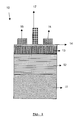
- Figure 1 represents a HEMT device in accordance with the present invention
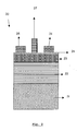
- Figure 2 represents an AlGaN/GaN based HEMT
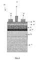
- Figure 3 represents an AlGaN/AlN/GaN based HEMT
- Figure 4 represents a GaN/AlGaN/AlN/GaN based HEMT
- Figure 5 represents an AlGaN/GaN based HEMT
- Figure 6 represents a method for forming a HEMT device
- Figure 7 represents a method for forming an AlGaN/GaN based HEMT device
- Figure 8 represents Transfer Length Measurements for uncapped and capped HEMT structures at three different temperatures
- Figure 9 represents DC drain source current-voltage characteristics for different gate bias voltages.
- the present invention describes a device and method that overcomes the problems related to surface stability and homogeneity, as well as a better control of the ohmic contact formation.
- the present invention is based on the surprising discovery that the ohmic contacts (source and drain contacts) are not hindered (and to the contrary are improved) by the presence (immediately underneath) of a SiN layer.
- a semiconductor device comprising:
- the term "on” when referring to the relative position of two layers can mean “directly or immediately on” (i.e. without an intermediary layer) or can also mean “above, with one or more intermediary layers”.
- said source and drain contacts are (deposited) directly on said passivation layer, i.e. there is no intermediary layer (neither between said source contact (or source electrode) and said passivation layer nor between said drain contact (or drain electrode) and said passivation layer).
- said electron donating element can be B, Se, or or C or Ge , but is preferably Si.
- said electron donating element in particular Si diffuses in said second active layer and acts there as a donor ; and the introduction of a donor type in said second active layer facilitates the ohmic contact formation reducing thereby the contact resistance.
- said passivation layer can comprise (or consist of) CN, BN, GeN, or SiN.
- said passivation layer comprises (or consists of) BN or SiN.
- said passivation layer comprises (or consists of) SiN.
- said passivation layer has a thickness comprised between (about) 1 nm and (about) 30 nm.
- said first active layer comprises (or consists of) a group III nitride semiconductor material, more particularly comprises (or consists of) GaN.
- said second active layer comprises (or consists of) a group III nitride semiconductor material, more particularly comprises (or consists of) AlGa or AlGaInN.
- a semiconductor device of the invention can further comprise a gate contact in electrical contact with said second active layer.
- a semiconductor device of the invention can further comprise a spacer layer between said first active layer and said second active layer.
- Said spacer layer aims at increasing the mobility in said 2DEG layer.
- said spacer layer can comprise (or consists of) AlN.
- a semiconductor device of the invention can further comprise a third layer between said second active layer and said passivation layer.
- Said third layer aims more particularly at providing electrons to the channel.
- said third layer comprises (or consists of) a group III nitride material.
- said substrate can comprise (or consist of) a material selected from the group consisting of silicon, sapphire, SiC, GaN and AlN.
- the present invention also provides a method for fabricating a semiconductor device comprising the steps of:
- said steps of depositing said first, second active layers and said passivation layer are performed in said reaction chamber without subjecting the layers to air or environment.
- a method of the invention further comprises, before the step of depositing the source and drain contacts, the steps of:
- said reaction chamber can be a MOVPE or a MBE reaction chamber.
- a method according to the invention can further comprise the step of forming a gate contact in electrical contact with said second active layer.
- Said gate contact can be deposited directly on said passivation layer (i.e with no intermediary layer).
- said passivation layer can be etched, in the channel region, in other words between the source and drain contacts. Said source and drain contacts remain directly on said passivation layer.
- a method of the invention can thus further comprise, after the step of depositing said source and drain contacts directly on said passivation layer, and before the step of forming said gate contact, the step of etching, between said source and drain contacts, said passivation layer.
- said step of depositing said passivation layer is performed at a temperature comprised between (about) 700°C and (about) 1300°C .
- Said passivation layer can comprise (or consist of) CN, BN, GeN or SiN.
- said passivation layer comprises (or consists of), BN or SiN.
- said passivation layer comprises (or consists of) SiN.
- said passivation layer is deposited to obtain a thickness comprised between (about) 1 nm and (about) 30 nm.
- said first active layer comprises (or consists of) a group III nitride semiconductor material, more particularly comprises (or consists of) GaN.
- said second active layer comprises (or consists of) a group III nitride semiconductor material, more particularly comprises (or consists of) AlGaN or AlGaInN.
- a method of the invention can further comprise the step of depositing a spacer layer between said first active layer and said second active layer.
- Said spacer layer aims more particularly at increasing mobility in said two-dimensional electron gas layer.
- said spacer layer comprises (or consists of) AlN.
- a method of the invention can further comprise the step of depositing a third layer between said second active layer and said passivation layer.
- Said third layer can be used for doping purposes or for increasing the carrier density in the channel.
- said third layer comprises (or consists of) a group III nitride semiconductor material, more particularly comprises (or consists of) GaN.
- a method of the invention can further comprise the step of depositing a buffer layer between said substrate and said first active layer.
- Said buffer layer aims at providing an appropriate crystal structure transition between said substrate and the other layers.
- said buffer layer comprises (or consists of) a group III nitride semiconductor material, and more particularly comprises (or consists of) AlN, GaN, AlGaN , InGaN and/or AlInGaN,
- said substrate comprises (or consists of) a material selected from the group consisting of silicon, sapphire, SiC, GaN and AlN.
- a method according to the invention can be used for fabricating a group III-N field effect device, and more particularly for fabricating a HEMT, MOSHFET, MESFET, MISFET, or MISHFET device.
- the present invention further provides a semiconductor device obtainable by a method according to the invention.
- FIG. 1 shows a HEMT device in accordance with the present invention.
- the HEMT device (10) comprises:
- the device can further comprise a gate (17) contact in electrical contact with the second active layer.
- a passivation layer is deposited on the second active layer in-situ, at high temperature, in the MOCVD reactor chamber, prior to cooling down the structure and exposing the top surface to air contamination.
- the formation of the transistor, in particular the contact deposition, is then performed without any removal of the passivation layer prior to contact deposition, notably for the ohmic contact.
- MOVPE growth of such heterostructures followed by the preparation of high electron mobility transistors on top of those heterostructures, with the technique suggested, allows for better performance of the transistor: higher current density, higher power performance compared to: (a) transistors prepared without any passivation, (b) transistors prepared with in-situ passivation or ex-situ between the drain and the source, (c) transistors prepared with in-situ passivation and removal of the passivation layer below the ohmic contacts. As an example, it allows for doubling of the current density, compared to a transistor prepared with ex-situ deposition of the passivation layer between the drain and source, which is actually the most widely used technique to develop group III-nitride devices nowadays.
- In-situ passivation prevents any contamination of the surface prior to processing such that no oxidation of the surface of the second active layer occurs.
- the passivation is deposited in-situ at high temperature, close to growth temperature, prior cooling down, it experiences the same cooling down step as the overall structure.
- the cooling down from growth temperature is thus different with and without the presence of the passivation layer.
- the presence of passivation layer allows increasing the Al content in the layer, without any cracking of the wafer. This allows for an increase of the 2DEG concentration.
- improvement of the quality of ohmic contact formation of the device lower contact resistance, very linear I-V characteristics, sheet resistances in agreement with material properties obtained by Hall measurement, showing that the total current capabilities which are present within the channel, can be extracted through the contacts.
- Deposition of the passivation layer allows for a better ohmic contact formation, with better control of uniformity over a wafer and reproducibility from one wafer to another, by passivating the surface and offering a better control of the surface states, as well a of the strain in the heterostructure, which is entirely controlled during MOVPE growth.
- Figure 2 represents an AlGaN/GaN based HEMT (20) in accordance with the present invention.
- the HEMT comprises a substrate (21).
- the substrate can be sapphire, SiC, Si or GaN.
- the substrate can comprise a nucleation layer on the substrate to accommodate for the change in crystal parameters between substrate and layer.
- a buffer layer can also be included on the substrate to provide for an appropriate crystal structure transition between the substrate and the remainder of the HEMT.
- the HEMT (20) comprises a GaN (22) layer on the substrate and an AlGaN (23) layer on the GaN layer such that the GaN layer is sandwiched between the substrate and the AlGaN layer.
- the GaN layer is typically between 1000 and 3000 nm thick, between 2000 and 3000 nm thick while the AlGaN layer is between 10 nm and 50 nm thick, or between 10 nm and 40 nm thick.
- This top structure can be made of a single AlGaN layer, n-type doped or undoped, or a set of different layers doped or undoped layers, to increase confinement for the two-dimensional-electron gas.
- the Al content can vary between 10% and 100%.
- the GaN layer and the AlGaN layer are typically formed by MOCVD.
- the HEMT (20) further comprises a passivation layer (24) on the AlGaN layer.
- the passivation layer covers the entire AlGaN layer or can partially cover the AlGaN layer. At least the regions where the source contact and the drain contact are formed should be covered by the passivation layer.
- the passivation layer comprises at least an electron donating element and nitrogen.
- the passivation layer can be made of SiN or AlN or a combination including multiple layers of SiN and AlN.
- the AlGaN layer has a higher bandgap than the GaN layer.
- surface charged layers could be created in the device.
- the surface charged layers are compensated by the formation of two-dimensional electron gas at the other side of the interface, resulting in high mobility values compared to the bulk material. This is beneficial for the creation of very high electron mobility channel in the device.
- the HEMT further comprises a source contact (25) and a drain contact (26) on the passivation layer.
- the source contact and the drain contact are made of metals, preferably an alloy of different metals, which are deposited as layers and then annealed.
- the metals can be selected from the group consisting Ti, Al, Ni, Mo, Ta, Pt, Pd, V, Nb, Zr and/or Au.
- the gate contact (27) is preferably formed of a material selected from the group consisting of Ti, Pt, Cr, Ni, Mo, Co, Au and Pd, combination thereof and alloys thereof.
- the drain contact is biased at a predetermined potential while the source contact is grounded. Consequently, current will flow from the source to the drain in the channel and the 2DEG.
- the current flow is controlled by the bias and the potential applied to the gate electrode.
- Figure 3 represents an AlGaN/AlN/GaN based HEMT (30) similar to the HEMT (20) in Figure 2.
- the HEMT has similar layers comprising a substrate (31), an AlGaN layer (32), a GaN layer (33) and a passivation layer (34).
- the HEMT comprises a source electrode (35), a drain electrode (36) and a gate electrode (37).
- the HEMT (30) further comprises an AlN layer (38) disposed on the AlGaN layer between the AlGaN layer and the GaN layer.
- the AlN layer allows to obtain a higher bandgap, thus a more narrow 2DEG channel en less penetration of the wavelfunction in the AlGaN layer, resulting in reduced scattering (reducing effect of interface roughness) thus increasing the mobility.
- Figure 4 represents a GaN/AlGaN/AlN/GaN based HEMT (40) similar to the HEMT (20) in Figure 2.
- the HEMT has similar layers comprising substrate (41), an AlGaN layer (42), a GaN layer (43) and a passivation layer (44).
- the HEMT (40) further comprises an AlN layer (48) disposed on the AlGaN layer between the AlGaN layer and the GaN layer.
- the HEMT (40) further comprises a GaN layer (49) on top op the AlGaN layer.
- the passivation layer is deposited on top of the GaN layer.
- the GaN layer can prevent oxidation of the AlGaN layer.
- Figure 5 represents a AlGaN/GaN based HEMT (50) similar to the HEMT in Figure 2.
- the HEMT has similar layers comprising a substrate (51), an AlGaN layer (52) and a GaN layer (53).
- the HEMT comprises a source electrode (55), a drain electrode (56) and a gate electrode (57).
- the gate contact is in direct contact with the AlGaN layer, meaning that no passivation layer (54) is present between the gate contact and the Al GaN layer.
- Figure 6 shows a method for forming a HEMT device, the method comprising the steps of :
- the method can further comprise the step of forming a gate contact in electrical contact with said second active layer (66).
- the gate contact is formed on the uncovered part of the passivation layer. This step is optional.
- the steps of forming a first active layer, forming a second active layer and forming a passivation layer are performed in a MOCVD reactor chamber in a continuous process, meaning without subjecting the device to the air (for the purpose of this invention also called "in situ" formation).
- the formation of an oxide on the second active layer is substantially avoided.
- the step of removing the oxide layer from the top surface of the second active layer is avoided. This results in an improved ohmic contact formation.
- the prior art shows that the oxide which spontaneously forms over the top surface of the second active layer is very stable, and thus requires high power and/or high duration of plasma etching prior effectively eliminating the oxide layer.
- Figure 7 represents a method for forming an AlGaN/ GaN HEMT device in accordance with the present invention.
- the AlGaN/GaN structures were grown by Metal-Organic Vapor Phase Epitaxy (MOVPE) on [0001] sapphire substrates.
- Starting compounds are trimethylgallium (TMGa), trimethylaluminium (TMAl), ammonia (NH 3 ) and silane (SiH 4 , 200 ppm in hydrogen).
- the silane introduction line is modified in such a way that the amount of silane introduced in the reactor can be regulated from about 5 nmol/min up to about 1 ⁇ mol/min.
- the substrates are annealed in H 2 at 1050° C at 53,33 mbar (40 torr). Then, nitridation of the surface is carried out at 800°C by introducing NH 3 into the reactor. After that, the substrates are cooled down to 525°C and a thin nucleation layer is grown (78) at 533,3 mbar (400 torr) by introducing TMGa into the reactor during 120 seconds. Subsequently, the temperature is ramped to 1020°C and at a pressure of 133,3 mbar (100 torr) GaN is grown to a thickness of 2.6 microns (72).
- the growth is interrupted during 30 seconds while the reactor pressure is decreased to 53,33 mbar (40 torr).
- an AlN spacer layer (77) is grown followed by an Al x Ga 1-x N layer (73) of thickness 20 to 22 nm.
- the group III compound source is stopped, while keeping the NH 3 flow to the reactor and opening the SiH 4 line, allowing for growth of SiN at high temperature (74)
- the SiH 4 flow is stopped and the structure is cooled down to room temperature while keeping the NH 3 flow, to avoid desorption from the top layer.
- the wafers are unloaded out of the reactor. The surface is very well protected by the SiN passivation layer.
- steps 75 and 76 The processing of transistors (steps 75 and 76) on such structures is similar to the process described above.
- AlGaN/GaN HEMT structures are grown at low pressure (133,3 mbar (100 Torr)) using Metal Organic Vapour Phase Epitaxy (MOVPE).
- MOVPE Metal Organic Vapour Phase Epitaxy
- trimethyl gallium (TMGa), trimethyl alminium (TMAl) and ammonia (NH 3 ) are used.
- the metal-organic precursors are transported with hydrogen as carrier gas; the amounts are regulated by means of mass flow controllers and the temperature of the thermostat baths in which the metal organic bubblers are mounted.
- the flow of ammonia is also regulated by means of a mass flow controller and traces of water and oxygen are removed by an in-line filter.
- n-type doping of the GaN and (Al,Ga)N layers can be achieved by adding silane (SiH 4 ) during growth.
- a thin GaN buffer layer is deposited at lower temperature using NH 3 and TMGa.
- the substrate temperature is then set to 1020C and a 2 micrometer thick semi-insulating GaN layer is grown.
- the pressure is lowered to 53,33 mbar (40 T)
- the temperature is raised to 1050°C and Al flow is sent to the reactor for deposition of Al x Ga 1-x N, with x included (comprised) between 20% and 40%.
- Typical thickness of AlGaN is 25 nm.
- the sources for III-type elements are then sent to the vent and SiH 4 is introduced in the reactor, simultaneously with NH 3 , at the same pressure and temperature conditions as for AlGaN growth.
- SiN grows from NH 3 and SiH 4 at a growth rate of around 6nm/h.
- the SiN layer can also be grown at a growth rate of 0.3 ⁇ /h.
- Transistors have then been prepared on these structures using standard processing, without any etching of the top SiN layer.
- Transfer Length method show a reduction of the ohmic contact resistance but also a large improvement of the I-V characteristic uniformity, giving sheet resistivity values in fair agreement with Hall measurements.
- Spectacular improvement of the dc characteristics is observed: drain-source current measurements for a positively biased gate (2V) show an increase of more than a factor two in current density from 0.5 A/mm in the reference sample to 1.2 A/mm with in-situ passivation, for a device width of 100 ⁇ m and a gate length of 0.2 ⁇ m.
- RF measurements show a f t of 40 GHZ and f max of 80 GHz, for the same device geometry. This is an increase in current density compared to results obtained with ex-situ SiN passivation. Further an improvement of DC and RF properties is observed.
- the AlGaN/GaN HEMT structures were grown by MOVPE on [0001] sapphire substrates.
- a Thomas Swan close-coupled showerhead reactor was used with starting compounds trimethylgallium (TMGa), trimethylaluminium (TMAl), ammonia (NH 3 ) and diluted silane (SiH 4 , 200 ppm in hydrogen).
- the silane introduction line is modified in such a way that the amount of silane introduced in the reactor can be regulated from the required amount for n-type doping of GaN (a few nmol/min up) to about 1 ⁇ mol/min.
- a 2.6 ⁇ m thick GaN layer is grown at 1020°C with a reactor pressure 133,3 mbar (100 Torr).
- a thin AlN spacer layer is grown at 53,33 mbar (40 Torr) to improve mobility in the 2DEG.
- the top AlGaN layer is 22 to 24 nm thick and the Al content is 30 % as determined by High-Resolution X-Ray Diffraction measurements.
- the reactor was purged during 10 seconds while maintaining the NH 3 flow. Then silane was introduced. Results on SiN thickness ranging from 3.5 to 15 nm are presented.
- Transistors have been processed on these heterostructures. For the sake of comparison, similar structures without the in-situ grown SiN protecting layer have also been processed using the same technology, simultaneously.
- Ti/Al/Pt/Au contacts were deposited on the SiN top layer, without any etching of the passivating layer and followed by rapid thermal annealing.
- Electron-beam lithography is used to pattern the gate Ni/Au Schottky contacts, to a dimension of 0.2 ⁇ m.
- TLM Transfer Length Method
- the TLM measurements performed on uncapped HEMT structure (without SiN passivation layer) (81 at 820°C , 82 at 860°C , 83 at 900°C) give a best ohmic contact resistance of 1.49 ⁇ mm.
- the slope of the TLM line which gives the sheet resistance, is different and varies between 395 and 528 ⁇ /sq.. These values are moreover higher than the sheet resistance value determined by Hall or by contact-less sheet resistivity measurements ( ⁇ /sq.).
- TLM measurements performed on the capped SiN epiwafers display a single sheet resistance value, in fair agreement with the other determinations of the sheet resistance values.
- the ohmic contact resistance reduces to a value of 0.88 ⁇ mm, for a similar ohmic contact deposition scheme.
- the DC drain source current-voltage characteristics for different gate bias voltages are given in Figure 9, for a device width of 100 ⁇ m and gate length of 0.2 ⁇ m; similar HEMT structure have been processed, one having no SiN passivation layer (also called uncapped) (a) and the other HEMT having a SiN passivation layer between the ohmic contacts and the AlGaN layer (also called capped in-situ), the passivation layer being a 7 nm thick SiN layer) (b).
- the measurements show an improvement of more than a factor two in current density from 0.5 A/mm to 1.2 A/mm.
- f t and f max are respectively 24 GHz and 68 GHz, whereas for the in-situ passivated one, they give a ft of 40 GHz and f max of 80 GHz.
Abstract
Description
- The invention relates to the group III-nitride field effect devices, and methods to improve stability of the surface, by passivation of the top surface, as well as to ohmic contact deposition on wide bandgap layers.
- GaN Field-effect devices are piezoelectric devices, i.e. the presence of spontaneous and piezoelectric polarizations are responsible for charge separation within the material.
- This has the enormous advantage that it allows, at the interfaces between different material composition, e.g. AlGaN and GaN, the creation of surface charged layers in the structures. Those surface charged layers are compensated in the AlGaN/GaN junction by the formation of two-dimensional electron gas (2DEG) at the other side of the interface, which has high mobility values compared to the bulk material. If necessary and beneficial for the creation of very high mobility channel in the structure, allowing for demonstration of high power HEMT devices, it has the drawback that the separation charges within wurtzite material, is also responsible for the surface charged layer at the top surface of the structure, leading to an increased importance of surface states, compared to zincblend structure materials. Presence of surface states creates acute problems for achieving the high performance that are theoretically predicted for those devices, as surface states play an important role during device operation. It has been noticed by many authors that the reduction of dc performance, current slump at high drain-source voltages, DC to RF dispersion phenomena, are directly related to the filling, emptying of surface states, although thermal effects are also partially responsible for dc current slump.
- To minimize the effect of such surface states on the top III-N structures, passivation of the surface between drain and source by e.g. SiN, SiO2, has been proposed by different authors, using essentially ex-situ methods, during the processing of the transistors. These methods are very dependent on the growth conditions of the oxide or insulating layer on the top surface, as strain effects, tuned by growth conditions and also dependent on the strain state in the heterostructure itself, also have a influence on the two-dimensional electron gas properties. They are also very dependent on the chemical or mechanical state of the surface, which is depending on the previous processing steps that have occurred on this top surface.
- US 2003/0020092 A1 describes an AlGaN/GaN HEMT having a thin AlGaN layer. Source and drain contacts contact the AlGaN layer, while parts of the AlGaN layer being uncovered by the contacts. An insulating layer covers the uncovered part of the AlGaN layer and a gate contact is included on the insulating layer. In an embodiment, the HEMT and the insulating layer are fabricated using metal-organic chemical vapor deposition. In another embodiment, the insulating layer is sputtered onto the top surface of the HEMT active layers.
- WO 01/13436 A1 describes a GaN based FET that employs dielectric passivation layers on exposed AlGaN or GaN surfaces of the devices above the channel regions, between the source and drain contacts. The dielectric layer is formed of SiN. The layer controls undesirable frequency-dependent current and reduced breakdown voltage.
- US 5,192,987 recites a high electron mobility transistor. The transistor consists of a GaN/AlGaN heterojunction, where a two-dimensional electron gas occurs. The structures are deposited on basal plane sapphire using low-pressure metal organic chemical vapor deposition.
- Another problem in the development of field-effect GaN based transistors is the ohmic contact formation on the group III-nitride surface. The ohmic contact formation is dependent on different factors, e.g. the surface composition, but one very important, which has long been underestimated, is the degree of oxidation of the top surface. Different cleaning techniques and metallization techniques have been suggested to overcome this problem. The lack of a good ohmic contact formation on the top layer directly leads to drastic reduction of the device performance. It is very often observed that the maximum current which is measured, under dc conditions, is well below the maximum current density values deduced from material considerations such as carrier density and mobility in the channel.
- Furthermore, the uniformity and reproducibility of the device performances over a wafer and from wafer to another is often a problem. Even if record performance has been demonstrated on selected HEMT devices, uniformity and reproducibility of the results remain problematic. Although improvement of material quality and device processing is believed to allow for better results in uniformity and reproducibility, a fundamental problem to be overcome is the accurate control of the surface properties.
- Finally, another problem, frequently encountered with piezeoelectric devices such as AlGaN/GaN HEMT devices is the following. In order to increase the current density in the two-dimensional electron gas, there exist two possibilities: either increase the AlGaN layer thickness, or increase the Al content in this top surface. These two possibilities, by increasing the strain in the top AlGaN, which is grown pseudomorphically on the GaN layer, leads to an increased carrier density in the channel. However, the presence of high strain in the AlGaN layer rapidly leads to cracking of this top surface. Those cracks in the AlGaN are very prejudicial, they destroy the 2DEG at the AlGaN/GaN interface; second, they complicate processing. It would therefore be interesting to find a possibility of preventing crack appearance in the top AlGaN, even for highly strained layers. It is important to note that most of these cracks are believed to occur during the cooling down of the structure. An effective way of reducing cracks appearance in III-N devices is even more highly demanded when growing these III-N devices on Si substrates, as differences in thermal expansion coefficients are even larger than with SiC or sapphire substrates.
- It is an aim of the invention to stabilize the surface of the GaN field-effect devices prior surface contamination by air exposure and any damaging through different processing steps, in order to have an increased electron density in the channel and a high performance device, as well as a reliable process.
- It is a further aim to have a reduced ohmic contact resistance.
- It is a further aim of the invention to increase the two-dimensional electron gas, by reducing the strain-induced modification during cooling down, by allowing for higher strain in the heterostructure without damaging the mechanical properties of the top surface and thus directly increase the HEMT performance
- In a first aspect of this invention, a device is recited, the device comprising
- a substrate,
- a first active layer,
- a second active layer on said first active layer, said second active layer having a higher bandgap than said first active layer,
- a two-dimensional electron gas layer between said first active layer and said second active layer,
- a passivation layer on said second active layer,
- a source contact and a drain contact, said source contact and said drain contact contacting said passivation layer.
- In a device of the invention, the passivation layer can be arranged such that the electron density in the two-dimensional electron-gas layer is increased.
- In a device of the invention, the gate contact is preferably in electrical contact with said second active layer.
- In a device of the invention, said first active layer is preferably formed of a group III nitride semiconductor material, more particularly of GaN.
- In a device of the invention, the second active layer is preferably formed of a group III nitride semiconductor material, more particularly of AlGaN or AlGaInN.
- In a device of the invention, a spacer layer can be positioned between the first active layer and the second active layer.
- In a device of the invention, a third layer, preferably formed of a group III nitride material, can be positioned between said second active layer and said passivation layer.
- More particularly, in a device of the invention, said passivation layer can be arranged such that it reduces or eliminates the effect of surface states on the carrier density in the two-dimensional electron gas, during device operation.
- In a device of the invention, said passivation layer is preferably formed of a material comprising at least an electron donating element and nitrogen, more particularly is formed of silicon nitride.
- In a device of the invention, the passivation layer can be a multi-layered structure comprising a group III nitride material and a material selected from the group consisting of SiN or AlN.
- In a device of the invention, the thickness of the passivation layer is preferably between 1 nm and 30 nm.
- In a device of the invention, the substrate is preferably formed of a material selected from the group consisting of silicon, sapphire, SiC, GaN and AlN.
- In an embodiment of this invention, the source contact and the drain contact are deposited on the passivation layer.
- In an embodiment of this invention, a device as recited in the previous embodiments is disclosed further comprising a gate contact in electrical contact with said second active layer.
- In another embodiment, a part of said passivation layer is being uncovered by the source contact and the drain contacts. The gate contact can contact the passivation layer or the gate contact can be deposited on the second active layer.
- In another embodiment, a device as recited in any of the previous embodiments is disclosed wherein the first active layer is formed of a group III nitride semiconductor material.
- In a preferred embodiment, the first active layer is formed of GaN.
- In another embodiment, said second active layer is formed of a group III nitride material.
- In a preferred embodiment, the second active layer is formed of AlGaN or AlGaInN.
- Between the first active layer and the second active layer (also called the interface), surface charged layers could be created in the device. The surface charged layers are compensated by the formation of two-dimensional electron gas at the other side of the interface, resulting in high mobility values compared to the bulk material. This is beneficial for the creation of a very high mobility channel in the device.
- In another embodiment, a spacer layer is present between the first active layer and the second active layer. The spacer layer is selected such that the mobility at the interface is increased.
- The spacer layer can be formed of, but is not limited hereto, AlN.
- In another embodiment, the second active layer is partly or entirely doped with donor elements such as Si, to provide another source of electrons.
- In another embodiment, the second active layer is covered by a third layer, the third layer being formed of a Group III nitride material such as, but not limited hereto, GaN. The third layer is between the second active layer and the passivation layer.
- In another embodiment, the device can further comprise at least one buffer layer between the substrate and the first active layer. The buffer layer provides an appropriate crystal structure transition between the substrate and the remainder of the device. The buffer layer can be a nucleation layer between the substrate and the first active layer. In a particular embodiment, the buffer layer can consist of, but is not limited hereto, AlN, GaN or AlGaN.
- In an embodiment of the invention, the passivation is arranged such that it reduces or eliminates the effect of surface states on the carrier density in the two-dimensional electron gas, during device operation.
- In an embodiment of the invention, a device as recited in any of the previous embodiments is disclosed wherein said passivation layer comprises at least a donor material and nitrogen.
- In a particular embodiment, the passivation layer is formed of silicon nitride.
- In another embodiment, the passivation layer is formed of Magnesium nitride.
- In a further embodiment, the passivation layer is a multi-layered structure comprising a group III nitride material and a SiN or AlN.
- The passivation layer is arranged such that it reduces the effect of surface states on the carrier density in the two-dimensional electron gas, during device operation.
- Although the invention is not limited to this, a possible explanation of such an effect is that the SiN layer could provide a charge neutral interface with the AlGaN, eliminating surface depletion of the 2DEG. The presence of high level of Si or at least donor-type of defects in the passivation layer could be are beneficial for the compensation of surface charge effects. Presence of surface states creates accurate problems for achieving the high performance, as surface states play an important role during device operation.
- The thickness of the passivation layer is between 1 nm and 100 nm, between 1 nm and 50 nm, between 1 nm and 30 nm, or between 1 nm and 20 nm. Preferably, the thickness is between 1 nm and 30 nm.
- The passivation layer is characterized by an amorphous structure.
- Furthermore, a thin passivation layer allows the formation of ohmic contacts with a low resistance.
- Furthermore, the passivation layer comprises Si, the Si can diffuse in the AlGaN, where it acts as a donor.
- The introduction of a donor type in the AlGaN layer facilitates the ohmic contact formation reducing thereby the contact resistance.
- The first active layer, the second active layer and the passivation layer are formed in the same reactor without subjecting the layers to air.
- Preferably, the passivation layer is formed by MOVPE (Metal-Organic Vapor Phase Epitaxy) or MBE (Molecular Beam Epitaxy).
- The passivation layer is formed at a temperature between 700°C and 1300 °C, between 700 °C and 1250 °C, between 700 °C and 1100°C.
- In a further embodiment, the second active layer is not covered with an oxide layer. The passivation layer is in direct contact with the second active layer.
- In a further embodiment, a device as recited in any of the previous embodiments is disclosed wherein the substrate is formed of a material selected from the group consisting of silicon, sapphire, SiC, GaN and AlN.
- In another embodiment of the present invention, the device as recited in any of the previous embodiments is a field-effect transistor. The field-effect transistor can be, but is not limited hereto, a HEMT (High Electron Mobility Transistor), MOSHFET (Metal Oxide Semiconductor Heterostructure Field Effect Transistors), MESFET (Metal Semiconductor Field Effect Transistor), MISFET (Metal-Insulator-Semiconductor Field Effect Transistor), or MISHFET (Metal-Insulator-Semiconductor Heterostructure Field Effect Transistor).
- In a further embodiment, the device as recited in any of the previous embodiments is disclosed wherein the device is characterized by a higher current density and a higher power performance compared to prior art devices.
- In another preferred embodiment, the source contact and drain contact are made of an alloy comprising Ti, Al, Ni, Mo, Ta, Pt, Pd, V, Nb, Zr and/or Au. The contact being preferably formed by Ti/Al/Ti/Au sequence, Ti/Al/Ni/Au, Ti/Al/Mo/Au or Ti/Al/Pt/Au.
- It is probable that, when one of the layers is made of Al, the latter easily forms an alloy with nitrogen, AlN, and that silicon acts as a dopant in the AlGaN layer. This facilitates the ohmic contact formation.
- In a second aspect of this invention, a method for forming a device is recited, the method comprising the steps of:
- placing a substrate in a reaction chamber
- forming a first active layer on said substrate
- forming a second active layer on said first active layer, said second active layer having a higher bandgap than said first active layer, thereby forming a two-dimensional electron gas layer between said first active layer and said second active layer,
- forming a passivation layer on said second active layer
- forming a source contact and a drain contact, said source contact and said drain contact contacting said passivation layer, with part of said passivation layer being uncovered by the source contact and the drain contact.
- A method according to the invention may further comprise the step of forming a gate contact in electrical contact with said second active layer.
- In a method of the invention, the steps of forming a first active layer, forming a second active layer and forming a passivation layer are performed in a reactor chamber without subjecting the device to the air (environment).
- More particularly, said reaction chamber can be a MOVPE (Metal Organic Vapour Phase Epitaxy) reaction chamber.
- A method of the invention may further comprise the steps of:
- cooling said reaction chamber,
- removing said device with its deposited layers from said reaction chamber,
- In a method of the invention, the step of forming the passivation layer is preferably performed at a temperature between 700°C and 1300 °C.
- In a method of the invention, the steps of forming a source contact and drain contact are performed such that there is a direct contact between the passivation layer and the source contact and the drain contact.
- In a method of the invention, the first active layer is preferably formed of a group III nitride semiconductor material, more particularly of GaN.
- In a method of the invention, the second active layer is preferably formed of a group III nitride semiconductor material, more particularly of AlGaN or AlGaInN.
- In a method of the invention, the passivation layer preferably comprises an electron donating element and nitrogen, more particularly said passivation layer is made of SiN.
- In an embodiment of the second aspect of this invention, a method as recited in any of the previous embodiments is disclosed further comprising the step of forming a gate contact in electrical contact with said second active layer. The gate contact is formed on the uncovered part of the passivation layer.
- In an embodiment of the second aspect of this invention, the steps of forming a first active layer, forming a second active layer and forming a passivation layer are performed in a reactor chamber without subjecting the device to the air (for the purpose of this invention also called "in situ" formation).
- In a preferred embodiment, the reaction chamber is a MOVPE reaction chamber.
- The formation of an oxide on the second active layer is substantially avoided. Moreover, the step of removing the oxide layer from the top surface of the second active layer is avoided. This results in an improved ohmic contact formation.
- The prior art shows that the oxide which spontaneously forms over the top surface of the second active layer is very stable, and thus requires high power and/or high duration of plasma etching prior effectively eliminating the oxide layer.
- In another embodiment of the second aspect of this invention, the method can further comprise the step of forming at least one buffer layer between the substrate and the first active layer.
- This step is performed after the step of placing the substrate in the reaction chamber.
- The buffer layer provides an appropriate crystal structure transition between the substrate and the remainder of the device.
- The buffer layer can be a nucleation layer between the substrate and the first active layer.
- In a particular embodiment, the buffer layer can consist of, but is not limited hereto, AlN, GaN, AlGaN or InN or combinations thereof.
- In a particular embodiment, the buffer layer is formed at a growth temperature which is lower than the growth temperature of the first active layer.
- In another embodiment of the second aspect of this invention, the method further comprises the step of:
- cooling said reaction chamber
- removing said device with its deposited layer from said reaction chamber,
- In another embodiment, the step of forming the passivation layer is performed at a temperature between 700°C and 1300 °C, between 700 °C and 1250 °C, or between 700 °C and 1100°C.
- The passivation layer being deposited at least at 700° C on top of the second active layer, preferably AlGaN, results in a reduction of the cracks in the second active layer. Cracks occur when cooling down the device from growth temperature to room temperature. Therefore, it allows increasing either the thickness of the second active layer, and/or the Al content in the second active layer. This results in an increase of the carrier density in the channel.
- The step of forming a source contact and drain contact are performed such that there is a direct contact between the passivation layer and the source contact and the drain contact. This means that the passivation layer is not etched before formation of the source and drain contacts.
- It should be understood that when SiN is mentioned, a compound consisting of Si and N is meant. SiN can include Si3N4, but also other formulas are included, such as, but not limited hereto, SixNy, being in different stoichiometric or non-stoichiometric ratios.
- In the formula SixNy, x and y can be defined as real numbers, with 0 < x ≤ 100 and 0 < y ≤ 100.
- In an embodiment of the second aspect of this invention, the step of forming a first active layer comprises flowing source gasses adapted for the formation of the first active layer into a reactor chamber. The step of forming a second active layer comprises flowing source gases adapted for the formation of the second active layer into said reaction chamber. The step of forming the passivation layer comprises flowing source gasses adapted for the formation of the passivation layer into a reactor chamber.
- In a further embodiment, the first active layer is formed of a group III nitride semiconductor material. In a preferred embodiment, the first active layer is formed of GaN. In another further embodiment, said second active layer is formed of a group III nitride material. In a preferred embodiment, the second active layer is formed of AlGaN.
- In another further embodiment, said passivation layer is formed of silicon nitride.
- The specifications of the different layers formed by the method are similar to those described in the first aspect of the invention.
- Figure 1 represents a HEMT device in accordance with the present invention
- Figure 2 represents an AlGaN/GaN based HEMT
- Figure 3 represents an AlGaN/AlN/GaN based HEMT
- Figure 4 represents a GaN/AlGaN/AlN/GaN based HEMT
- Figure 5 represents an AlGaN/GaN based HEMT
- Figure 6 represents a method for forming a HEMT device
- Figure 7 represents a method for forming an AlGaN/GaN based HEMT device
- Figure 8 represents Transfer Length Measurements for uncapped and capped HEMT structures at three different temperatures
- Figure 9 represents DC drain source current-voltage characteristics for different gate bias voltages.
- The present invention will be described with respect to particular embodiments and with reference to certain drawings but the invention is not limited thereto but only by the claims. The drawings described are only schematic and are non-limiting. In the drawings, the size of some of the elements may be exaggerated and not drawn on scale for illustrative purposes
- The present invention describes a device and method that overcomes the problems related to surface stability and homogeneity, as well as a better control of the ohmic contact formation.
- The present invention is based on the surprising discovery that the ohmic contacts (source and drain contacts) are not hindered (and to the contrary are improved) by the presence (immediately underneath) of a SiN layer.
- A semiconductor device is provided comprising:
- a substrate,
- a first active layer,
- a second active layer (on said first active layer), said second active layer having a higher bandgap than said first active layer,
- a two-dimensional electron gas layer between said first active layer and said second active layer,
- a passivation layer (on said second active layer) consisting of an electron donating element and nitrogen,
- a source contact and a drain contact directly deposited on said passivation layer.
- In the context of the present invention and except if specified otherwise, the term "on" when referring to the relative position of two layers, can mean "directly or immediately on" (i.e. without an intermediary layer) or can also mean "above, with one or more intermediary layers".
- In particular, in a semiconductor device or in a method according to the invention, said source and drain contacts are (deposited) directly on said passivation layer, i.e. there is no intermediary layer (neither between said source contact (or source electrode) and said passivation layer nor between said drain contact (or drain electrode) and said passivation layer).
- In a semiconductor device according to the invention, said electron donating element can be B, Se, or or C or Ge , but is preferably Si.
- It is probable that said electron donating element (in particular Si) diffuses in said second active layer and acts there as a donor ; and the introduction of a donor type in said second active layer facilitates the ohmic contact formation reducing thereby the contact resistance.
- It is also probable that, when one of the layers is made of Al, the latter easily forms an alloy with nitrogen, AlN, and that said electron donating element (in particular Si) acts as a dopant in the AlGaN layer. This facilitates the ohmic contact formation.
- In a semiconductor device according to the invention, said passivation layer can comprise (or consist of) CN, BN, GeN, or SiN. Preferably, said passivation layer comprises (or consists of) BN or SiN. And more preferably, said passivation layer comprises (or consists of) SiN.
- Preferably, said passivation layer has a thickness comprised between (about) 1 nm and (about) 30 nm.
- Preferably, said first active layer comprises (or consists of) a group III nitride semiconductor material, more particularly comprises (or consists of) GaN.
- Preferably, said second active layer comprises (or consists of) a group III nitride semiconductor material, more particularly comprises (or consists of) AlGa or AlGaInN.
- A semiconductor device of the invention can further comprise a gate contact in electrical contact with said second active layer.
- A semiconductor device of the invention can further comprise a spacer layer between said first active layer and said second active layer. Said spacer layer aims at increasing the mobility in said 2DEG layer. For example, said spacer layer can comprise (or consists of) AlN.
- A semiconductor device of the invention can further comprise a third layer between said second active layer and said passivation layer. Said third layer aims more particularly at providing electrons to the channel. Preferably, said third layer comprises (or consists of) a group III nitride material.
- In a semiconductor device according to the invention, said substrate can comprise (or consist of) a material selected from the group consisting of silicon, sapphire, SiC, GaN and AlN.
- The present invention also provides a method for fabricating a semiconductor device comprising the steps of:
- placing a substrate in a reaction chamber,
- depositing on said substrate a first active layer,
- depositing on said first active layer a second active layer having a higher bandgap than said first active layer, thereby forming a two-dimensional electron gas layer between said first active layer and said second active layer,
- depositing on said second active layer a passivation layer comprising at least an electron donating element and nitrogen,
- depositing directly on said passivation layer a source contact and a drain contact.
- In a method of the invention, said steps of depositing said first, second active layers and said passivation layer are performed in said reaction chamber without subjecting the layers to air or environment.
- Preferably, a method of the invention further comprises, before the step of depositing the source and drain contacts, the steps of:
- cooling said reaction chamber, and
- removing the device (or structure) (with its deposited layers) from said reaction chamber.
- In a method of the invention, said reaction chamber can be a MOVPE or a MBE reaction chamber.
- A method according to the invention can further comprise the step of forming a gate contact in electrical contact with said second active layer.
- Said gate contact can be deposited directly on said passivation layer (i.e with no intermediary layer).
- Alternatively, said passivation layer can be etched, in the channel region, in other words between the source and drain contacts. Said source and drain contacts remain directly on said passivation layer. A method of the invention can thus further comprise, after the step of depositing said source and drain contacts directly on said passivation layer, and before the step of forming said gate contact, the step of etching, between said source and drain contacts, said passivation layer.
- Preferably, in a method of the invention, said step of depositing said passivation layer is performed at a temperature comprised between (about) 700°C and (about) 1300°C .
- Said passivation layer can comprise (or consist of) CN, BN, GeN or SiN. Preferably, said passivation layer comprises (or consists of), BN or SiN. And more preferably, said passivation layer comprises (or consists of) SiN.
- Preferably, said passivation layer is deposited to obtain a thickness comprised between (about) 1 nm and (about) 30 nm.
- Preferably, in a method of the invention, said first active layer comprises (or consists of) a group III nitride semiconductor material, more particularly comprises (or consists of) GaN.
- Preferably, in a method of the invention, said second active layer comprises (or consists of) a group III nitride semiconductor material, more particularly comprises (or consists of) AlGaN or AlGaInN.
- A method of the invention can further comprise the step of depositing a spacer layer between said first active layer and said second active layer. Said spacer layer aims more particularly at increasing mobility in said two-dimensional electron gas layer. Preferably, said spacer layer comprises (or consists of) AlN.
- A method of the invention can further comprise the step of depositing a third layer between said second active layer and said passivation layer. Said third layer can be used for doping purposes or for increasing the carrier density in the channel. Preferably, said third layer comprises (or consists of) a group III nitride semiconductor material, more particularly comprises (or consists of) GaN.
- A method of the invention can further comprise the step of depositing a buffer layer between said substrate and said first active layer. Said buffer layer aims at providing an appropriate crystal structure transition between said substrate and the other layers. Preferably, said buffer layer comprises (or consists of) a group III nitride semiconductor material, and more particularly comprises (or consists of) AlN, GaN, AlGaN , InGaN and/or AlInGaN,
- Preferably, in a method of the invention, said substrate comprises (or consists of) a material selected from the group consisting of silicon, sapphire, SiC, GaN and AlN.
- A method according to the invention can be used for fabricating a group III-N field effect device, and more particularly for fabricating a HEMT, MOSHFET, MESFET, MISFET, or MISHFET device.
- The present invention further provides a semiconductor device obtainable by a method according to the invention.
- Figure 1 shows a HEMT device in accordance with the present invention. The HEMT device (10) comprises:
- a substrate (11),
- a first active layer (12),
- a second active layer on said first active layer, said second active layer having a higher bandgap than said first active layer (13),
- a two-dimensional electron gas layer between said first active layer and said second active layer ,
- a passivation layer on said second active layer (14),
- a source contact (15) and a drain contact (16), said source contact and said drain contact contacting said passivation layer.
- The device can further comprise a gate (17) contact in electrical contact with the second active layer.
- In the present invention, a passivation layer is deposited on the second active layer in-situ, at high temperature, in the MOCVD reactor chamber, prior to cooling down the structure and exposing the top surface to air contamination. The formation of the transistor, in particular the contact deposition, is then performed without any removal of the passivation layer prior to contact deposition, notably for the ohmic contact.
- The MOVPE growth of such heterostructures, followed by the preparation of high electron mobility transistors on top of those heterostructures, with the technique suggested, allows for better performance of the transistor: higher current density, higher power performance compared to: (a) transistors prepared without any passivation, (b) transistors prepared with in-situ passivation or ex-situ between the drain and the source, (c) transistors prepared with in-situ passivation and removal of the passivation layer below the ohmic contacts. As an example, it allows for doubling of the current density, compared to a transistor prepared with ex-situ deposition of the passivation layer between the drain and source, which is actually the most widely used technique to develop group III-nitride devices nowadays.
- In-situ passivation prevents any contamination of the surface prior to processing such that no oxidation of the surface of the second active layer occurs.
- Secondly, as the passivation is deposited in-situ at high temperature, close to growth temperature, prior cooling down, it experiences the same cooling down step as the overall structure. The cooling down from growth temperature is thus different with and without the presence of the passivation layer. The presence of passivation layer allows increasing the Al content in the layer, without any cracking of the wafer. This allows for an increase of the 2DEG concentration.
- The growth of those structures and the preparation of transistors with this technique such results in a device with the following characteristics:
- First, improvement of the quality of ohmic contact formation of the device: lower contact resistance, very linear I-V characteristics, sheet resistances in agreement with material properties obtained by Hall measurement, showing that the total current capabilities which are present within the channel, can be extracted through the contacts. Deposition of the passivation layer allows for a better ohmic contact formation, with better control of uniformity over a wafer and reproducibility from one wafer to another, by passivating the surface and offering a better control of the surface states, as well a of the strain in the heterostructure, which is entirely controlled during MOVPE growth. In other words, improvement of ohmic contact uniformity and reproducibility
- Secondly, better performance of the transistors such as a higher current density in DC mode because of passivation of the surface states.
- Thirdly, reduction of the cracks appearance when cooling down the heterostructure from growth temperature to room temperature because the passivation layer is deposited at high temperatures on top of the second active layer. Therefore, it allows to increase the thickness of the second active layer. When the second active layer is AlGaN, increasing the thickness allows to increase the Al content in the top layer, and thus to increase the carrier density in the channel. Since the passivation layer is deposited at higher temperatures before cooling down, formation of cracks is reduced resulting in a higher Al content and thus a higher current density.
- Figure 2 represents an AlGaN/GaN based HEMT (20) in accordance with the present invention. The HEMT comprises a substrate (21). The substrate can be sapphire, SiC, Si or GaN.
- The substrate can comprise a nucleation layer on the substrate to accommodate for the change in crystal parameters between substrate and layer.
- A buffer layer can also be included on the substrate to provide for an appropriate crystal structure transition between the substrate and the remainder of the HEMT.
- The HEMT (20) comprises a GaN (22) layer on the substrate and an AlGaN (23) layer on the GaN layer such that the GaN layer is sandwiched between the substrate and the AlGaN layer.
- The GaN layer is typically between 1000 and 3000 nm thick, between 2000 and 3000 nm thick while the AlGaN layer is between 10 nm and 50 nm thick, or between 10 nm and 40 nm thick.
- This top structure can be made of a single AlGaN layer, n-type doped or undoped, or a set of different layers doped or undoped layers, to increase confinement for the two-dimensional-electron gas.
- The Al content can vary between 10% and 100%.
- The GaN layer and the AlGaN layer are typically formed by MOCVD.
- The HEMT (20) further comprises a passivation layer (24) on the AlGaN layer. The passivation layer covers the entire AlGaN layer or can partially cover the AlGaN layer. At least the regions where the source contact and the drain contact are formed should be covered by the passivation layer.
- The passivation layer comprises at least an electron donating element and nitrogen. In particular, the passivation layer can be made of SiN or AlN or a combination including multiple layers of SiN and AlN.
- The AlGaN layer has a higher bandgap than the GaN layer.
- Between the AlGaN layer and the GaN layer, surface charged layers could be created in the device. The surface charged layers are compensated by the formation of two-dimensional electron gas at the other side of the interface, resulting in high mobility values compared to the bulk material. This is beneficial for the creation of very high electron mobility channel in the device.
- The HEMT further comprises a source contact (25) and a drain contact (26) on the passivation layer. The source contact and the drain contact are made of metals, preferably an alloy of different metals, which are deposited as layers and then annealed. The metals can be selected from the group consisting Ti, Al, Ni, Mo, Ta, Pt, Pd, V, Nb, Zr and/or Au.
- The gate contact (27) is preferably formed of a material selected from the group consisting of Ti, Pt, Cr, Ni, Mo, Co, Au and Pd, combination thereof and alloys thereof.
- During operation of the HEMT, the drain contact is biased at a predetermined potential while the source contact is grounded. Consequently, current will flow from the source to the drain in the channel and the 2DEG. The current flow is controlled by the bias and the potential applied to the gate electrode.
- The presence of the passivation layer between AlGaN layer and the source contact and the drain contact respectively, results in an improved device performance.
- Figure 3 represents an AlGaN/AlN/GaN based HEMT (30) similar to the HEMT (20) in Figure 2.
- The HEMT has similar layers comprising a substrate (31), an AlGaN layer (32), a GaN layer (33) and a passivation layer (34).
- Further, the HEMT comprises a source electrode (35), a drain electrode (36) and a gate electrode (37).
- The HEMT (30) further comprises an AlN layer (38) disposed on the AlGaN layer between the AlGaN layer and the GaN layer. The AlN layer allows to obtain a higher bandgap, thus a more narrow 2DEG channel en less penetration of the wavelfunction in the AlGaN layer, resulting in reduced scattering (reducing effect of interface roughness) thus increasing the mobility.
- Figure 4 represents a GaN/AlGaN/AlN/GaN based HEMT (40) similar to the HEMT (20) in Figure 2.
- The HEMT has similar layers comprising substrate (41), an AlGaN layer (42), a GaN layer (43) and a passivation layer (44).
- The HEMT (40) further comprises an AlN layer (48) disposed on the AlGaN layer between the AlGaN layer and the GaN layer.
- The HEMT (40) further comprises a GaN layer (49) on top op the AlGaN layer.
- The passivation layer is deposited on top of the GaN layer. The GaN layer can prevent oxidation of the AlGaN layer.
- Figure 5 represents a AlGaN/GaN based HEMT (50) similar to the HEMT in Figure 2.
- The HEMT has similar layers comprising a substrate (51), an AlGaN layer (52) and a GaN layer (53).
- Further, the HEMT comprises a source electrode (55), a drain electrode (56) and a gate electrode (57).
- The gate contact is in direct contact with the AlGaN layer, meaning that no passivation layer (54) is present between the gate contact and the Al GaN layer.
- Figure 6 shows a method for forming a HEMT device, the method comprising the steps of :
- placing a substrate in a reaction chamber (61)
- forming a first active layer on said substrate (62)
- forming a second active layer on said first active layer, said second active layer having a higher bandgap than said first active layer, thereby forming a two-dimensional electron gas layer between said first active layer and said second active layer, (63)
- forming a passivation layer on said second active layer, (64)
- forming a source contact and a drain contact, said source contact and said drain contact contacting said passivation layer, with part of said passivation layer being uncovered by the source contact and the drain contact (65) .
- The method can further comprise the step of forming a gate contact in electrical contact with said second active layer (66). The gate contact is formed on the uncovered part of the passivation layer. This step is optional.
- The steps of forming a first active layer, forming a second active layer and forming a passivation layer are performed in a MOCVD reactor chamber in a continuous process, meaning without subjecting the device to the air (for the purpose of this invention also called "in situ" formation). The formation of an oxide on the second active layer is substantially avoided. Moreover, the step of removing the oxide layer from the top surface of the second active layer is avoided. This results in an improved ohmic contact formation. The prior art shows that the oxide which spontaneously forms over the top surface of the second active layer is very stable, and thus requires high power and/or high duration of plasma etching prior effectively eliminating the oxide layer.
- The processing of transistors on such structures consist of:
- a. device isolation by plasma etching or by implantation,
- b. deposition of the ohmic contact on the SiN layer (no etching). The metal layers are made of combination of different metal layers selected from the group consisting of Ti, Al, Ni, Mo, Ta, Pt, Pd, V, Nb, Zr and Au and alloys thereof,
- c. annealing of the ohmic contact , deposition of a gate contact (e-beam or optical gates). The gate is preferably made of a material selected from the group consisting of Ti, Pt, Cr, Ni, Mo, Co, Au and Pd, combination thereof and alloys thereof,
- d. optionally, deposition of a second passivation step between drain and source (which can be PECVD SiN , or SiO2.)
- e. any other lithography and metallization step for alignment purposes or thickening of the metal layers, which can take place before or after any of the preceding step.
- Figure 7 represents a method for forming an AlGaN/ GaN HEMT device in accordance with the present invention.
- The AlGaN/GaN structures were grown by Metal-Organic Vapor Phase Epitaxy (MOVPE) on [0001] sapphire substrates. Starting compounds are trimethylgallium (TMGa), trimethylaluminium (TMAl), ammonia (NH3) and silane (SiH4, 200 ppm in hydrogen). The silane introduction line is modified in such a way that the amount of silane introduced in the reactor can be regulated from about 5 nmol/min up to about 1 µmol/min.
- As first step (71) in the growth process, the substrates are annealed in H2 at 1050° C at 53,33 mbar (40 torr). Then, nitridation of the surface is carried out at 800°C by introducing NH3 into the reactor. After that, the substrates are cooled down to 525°C and a thin nucleation layer is grown (78) at 533,3 mbar (400 torr) by introducing TMGa into the reactor during 120 seconds. Subsequently, the temperature is ramped to 1020°C and at a pressure of 133,3 mbar (100 torr) GaN is grown to a thickness of 2.6 microns (72). Then, the growth is interrupted during 30 seconds while the reactor pressure is decreased to 53,33 mbar (40 torr). During 7-10 seconds, an AlN spacer layer (77) is grown followed by an AlxGa1-xN layer (73) of
thickness 20 to 22 nm. - After the last group III-N layer is grown at low pressure (below 266,6 mbar (200 torr)) and at high temperatures (typically between 950°C and 1200°C), the group III compound source is stopped, while keeping the NH3 flow to the reactor and opening the SiH4 line, allowing for growth of SiN at high temperature (74) After growth of a thin SiN layer (between 1 nm and 30 nm), the SiH4 flow is stopped and the structure is cooled down to room temperature while keeping the NH3 flow, to avoid desorption from the top layer. After cooling down the structure, the wafers are unloaded out of the reactor. The surface is very well protected by the SiN passivation layer.
- The processing of transistors (
steps 75 and 76) on such structures is similar to the process described above. - AlGaN/GaN HEMT structures are grown at low pressure (133,3 mbar (100 Torr)) using Metal Organic Vapour Phase Epitaxy (MOVPE). As starting compounds, trimethyl gallium (TMGa), trimethyl alminium (TMAl) and ammonia (NH3) are used.
- The metal-organic precursors are transported with hydrogen as carrier gas; the amounts are regulated by means of mass flow controllers and the temperature of the thermostat baths in which the metal organic bubblers are mounted.
- The flow of ammonia is also regulated by means of a mass flow controller and traces of water and oxygen are removed by an in-line filter.
- Additionally, n-type doping of the GaN and (Al,Ga)N layers can be achieved by adding silane (SiH4) during growth.
- All gasses are introduced into the reactor via the so-called close-coupled showerhead.
- After degassing the substrate at high temperatures (1100°C), a thin GaN buffer layer is deposited at lower temperature using NH3 and TMGa.
- The substrate temperature is then set to 1020C and a 2 micrometer thick semi-insulating GaN layer is grown.
- After 2 micrometer, the pressure is lowered to 53,33 mbar (40 T), the temperature is raised to 1050°C and Al flow is sent to the reactor for deposition of AlxGa1-xN, with x included (comprised) between 20% and 40%. Typical thickness of AlGaN is 25 nm. The sources for III-type elements are then sent to the vent and SiH4 is introduced in the reactor, simultaneously with NH3, at the same pressure and temperature conditions as for AlGaN growth. SiN grows from NH3 and SiH4 at a growth rate of around 6nm/h. The SiN layer can also be grown at a growth rate of 0.3µ/h.
- Transistors have then been prepared on these structures using standard processing, without any etching of the top SiN layer. Transfer Length method show a reduction of the ohmic contact resistance but also a large improvement of the I-V characteristic uniformity, giving sheet resistivity values in fair agreement with Hall measurements. Spectacular improvement of the dc characteristics is observed: drain-source current measurements for a positively biased gate (2V) show an increase of more than a factor two in current density from 0.5 A/mm in the reference sample to 1.2 A/mm with in-situ passivation, for a device width of 100 µm and a gate length of 0.2 µm. RF measurements show a ft of 40 GHZ and fmax of 80 GHz, for the same device geometry. This is an increase in current density compared to results obtained with ex-situ SiN passivation. Further an improvement of DC and RF properties is observed.
- The AlGaN/GaN HEMT structures were grown by MOVPE on [0001] sapphire substrates. A Thomas Swan close-coupled showerhead reactor was used with starting compounds trimethylgallium (TMGa), trimethylaluminium (TMAl), ammonia (NH3) and diluted silane (SiH4, 200 ppm in hydrogen). The silane introduction line is modified in such a way that the amount of silane introduced in the reactor can be regulated from the required amount for n-type doping of GaN (a few nmol/min up) to about 1 µmol/min.
- After deposition of a thin GaN nucleation layer at low temperature, a 2.6 µm thick GaN layer is grown at 1020°C with a reactor pressure 133,3 mbar (100 Torr). Prior the AlGaN, a thin AlN spacer layer is grown at 53,33 mbar (40 Torr) to improve mobility in the 2DEG. Depending on samples, the top AlGaN layer is 22 to 24 nm thick and the Al content is 30 % as determined by High-Resolution X-Ray Diffraction measurements. After growth of the AlGaN layer, the reactor was purged during 10 seconds while maintaining the NH3 flow. Then silane was introduced. Results on SiN thickness ranging from 3.5 to 15 nm are presented.
- Transistors have been processed on these heterostructures. For the sake of comparison, similar structures without the in-situ grown SiN protecting layer have also been processed using the same technology, simultaneously. After mesa isolation by Cl2-based plasma etching, Ti/Al/Pt/Au contacts were deposited on the SiN top layer, without any etching of the passivating layer and followed by rapid thermal annealing. Electron-beam lithography is used to pattern the gate Ni/Au Schottky contacts, to a dimension of 0.2 µm. A second Si3N4 passivating layer, now deposited by PECVD, protects the transistor.
- To assess the ohmic contact quality on the SiN capped heterostructures, Transfer Length Method (TLM) have been performed and are shown in Figure 8, for three different annealing temperatures.
- The TLM measurements performed on uncapped HEMT structure (without SiN passivation layer) (81 at 820°C , 82 at 860°C , 83 at 900°C) give a best ohmic contact resistance of 1.49 Ωmm. However, for the three different annealing temperatures, the slope of the TLM line, which gives the sheet resistance, is different and varies between 395 and 528 Ω/sq.. These values are moreover higher than the sheet resistance value determined by Hall or by contact-less sheet resistivity measurements (Ω/sq.). In contrast, TLM measurements performed on the capped SiN epiwafers (with SiN passivation layers) (84 at 820°C , 85 at 860°C , 86 at 900°C) display a single sheet resistance value, in fair agreement with the other determinations of the sheet resistance values. Moreover, the ohmic contact resistance reduces to a value of 0.88 Ωmm, for a similar ohmic contact deposition scheme.
- The DC drain source current-voltage characteristics for different gate bias voltages are given in Figure 9, for a device width of 100 µm and gate length of 0.2 µm; similar HEMT structure have been processed, one having no SiN passivation layer (also called uncapped) (a) and the other HEMT having a SiN passivation layer between the ohmic contacts and the AlGaN layer (also called capped in-situ), the passivation layer being a 7 nm thick SiN layer) (b). For a gate bias voltage of 2 V, the measurements show an improvement of more than a factor two in current density from 0.5 A/mm to 1.2 A/mm.
- Small-signal RF measurements have been also performed on the transistors. Without in-situ SiN layer, ft and fmax are respectively 24 GHz and 68 GHz, whereas for the in-situ passivated one, they give a ft of 40 GHz and fmax of 80 GHz.
the cooling step and the removing step being performed after the step of forming a passivation layer and before the step of forming a source and drain contact.
the steps being performed after the step of forming a passivation layer and before the step of forming a source and drain contact.
Claims (39)
- A semiconductor device comprising:- a substrate,- a first active layer,- a second active layer on said first active layer, said second active layer having a higher bandgap than said first active layer,- a two-dimensional electron gas layer between said first active layer and said second active layer,- a passivation layer comprising an electron donating element and nitrogen on said second active layer,- a source contact and a drain contact directly on said passivation layer.
- A semiconductor device according to claim 1 wherein said passivation layer comprises SiN.
- A semiconductor device according to claim 1 wherein said passivation layer comprises BN.
- A semiconductor device according to any of claims 1 to 3 wherein said first active layer comprises a group III nitride semiconductor material.
- A semiconductor device according claim 4 wherein said first active layer comprises GaN.
- A semiconductor device according to any of claims 1 to 5 wherein said second active layer comprises a group III nitride semiconductor material.
- A semiconductor device according to claim 6 wherein said second active layer comprises AlGaN or AlInN, or AlInGaN.
- A semiconductor device according to any of claims 1 to 7 further comprising a gate contact in electrical contact with said second active layer.
- A semiconductor device according to any of claims 1 to 8 further comprising a spacer layer between said first active layer and said second active layer.
- A semiconductor device according to claim 9 wherein said spacer layer comprises AlN.
- A semiconductor device according to any of claims 1 to 10 further comprising a third layer between said second active layer and said passivation layer.
- A semiconductor device according to claim 11 wherein said third layer comprises a group III nitride material.
- A semiconductor device according to any of claims 1 to 12 wherein said passivation layer has a thickness comprised between 1 nm and 30 nm.
- A semiconductor device according to any of claims 1 to 13 wherein said substrate comprises a material selected from the group consisting of silicon, sapphire, SiC, GaN and AlN.
- A method for fabricating a semiconductor device comprising the steps of:- placing a substrate in a reaction chamber,- depositing a first active layer,- depositing on said first active layer a second active layer having a higher bandgap than said first active layer, thereby forming a two-dimensional electron gas layer between said first active layer and said second active layer,- depositing on said second active layer a passivation layer comprising at least an electron donating element and nitrogen,- depositing directly on said passivation layer a source contact and a drain contact.
- A method for fabricating a semiconductor device according to claim 15 wherein said steps of depositing said first, second active layers and said passivation layer are performed in said reaction chamber without subjecting the layers to air or environment.
- A method for fabricating a semiconductor device according to claim 15 or 16 further comprising, before the step of depositing the source and drain contacts, the steps of:- cooling said reaction chamber, and- removing said device with its deposited layers from said reaction chamber.
- A method for fabricating a semiconductor device according to any of claims 15 to 17, wherein said reaction chamber is a MOVPE or a MBE reaction chamber.
- A method for fabricating a semiconductor device according to any of claims 15 to 18, further comprising the step of forming a gate contact in electrical contact with said second active layer.
- A method for fabricating a semiconductor device according to claim 19, wherein said gate contact is deposited directly on said passivation layer.
- A method for fabricating a semiconductor device according to claim 19, further comprising after the step of depositing said source and drain contacts and before the step of forming said gate contact, the step of etching said passivation layer between said source and drain contacts.
- A method for fabricating a semiconductor device according to any of claims 15 to 21, wherein said step of depositing said passivation layer is performed at a temperature comprised between 700°C and 1300°C.
- A method for fabricating a semiconductor device according to any of claims 15 to 22, wherein said passivation layer comprises SiN.
- A method for fabricating a semiconductor device according to any of claims 15 to 23, wherein said first active layer comprises a group III nitride semiconductor material.
- A method for fabricating a semiconductor device according to claim 24, wherein said first active layer comprises GaN.
- A method for fabricating a semiconductor device according to any of claims 15 to 25, wherein said second active layer comprises a group III nitride semiconductor material.
- A method for fabricating a semiconductor device according to claim 26, wherein said second active layer comprises AlGaN or AlGaInN.
- A method for fabricating a semiconductor device according to any of claims 15 to 27, wherein said passivation layer is deposited to reach a thickness comprised between 1 nm and 30 nm.
- A method for fabricating a semiconductor device according to any of claims 15 to 28 further comprising the step of depositing a spacer layer between said first active layer and said second active layer, for increasing mobility in said two-dimensional electron gas layer.
- A method for fabricating a semiconductor device according claim 29, wherein said spacer layer comprises AlN.
- A method for fabricating a semiconductor device according to any of claims 15 to 30 further comprising the step of depositing a third layer between said second active layer and said passivation layer for doping purposes or for increasing the carrier density in the channel.
- A method for fabricating a semiconductor device according to claim 31, wherein said third layer comprises a group III nitride semiconductor material.
- A method for fabricating a semiconductor device according to claim 32, wherein said third layer comprises GaN.
- A method for fabricating a semiconductor device according to any of claims 15 to 33 further comprising the step of depositing a buffer layer between said substrate and said first active layer for providing an appropriate crystal structure transition between said substrate and the other layers.
- A method for fabricating a semiconductor device according to claim 34, wherein said buffer layer comprises a group III nitride semiconductor material.
- A method for fabricating a semiconductor device according to claim 35, wherein said buffer layer comprises AlN, GaN, AlGaN and/or AlInGaN
- A method for fabricating a semiconductor device according to any of claims 15 to 36, wherein said substrate comprises a material selected from the group consisting of silicon, sapphire, SiC, GaN and AlN.
- A method for fabricating a HEMT, MOSHFET, MESFET, MISFET, or MISHFET device comprising a method according to any of claims 15 to 37.
- A semiconductor device obtainable by a method according to any of claims 15 to 38.
Priority Applications (2)
| Application Number | Priority Date | Filing Date | Title |
|---|---|---|---|
| EP05447155.2A EP1612866B1 (en) | 2004-06-30 | 2005-06-30 | AlGaN/GaN Hemt Devices |
| EP10185047.7A EP2273553B1 (en) | 2004-06-30 | 2005-06-30 | A method for fabricating AlGaN/GaN HEMT devices |
Applications Claiming Priority (3)
| Application Number | Priority Date | Filing Date | Title |
|---|---|---|---|
| US58468704P | 2004-06-30 | 2004-06-30 | |
| EP04447267 | 2004-11-30 | ||
| EP05447155.2A EP1612866B1 (en) | 2004-06-30 | 2005-06-30 | AlGaN/GaN Hemt Devices |
Related Child Applications (2)
| Application Number | Title | Priority Date | Filing Date |
|---|---|---|---|
| EP10185047.7A Division-Into EP2273553B1 (en) | 2004-06-30 | 2005-06-30 | A method for fabricating AlGaN/GaN HEMT devices |
| EP10185047.7A Division EP2273553B1 (en) | 2004-06-30 | 2005-06-30 | A method for fabricating AlGaN/GaN HEMT devices |
Publications (3)
| Publication Number | Publication Date |
|---|---|
| EP1612866A2 true EP1612866A2 (en) | 2006-01-04 |
| EP1612866A3 EP1612866A3 (en) | 2007-12-19 |
| EP1612866B1 EP1612866B1 (en) | 2014-07-30 |
Family
ID=35116278
Family Applications (2)
| Application Number | Title | Priority Date | Filing Date |
|---|---|---|---|
| EP05447155.2A Active EP1612866B1 (en) | 2004-06-30 | 2005-06-30 | AlGaN/GaN Hemt Devices |
| EP10185047.7A Active EP2273553B1 (en) | 2004-06-30 | 2005-06-30 | A method for fabricating AlGaN/GaN HEMT devices |
Family Applications After (1)
| Application Number | Title | Priority Date | Filing Date |
|---|---|---|---|
| EP10185047.7A Active EP2273553B1 (en) | 2004-06-30 | 2005-06-30 | A method for fabricating AlGaN/GaN HEMT devices |
Country Status (1)
| Country | Link |
|---|---|
| EP (2) | EP1612866B1 (en) |
Cited By (19)
| Publication number | Priority date | Publication date | Assignee | Title |
|---|---|---|---|---|
| EP1865561A1 (en) * | 2006-06-07 | 2007-12-12 | Interuniversitair Microelektronica Centrum (IMEC) | An enhancement mode field effect device and the method of production thereof |
| WO2008061778A1 (en) * | 2006-11-21 | 2008-05-29 | Interuniversitair Microelektronica Centrum | Surface treatment and passivation of aigan/gan hemt |
| WO2008116040A1 (en) | 2007-03-20 | 2008-09-25 | Velox Semiconductor Corporation | Termination and contact structures for a high voltage gan-based heterojunction transistor |
| WO2008116046A1 (en) | 2007-03-20 | 2008-09-25 | Velox Semiconductor Corporation | High voltage gan-based heterojunction transistor structure and method of forming same |
| US20100289029A1 (en) * | 2009-05-12 | 2010-11-18 | Ngk Insulators, Ltd. | Epitaxial substrate for semiconductor device, semiconductor device, and method of manufacturing epitaxial substrate for semiconductor device |
| EP2317542A1 (en) | 2009-10-30 | 2011-05-04 | Imec | Semiconductor device and method of manufacturing thereof |
| EP2317554A1 (en) | 2009-10-30 | 2011-05-04 | Imec | Method of manufacturing an integrated semiconductor substrate structure |
| US8344421B2 (en) | 2010-05-11 | 2013-01-01 | Iqe Rf, Llc | Group III-nitride enhancement mode field effect devices and fabrication methods |
| EP2541605A1 (en) | 2011-06-20 | 2013-01-02 | Imec | CMOS compatible method for manufacturing a HEMT device and the HEMT device thereof |
| US8399911B2 (en) | 2006-06-07 | 2013-03-19 | Imec | Enhancement mode field effect device and the method of production thereof |
| EP2610898A1 (en) * | 2010-08-25 | 2013-07-03 | NGK Insulators, Ltd. | Epitaxial substrate for semiconductor element, semiconductor element, method for fabricating epitaxial substrate for semiconductor element, and method for fabricating semiconductor element |
| TWI420664B (en) * | 2010-07-27 | 2013-12-21 | Univ Nat Chiao Tung | Enhancement-mode high-electron-mobility transistor and the manufacturing method thereof |
| US8629525B2 (en) | 2005-11-15 | 2014-01-14 | Power Integrations, Inc. | Second contact schottky metal layer to improve GaN schottky diode performance |
| US8633094B2 (en) | 2011-12-01 | 2014-01-21 | Power Integrations, Inc. | GaN high voltage HFET with passivation plus gate dielectric multilayer structure |
| EP2720257A4 (en) * | 2012-08-10 | 2015-09-23 | Ngk Insulators Ltd | Semiconductor element, hemt element, and method for manufacturing semiconductor element |
| CN107112218A (en) * | 2014-12-16 | 2017-08-29 | 创世舫电子有限公司 | Depression Ohmic contact in III N devices |
| CN111769044A (en) * | 2020-05-27 | 2020-10-13 | 英诺赛科(珠海)科技有限公司 | High electron mobility transistor and method for manufacturing the same |
| TWI730291B (en) * | 2019-02-13 | 2021-06-11 | 新唐科技股份有限公司 | Electrostatic discharge (esd) protection device |
| US11469333B1 (en) | 2020-02-19 | 2022-10-11 | Semiq Incorporated | Counter-doped silicon carbide Schottky barrier diode |
Families Citing this family (5)
| Publication number | Priority date | Publication date | Assignee | Title |
|---|---|---|---|---|
| US7417266B1 (en) | 2004-06-10 | 2008-08-26 | Qspeed Semiconductor Inc. | MOSFET having a JFET embedded as a body diode |
| US8940620B2 (en) | 2011-12-15 | 2015-01-27 | Power Integrations, Inc. | Composite wafer for fabrication of semiconductor devices |
| EP2662884B1 (en) | 2012-05-09 | 2015-04-01 | Nxp B.V. | Group 13 nitride semiconductor device and method of its manufacture |
| US8928037B2 (en) | 2013-02-28 | 2015-01-06 | Power Integrations, Inc. | Heterostructure power transistor with AlSiN passivation layer |
| US10170580B2 (en) | 2017-05-23 | 2019-01-01 | Industrial Technology Research Institute | Structure of GaN-based transistor and method of fabricating the same |
Citations (3)
| Publication number | Priority date | Publication date | Assignee | Title |
|---|---|---|---|---|
| US5192987A (en) | 1991-05-17 | 1993-03-09 | Apa Optics, Inc. | High electron mobility transistor with GaN/Alx Ga1-x N heterojunctions |
| WO2001013436A1 (en) | 1999-08-16 | 2001-02-22 | Cornell Research Foundation, Inc. | Passivation of gan based fets |
| US20030020092A1 (en) | 2001-07-24 | 2003-01-30 | Primit Parikh | Insulating gate AlGaN/GaN HEMT |
Family Cites Families (5)
| Publication number | Priority date | Publication date | Assignee | Title |
|---|---|---|---|---|
| JP3294411B2 (en) * | 1993-12-28 | 2002-06-24 | 富士通株式会社 | Method for manufacturing semiconductor device |
| KR100571071B1 (en) * | 1996-12-04 | 2006-06-21 | 소니 가부시끼 가이샤 | Field effect transistor and method for manufacturing the same |
| US6849882B2 (en) * | 2001-05-11 | 2005-02-01 | Cree Inc. | Group-III nitride based high electron mobility transistor (HEMT) with barrier/spacer layer |
| JP4330851B2 (en) * | 2001-07-17 | 2009-09-16 | 株式会社渡辺商行 | Manufacturing method of semiconductor device |
| US7456443B2 (en) * | 2004-11-23 | 2008-11-25 | Cree, Inc. | Transistors having buried n-type and p-type regions beneath the source region |
-
2005
- 2005-06-30 EP EP05447155.2A patent/EP1612866B1/en active Active
- 2005-06-30 EP EP10185047.7A patent/EP2273553B1/en active Active
Patent Citations (3)
| Publication number | Priority date | Publication date | Assignee | Title |
|---|---|---|---|---|
| US5192987A (en) | 1991-05-17 | 1993-03-09 | Apa Optics, Inc. | High electron mobility transistor with GaN/Alx Ga1-x N heterojunctions |
| WO2001013436A1 (en) | 1999-08-16 | 2001-02-22 | Cornell Research Foundation, Inc. | Passivation of gan based fets |
| US20030020092A1 (en) | 2001-07-24 | 2003-01-30 | Primit Parikh | Insulating gate AlGaN/GaN HEMT |
Cited By (31)
| Publication number | Priority date | Publication date | Assignee | Title |
|---|---|---|---|---|
| US8629525B2 (en) | 2005-11-15 | 2014-01-14 | Power Integrations, Inc. | Second contact schottky metal layer to improve GaN schottky diode performance |
| EP1865561A1 (en) * | 2006-06-07 | 2007-12-12 | Interuniversitair Microelektronica Centrum (IMEC) | An enhancement mode field effect device and the method of production thereof |
| US8399911B2 (en) | 2006-06-07 | 2013-03-19 | Imec | Enhancement mode field effect device and the method of production thereof |
| US8062931B2 (en) | 2006-11-21 | 2011-11-22 | Imec | Surface treatment and passivation of AlGaN/GaN HEMT |
| WO2008061778A1 (en) * | 2006-11-21 | 2008-05-29 | Interuniversitair Microelektronica Centrum | Surface treatment and passivation of aigan/gan hemt |
| EP2140493A4 (en) * | 2007-03-20 | 2011-06-22 | Velox Semiconductor Corp | Termination and contact structures for a high voltage gan-based heterojunction transistor |
| US8169003B2 (en) | 2007-03-20 | 2012-05-01 | Power Integrations, Inc. | Termination and contact structures for a high voltage GaN-based heterojunction transistor |
| EP2140493A1 (en) * | 2007-03-20 | 2010-01-06 | Velox Semiconductor Corporation | Termination and contact structures for a high voltage gan-based heterojunction transistor |
| WO2008116046A1 (en) | 2007-03-20 | 2008-09-25 | Velox Semiconductor Corporation | High voltage gan-based heterojunction transistor structure and method of forming same |
| WO2008116040A1 (en) | 2007-03-20 | 2008-09-25 | Velox Semiconductor Corporation | Termination and contact structures for a high voltage gan-based heterojunction transistor |
| US20100289029A1 (en) * | 2009-05-12 | 2010-11-18 | Ngk Insulators, Ltd. | Epitaxial substrate for semiconductor device, semiconductor device, and method of manufacturing epitaxial substrate for semiconductor device |
| US9382641B2 (en) * | 2009-05-12 | 2016-07-05 | Ngk Insulators, Ltd. | Epitaxial substrate for semiconductor device, semiconductor device, and method of manufacturing epitaxial substrate for semiconductor device |
| EP2317542A1 (en) | 2009-10-30 | 2011-05-04 | Imec | Semiconductor device and method of manufacturing thereof |
| EP2317554A1 (en) | 2009-10-30 | 2011-05-04 | Imec | Method of manufacturing an integrated semiconductor substrate structure |
| EP2743981A1 (en) | 2009-10-30 | 2014-06-18 | Imec | Method of manufacturing an integrated semiconductor substrate structure |
| US8344421B2 (en) | 2010-05-11 | 2013-01-01 | Iqe Rf, Llc | Group III-nitride enhancement mode field effect devices and fabrication methods |
| TWI420664B (en) * | 2010-07-27 | 2013-12-21 | Univ Nat Chiao Tung | Enhancement-mode high-electron-mobility transistor and the manufacturing method thereof |
| EP2610898A1 (en) * | 2010-08-25 | 2013-07-03 | NGK Insulators, Ltd. | Epitaxial substrate for semiconductor element, semiconductor element, method for fabricating epitaxial substrate for semiconductor element, and method for fabricating semiconductor element |
| US8860084B2 (en) | 2010-08-25 | 2014-10-14 | Ngk Insulators, Ltd. | Epitaxial substrate for semiconductor device, semiconductor device, method of manufacturing epitaxial substrate for semiconductor device, and method of manufacturing semiconductor device |
| EP2610898A4 (en) * | 2010-08-25 | 2014-08-20 | Ngk Insulators Ltd | Epitaxial substrate for semiconductor element, semiconductor element, method for fabricating epitaxial substrate for semiconductor element, and method for fabricating semiconductor element |
| EP2541605A1 (en) | 2011-06-20 | 2013-01-02 | Imec | CMOS compatible method for manufacturing a HEMT device and the HEMT device thereof |
| US9070758B2 (en) | 2011-06-20 | 2015-06-30 | Imec | CMOS compatible method for manufacturing a HEMT device and the HEMT device thereof |
| US9252258B2 (en) | 2011-06-20 | 2016-02-02 | Imec | CMOS compatible method for manufacturing a HEMT device and the HEMT device thereof |
| US8633094B2 (en) | 2011-12-01 | 2014-01-21 | Power Integrations, Inc. | GaN high voltage HFET with passivation plus gate dielectric multilayer structure |
| EP2720257A4 (en) * | 2012-08-10 | 2015-09-23 | Ngk Insulators Ltd | Semiconductor element, hemt element, and method for manufacturing semiconductor element |
| US9478650B2 (en) | 2012-08-10 | 2016-10-25 | Ngk Insulators, Ltd. | Semiconductor device, HEMT device, and method of manufacturing semiconductor device |
| CN107112218A (en) * | 2014-12-16 | 2017-08-29 | 创世舫电子有限公司 | Depression Ohmic contact in III N devices |
| CN107112218B (en) * | 2014-12-16 | 2020-09-01 | 创世舫电子有限公司 | Recessed ohmic contacts in III-N devices |
| TWI730291B (en) * | 2019-02-13 | 2021-06-11 | 新唐科技股份有限公司 | Electrostatic discharge (esd) protection device |
| US11469333B1 (en) | 2020-02-19 | 2022-10-11 | Semiq Incorporated | Counter-doped silicon carbide Schottky barrier diode |
| CN111769044A (en) * | 2020-05-27 | 2020-10-13 | 英诺赛科(珠海)科技有限公司 | High electron mobility transistor and method for manufacturing the same |
Also Published As
| Publication number | Publication date |
|---|---|
| EP1612866B1 (en) | 2014-07-30 |
| EP1612866A3 (en) | 2007-12-19 |
| EP2273553B1 (en) | 2020-02-12 |
| EP2273553A2 (en) | 2011-01-12 |
| EP2273553A3 (en) | 2012-05-23 |
Similar Documents
| Publication | Publication Date | Title |
|---|---|---|
| EP2273553B1 (en) | A method for fabricating AlGaN/GaN HEMT devices | |
| US7547928B2 (en) | AlGaN/GaN high electron mobility transistor devices | |
| US8399911B2 (en) | Enhancement mode field effect device and the method of production thereof | |
| US8481376B2 (en) | Group III nitride semiconductor devices with silicon nitride layers and methods of manufacturing such devices | |
| US7939853B2 (en) | Termination and contact structures for a high voltage GaN-based heterojunction transistor | |
| JP6203533B2 (en) | Semiconductor device including implantation region and protective layer and method of forming the same | |
| US8809138B2 (en) | Method of forming a semiconductor device | |
| US20060054925A1 (en) | Compound semiconductor device and method for fabricating the same | |
| US20100117118A1 (en) | High electron mobility heterojunction device | |
| US20130240901A1 (en) | Nitride semiconductor device | |
| JP2003059948A (en) | Semiconductor device and production method therefor | |
| US20090321787A1 (en) | High voltage GaN-based heterojunction transistor structure and method of forming same | |
| WO2007136519A1 (en) | Semiconductor devices including self aligned refractory contacts and methods of fabricating the same | |
| JP5248743B2 (en) | Semiconductor device and manufacturing method of semiconductor device | |
| US7947578B2 (en) | Method for fabricating semiconductor device | |
| EP1883115A1 (en) | An enhancement mode field effect device and the method of production thereof | |
| EP1865561B1 (en) | An enhancement mode field effect device and the method of production thereof | |
| JP7201571B2 (en) | Nitride semiconductor substrate and nitride semiconductor device | |
| Xie et al. | AlxIn1-xN/GaN heterostructure field effect transistors |
Legal Events
| Date | Code | Title | Description |
|---|---|---|---|
| PUAI | Public reference made under article 153(3) epc to a published international application that has entered the european phase |
Free format text: ORIGINAL CODE: 0009012 |
|
| AK | Designated contracting states |
Kind code of ref document: A2 Designated state(s): AT BE BG CH CY CZ DE DK EE ES FI FR GB GR HU IE IS IT LI LT LU MC NL PL PT RO SE SI SK TR |
|
| AX | Request for extension of the european patent |
Extension state: AL BA HR LV MK YU |
|
| PUAL | Search report despatched |
Free format text: ORIGINAL CODE: 0009013 |
|
| AK | Designated contracting states |
Kind code of ref document: A3 Designated state(s): AT BE BG CH CY CZ DE DK EE ES FI FR GB GR HU IE IS IT LI LT LU MC NL PL PT RO SE SI SK TR |
|
| AX | Request for extension of the european patent |
Extension state: AL BA HR LV MK YU |
|
| RIC1 | Information provided on ipc code assigned before grant |
Ipc: H01L 29/205 20060101ALI20071113BHEP Ipc: H01L 21/335 20060101ALI20071113BHEP Ipc: H01L 29/778 20060101AFI20071113BHEP Ipc: H01L 23/31 20060101ALI20071113BHEP Ipc: H01L 29/51 20060101ALN20071113BHEP Ipc: H01L 23/29 20060101ALN20071113BHEP Ipc: H01L 29/20 20060101ALN20071113BHEP Ipc: H01L 29/43 20060101ALI20071113BHEP |
|
| 17P | Request for examination filed |
Effective date: 20080424 |
|
| AKX | Designation fees paid |
Designated state(s): AT BE BG CH CY CZ DE DK EE ES FI FR GB GR HU IE IS IT LI LT LU MC NL PL PT RO SE SI SK TR |
|
| 17Q | First examination report despatched |
Effective date: 20081205 |
|
| RAP1 | Party data changed (applicant data changed or rights of an application transferred) |
Owner name: IMEC |
|
| REG | Reference to a national code |
Ref country code: DE Ref legal event code: R079 Ref document number: 602005044331 Country of ref document: DE Free format text: PREVIOUS MAIN CLASS: H01L0029800000 Ipc: H01L0029778000 |
|
| GRAJ | Information related to disapproval of communication of intention to grant by the applicant or resumption of examination proceedings by the epo deleted |
Free format text: ORIGINAL CODE: EPIDOSDIGR1 |
|
| GRAP | Despatch of communication of intention to grant a patent |
Free format text: ORIGINAL CODE: EPIDOSNIGR1 |
|
| RIC1 | Information provided on ipc code assigned before grant |
Ipc: H01L 29/778 20060101AFI20140224BHEP Ipc: H01L 23/29 20060101ALN20140224BHEP Ipc: H01L 21/336 20060101ALI20140224BHEP Ipc: H01L 29/51 20060101ALN20140224BHEP Ipc: H01L 29/08 20060101ALI20140224BHEP Ipc: H01L 29/20 20060101ALN20140224BHEP Ipc: H01L 23/31 20060101ALI20140224BHEP |
|
| INTG | Intention to grant announced |
Effective date: 20140312 |
|
| GRAS | Grant fee paid |
Free format text: ORIGINAL CODE: EPIDOSNIGR3 |
|
| GRAA | (expected) grant |
Free format text: ORIGINAL CODE: 0009210 |
|
| AK | Designated contracting states |
Kind code of ref document: B1 Designated state(s): AT BE BG CH CY CZ DE DK EE ES FI FR GB GR HU IE IS IT LI LT LU MC NL PL PT RO SE SI SK TR |
|
| REG | Reference to a national code |
Ref country code: GB Ref legal event code: FG4D |
|
| REG | Reference to a national code |
Ref country code: CH Ref legal event code: EP |
|
| REG | Reference to a national code |
Ref country code: AT Ref legal event code: REF Ref document number: 680324 Country of ref document: AT Kind code of ref document: T Effective date: 20140815 |
|
| REG | Reference to a national code |
Ref country code: IE Ref legal event code: FG4D |
|
| REG | Reference to a national code |
Ref country code: DE Ref legal event code: R096 Ref document number: 602005044331 Country of ref document: DE Effective date: 20140911 |
|
| REG | Reference to a national code |
Ref country code: AT Ref legal event code: MK05 Ref document number: 680324 Country of ref document: AT Kind code of ref document: T Effective date: 20140730 |
|
| REG | Reference to a national code |
Ref country code: NL Ref legal event code: VDEP Effective date: 20140730 |
|
| REG | Reference to a national code |
Ref country code: LT Ref legal event code: MG4D |
|
| PG25 | Lapsed in a contracting state [announced via postgrant information from national office to epo] |
Ref country code: GR Free format text: LAPSE BECAUSE OF FAILURE TO SUBMIT A TRANSLATION OF THE DESCRIPTION OR TO PAY THE FEE WITHIN THE PRESCRIBED TIME-LIMIT Effective date: 20141031 Ref country code: LT Free format text: LAPSE BECAUSE OF FAILURE TO SUBMIT A TRANSLATION OF THE DESCRIPTION OR TO PAY THE FEE WITHIN THE PRESCRIBED TIME-LIMIT Effective date: 20140730 Ref country code: SE Free format text: LAPSE BECAUSE OF FAILURE TO SUBMIT A TRANSLATION OF THE DESCRIPTION OR TO PAY THE FEE WITHIN THE PRESCRIBED TIME-LIMIT Effective date: 20140730 Ref country code: ES Free format text: LAPSE BECAUSE OF FAILURE TO SUBMIT A TRANSLATION OF THE DESCRIPTION OR TO PAY THE FEE WITHIN THE PRESCRIBED TIME-LIMIT Effective date: 20140730 Ref country code: FI Free format text: LAPSE BECAUSE OF FAILURE TO SUBMIT A TRANSLATION OF THE DESCRIPTION OR TO PAY THE FEE WITHIN THE PRESCRIBED TIME-LIMIT Effective date: 20140730 Ref country code: PT Free format text: LAPSE BECAUSE OF FAILURE TO SUBMIT A TRANSLATION OF THE DESCRIPTION OR TO PAY THE FEE WITHIN THE PRESCRIBED TIME-LIMIT Effective date: 20141202 Ref country code: BG Free format text: LAPSE BECAUSE OF FAILURE TO SUBMIT A TRANSLATION OF THE DESCRIPTION OR TO PAY THE FEE WITHIN THE PRESCRIBED TIME-LIMIT Effective date: 20141030 |
|
| PG25 | Lapsed in a contracting state [announced via postgrant information from national office to epo] |
Ref country code: PL Free format text: LAPSE BECAUSE OF FAILURE TO SUBMIT A TRANSLATION OF THE DESCRIPTION OR TO PAY THE FEE WITHIN THE PRESCRIBED TIME-LIMIT Effective date: 20140730 Ref country code: AT Free format text: LAPSE BECAUSE OF FAILURE TO SUBMIT A TRANSLATION OF THE DESCRIPTION OR TO PAY THE FEE WITHIN THE PRESCRIBED TIME-LIMIT Effective date: 20140730 Ref country code: CY Free format text: LAPSE BECAUSE OF FAILURE TO SUBMIT A TRANSLATION OF THE DESCRIPTION OR TO PAY THE FEE WITHIN THE PRESCRIBED TIME-LIMIT Effective date: 20140730 Ref country code: IS Free format text: LAPSE BECAUSE OF FAILURE TO SUBMIT A TRANSLATION OF THE DESCRIPTION OR TO PAY THE FEE WITHIN THE PRESCRIBED TIME-LIMIT Effective date: 20141130 Ref country code: NL Free format text: LAPSE BECAUSE OF FAILURE TO SUBMIT A TRANSLATION OF THE DESCRIPTION OR TO PAY THE FEE WITHIN THE PRESCRIBED TIME-LIMIT Effective date: 20140730 |
|
| PG25 | Lapsed in a contracting state [announced via postgrant information from national office to epo] |
Ref country code: DK Free format text: LAPSE BECAUSE OF FAILURE TO SUBMIT A TRANSLATION OF THE DESCRIPTION OR TO PAY THE FEE WITHIN THE PRESCRIBED TIME-LIMIT Effective date: 20140730 Ref country code: SK Free format text: LAPSE BECAUSE OF FAILURE TO SUBMIT A TRANSLATION OF THE DESCRIPTION OR TO PAY THE FEE WITHIN THE PRESCRIBED TIME-LIMIT Effective date: 20140730 Ref country code: RO Free format text: LAPSE BECAUSE OF FAILURE TO SUBMIT A TRANSLATION OF THE DESCRIPTION OR TO PAY THE FEE WITHIN THE PRESCRIBED TIME-LIMIT Effective date: 20140730 Ref country code: CZ Free format text: LAPSE BECAUSE OF FAILURE TO SUBMIT A TRANSLATION OF THE DESCRIPTION OR TO PAY THE FEE WITHIN THE PRESCRIBED TIME-LIMIT Effective date: 20140730 Ref country code: IT Free format text: LAPSE BECAUSE OF FAILURE TO SUBMIT A TRANSLATION OF THE DESCRIPTION OR TO PAY THE FEE WITHIN THE PRESCRIBED TIME-LIMIT Effective date: 20140730 Ref country code: EE Free format text: LAPSE BECAUSE OF FAILURE TO SUBMIT A TRANSLATION OF THE DESCRIPTION OR TO PAY THE FEE WITHIN THE PRESCRIBED TIME-LIMIT Effective date: 20140730 |
|
| REG | Reference to a national code |
Ref country code: DE Ref legal event code: R097 Ref document number: 602005044331 Country of ref document: DE |
|
| PLBE | No opposition filed within time limit |
Free format text: ORIGINAL CODE: 0009261 |
|
| STAA | Information on the status of an ep patent application or granted ep patent |
Free format text: STATUS: NO OPPOSITION FILED WITHIN TIME LIMIT |
|
| 26N | No opposition filed |
Effective date: 20150504 |
|
| PG25 | Lapsed in a contracting state [announced via postgrant information from national office to epo] |
Ref country code: SI Free format text: LAPSE BECAUSE OF FAILURE TO SUBMIT A TRANSLATION OF THE DESCRIPTION OR TO PAY THE FEE WITHIN THE PRESCRIBED TIME-LIMIT Effective date: 20140730 |
|
| PG25 | Lapsed in a contracting state [announced via postgrant information from national office to epo] |
Ref country code: MC Free format text: LAPSE BECAUSE OF FAILURE TO SUBMIT A TRANSLATION OF THE DESCRIPTION OR TO PAY THE FEE WITHIN THE PRESCRIBED TIME-LIMIT Effective date: 20140730 |
|
| REG | Reference to a national code |
Ref country code: CH Ref legal event code: PL |
|
| PG25 | Lapsed in a contracting state [announced via postgrant information from national office to epo] |
Ref country code: LU Free format text: LAPSE BECAUSE OF FAILURE TO SUBMIT A TRANSLATION OF THE DESCRIPTION OR TO PAY THE FEE WITHIN THE PRESCRIBED TIME-LIMIT Effective date: 20150630 |
|
| REG | Reference to a national code |
Ref country code: IE Ref legal event code: MM4A |
|
| PG25 | Lapsed in a contracting state [announced via postgrant information from national office to epo] |
Ref country code: LI Free format text: LAPSE BECAUSE OF NON-PAYMENT OF DUE FEES Effective date: 20150630 Ref country code: CH Free format text: LAPSE BECAUSE OF NON-PAYMENT OF DUE FEES Effective date: 20150630 Ref country code: IE Free format text: LAPSE BECAUSE OF NON-PAYMENT OF DUE FEES Effective date: 20150630 |
|
| REG | Reference to a national code |
Ref country code: FR Ref legal event code: PLFP Year of fee payment: 12 |
|
| PG25 | Lapsed in a contracting state [announced via postgrant information from national office to epo] |
Ref country code: BE Free format text: LAPSE BECAUSE OF FAILURE TO SUBMIT A TRANSLATION OF THE DESCRIPTION OR TO PAY THE FEE WITHIN THE PRESCRIBED TIME-LIMIT Effective date: 20140730 |
|
| REG | Reference to a national code |
Ref country code: FR Ref legal event code: PLFP Year of fee payment: 13 |
|
| PG25 | Lapsed in a contracting state [announced via postgrant information from national office to epo] |
Ref country code: HU Free format text: LAPSE BECAUSE OF FAILURE TO SUBMIT A TRANSLATION OF THE DESCRIPTION OR TO PAY THE FEE WITHIN THE PRESCRIBED TIME-LIMIT; INVALID AB INITIO Effective date: 20050630 |
|
| PG25 | Lapsed in a contracting state [announced via postgrant information from national office to epo] |
Ref country code: TR Free format text: LAPSE BECAUSE OF FAILURE TO SUBMIT A TRANSLATION OF THE DESCRIPTION OR TO PAY THE FEE WITHIN THE PRESCRIBED TIME-LIMIT Effective date: 20140730 |
|
| REG | Reference to a national code |
Ref country code: FR Ref legal event code: PLFP Year of fee payment: 14 |
|
| P01 | Opt-out of the competence of the unified patent court (upc) registered |
Effective date: 20230513 |
|
| PGFP | Annual fee paid to national office [announced via postgrant information from national office to epo] |
Ref country code: FR Payment date: 20230523 Year of fee payment: 19 Ref country code: DE Payment date: 20230523 Year of fee payment: 19 |
|
| PGFP | Annual fee paid to national office [announced via postgrant information from national office to epo] |
Ref country code: GB Payment date: 20230523 Year of fee payment: 19 |