EP1612681B1 - Slot recognition for a bus system - Google Patents
Slot recognition for a bus system Download PDFInfo
- Publication number
- EP1612681B1 EP1612681B1 EP20040015410 EP04015410A EP1612681B1 EP 1612681 B1 EP1612681 B1 EP 1612681B1 EP 20040015410 EP20040015410 EP 20040015410 EP 04015410 A EP04015410 A EP 04015410A EP 1612681 B1 EP1612681 B1 EP 1612681B1
- Authority
- EP
- European Patent Office
- Prior art keywords
- plug
- bus system
- clock edge
- address
- module
- Prior art date
- Legal status (The legal status is an assumption and is not a legal conclusion. Google has not performed a legal analysis and makes no representation as to the accuracy of the status listed.)
- Expired - Fee Related
Links
Images
Classifications
-
- G—PHYSICS
- G06—COMPUTING; CALCULATING OR COUNTING
- G06F—ELECTRIC DIGITAL DATA PROCESSING
- G06F12/00—Accessing, addressing or allocating within memory systems or architectures
- G06F12/02—Addressing or allocation; Relocation
- G06F12/06—Addressing a physical block of locations, e.g. base addressing, module addressing, memory dedication
- G06F12/0646—Configuration or reconfiguration
- G06F12/0669—Configuration or reconfiguration with decentralised address assignment
- G06F12/0676—Configuration or reconfiguration with decentralised address assignment the address being position dependent
Definitions
- the invention relates to a bus system with slots for receiving modules, each slot is assigned an address, and an assembly that is suitable for receiving at one of the slots of such a bus system.
- Such a bus system with slots for receiving modules may be part of a programmable logic controller in an automation system, in particular an industrial automation system.
- a bus system usually has the property that modules can be pulled out without the bus traffic is interrupted to the other modules of the bus system.
- On the backplane run the bus lines to which the modules are connected in parallel.
- this module must be individually addressable. Therefore, usually the individual slots each assigned a unique address in the bus system. An assembly which is connected to a slot with an assigned address can thus be addressed via this address.
- a data packet sent by a subscriber and intended for the respective module thus contains not only the user data but also information about the address of the slot or the module which is recognized by the respective module. However, an assembly on a particular slot must first be told that it has the Subscriber with the respective address is, so that she can react when data is sent on the bus, in which the respective recipient address is entered.
- an address is determined on the basis of a time difference between a first and a second signal, wherein the second signal is delayed on the basis of a delay element on an expansion card and then forwarded to the next slot.
- this arrangement requires an additional switching device at each slot for the subsequent slots.
- the invention has for its object to provide a simplified slot recognition.
- the bus system according to the invention has slots for receiving modules, via a data line of the bus system, a first signal with a first clock edge is transmittable, wherein for assigning each address to a slot the slots a tapped by a recorded on the respective module assembly second Signal can be supplied with a second clock edge, wherein from a time difference between the second and the first clock edge, an address of the respective slot is uniquely determined and wherein each slot by the time difference between the second and the first clock edge by a predefined and thus known in the system time is enlarged.
- the module according to the invention is suitable for receiving at least one of the slots of such a bus system, wherein the module has evaluation means for evaluating the time difference between the second and the first clock edge and for assigning an address in dependence on the result of the evaluation.
- the solution according to the invention makes it possible for the modules to independently recognize the slot or the address of the slot on which they are received.
- the assembly according to the invention advantageously has evaluation means for measuring the time difference between the second and the first clock edge.
- the evaluation means designed as a user-specific integrated circuit (ASIC).
- bus system is used within a programmable logic controller or an automation system, in particular an industrial automation system.
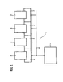
- FIG. 1 shows a bus system 1 with slots 2 for receiving modules 3.
- the slots 2 and thus also recorded in the slots 2 modules 3 are connected to each other via bus lines 4.
- a central processing unit 5 (CPU) is also connected to the bus lines 4.
- the entirety of the bus lines 4 is referred to as a bus.
- the central unit 5 can be accommodated in one of the slots or, as shown, connected to the bus in a different way.
- the central unit 5 communicates with the modules 3 via the bus.
- the modules 3 can communicate with one another via the bus.
- the slots 2 or modules 3 are connected in parallel to the bus lines 4, so that is not affected by a failure or the withdrawal of a module 3, the bus traffic between the remaining modules 3 and the central unit 5 via the bus lines 4.
- Each of the slots 2 is assigned a unique within the bus system 1 address, via which the in the Slots 2 recorded assemblies 3 are each responsive.
- the in the Slots 2 recorded assemblies 3 are each responsive.
- a memory can also be integrated on the module, in which the user can, for example, can write an address using a programmer.
- Another known from the prior art possibility of addressing modules or slots is to lead to each slot an additional line.
- the central unit can select a module with the respective line and inform the module which address it receives. After that, the central unit Send data packets, because the respective module knows its own address and can thus find out for itself which of the sent data packets are intended for them.
- the disadvantage of this solution is that an additional line must be routed to each slot. However, especially in a system with many slots, this means a significantly increased hardware cost.
- the central unit before starting the actual data traffic, the central unit must select each module by means of the additional line and in each case notify it of the address to which it is to react. If an assembly is taken out of such a bus system (eg because it is defective) and replaced by a new module, then the central unit must recognize that the module has been replaced and must in turn transmit the address to the new module.
- the central unit can push data through all modules.
- it first addresses all modules via parallel bus lines to inform them that they should switch to the shift register mode.
- the modules then together form a large shift register with, for example, 128-bit length (eg 16 modules with 8-bit shift registers each).
- the central unit pushes a data packet with exactly 128-bit length over an additional, through-ground line through the modules.
- the module addresses are arranged such that after sliding by 128 bits in each shift register within an assembly exactly the respective module address exists.
- the central unit can inform the modules about the parallel bus lines that they should read the shift register contents and use them as the module address.
- the modules own address is known.
- the central unit can then send data packets to the modules via the parallel bus lines.
- the disadvantage of this solution is in addition to the additional Direction that the modules must have integrated a shift register and must be strung together gapless. As soon as a slot is not occupied, the cross-section shift register is interrupted. The central unit then has no possibility to transmit the modules that are inserted after the gap to the address.
- an address is permanently set at each slot with pins. This requires additional connector pins. For 16 slots, e.g. 4 connector pins required to assign each slot a unique address.
- the bus system according to the invention avoids the disadvantages of the described solutions known from the prior art.
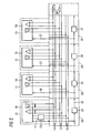
- FIG. 2 shows a bus system in which the slots via a bus line 14, a first signal with a first clock edge and an additional line 40, a second signal is transmitted with a second clock edge.
- the bus system according to FIG. 2 has so-called bus modules 29, which have slots for modules 10-13.
- the received in the first slot assembly 10 is in this case a central unit.
- the remaining three slots contain peripheral modules in this case.
- the connection between the individual slots is made with the bus modules 29.
- the bus is formed by bus lines 14-16.
- the bus lines 14 are designed as so-called write lines, the bus lines 15 as so-called read lines and the bus lines 16 as power supply lines.
- the bus lines 14, 15, also called data lines, are terminated at the physical bus end in each case by a terminating resistor 28.
- the power supply lines 16 are fed via a power supply 17 of the central unit 10.
- the assemblies 10 - 13 each have a user-specific integrated circuit, the so-called Bus ASIC 18, 19, which handles the communication of the modules 10
- the central unit feeds a first electrical signal with a first, instantaneous clock edge.
- the first signal or the first clock edge is therefore instantaneously at all slots.
- the central unit feeds a second electrical signal with a second, with respect to the first clock edge initially undelayed clock edge.
- the clock edge is delayed by time delay means 24 - 27 each for a certain time.
- the time delay means 24 - 27 in the bus module can be realized as active components (eg monoflop) or over propagation times with different line lengths.
- the number of slots that can be addressed in this way has no physical limit. This method can therefore also be used when a large number of modules are to be operated on a bus. If e.g. 100 modules are operated, it is still possible to recognize the slot safely.
- the time difference is then 100 ms in the above example. A very accurate time measurement is very easy to implement in the modules.
- an assembly 11-13 If an assembly 11-13 is plugged into the bus system, it measures the time difference between the clock edge of the respective signal 20-22 and the clock edge of the signal transmitted via the data line, ie the time difference between the occurrence of the signal change on the data line and the occurrence of the Signal change at the delay line. Based on the measured time difference, it recognizes the slot.
- the assignment between the value of the respective time difference and the respective address is known to the module or is carried out automatically by a suitable circuit arrangement for setting the address. The circuit thus allows the assemblies 11-13 to independently recognize their slot.
- the unambiguous assignment of an address to each slot and the unique assignment of the address to a time difference of the module accommodated at the respective slot thus enables an independent address setting.
- the module measures a time difference of 2 ms.
- the invention thus relates to a bus system 1 with slots 2 for receiving modules 3. It is proposed that for simple, automatic assignment of each address to a slot 2 via a data line of the bus system, a first signal with a first clock edge is transmitted and the slots 2 a tapped by a recorded on the respective slot 2 module 3 second signal can be supplied with a second clock edge, wherein from a time difference between the second and the first clock edge, an address of the respective slot 2 is uniquely determined.
- the invention also relates to an assembly 3, which is suitable for receiving at least one of the slots 2 of such a bus system 1, wherein the assembly 3 evaluation means for evaluating the time difference between the second and the first clock edge and for assigning an address depending on the result of Evaluation has.
Description
Die Erfindung betrifft ein Bussystem mit Steckplätzen zur Aufnahme von Baugruppen, wobei jedem Steckplatz eine Adresse zugeordnet ist, sowie eine Baugruppe, die zur Aufnahme an einem der Steckplätze eines solchen Bussystems geeignet ist.The invention relates to a bus system with slots for receiving modules, each slot is assigned an address, and an assembly that is suitable for receiving at one of the slots of such a bus system.
Ein solches Bussystem mit Steckplätzen zur Aufnahme von Baugruppen kann Teil einer speicherprogrammierbaren Steuerung in einem Automatisierungssystem, insbesondere einem industriellen Automatisierungssystem, sein. Ein solches Bussystem hat üblicherweise die Eigenschaft, dass Baugruppen herausgezogen werden können, ohne dass der Busverkehr zu den anderen Baugruppen des Bussystems unterbrochen wird. Um das zu erreichen, verwendet man eine Backplane mit Steckplätzen, in die alle Baugruppen hineingesteckt werden. Auf der Backplane verlaufen die Busleitungen, an welche die Baugruppen parallel angeschlossen werden. Von einem Teilnehmer am Busverkehr, z.B. einer Zentraleinheit (CPU = Central Processing Unit) können Daten über die Datenleitungen des Bus versendet werden. Solche Daten werden von allen an den Bus angeschlossenen Baugruppen empfangen.Such a bus system with slots for receiving modules may be part of a programmable logic controller in an automation system, in particular an industrial automation system. Such a bus system usually has the property that modules can be pulled out without the bus traffic is interrupted to the other modules of the bus system. To achieve this, you use a backplane with slots, in which all modules are inserted. On the backplane run the bus lines to which the modules are connected in parallel. From a subscriber to the bus, e.g. a central processing unit (CPU = Central Processing Unit) data can be sent over the data lines of the bus. Such data is received by all modules connected to the bus.
Sind die Daten nur für eine der empfangenen Baugruppen relevant, so muss diese Baugruppe einzeln adressierbar sein. Daher wird üblicherweise den einzelnen Steckplätzen jeweils eine im Bussystem eindeutige Adresse zugeordnet. Eine Baugruppe, welche an einem Steckplatz mit einer zugewiesenen Adresse angeschlossen ist, kann somit über diese Adresse adressiert werden. Ein von einem Teilnehmer gesendetes, für die jeweilige Baugruppe bestimmtes Datenpaket enthält somit neben den Nutzdaten auch eine Information über die Adresse des Steckplatzes bzw. der Baugruppe, welche von der jeweiligen Baugruppe erkannt wird. Einer Baugruppe auf einem bestimmten Steckplatz muss zuvor jedoch mitgeteilt werden, dass sie der Teilnehmer mit der jeweiligen Adresse ist, damit sie darauf reagieren kann, wenn Daten auf dem Bus versendet werden, in denen die jeweilige Empfängeradresse eingetragen ist.If the data is only relevant for one of the modules received, then this module must be individually addressable. Therefore, usually the individual slots each assigned a unique address in the bus system. An assembly which is connected to a slot with an assigned address can thus be addressed via this address. A data packet sent by a subscriber and intended for the respective module thus contains not only the user data but also information about the address of the slot or the module which is recognized by the respective module. However, an assembly on a particular slot must first be told that it has the Subscriber with the respective address is, so that she can react when data is sent on the bus, in which the respective recipient address is entered.
Für das Problem der Steckplatzerkennung bzw. Adresseinstellung gibt es verschiedene Lösungsmöglichkeiten. So sind manuelle Adressschalter auf der Baugruppe oder die Taufe der Baugruppe im Werk oder beim Kunden üblich. Weitere bekannte Lösungen verwenden eine Adressauswahlleitung auf dem Bus, eine durch die Baugruppen durchgeschliffene Busleitung oder Konfigurationspins auf dem Bus. Diese Lösungen weisen verschiedene Nachteile auf. So verlangen sie teilweise vom Anwender eine fehlerträchtige Aktion, verursachen erhöhte Softwareaufwendungen in der Zentraleinheit, benötigen zusätzliche Steckerpins oder verursachen generell zusätzliche Kosten.There are various possible solutions to the problem of slot recognition or address setting. Thus, manual address switches on the module or the christening of the module in the factory or at the customer are common. Other known solutions use an address selection line on the bus, a bus line ground through the modules, or configuration pins on the bus. These solutions have several disadvantages. Thus, they sometimes require a user-error-prone action, cause increased software expense in the central processing unit, require additional connector pins, or generally incur additional costs.
Nach
Der Erfindung liegt die Aufgabe zugrunde, eine vereinfachte Steckplatzerkennung zu ermöglichen.The invention has for its object to provide a simplified slot recognition.
Diese Aufgabe wird durch ein Bussystem gemäß Patentanspruch 1 sowie durch eine Baugruppe gemäß Patentanspruch 7 gelöst. Das erfindungsgemäße Bussystem weist Steckplätze zur Aufnahme von Baugruppen auf, wobei über eine Datenleitung des Bussystems ein erstes Signal mit einer ersten Taktflanke übermittelbar ist, wobei zur Zuordnung von jeweils einer Adresse zu einem Steckplatz den Steckplätzen ein durch eine an dem jeweiligen Steckplatz aufgenommene Baugruppe abgreifbares zweites Signal mit einer zweiten Taktflanke zuführbar ist, wobei aus einer Zeitdifferenz zwischen der zweiten und der ersten Taktflanke eine Adresse des jeweiligen Steckplatzes eindeutig ermittelbar ist und wobei durch jeden Steckplatz die Zeitdifferenz zwischen der zweiten und der ersten Taktflanke um eine vordefinierte und somit im System bekannte Zeit vergrößert wird.This object is achieved by a bus system according to claim 1 and by an assembly according to claim 7. The bus system according to the invention has slots for receiving modules, via a data line of the bus system, a first signal with a first clock edge is transmittable, wherein for assigning each address to a slot the slots a tapped by a recorded on the respective module assembly second Signal can be supplied with a second clock edge, wherein from a time difference between the second and the first clock edge, an address of the respective slot is uniquely determined and wherein each slot by the time difference between the second and the first clock edge by a predefined and thus known in the system time is enlarged.
Sie erfindungsgemäße Baugruppe ist zur Aufnahme an mindestens einem der Steckplätze eines solchen Bussystems geeignet, wobei die Baugruppe Auswertemittel zur Auswertung der Zeitdifferenz zwischen der zweiten und der ersten Taktflanke und zur Zuordnung einer Adresse in Abhängigkeit vom Ergebnis der Auswertung aufweist.The module according to the invention is suitable for receiving at least one of the slots of such a bus system, wherein the module has evaluation means for evaluating the time difference between the second and the first clock edge and for assigning an address in dependence on the result of the evaluation.
Die erfindungsgemäße Lösung ermöglicht es den Baugruppen, den Steckplatz bzw. die Adresse des Steckplatzes, an welchem sie aufgenommen werden, selbstständig zu erkennen.The solution according to the invention makes it possible for the modules to independently recognize the slot or the address of the slot on which they are received.
Die erfindungsgemäße Baugruppe weist vorteilhafterweise Auswertemittel zur Messung der Zeitdifferenz zwischen der zweiten und der ersten Taktflanke auf. Vorteilhafterweise werden die Auswertemittel als anwenderspezifisch integrierte Schaltung (ASIC) ausgeführt.The assembly according to the invention advantageously has evaluation means for measuring the time difference between the second and the first clock edge. Advantageously the evaluation means designed as a user-specific integrated circuit (ASIC).
Vorteilhafterweise wird ein solches Bussystem innerhalb einer speicherprogrammierbaren Steuerung bzw. eines Automatisierungssystems, insbesondere eines industriellen Automatisierungssystems, eingesetzt.Advantageously, such a bus system is used within a programmable logic controller or an automation system, in particular an industrial automation system.
Nachfolgend wird die Erfindung anhand der in den Figuren dargestellten Ausführungsbeispiele näher beschrieben und erläutert.The invention will be described and explained in more detail with reference to the exemplary embodiments illustrated in the figures.
Es zeigen:
- FIG 1
- ein Bussystem mit Steckplätzen zur Aufnahme von Baugruppen und
- FIG 2
- ein Bussystem, bei welchem den Steckplätzen ein erstes und ein zweites Signal zugeführt wird.
- FIG. 1
- a bus system with slots for accommodating modules and
- FIG. 2
- a bus system in which the slots a first and a second signal is supplied.
Zum einen ist üblich, über Adressschalter auf der Baugruppe oder eine Taufe der Baugruppe im Werk oder beim Kunden die Adresse einzustellen. Es ist möglich, auf der Baugruppe einen Adressschalter zu integrieren, mit welchem die Adresse manuell eingestellt werden kann. Die Baugruppe, z.B. eine digitale Ausgabebaugruppe, vergleicht die Adresse aus einem über den Bus versendeten Datenpaket mit der Adresse, die über den Schalter eingestellt ist. Stimmen beide Adressen überein, so erkennt die Baugruppe, dass das Datenpaket für sie bestimmt ist und kann darauf reagieren. Nachteilig an dieser Lösung ist insbesondere, dass ein Anwender die Adresse von Hand an jeder Baugruppe einstellen muss. Wird an zwei Baugruppen versehentlich die gleiche Adresse eingestellt, so funktioniert das gesamte Bussystem nicht mehr, weil eine Datenkollision auftritt. Ebenso führt es zu Fehlern, wenn bei der Baugruppe eine falsche Adresse eingestellt wird. Die Adresseinstellung von Hand ist somit fehlerträchtig und umständlich, da der Anwender bei einem Baugruppenwechsel die Adresse an der neuen Baugruppe von Hand einstellen muss und die neue Baugruppe nicht einfach in das Bussystem bzw. den Steckplatz hineinstecken kann. Statt des Adressschalters kann auch ein Speicher auf der Baugruppe integriert sein, in welchen der Anwender z.B. mittels eines Programmiergeräts eine Adresse hineinschreiben kann.On the one hand, it is customary to set the address via address switches on the module or a christening of the module at the factory or at the customer's site. It is possible to integrate an address switch on the module with which the address can be set manually. The assembly, e.g. a digital output module, compares the address from a data packet sent over the bus with the address set via the switch. If both addresses match, the module recognizes that the data packet is intended for them and can react to them. A particular disadvantage of this solution is that a user must set the address manually on each module. If the same address is accidentally set on two modules, the entire bus system will no longer work because of a data collision. It also leads to errors if an incorrect address is set for the module. The address setting by hand is thus error-prone and cumbersome because the user must set the address on the new module by hand when changing a module and the new module can not simply plug into the bus system or the slot. Instead of the address switch, a memory can also be integrated on the module, in which the user can, for example, can write an address using a programmer.
Eine weitere aus dem Stand der Technik bekannte Möglichkeit der Adressierung von Baugruppen bzw. Steckplätzen besteht darin, zu jedem Steckplatz eine zusätzliche Leitung zu führen. In diesem Fall kann die Zentraleinheit einer Baugruppe mit der jeweiligen Leitung anwählen und der Baugruppe mitteilen, welche Adresse sie bekommt. Danach kann die Zentraleinheit Datenpakete verschicken, weil die jeweilige Baugruppe ihre eigene Adresse kennt und damit selbst herausfinden kann, welche der versendeten Datenpakete für sie bestimmt sind. Nachteilig an dieser Lösung ist es, dass eine zusätzliche Leitung zu jedem Steckplatz geführt werden muss. Insbesondere bei einem System mit vielen Steckplätzen bedeutet das jedoch einen wesentlich erhöhten Hardwareaufwand. Zudem muss die Zentraleinheit vor Beginn des eigentlichen Datenverkehrs jede Baugruppe mittels der zusätzlichen Leitung selektieren und ihr jeweils die Adresse mitteilen, auf welche sie reagieren soll. Wird eine Baugruppe aus einem solchen Bussystem herausgenommen (z.B. weil sie defekt ist) und gegen eine neue Baugruppe ausgetauscht, so muss die Zentraleinheit erkennen, dass die Baugruppe gewechselt wurde und muss der neuen Baugruppe wiederum die Adresse übermitteln.Another known from the prior art possibility of addressing modules or slots is to lead to each slot an additional line. In this case, the central unit can select a module with the respective line and inform the module which address it receives. After that, the central unit Send data packets, because the respective module knows its own address and can thus find out for itself which of the sent data packets are intended for them. The disadvantage of this solution is that an additional line must be routed to each slot. However, especially in a system with many slots, this means a significantly increased hardware cost. In addition, before starting the actual data traffic, the central unit must select each module by means of the additional line and in each case notify it of the address to which it is to react. If an assembly is taken out of such a bus system (eg because it is defective) and replaced by a new module, then the central unit must recognize that the module has been replaced and must in turn transmit the address to the new module.
Eine weitere aus dem Stand der Technik bekannte Möglichkeit besteht darin, ein serielles Schieberegister zu verwenden. Die Zentraleinheit kann in diesem Fall Daten durch alle Baugruppen hindurch schieben. Dabei spricht sie zuerst alle Baugruppen über parallele Busleitungen an um ihnen mitzuteilen, dass sie in den Schieberegistermodus umschalten sollen. Die Baugruppen bilden dann zusammen ein großes Schieberegister mit z.B. 128 Bit Länge (z.B. 16 Baugruppen mit je 8 Bit Schieberegister). In diesem Fall schiebt die Zentraleinheit ein Datenpaket mit genau 128 Bit Länge über eine zusätzliche, durchgeschliffene Leitung durch die Baugruppen hindurch. In diesem Datenpaket sind die Baugruppenadressen derart angeordnet, dass nach dem Schieben um 128 Bit in jedem Schieberegister innerhalb einer Baugruppe genau die jeweilige Baugruppenadresse vorliegt. In einem nächsten Schritt kann die Zentraleinheit über die parallelen Busleitungen den Baugruppen mitteilen, dass sie den Schieberegisterinhalt auslesen und als Baugruppenadresse verwenden sollen. Damit ist den Baugruppen die eigene Adresse bekannt. Die Zentraleinheit kann daraufhin Datenpakete über die parallelen Busleitungen an die Baugruppen senden. Nachteilig an dieser Lösung ist neben der zusätzlichen Leitung, dass die Baugruppen ein Schieberegister integriert haben müssen sowie lückenlos aneinandergereiht sein müssen. Sobald ein Steckplatz nicht belegt ist, wird das baugruppenübergreifende Schieberegister unterbrochen. Die Zentraleinheit hat dann keine Möglichkeit, den Baugruppen, die nach der Lücke gesteckt sind, die Adresse zu übermitteln.Another possibility known from the prior art is to use a serial shift register. In this case, the central unit can push data through all modules. In the process, it first addresses all modules via parallel bus lines to inform them that they should switch to the shift register mode. The modules then together form a large shift register with, for example, 128-bit length (
Bei einer weiteren aus dem Stand der Technik bekannten Lösung wird an jedem Steckplatz mit Pins eine Adresse fest eingestellt. Dafür werden zusätzliche Steckerpins benötigt. Bei 16 Steckplätzen sind z.B. 4 Steckerpins nötig, um jedem Steckplatz eine eindeutige Adresse zuzuordnen.In another solution known from the prior art, an address is permanently set at each slot with pins. This requires additional connector pins. For 16 slots, e.g. 4 connector pins required to assign each slot a unique address.
Das erfindungsgemäße Bussystem vermeidet die Nachteile der beschriebenen aus dem Stand der Technik bekannten Lösungen.The bus system according to the invention avoids the disadvantages of the described solutions known from the prior art.
In eine der Datenleitungen, in die Busleitung 14, speist die Zentraleinheit ein erstes elektrisches Signal mit einer ersten, unverzögerten Taktflanke ein. Das erste Signal bzw. die erste Taktflanke steht somit an allen Steckplätzen unverzögert an. In die zusätzliche Leitung 40 speist die Zentraleinheit ein zweites elektrisches Signal mit einer zweiten, gegenüber der ersten Taktflanke vorerst unverzögerten Taktflanke ein. Auf der Backplane bzw. in den Busmodulen 29 wird die Taktflanke durch Zeitverzögerungsmittel 24 - 27 jeweils um eine bestimmte Zeit verzögert. Die Zeitverzögerungsmittel 24 - 27 im Busmodul können als aktive Bauteile (z. B. Monoflop) oder über Laufzeiten mit unterschiedlichen Leitungslängen realisiert werden. Gemäß dem Ausführungsbeispiel wird die Taktflanke an jedem Steckplatz bzw. in jedem Busmodul 29 um die konstante Verzögerungszeit T = 1 ms verzögert. Die Baugruppen 11 - 13 greifen das zweite Signal 20 - 22 mit der zweiten Taktflanke am jeweiligen Steckplatz ab. Anhand der jeweiligen Zeitdifferenz zwischen der zweiten Taktflanke des zweiten Signals auf der Leitung 40, auch Verzögerungsleitung genannt, und der ersten Taktflanke des ersten Signals auf der Datenleitung erkennen die Baugruppen 11 - 13, auf welchem Steckplatz sie sich befinden. Beispielsweise speist die Zentraleinheit 10 am ersten Steckplatz zum Zeitpunkt t = 0 je ein Signal mit einer Taktflanke (im Folgenden Signalwechsel genannt) auf die Datenleitung und die Verzögerungsleitung ein. Der Signalwechsel an der Datenleitung steht unverzögert zum Zeitpunkt t = 0 an allen Steckplätzen an.
Der Signalwechsel an der Verzögerungsleitung steht zum Zeitpunkt t = 1 * T (z. B. = 1 ms) am zweiten Steckplatz an.
Der Signalwechsel an der Verzögerungsleitung steht zum Zeitpunkt t = 2 * T (z. B. = 2 ms) am dritten Steckplatz an.
Der Signalwechsel an der Verzögerungsleitung steht zum Zeitpunkt t = 3 * T (z. B. = 3 ms) am vierten Steckplatz an.In one of the data lines, in the
The signal change on the delay line arrives at the second slot at time t = 1 * T (eg = 1 ms).
The signal change on the delay line arrives at the third slot at time t = 2 * T (eg = 2 ms).
The signal change on the delay line arrives at the fourth slot at time t = 3 * T (eg = 3 ms).
Entsprechend würde der Signalwechsel jeweils um die Zeitdifferenz T = 1 ms verzögert an weiteren Steckplätzen anstehen, wenn diese vorhanden wären. Der Anzahl der solchermaßen adressierbaren Steckplätze ist keine physikalische Grenze gesetzt. Dieses Verfahren kann daher auch dann angewendet werden, wenn sehr viele Baugruppen an einem Bus betrieben werden sollen. Wenn z.B. 100 Baugruppen betrieben werden, ist es trotzdem noch möglich, den Steckplatz sicher zu erkennen. Die Zeitdifferenz beträgt im oben genannten Beispiel dann 100 ms. Eine sehr genaue Zeitmessung ist in den Baugruppen sehr einfach zu realisieren.Correspondingly, the signal change would each be delayed by the time difference T = 1 ms at further slots, if they were present. The number of slots that can be addressed in this way has no physical limit. This method can therefore also be used when a large number of modules are to be operated on a bus. If e.g. 100 modules are operated, it is still possible to recognize the slot safely. The time difference is then 100 ms in the above example. A very accurate time measurement is very easy to implement in the modules.
Wird eine Baugruppe 11 - 13 in das Bussystem gesteckt, so misst sie die Zeitdifferenz zwischen der Taktflanke des jeweiligen Signals 20 - 22 und der Taktflanke des über die Datenleitung übermittelten Signals, d. h. die Zeitdifferenz zwischen dem Auftreten des Signalwechsels an der Datenleitung und dem Auftreten des Signalwechsels an der Verzögerungsleitung. Anhand der jeweils gemessenen Zeitdifferenz erkennt sie den Steckplatz. Die Zuordnung zwischen dem Wert der jeweiligen Zeitdifferenz und der jeweiligen Adresse ist der Baugruppe bekannt oder erfolgt durch eine geeignete Schaltungsanordnung zur Einstellung der Adresse automatisch. Die Schaltung ermöglicht es den Baugruppen 11 - 13 somit, ihren Steckplatz selbstständig zu erkennen. Durch die eindeutige Zuordnung einer Adresse zu jedem Steckplatz und durch die eindeutige Zuordnung der Adresse zu einer Zeitdifferenz ist der am jeweiligen Steckplatz aufgenommenen Baugruppe somit eine selbstständige Adresseinstellung ermöglicht. Beispiel: Die Baugruppe misst eine Zeitdifferenz von 2 ms. Sie steckt also auf dem dritten Steckplatz. Wenn die Zentraleinheit nun ein Datenpaket für den dritten Steckplatz sendet, erkennt die Baugruppe, dass es für sie bestimmt ist. Im Unterschied zum Stand der Technik muss somit weder eine manuelle Adresseinstellung erfolgen, noch müssen in der Zentraleinheit Softwaremechanismen zur Adressübertragung in die Baugruppe 11 - 13 ablaufen. Lediglich eine zusätzliche Leitung 40 innerhalb des Bussystems ist notwendig. Die Eigenstromaufnahme der vorgeschlagenen Schaltungsanordnung ist sehr gering und die Schaltung ist kostengünstig herzustellen. Zudem sind Zeitdifferenzen mit relativ einfachen Mitteln sehr genau zu bestimmen.If an assembly 11-13 is plugged into the bus system, it measures the time difference between the clock edge of the respective signal 20-22 and the clock edge of the signal transmitted via the data line, ie the time difference between the occurrence of the signal change on the data line and the occurrence of the Signal change at the delay line. Based on the measured time difference, it recognizes the slot. The assignment between the value of the respective time difference and the respective address is known to the module or is carried out automatically by a suitable circuit arrangement for setting the address. The circuit thus allows the assemblies 11-13 to independently recognize their slot. The unambiguous assignment of an address to each slot and the unique assignment of the address to a time difference of the module accommodated at the respective slot thus enables an independent address setting. Example: The module measures a time difference of 2 ms. So she is in the third slot. When the central unit sends a data packet for the third slot, the module detects that it is intended for it. In contrast to the prior art, therefore, neither a manual address setting must be carried out, nor do software mechanisms for address transmission in the module 11 - 13 have to run in the central unit. Only one
Zusammengefasst betrifft die Erfindung somit ein Bussystem 1 mit Steckplätzen 2 zur Aufnahme von Baugruppen 3. Es wird vorgeschlagen, dass zur einfachen, automatischen Zuordnung von jeweils einer Adresse zu einem Steckplatz 2 über eine Datenleitung des Bussystems ein erstes Signal mit einer ersten Taktflanke übermittelbar ist und den Steckplätzen 2 ein durch eine an dem jeweiligen Steckplatz 2 aufgenommene Baugruppe 3 abgreifbares zweites Signal mit einer zweiten Taktflanke zuführbar ist, wobei aus einer Zeitdifferenz zwischen der zweiten und der ersten Taktflanke eine Adresse des jeweiligen Steckplatzes 2 eindeutig ermittelbar ist. Die Erfindung betrifft zudem eine Baugruppe 3, die zur Aufnahme an mindestens einem der Steckplätze 2 eines solchen Bussystems 1 geeignet ist, wobei die Baugruppe 3 Auswertemittel zur Auswertung der Zeitdifferenz zwischen der zweiten und der ersten Taktflanke und zur Zuordnung einer Adresse in Abhängigkeit vom Ergebnis der Auswertung aufweist.In summary, the invention thus relates to a bus system 1 with
Claims (11)
- Bus system (1) with plug-in locations (2) for accommodating modules (3), whereby a first signal with a first clock edge can be conveyed by way of a data line of the bus system, whereby in each case in order to assign an address to a plug-in location (2) a second signal with a second clock edge which can be read off by means of a module (3) accommodated at the plug-in location (2) in question can be delivered to the plug-in locations (2), whereby an address for the plug-in location (2) in question can be determined uniquely from a time difference between the second and the first clock edge.
characterised in that
the time difference between the second and the first clock edge is increased through each plug-in location by a predefined time which is thus known in the system. - Bus system according to claim 1,
characterised in that
the plug-in locations (2) are connected in parallel to bus lines (4). - Bus system according to claim 1 or 2,
characterised in that
the second signal can be delivered by way of an additional line (40) to the plug-in locations (2). - Bus system according to one of the preceding claims,
characterised in that
the second signal can be delivered in such a manner that the time difference between the second and the first clock edge is different at each plug-in location (2). - Bus system according to one of the preceding claims,
characterised in that
the time difference between the second and the first clock edge at each plug-in location (2) is increased by a predefined time with reference to the time difference between the second and the first clock edge at a preceding plug-in location (2). - Bus system according to one of the preceding claims,
characterised in that
the second signal is forwarded to a following plug-in location after being delayed by a predefined time by a preceding plug-in location. - Module (3), which is suitable for inclusion in at least one of the plug-in locations (2) of a bus system (1) according to one of the preceding claims, whereby the module (3) has evaluation facilities for evaluating the time difference between the second and the first clock edge and for making an address assignment depending on the result of the evaluation.
- Module according to claim 7,
characterised in that
the evaluation facilities are provided for measuring the time difference between the second and the first clock edge. - Module according to claim 7 or 8,
characterised in that
the evaluation facilities are implemented as an application-specific integrated circuit. - Programmable logic controller with a bus system according to one of claims 1 to 6.
- Automation system, particularly an industrial automation system, with a programmable logic controller according to claim 10.
Priority Applications (2)
| Application Number | Priority Date | Filing Date | Title |
|---|---|---|---|
| DE200450007058 DE502004007058D1 (en) | 2004-06-30 | 2004-06-30 | Slot recognition in a bus system |
| EP20040015410 EP1612681B1 (en) | 2004-06-30 | 2004-06-30 | Slot recognition for a bus system |
Applications Claiming Priority (1)
| Application Number | Priority Date | Filing Date | Title |
|---|---|---|---|
| EP20040015410 EP1612681B1 (en) | 2004-06-30 | 2004-06-30 | Slot recognition for a bus system |
Publications (2)
| Publication Number | Publication Date |
|---|---|
| EP1612681A1 EP1612681A1 (en) | 2006-01-04 |
| EP1612681B1 true EP1612681B1 (en) | 2008-05-07 |
Family
ID=34925558
Family Applications (1)
| Application Number | Title | Priority Date | Filing Date |
|---|---|---|---|
| EP20040015410 Expired - Fee Related EP1612681B1 (en) | 2004-06-30 | 2004-06-30 | Slot recognition for a bus system |
Country Status (2)
| Country | Link |
|---|---|
| EP (1) | EP1612681B1 (en) |
| DE (1) | DE502004007058D1 (en) |
Family Cites Families (3)
| Publication number | Priority date | Publication date | Assignee | Title |
|---|---|---|---|---|
| DE3303826A1 (en) * | 1983-02-04 | 1984-08-09 | Siemens AG, 1000 Berlin und 8000 München | Memory-programmable controller |
| US5179670A (en) * | 1989-12-01 | 1993-01-12 | Mips Computer Systems, Inc. | Slot determination mechanism using pulse counting |
| AU3437193A (en) * | 1993-01-06 | 1994-08-15 | 3Do Company, The | Expansion bus |
-
2004
- 2004-06-30 EP EP20040015410 patent/EP1612681B1/en not_active Expired - Fee Related
- 2004-06-30 DE DE200450007058 patent/DE502004007058D1/en active Active
Also Published As
| Publication number | Publication date |
|---|---|
| EP1612681A1 (en) | 2006-01-04 |
| DE502004007058D1 (en) | 2008-06-19 |
Similar Documents
| Publication | Publication Date | Title |
|---|---|---|
| DE3300260C2 (en) | ||
| DE3300261C2 (en) | ||
| EP3131016A1 (en) | Dynamic addressing | |
| DE3300263A1 (en) | CIRCUIT ARRANGEMENT FOR ALLOCATING ACCESS TO A REQUIRED COLLECTION LINE | |
| DE3111555C2 (en) | Method and apparatus for storing information using prior recording | |
| DE19532639C2 (en) | Device for single-channel transmission of data originating from two data sources | |
| DE102004046618A1 (en) | Circuit arrangement for analog / digital conversion | |
| DE4416879B4 (en) | Control device with means for switching between two data lines | |
| DE4026581C2 (en) | ||
| EP3047635B1 (en) | Field bus coupler for connecting modules to a field bus and method for addressing such modules | |
| DE102004037227A1 (en) | Method and device for addressing subscribers of a bus system | |
| EP1612681B1 (en) | Slot recognition for a bus system | |
| DE4344904A1 (en) | Connection of activators and sensors to field bus | |
| EP1612689B1 (en) | Identification of slots in a bus system | |
| DE19645057C2 (en) | Device for the selection of address words by means of demultiplex decoding | |
| DE19645054C2 (en) | Device and method for selecting address words | |
| DE4122276C2 (en) | Hierarchical synchronization process for a digital communication system | |
| DE102017113538B4 (en) | Control device for a power semiconductor switch | |
| DE2527236C3 (en) | Arrangement for inserting data in a register | |
| DE3325791C2 (en) | Circuit arrangement for peripheral units cooperating with a central control device | |
| EP0762246B1 (en) | Method and device for checking a control unit | |
| DE10111468B4 (en) | Method and device for determining properties of inserted modules | |
| DE19645055C2 (en) | Electrical circuit arrangement for serial evaluation of a bit sequence | |
| DE3202543C2 (en) | Circuit arrangement for checking the correspondence of two binary words | |
| EP0788043A2 (en) | Method and fieldbus system for serial data transmission in object oriented applications |
Legal Events
| Date | Code | Title | Description |
|---|---|---|---|
| PUAI | Public reference made under article 153(3) epc to a published international application that has entered the european phase |
Free format text: ORIGINAL CODE: 0009012 |
|
| AK | Designated contracting states |
Kind code of ref document: A1 Designated state(s): AT BE BG CH CY CZ DE DK EE ES FI FR GB GR HU IE IT LI LU MC NL PL PT RO SE SI SK TR |
|
| AX | Request for extension of the european patent |
Extension state: AL HR LT LV MK |
|
| 17P | Request for examination filed |
Effective date: 20060206 |
|
| AKX | Designation fees paid |
Designated state(s): DE FR GB IT |
|
| GRAP | Despatch of communication of intention to grant a patent |
Free format text: ORIGINAL CODE: EPIDOSNIGR1 |
|
| GRAS | Grant fee paid |
Free format text: ORIGINAL CODE: EPIDOSNIGR3 |
|
| GRAA | (expected) grant |
Free format text: ORIGINAL CODE: 0009210 |
|
| AK | Designated contracting states |
Kind code of ref document: B1 Designated state(s): DE FR GB IT |
|
| REG | Reference to a national code |
Ref country code: GB Ref legal event code: FG4D Free format text: NOT ENGLISH |
|
| REF | Corresponds to: |
Ref document number: 502004007058 Country of ref document: DE Date of ref document: 20080619 Kind code of ref document: P |
|
| PLBE | No opposition filed within time limit |
Free format text: ORIGINAL CODE: 0009261 |
|
| STAA | Information on the status of an ep patent application or granted ep patent |
Free format text: STATUS: NO OPPOSITION FILED WITHIN TIME LIMIT |
|
| 26N | No opposition filed |
Effective date: 20090210 |
|
| PGFP | Annual fee paid to national office [announced via postgrant information from national office to epo] |
Ref country code: IT Payment date: 20120626 Year of fee payment: 9 |
|
| PG25 | Lapsed in a contracting state [announced via postgrant information from national office to epo] |
Ref country code: IT Free format text: LAPSE BECAUSE OF NON-PAYMENT OF DUE FEES Effective date: 20130630 |
|
| PGFP | Annual fee paid to national office [announced via postgrant information from national office to epo] |
Ref country code: GB Payment date: 20150608 Year of fee payment: 12 |
|
| REG | Reference to a national code |
Ref country code: FR Ref legal event code: PLFP Year of fee payment: 13 |
|
| PGFP | Annual fee paid to national office [announced via postgrant information from national office to epo] |
Ref country code: FR Payment date: 20160615 Year of fee payment: 13 |
|
| PGFP | Annual fee paid to national office [announced via postgrant information from national office to epo] |
Ref country code: DE Payment date: 20160819 Year of fee payment: 13 |
|
| GBPC | Gb: european patent ceased through non-payment of renewal fee |
Effective date: 20160630 |
|
| PG25 | Lapsed in a contracting state [announced via postgrant information from national office to epo] |
Ref country code: GB Free format text: LAPSE BECAUSE OF NON-PAYMENT OF DUE FEES Effective date: 20160630 |
|
| REG | Reference to a national code |
Ref country code: DE Ref legal event code: R119 Ref document number: 502004007058 Country of ref document: DE |
|
| REG | Reference to a national code |
Ref country code: FR Ref legal event code: ST Effective date: 20180228 |
|
| PG25 | Lapsed in a contracting state [announced via postgrant information from national office to epo] |
Ref country code: DE Free format text: LAPSE BECAUSE OF NON-PAYMENT OF DUE FEES Effective date: 20180103 |
|
| PG25 | Lapsed in a contracting state [announced via postgrant information from national office to epo] |
Ref country code: FR Free format text: LAPSE BECAUSE OF NON-PAYMENT OF DUE FEES Effective date: 20170630 |