EP1611552B1 - Coin acceptor - Google Patents
Coin acceptor Download PDFInfo
- Publication number
- EP1611552B1 EP1611552B1 EP04725412A EP04725412A EP1611552B1 EP 1611552 B1 EP1611552 B1 EP 1611552B1 EP 04725412 A EP04725412 A EP 04725412A EP 04725412 A EP04725412 A EP 04725412A EP 1611552 B1 EP1611552 B1 EP 1611552B1
- Authority
- EP
- European Patent Office
- Prior art keywords
- coin
- path
- guiding surface
- acceptor according
- coil
- Prior art date
- Legal status (The legal status is an assumption and is not a legal conclusion. Google has not performed a legal analysis and makes no representation as to the accuracy of the status listed.)
- Expired - Lifetime
Links
Images


Classifications
-
- G—PHYSICS
- G07—CHECKING-DEVICES
- G07D—HANDLING OF COINS OR VALUABLE PAPERS, e.g. TESTING, SORTING BY DENOMINATIONS, COUNTING, DISPENSING, CHANGING OR DEPOSITING
- G07D5/00—Testing specially adapted to determine the identity or genuineness of coins, e.g. for segregating coins which are unacceptable or alien to a currency
- G07D5/08—Testing the magnetic or electric properties
-
- G—PHYSICS
- G07—CHECKING-DEVICES
- G07F—COIN-FREED OR LIKE APPARATUS
- G07F1/00—Coin inlet arrangements; Coins specially adapted to operate coin-freed mechanisms
- G07F1/04—Coin chutes
- G07F1/046—Coin chutes with means for dealing with jamming, e.g. by bent wires
Definitions
- This invention relates to an improved acceptor for coins, tokens or like items with an attributable monetary value.
- Conventional coin acceptors include a coin rundown path down which coins travel through a sensing station where sensors detect characteristics of the coin. Examples are described in our GB-A-2 169 429 and WO99/23615 . Also, reference is directed to EP-A-0 704 825 and US-B-6 173 8261 .
- inductive sensors are provided at the sensing station which perform inductive coin tests and produce coin parameter signals that are a function of the material and metallic content of the coin under test. Other sensors may be used, such as one or more optical sensors.
- the coin parameter signals are digitised and compared with stored coin data by means of a micro controller to determine the acceptability and often the denomination of the tested coin. If the coin is found to be acceptable, the micro controller operates an accept gate and the coin is directed to an accept path, but otherwise the accept gate remains closed and the coin is directed to a reject path.
- the coin rundown path comprises an inclined rundown surface or flight deck, along which the coins roll edgewise through the coin sensing station, the flight deck being disposed between closely spaced, generally upwardly extending side walls which maintain the coin with its perimeter edge on the flight deck.
- One or both of the side walls may be inclined to the vertical so to encourage the coin under test to tip over whilst moving down the flight path, so that one of its major surfaces tends to slide along one of the side walls. This is intended to reduce wobbling of the coin on the rundown path.
- Coin wobble can vary the distance between the inductive sensors and successive coins as they pass through the sensing station, and produce an unwanted variation in the inductive coupling with the sensors from coin to coin as they are tested, which degrades the coin parameter signals.
- Coins may become jammed in the coin rundown path.
- this problem has been addressed by moving the side walls apart to clear the jam.
- One of the sidewalls is formed as a part of the main body of the acceptor and the other side wall is defined by a surface on a door that is hinged on the main body.
- a release mechanism is operated to open the hinged door slightly, thereby moving apart the side walls so that the jammed coin can fall off the flight deck and into the reject path.
- the provision of a door however, undesirably adds to the manufacturing cost of the coin acceptor.
- a flexible wiring harness needs to be provided to accommodate the hinge and connect the sensors to the micro controller on the main body. The harness also adds to the manufacturing cost.
- a coin acceptor comprising a coin sensing station, a coin rundown path extending through the sensing station, the path including a coin guiding surface on which a major face of the coin lies in sliding engagement during its passage along the path through the sensing station, wherein the path is curved such that the said face of the coin is urged by centripetal force against the coin guiding surface as it moves along the path and through the sensing station.
- the pressing of the major surface of the coin against the coin guiding surface by centripetal force reduces the likelihood of coin wobble. Also, the coin path can be made much wider than hitherto, which may obviate the need for a coin jam release mechanism such as the hinged door often used hitherto.
- the coin acceptor may have a main body with the coin guiding surface, and a cover mounted on the body, such that the coin path extends between said surface and the cover.
- the cover can fixedly mounted on the body, without the need for a coin jam release mechanism.
- a coin inlet may be provided, with a curved inlet surface for guiding a coin inserted in the inlet to a particular region of the coin guiding surface.
- the coin acceptor may comprise sensor coils at the coin sensing station, one of said coils comprising an elongate winding extending longitudinally along the coin rundown path.
- the elongate coil may be wound on an elongate former which is longer than it is wide and may be longer than the maximum diameter of coins to be accepted thereby.
- Processing circuitry may be coupled to the elongate coil to derive therefrom a coin parameter signal as a function of coin diameter.
- At least one coil of circular cross section may also be provided at the sensing station, which has a diameter smaller than the minimum diameter of coins to be accepted.
- the coin acceptor may have a side wall opposite to the coin guiding surface, said coin rundown path extending between the coin guiding surface and the sidewall, wherein said side wall is fixedly mounted relative to the curved coin guiding surface.
- the acceptor may include pressure relief holes through the coin guiding surface.
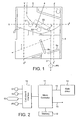
- FIG. 1 illustrates the general configuration of a multi-denomination acceptor according to the invention.
- the acceptor includes a main body 1 with a coin run-down path 2 along which coins under test pass edgewise from an inlet 3 through a coin sensing station 4 and then fall towards a gate 5 which has first and second gate arms 5a, 5b that open and close a coin accept path 6 and a coin reject path 7.
- a test is performed on each coin as it passes through the sensing station 4. If the outcome of the test indicates the presence of a true coin, the gate arm 5a is opened and arm 5b is closed so that the coin can pass to the accept path 6, but otherwise, the gate arm 5a remains closed and the gate arm 5b closed so that the coin is deflected to the reject path 7.
- the coin path through the acceptor for a coin 8 is shown schematically by dotted line 9.
- the coin sensing station 4 includes three coin sensing coil units S1, S2 and S3, which are energised in order to produce an inductive coupling with the coin. Also, a coil unit PS is provided in the accept path 6, downstream of the gate 5, to act as a credit sensor in order to detect whether a coin that was determined to be acceptable, has in fact passed into the accept path 6.
- the credit sensor may be mounted in a cash box (not shown) that receives true coins from the accept path rather than the acceptor itself.
- the coils are energised at different frequencies by a drive and interface circuit 10 shown schematically in Figure 2 .
- Eddy currents are induced in the coin under test by the coil units.
- the different inductive couplings between the four coils and the coin characterise the coin substantially uniquely.
- the drive and interface circuit 10 produces corresponding digital coin parameter data signals x 1 , x 2 , x 3 as a function of the different inductive couplings between the coin and the coil units S1, S2, S3 and S4.
- a corresponding signal is produced for the coil unit PS.
- the coils S1 and S2 have a small diameter in relation to the diameter of coins under test in order to detect the inductive characteristics of individual chordal regions of the coin.
- Coil unit S3 is wound on an elongate bobbin and extends along the coin path. The configuration of the coil units will be explained in more detail hereinafter.
- the coin parameter signals produced by a coin under test are fed to a microcontroller 11 which is coupled to a memory 12.
- the microcontroller 11 processes the coin parameter signals x 1 , - x 3 derived from the coin under test and compares the outcome with corresponding stored values held in the memory 12.
- the stored values are held in terms of windows having upper and lower value limits. Thus, if the processed data falls within the corresponding windows associated with a true coin of a particular denomination, the coin is indicated to be acceptable, but otherwise is rejected. If acceptable, a signal is provided on line 13 to a drive circuit 14 which operates the gate 5 shown in Figure 1 so as to allow the coin to pass to the accept path 6. Otherwise, the gate 5 is not opened and the coin passes to reject path 7.
- the microcontroller 11 compares the processed data with a number of different sets of operating window data appropriate for coins of different denominations so that the coin acceptor can accept or reject more than one coin of a particular currency set. If the coin is accepted, its passage along the accept path 6 is detected by the post acceptance credit sensor coil unit PS, and the unit 10 passes corresponding data to the microcontroller 11, which in turn provides an output on line 15 that indicates the amount of monetary credit attributed to the accepted coin.
- the sensor coil units S each include an inductor coil connected in an individual oscillatory circuit and the coil drive and interface circuit 10 includes a multiplexer to scan outputs from the coil units sequentially, so as to provide data to the microcontroller 11.
- Each circuit typically oscillates at a frequency in a range of 50-150 kHz and the circuit components are selected so that each sensor coil S1-S4 has a different natural resonant frequency in order to avoid cross-coupling between them.
- each of the sensor coil unit S1-S3 its impedance is altered by the presence of the coin over a period of ⁇ 100 milliseconds.
- the amplitude of the oscillations through the coil is modified over the period that the coin passes and also the oscillation frequency is altered.
- the variation in amplitude and frequency resulting from the modulation produced by the coin is used to produce the coin parameter signals x 1 , - x 3 representative of characteristics of the coin.
- Figure 3 is a schematic, perspective, exploded view of the coin acceptor, showing the main body 1 together with left and right covers 16, 17.
- the path 9 for coins is defined between the main body 1 and the right cover 16.
- the electronics shown in Figure 2 are mounted (out of view in Figure 3 ) on the main body and is covered by the left cover 17. Both of the covers 16, 17 are fixedly located on the main body 1 in use. There is no conventional door arrangement to allow the release of coin jams.
- the acceptor has a front side surface 18, rear side surface 19, top surface 20, and underside 21.
- the coin rundown path 2 is defined by a curved surface 22 on the main body 1 and a curved coin guiding surface 23 on the right side cover 16.
- the coin guiding surface 23 extends into the coin inlet 3 as can be seen from the top plan view of Figure 5 .
- the curvature of the coin guiding surface 23 decreases towards the front side surface 18 so as to guide incoming coins towards the front side wall 18 as they enter the acceptor through the coin inlet 3. This will be explained later.
- the right side cover also includes an inclined, coin rundown edge 24 to guide coins along the rundown path 2.
- the coin guiding surface 22 is curved both when viewed in horizontal and vertical section and extends from the coin inlet 3 to a generally vertical planar surface region 25 on the main body 1, illustrated in Figure 3 .
- the surface 22 has a radius of curvature R h in a horizontal direction and also a curvature R v in horizontal section.
- R h radius of curvature
- R v curvature
- Figures 11 and 12 illustrate the passage of a coin 26 through the coin sensing station 4.
- the curved surface 23 on the right side cover 16 guides the coin onto the curved surface 22 on the main body 1 and also directs it towards the front side wall 18 into the position shown in Figure 12 .
- the coin thus travels in the direction of arrow A from the inlet 3 to the position shown in Figure 12 .
- the coin 26 moves in a curved path shown by arrow B through the coin sensing station.
- the coin falls by gravity down the inclined ledge 24 and the generally vertically and horizontally curved nature of the surface 22 ensures that one of the major circular side faces of the coin 26 is slidably engaged with surface 22 and is urged by a centripetal force against the surface 22 as it moves along path B through the sensing station 4.
- tendency for the coin to wobble is materially reduced due to the fact that it is held by centripetal force in sliding engagement with the surface 22.
- conventional validators have used a linear path so that even if the coin were inclined to the vertical, the rotating coin would tend to try and stand upright as a result of its rotation thereby inducing coin wobble.
- the coin 26 is urged against surface 22 by centripetal force, spacing between the side walls of the coin rundown path can be made larger than in conventional coin acceptors, obviating the requirement for a hinged door to release coin jams.
- the right side cover 16 can be fixedly attached to the main body 1 without the need for a hinged coin door to clear coin jams.
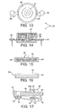
- FIG. 13 and 14 illustrate the construction of the sensor coils S1 and S2.
- Each of the coils comprises a generally cylindrical bobbin 27 of plastics material, on which windings of a coil 28 are formed.
- Bobbin 27 is push fitted into a so-called half pot core 29 made of sintered ferrite material.
- the ends of the winding 28 are mounted in plastics terminal pieces 30 that extend through slots 31 in the cylindrical side wall of the half pot core 29.
- FIGs 15 and 16 are plan and side views respectively of the sensor coil S3.
- the coil comprises an elongate bobbin 32 made of ferrite material on which copper windings 33 are formed.
- the bobbin is mounted on a rectangular mounting bracket 34 that has a locating lug 35.
- the coils S1, S2 and S3 are push fitted into a mounting bracket 36 is provided with recesses 37, 38 and 39 to receive the coils S1, S2 and S3 respectively, with the recess 39 including a region 39a to receive the locating lug 35 on coil S3.
- the mounting bracket 36 is held by screws fitted through mounting holes 40, 41 on the rear of the inclined surface 22 as illustrated in Figure 6 .
- FIGs 18 and 19 illustrate the response produced by the sensor coils S1, S2 and S3 as coin 26 on the curved surface 22.
- the coin 26 is shown moving from position 26-1 to 26-2.
- the amplitude deviation of the signal x 1 is a function primarily of the material of which the coin is made and the coil senses the material content of the coin along the cordal region of the coin.
- a similar output is produced by coil S2. Since coil S2 is energised in a different frequency from coil S1 the amplitude deviation is different but similarly dependent on the material from which the coin is made.
- the elongate coil S3 provides an indication of the diameter of the coin. As the coin passes the coil, a generally rectangular amplitude deviation x 3 is produced as shown in Figure 19 and it will be understood that the width d of the pulse, from time t1 to t2, is dependent on coin diameter. It has been found in accordance with the invention that the elongate coil S3 provides a highly reliable indication of coin diameter.
- coils S1-S3 are all mounted on the same side of the coin rundown path, on the rear wall of the main body that provides the curved surface 22.
- the inductive coupling with a coin under test can reliably be formed with the coils through the curved surface 22, and the coin is urged against it by centripetal force, as previously explained. Therefore the distance between the coin under test and the coils S1-S3 remains substantially constant from coin to coin, which improves reliability of the coin parameter signals produced by the coils.
- providing the coils S1-S3 only one side of the path 2 has the advantage that no electrical connections need to be made between the main body 1 and the right cover 16, which reduces the cost of the coin acceptor.
- the curved surface 22 includes negative pressure relief holes 43. It has been found that as the coin 26 slides over the surface 22, the intimate contact between the coins and the surface can give rise to a negative pressure region being developed between the surface of a coin that contacts the curved surface 22, which can impede progress of the coin along the path.
- the negative pressure relief holes 43 cause any negative pressure to be released and thereby free up the progress of the coin along the rundown path.
- the acceptor Whilst the acceptor has been described for use with coins, it can also be used with tokens and other similar items with an attributable monetary value. Also, the retaining force for the coin as it moves over the curved surface may comprise a centrifugal force and the term centripetal as used herein is to be interpreted accordingly.
Landscapes
- Physics & Mathematics (AREA)
- General Physics & Mathematics (AREA)
- Testing Of Coins (AREA)
- Organic Low-Molecular-Weight Compounds And Preparation Thereof (AREA)
- Polyoxymethylene Polymers And Polymers With Carbon-To-Carbon Bonds (AREA)
- Luminescent Compositions (AREA)
- Optical Fibers, Optical Fiber Cores, And Optical Fiber Bundles (AREA)
Abstract
Description
- This invention relates to an improved acceptor for coins, tokens or like items with an attributable monetary value.
- Conventional coin acceptors include a coin rundown path down which coins travel through a sensing station where sensors detect characteristics of the coin. Examples are described in our
GB-A-2 169 429 WO99/23615 EP-A-0 704 825 andUS-B-6 173 8261 - The coin rundown path comprises an inclined rundown surface or flight deck, along which the coins roll edgewise through the coin sensing station, the flight deck being disposed between closely spaced, generally upwardly extending side walls which maintain the coin with its perimeter edge on the flight deck. One or both of the side walls may be inclined to the vertical so to encourage the coin under test to tip over whilst moving down the flight path, so that one of its major surfaces tends to slide along one of the side walls. This is intended to reduce wobbling of the coin on the rundown path. Coin wobble can vary the distance between the inductive sensors and successive coins as they pass through the sensing station, and produce an unwanted variation in the inductive coupling with the sensors from coin to coin as they are tested, which degrades the coin parameter signals.
- Coins may become jammed in the coin rundown path. Conventionally, this problem has been addressed by moving the side walls apart to clear the jam. One of the sidewalls is formed as a part of the main body of the acceptor and the other side wall is defined by a surface on a door that is hinged on the main body. In the event of a coin jam, a release mechanism is operated to open the hinged door slightly, thereby moving apart the side walls so that the jammed coin can fall off the flight deck and into the reject path. The provision of a door however, undesirably adds to the manufacturing cost of the coin acceptor. Also, if the sensors are mounted on the door, a flexible wiring harness needs to be provided to accommodate the hinge and connect the sensors to the micro controller on the main body. The harness also adds to the manufacturing cost.
- In accordance with invention there is provided a coin acceptor comprising a coin sensing station, a coin rundown path extending through the sensing station, the path including a coin guiding surface on which a major face of the coin lies in sliding engagement during its passage along the path through the sensing station, wherein the path is curved such that the said face of the coin is urged by centripetal force against the coin guiding surface as it moves along the path and through the sensing station.
- The pressing of the major surface of the coin against the coin guiding surface by centripetal force reduces the likelihood of coin wobble. Also, the coin path can be made much wider than hitherto, which may obviate the need for a coin jam release mechanism such as the hinged door often used hitherto.
- The coin acceptor may have a main body with the coin guiding surface, and a cover mounted on the body, such that the coin path extends between said surface and the cover. The cover can fixedly mounted on the body, without the need for a coin jam release mechanism.
- A coin inlet may be provided, with a curved inlet surface for guiding a coin inserted in the inlet to a particular region of the coin guiding surface.
- The coin acceptor may comprise sensor coils at the coin sensing station, one of said coils comprising an elongate winding extending longitudinally along the coin rundown path.
- The elongate coil may be wound on an elongate former which is longer than it is wide and may be longer than the maximum diameter of coins to be accepted thereby. Processing circuitry may be coupled to the elongate coil to derive therefrom a coin parameter signal as a function of coin diameter.
- At least one coil of circular cross section may also be provided at the sensing station, which has a diameter smaller than the minimum diameter of coins to be accepted.
- The coin acceptor may have a side wall opposite to the coin guiding surface, said coin rundown path extending between the coin guiding surface and the sidewall, wherein said side wall is fixedly mounted relative to the curved coin guiding surface.
- The acceptor may include pressure relief holes through the coin guiding surface.
- In order that the invention may be more fully understood an embodiment thereof will now be described by way of example with reference to the accompanying drawings in which:
-
Figure 1 is a schematic block diagram of a coin acceptor in accordance with the invention; -
Figure 2 is a schematic block diagram of the circuits of the acceptor shown inFigure 1 ; -
Figure 3 is schematic, perspective, exploded view of the acceptor; -
Figure 4 is a side view of the interior surface of the right side cover; -
Figure 5 is a top plan view of the acceptor; -
Figure 6 is a horizontal sectional view of the acceptor taken along the line X-X' inFigure 1 , with the right side cover shown detached from the body and the left side cover omitted; -
Figure 7 is a vertical sectional view of the acceptor taken along the line Y-Y' inFigure 1 , with the right side cover shown detached from the body and the left side cover omitted; -
Figure 8 is a vertical sectional view of the acceptor taken along the line Z-Z' inFigure 1 , with the right side cover shown detached from the body and the left side cover omitted; -
Figure 9 illustrates the horizontal curvature of the coin guiding surface through the coin sensing station; -
Figure 10 illustrates the vertical curvature of the coin guiding surface through the coin sensing station; -
Figure 11 is a top plan view of the acceptor when a coin enters its coin inlet; -
Figure 12 is a schematic illustration of the passage of the coin through the coin sensing station; -
Figure 13 is a plan view of one of the sensor coils S1, S2; -
Figure 14 is a sectional view of the coil shown inFigure 13 ; -
Figure 15 is a top plan view of the sensor coil S3; -
Figure 16 is a side view of the coil shown inFigure 15 ; -
Figure 17 is a plan view of a mounting for the sensor coils; -
Figure 18 is a schematic illustration of the interaction between the coin and the sensor coils; -
Figure 19 is an illustration of the waveforms produced by the interaction ofFigure 18 ; and -
Figure 20 is a schematic sectional view corresponding toFigure 10 , of a modified coin guiding surface -
Figure 1 illustrates the general configuration of a multi-denomination acceptor according to the invention. The acceptor includes amain body 1 with a coin run-downpath 2 along which coins under test pass edgewise from aninlet 3 through acoin sensing station 4 and then fall towards a gate 5 which has first andsecond gate arms path 6 and acoin reject path 7. A test is performed on each coin as it passes through thesensing station 4. If the outcome of the test indicates the presence of a true coin, thegate arm 5a is opened andarm 5b is closed so that the coin can pass to theaccept path 6, but otherwise, thegate arm 5a remains closed and thegate arm 5b closed so that the coin is deflected to thereject path 7. The coin path through the acceptor for a coin 8 is shown schematically by dotted line 9. - The
coin sensing station 4 includes three coin sensing coil units S1, S2 and S3, which are energised in order to produce an inductive coupling with the coin. Also, a coil unit PS is provided in theaccept path 6, downstream of the gate 5, to act as a credit sensor in order to detect whether a coin that was determined to be acceptable, has in fact passed into theaccept path 6. The credit sensor may be mounted in a cash box (not shown) that receives true coins from the accept path rather than the acceptor itself. - The coils are energised at different frequencies by a drive and
interface circuit 10 shown schematically inFigure 2 . Eddy currents are induced in the coin under test by the coil units. The different inductive couplings between the four coils and the coin characterise the coin substantially uniquely. The drive andinterface circuit 10 produces corresponding digital coin parameter data signals x1, x2, x3 as a function of the different inductive couplings between the coin and the coil units S1, S2, S3 and S4. A corresponding signal is produced for the coil unit PS. The coils S1 and S2 have a small diameter in relation to the diameter of coins under test in order to detect the inductive characteristics of individual chordal regions of the coin. Improved discrimination can be achieved by making the area A of the coil unit S which faces the coin, for the coil units S1 and S2, smaller than 72 mm2, which permits the inductive characteristics of individual regions of the coin's face to be sensed. Coil unit S3 is wound on an elongate bobbin and extends along the coin path. The configuration of the coil units will be explained in more detail hereinafter. - In order to determine coin authenticity, the coin parameter signals produced by a coin under test are fed to a
microcontroller 11 which is coupled to amemory 12. Themicrocontroller 11 processes the coin parameter signals x1, - x3 derived from the coin under test and compares the outcome with corresponding stored values held in thememory 12. The stored values are held in terms of windows having upper and lower value limits. Thus, if the processed data falls within the corresponding windows associated with a true coin of a particular denomination, the coin is indicated to be acceptable, but otherwise is rejected. If acceptable, a signal is provided online 13 to adrive circuit 14 which operates the gate 5 shown inFigure 1 so as to allow the coin to pass to the acceptpath 6.
Otherwise, the gate 5 is not opened and the coin passes to rejectpath 7. - The
microcontroller 11 compares the processed data with a number of different sets of operating window data appropriate for coins of different denominations so that the coin acceptor can accept or reject more than one coin of a particular currency set. If the coin is accepted, its passage along the acceptpath 6 is detected by the post acceptance credit sensor coil unit PS, and theunit 10 passes corresponding data to themicrocontroller 11, which in turn provides an output online 15 that indicates the amount of monetary credit attributed to the accepted coin. - The sensor coil units S each include an inductor coil connected in an individual oscillatory circuit and the coil drive and
interface circuit 10 includes a multiplexer to scan outputs from the coil units sequentially, so as to provide data to themicrocontroller 11. Each circuit typically oscillates at a frequency in a range of 50-150 kHz and the circuit components are selected so that each sensor coil S1-S4 has a different natural resonant frequency in order to avoid cross-coupling between them. - As the coin passes each of the sensor coil unit S1-S3, its impedance is altered by the presence of the coin over a period of ∼100 milliseconds. As a result, the amplitude of the oscillations through the coil is modified over the period that the coin passes and also the oscillation frequency is altered. The variation in amplitude and frequency resulting from the modulation produced by the coin is used to produce the coin parameter signals x1, - x3 representative of characteristics of the coin.
-
Figure 3 is a schematic, perspective, exploded view of the coin acceptor, showing themain body 1 together with left and right covers 16, 17. The path 9 for coins is defined between themain body 1 and theright cover 16. The electronics shown inFigure 2 are mounted (out of view inFigure 3 ) on the main body and is covered by theleft cover 17. Both of thecovers main body 1 in use. There is no conventional door arrangement to allow the release of coin jams. The acceptor has afront side surface 18,rear side surface 19,top surface 20, andunderside 21. - The
coin rundown path 2 is defined by acurved surface 22 on themain body 1 and a curvedcoin guiding surface 23 on theright side cover 16. Thecoin guiding surface 23 extends into thecoin inlet 3 as can be seen from the top plan view ofFigure 5 . The curvature of thecoin guiding surface 23 decreases towards thefront side surface 18 so as to guide incoming coins towards thefront side wall 18 as they enter the acceptor through thecoin inlet 3. This will be explained later. - Referring to
Figures 3 and 4 , the right side cover also includes an inclined, coinrundown edge 24 to guide coins along therundown path 2. - As shown in the sectional view of
Figures 6 - 8 , thecoin guiding surface 22 is curved both when viewed in horizontal and vertical section and extends from thecoin inlet 3 to a generally verticalplanar surface region 25 on themain body 1, illustrated inFigure 3 . - As shown in
Figures 9 and 10 , thesurface 22 has a radius of curvature Rh in a horizontal direction and also a curvature Rv in horizontal section. Thus, as the coin moves across thesurface 22 as it travels along the path 9, it moves both in a horizontal and vertical curve. -
Figures 11 and 12 illustrate the passage of acoin 26 through thecoin sensing station 4. As shown inFigure 11 , whencoin 26 is inserted into thecoin inlet 3, thecurved surface 23 on theright side cover 16, guides the coin onto thecurved surface 22 on themain body 1 and also directs it towards thefront side wall 18 into the position shown inFigure 12 . The coin thus travels in the direction of arrow A from theinlet 3 to the position shown inFigure 12 . - Thereafter, the
coin 26 moves in a curved path shown by arrow B through the coin sensing station. The coin falls by gravity down theinclined ledge 24 and the generally vertically and horizontally curved nature of thesurface 22 ensures that one of the major circular side faces of thecoin 26 is slidably engaged withsurface 22 and is urged by a centripetal force against thesurface 22 as it moves along path B through thesensing station 4. Thus, tendency for the coin to wobble is materially reduced due to the fact that it is held by centripetal force in sliding engagement with thesurface 22. In contrast, conventional validators have used a linear path so that even if the coin were inclined to the vertical, the rotating coin would tend to try and stand upright as a result of its rotation thereby inducing coin wobble. - When the coin reaches the end of path B, it then falls due to gravity along path C over the generally
vertical surface 25 to be accepted or rejected on acceptpath 6 or rejectpath 7 in the manner previously described, under the control of gate 5. - Since the
coin 26 is urged againstsurface 22 by centripetal force, spacing between the side walls of the coin rundown path can be made larger than in conventional coin acceptors, obviating the requirement for a hinged door to release coin jams. Thus, theright side cover 16 can be fixedly attached to themain body 1 without the need for a hinged coin door to clear coin jams. - The configuration of the sensor coils S1, S2 and S3 will now be described in more detail.
Figures 13 and 14 illustrate the construction of the sensor coils S1 and S2. Each of the coils comprises a generallycylindrical bobbin 27 of plastics material, on which windings of acoil 28 are formed.Bobbin 27 is push fitted into a so-calledhalf pot core 29 made of sintered ferrite material. The ends of the winding 28 are mounted in plasticsterminal pieces 30 that extend throughslots 31 in the cylindrical side wall of thehalf pot core 29. -
Figures 15 and 16 are plan and side views respectively of the sensor coil S3. The coil comprises anelongate bobbin 32 made of ferrite material on whichcopper windings 33 are formed. The bobbin is mounted on a rectangular mountingbracket 34 that has a locatinglug 35. The coils S1, S2 and S3 are push fitted into a mountingbracket 36 is provided withrecesses recess 39 including aregion 39a to receive the locatinglug 35 on coil S3. The mountingbracket 36 is held by screws fitted through mountingholes inclined surface 22 as illustrated inFigure 6 . -
Figures 18 and 19 illustrate the response produced by the sensor coils S1, S2 and S3 ascoin 26 on thecurved surface 22. InFigure 18 , thecoin 26 is shown moving from position 26-1 to 26-2. As thecoin 26 moves past coil S2, it forms a inductive coupling with the coil and a corresponding coin parameter signal x1 produced by the coil S1 is shown inFigure 19 as a function of time. The amplitude deviation of the signal x1 is a function primarily of the material of which the coin is made and the coil senses the material content of the coin along the cordal region of the coin. A similar output is produced by coil S2. Since coil S2 is energised in a different frequency from coil S1 the amplitude deviation is different but similarly dependent on the material from which the coin is made. - The elongate coil S3 provides an indication of the diameter of the coin. As the coin passes the coil, a generally rectangular amplitude deviation x3 is produced as shown in
Figure 19 and it will be understood that the width d of the pulse, from time t1 to t2, is dependent on coin diameter. It has been found in accordance with the invention that the elongate coil S3 provides a highly reliable indication of coin diameter. - An advantage of the arrangement of coils S1-S3 is that they are all mounted on the same side of the coin rundown path, on the rear wall of the main body that provides the
curved surface 22. Thus, the inductive coupling with a coin under test can reliably be formed with the coils through thecurved surface 22, and the coin is urged against it by centripetal force, as previously explained. Therefore the distance between the coin under test and the coils S1-S3 remains substantially constant from coin to coin, which improves reliability of the coin parameter signals produced by the coils. - Also, providing the coils S1-S3 only one side of the
path 2 has the advantage that no electrical connections need to be made between themain body 1 and theright cover 16, which reduces the cost of the coin acceptor. - Referring now to
Figure 20 , a modification of the acceptor is shown, in which thecurved surface 22 includes negative pressure relief holes 43. It has been found that as thecoin 26 slides over thesurface 22, the intimate contact between the coins and the surface can give rise to a negative pressure region being developed between the surface of a coin that contacts thecurved surface 22, which can impede progress of the coin along the path. In accordance with the invention, the negative pressure relief holes 43 cause any negative pressure to be released and thereby free up the progress of the coin along the rundown path. - Whilst the acceptor has been described for use with coins, it can also be used with tokens and other similar items with an attributable monetary value. Also, the retaining force for the coin as it moves over the curved surface may comprise a centrifugal force and the term centripetal as used herein is to be interpreted accordingly.
Claims (13)
- A coin acceptor comprising a coin sensing station (4), a coin run-down path (2) extending through the sensing station, the path including a coin guiding surface (22) on which a major face of the coin lies in sliding engagement during its passage along the path through the sensing station, characterised in that the path is curved such that the said face of the coin is urged by centripetal force against the coin guiding surface as it moves along the path and through the sensing station.
- A coin acceptor according to claim 1 comprising a body (1) including the coin guiding surface, and a cover (16) mounted on the body, wherein the coin path extends between said surface and the cover.
- A coin acceptor according to claim 2 wherein the cover (16) is fixedly mounted on the body, without a coin jam release mechanism.
- A coin acceptor according to any preceding claim including a coin inlet opening (3) and a curved inlet surface (23) for guiding a coin inserted in the inlet to a particular region of the coin guiding surface.
- A coin acceptor according to any preceding claim including wherein the coin guiding surface (22) is configured to relieve a pressure differential between the major face of the coin and the coin guiding surface.
- A coin acceptor according to claim 5 including pressure relief holes (43) through the coin guiding surface.
- A coin acceptor according to any preceding claim including sensor coils (S1, S2, S3) at the coin sensing station (4), one of said coils (S3) comprising an elongate winding extending longitudinally along the coin rundown path.
- A coin acceptor according to claim 7 wherein the elongate coil is wound on an elongate former (32) which is longer than it is wide.
- A coin acceptor according to claim 8 wherein the elongate coil is longer than the maximum diameter of coins to be accepted thereby.
- A coin acceptor according to claim 7, 8 or 9 including at least one coil (S1, S2) of circular cross section at the sensing station.
- A coin acceptor according to claim 10 wherein the circular coil has a diameter smaller than the minimum diameter of coins to be accepted thereby.
- A coin acceptor according to any one of claims 7 to 11 including processing circuitry (10, 11) coupled to the elongate coil to derive therefrom a coin parameter signal as a function of coin diameter.
- A coin acceptor according to claim 1 including a side wall (16) opposite to the coin guiding surface, said coin rundown path (2) extending between the coin guiding surface (22) and the sidewall, wherein said side wall is fixedly mounted relative to the curved coin guiding surface.
Applications Claiming Priority (2)
| Application Number | Priority Date | Filing Date | Title |
|---|---|---|---|
| GB0307880A GB2400223A (en) | 2003-04-04 | 2003-04-04 | Guiding coins in a coin acceptor |
| PCT/GB2004/001457 WO2004088597A1 (en) | 2003-04-04 | 2004-04-02 | Coin acceptor |
Publications (2)
| Publication Number | Publication Date |
|---|---|
| EP1611552A1 EP1611552A1 (en) | 2006-01-04 |
| EP1611552B1 true EP1611552B1 (en) | 2008-10-08 |
Family
ID=9956239
Family Applications (1)
| Application Number | Title | Priority Date | Filing Date |
|---|---|---|---|
| EP04725412A Expired - Lifetime EP1611552B1 (en) | 2003-04-04 | 2004-04-02 | Coin acceptor |
Country Status (8)
| Country | Link |
|---|---|
| US (1) | US7617922B2 (en) |
| EP (1) | EP1611552B1 (en) |
| CN (1) | CN1802672A (en) |
| AT (1) | ATE410757T1 (en) |
| DE (1) | DE602004016977D1 (en) |
| ES (1) | ES2315653T3 (en) |
| GB (1) | GB2400223A (en) |
| WO (1) | WO2004088597A1 (en) |
Families Citing this family (4)
| Publication number | Priority date | Publication date | Assignee | Title |
|---|---|---|---|---|
| US7166845B1 (en) * | 2004-01-09 | 2007-01-23 | Crystal Photonics, Incorporated | Method of enhancing performance of cerium doped lutetium yttrium orthosilicate crystals and crystals produced thereby |
| JP5882772B2 (en) * | 2012-02-10 | 2016-03-09 | グローリー株式会社 | Magnetic sensor for coin identification |
| JP6992445B2 (en) * | 2017-11-27 | 2022-01-13 | 富士電機株式会社 | Coin detection antenna and coin processing device |
| CN113240851A (en) * | 2021-03-24 | 2021-08-10 | 浙江工业大学 | Coin recognition device and method suitable for coin exchange paper money equipment |
Family Cites Families (17)
| Publication number | Priority date | Publication date | Assignee | Title |
|---|---|---|---|---|
| BE795650A (en) * | 1972-02-23 | 1973-06-18 | Mars Inc | COINS SELECTION AND SORTING DEVICE |
| GB1468663A (en) * | 1973-05-18 | 1977-03-30 | Mars Inc | Coin handling apparatus with means for retarding the closing of a hinged cover |
| US4062435A (en) * | 1976-03-03 | 1977-12-13 | K-Jack Engineering Company, Inc. | Water proof coin mechanism |
| US4410077A (en) * | 1981-06-01 | 1983-10-18 | Umc Industries, Inc. | Coin handling apparatus with coin retardation feature |
| GB8500220D0 (en) * | 1985-01-04 | 1985-02-13 | Coin Controls | Discriminating between metallic articles |
| JPH0445100Y2 (en) * | 1985-07-16 | 1992-10-23 | ||
| FR2617311B1 (en) * | 1987-06-26 | 1991-05-31 | Crouzet Sa | DEVICE FOR INSERTING CURRENCY INTO PREPAYMENT APPARATUS |
| JPH0636205B2 (en) * | 1988-11-15 | 1994-05-11 | 旭精工株式会社 | Coin sorter |
| US5429550A (en) * | 1990-05-14 | 1995-07-04 | Cummins-Allison Corp. | Coin handling system with controlled coin discharge |
| ATE160639T1 (en) * | 1994-09-21 | 1997-12-15 | Landis & Gyr Tech Innovat | DEVICE FOR CHECKING THE AUTHENTICITY OF COINS, TOKENS OR OTHER FLAT METALLIC OBJECTS |
| GB2323199B (en) * | 1997-02-24 | 2000-12-20 | Mars Inc | Method and apparatus for validating coins |
| GB9723223D0 (en) * | 1997-11-03 | 1998-01-07 | Coin Controls | Coin validator |
| US6109417A (en) * | 1998-11-03 | 2000-08-29 | Parkway Machine Corporation | Anti-corruption coin/token input chute |
| US6206167B1 (en) * | 1999-09-27 | 2001-03-27 | Elcotel, Inc. | Coin turning coin-entrance chute |
| CA2293767C (en) * | 1999-12-24 | 2004-06-22 | Cashcode Company Inc. | Eddy-current sensor for coin evaluation |
| GB2359176B (en) * | 2000-02-09 | 2002-08-28 | Tetrel Ltd | Coin validation arrangement |
| DE60137063D1 (en) * | 2001-12-28 | 2009-01-29 | Mei Inc | Method and device for sorting currency articles |
-
2003
- 2003-04-04 GB GB0307880A patent/GB2400223A/en not_active Withdrawn
-
2004
- 2004-04-02 DE DE602004016977T patent/DE602004016977D1/en not_active Expired - Lifetime
- 2004-04-02 WO PCT/GB2004/001457 patent/WO2004088597A1/en not_active Ceased
- 2004-04-02 EP EP04725412A patent/EP1611552B1/en not_active Expired - Lifetime
- 2004-04-02 CN CNA200480008690XA patent/CN1802672A/en active Pending
- 2004-04-02 ES ES04725412T patent/ES2315653T3/en not_active Expired - Lifetime
- 2004-04-02 US US10/551,511 patent/US7617922B2/en not_active Expired - Fee Related
- 2004-04-02 AT AT04725412T patent/ATE410757T1/en not_active IP Right Cessation
Also Published As
| Publication number | Publication date |
|---|---|
| US7617922B2 (en) | 2009-11-17 |
| DE602004016977D1 (en) | 2008-11-20 |
| EP1611552A1 (en) | 2006-01-04 |
| ES2315653T3 (en) | 2009-04-01 |
| WO2004088597A1 (en) | 2004-10-14 |
| GB2400223A (en) | 2004-10-06 |
| US20070039800A1 (en) | 2007-02-22 |
| ATE410757T1 (en) | 2008-10-15 |
| GB0307880D0 (en) | 2003-05-14 |
| CN1802672A (en) | 2006-07-12 |
Similar Documents
| Publication | Publication Date | Title |
|---|---|---|
| US5379875A (en) | Coin discriminator and acceptor arrangement | |
| US6227343B1 (en) | Dual coil coin identifier | |
| EP0737345B1 (en) | Coin discriminator | |
| US5379876A (en) | Coin discrimination apparatus | |
| EP0369736A2 (en) | Method of discriminating coins | |
| EP2091027B1 (en) | Value medium processing apparatus | |
| EP1611552B1 (en) | Coin acceptor | |
| EP1151419B1 (en) | Money item acceptor | |
| EP0904580B1 (en) | Coin validator calibration | |
| EP0246993A2 (en) | A coin handling apparatus | |
| EP1029308A1 (en) | Coin acceptor | |
| JP2014044682A (en) | Paper sheet fatigue determination device, paper money processor and paper sheet fatigue determination method | |
| EP1581914B1 (en) | Money item acceptor with enhanced security | |
| JPH0585074B2 (en) | ||
| JP4955519B2 (en) | Coin deposit / withdrawal device | |
| KR101848006B1 (en) | Coin recognition apparatus for recycle type account module | |
| JPH06309543A (en) | Coin sorter | |
| JPH0455996A (en) | Coin sorter | |
| KR20060132132A (en) | Banknote identification device | |
| CA2139703A1 (en) | Coin discriminator and acceptor arrangement | |
| CN87100649A (en) | The device of voucher and reason voucher | |
| JP2012009083A (en) | Coin paying-in device |
Legal Events
| Date | Code | Title | Description |
|---|---|---|---|
| PUAI | Public reference made under article 153(3) epc to a published international application that has entered the european phase |
Free format text: ORIGINAL CODE: 0009012 |
|
| 17P | Request for examination filed |
Effective date: 20050928 |
|
| AK | Designated contracting states |
Kind code of ref document: A1 Designated state(s): AT BE BG CH CY CZ DE DK EE ES FI FR GB GR HU IE IT LI LU MC NL PL PT RO SE SI SK TR |
|
| AX | Request for extension of the european patent |
Extension state: AL HR LT LV MK |
|
| DAX | Request for extension of the european patent (deleted) | ||
| 17Q | First examination report despatched |
Effective date: 20060825 |
|
| GRAP | Despatch of communication of intention to grant a patent |
Free format text: ORIGINAL CODE: EPIDOSNIGR1 |
|
| GRAS | Grant fee paid |
Free format text: ORIGINAL CODE: EPIDOSNIGR3 |
|
| GRAA | (expected) grant |
Free format text: ORIGINAL CODE: 0009210 |
|
| AK | Designated contracting states |
Kind code of ref document: B1 Designated state(s): AT BE BG CH CY CZ DE DK EE ES FI FR GB GR HU IE IT LI LU MC NL PL PT RO SE SI SK TR |
|
| REG | Reference to a national code |
Ref country code: GB Ref legal event code: FG4D |
|
| REG | Reference to a national code |
Ref country code: CH Ref legal event code: EP |
|
| REG | Reference to a national code |
Ref country code: IE Ref legal event code: FG4D |
|
| REF | Corresponds to: |
Ref document number: 602004016977 Country of ref document: DE Date of ref document: 20081120 Kind code of ref document: P |
|
| PG25 | Lapsed in a contracting state [announced via postgrant information from national office to epo] |
Ref country code: SI Free format text: LAPSE BECAUSE OF FAILURE TO SUBMIT A TRANSLATION OF THE DESCRIPTION OR TO PAY THE FEE WITHIN THE PRESCRIBED TIME-LIMIT Effective date: 20081008 |
|
| NLV1 | Nl: lapsed or annulled due to failure to fulfill the requirements of art. 29p and 29m of the patents act | ||
| REG | Reference to a national code |
Ref country code: ES Ref legal event code: FG2A Ref document number: 2315653 Country of ref document: ES Kind code of ref document: T3 |
|
| PG25 | Lapsed in a contracting state [announced via postgrant information from national office to epo] |
Ref country code: AT Free format text: LAPSE BECAUSE OF FAILURE TO SUBMIT A TRANSLATION OF THE DESCRIPTION OR TO PAY THE FEE WITHIN THE PRESCRIBED TIME-LIMIT Effective date: 20081008 Ref country code: BG Free format text: LAPSE BECAUSE OF FAILURE TO SUBMIT A TRANSLATION OF THE DESCRIPTION OR TO PAY THE FEE WITHIN THE PRESCRIBED TIME-LIMIT Effective date: 20090108 |
|
| PG25 | Lapsed in a contracting state [announced via postgrant information from national office to epo] |
Ref country code: PL Free format text: LAPSE BECAUSE OF FAILURE TO SUBMIT A TRANSLATION OF THE DESCRIPTION OR TO PAY THE FEE WITHIN THE PRESCRIBED TIME-LIMIT Effective date: 20081008 Ref country code: FI Free format text: LAPSE BECAUSE OF FAILURE TO SUBMIT A TRANSLATION OF THE DESCRIPTION OR TO PAY THE FEE WITHIN THE PRESCRIBED TIME-LIMIT Effective date: 20081008 Ref country code: PT Free format text: LAPSE BECAUSE OF FAILURE TO SUBMIT A TRANSLATION OF THE DESCRIPTION OR TO PAY THE FEE WITHIN THE PRESCRIBED TIME-LIMIT Effective date: 20090218 Ref country code: NL Free format text: LAPSE BECAUSE OF FAILURE TO SUBMIT A TRANSLATION OF THE DESCRIPTION OR TO PAY THE FEE WITHIN THE PRESCRIBED TIME-LIMIT Effective date: 20081008 |
|
| PG25 | Lapsed in a contracting state [announced via postgrant information from national office to epo] |
Ref country code: BE Free format text: LAPSE BECAUSE OF FAILURE TO SUBMIT A TRANSLATION OF THE DESCRIPTION OR TO PAY THE FEE WITHIN THE PRESCRIBED TIME-LIMIT Effective date: 20081008 Ref country code: DK Free format text: LAPSE BECAUSE OF FAILURE TO SUBMIT A TRANSLATION OF THE DESCRIPTION OR TO PAY THE FEE WITHIN THE PRESCRIBED TIME-LIMIT Effective date: 20081008 Ref country code: RO Free format text: LAPSE BECAUSE OF FAILURE TO SUBMIT A TRANSLATION OF THE DESCRIPTION OR TO PAY THE FEE WITHIN THE PRESCRIBED TIME-LIMIT Effective date: 20081008 Ref country code: EE Free format text: LAPSE BECAUSE OF FAILURE TO SUBMIT A TRANSLATION OF THE DESCRIPTION OR TO PAY THE FEE WITHIN THE PRESCRIBED TIME-LIMIT Effective date: 20081008 |
|
| PLBE | No opposition filed within time limit |
Free format text: ORIGINAL CODE: 0009261 |
|
| STAA | Information on the status of an ep patent application or granted ep patent |
Free format text: STATUS: NO OPPOSITION FILED WITHIN TIME LIMIT |
|
| PG25 | Lapsed in a contracting state [announced via postgrant information from national office to epo] |
Ref country code: SE Free format text: LAPSE BECAUSE OF FAILURE TO SUBMIT A TRANSLATION OF THE DESCRIPTION OR TO PAY THE FEE WITHIN THE PRESCRIBED TIME-LIMIT Effective date: 20090108 Ref country code: CZ Free format text: LAPSE BECAUSE OF FAILURE TO SUBMIT A TRANSLATION OF THE DESCRIPTION OR TO PAY THE FEE WITHIN THE PRESCRIBED TIME-LIMIT Effective date: 20081008 |
|
| 26N | No opposition filed |
Effective date: 20090709 |
|
| PG25 | Lapsed in a contracting state [announced via postgrant information from national office to epo] |
Ref country code: SK Free format text: LAPSE BECAUSE OF FAILURE TO SUBMIT A TRANSLATION OF THE DESCRIPTION OR TO PAY THE FEE WITHIN THE PRESCRIBED TIME-LIMIT Effective date: 20081008 |
|
| REG | Reference to a national code |
Ref country code: CH Ref legal event code: PL |
|
| GBPC | Gb: european patent ceased through non-payment of renewal fee |
Effective date: 20090402 |
|
| REG | Reference to a national code |
Ref country code: FR Ref legal event code: ST Effective date: 20091231 |
|
| PG25 | Lapsed in a contracting state [announced via postgrant information from national office to epo] |
Ref country code: LI Free format text: LAPSE BECAUSE OF NON-PAYMENT OF DUE FEES Effective date: 20090430 Ref country code: CH Free format text: LAPSE BECAUSE OF NON-PAYMENT OF DUE FEES Effective date: 20090430 |
|
| REG | Reference to a national code |
Ref country code: IE Ref legal event code: MM4A |
|
| PG25 | Lapsed in a contracting state [announced via postgrant information from national office to epo] |
Ref country code: MC Free format text: LAPSE BECAUSE OF NON-PAYMENT OF DUE FEES Effective date: 20090430 Ref country code: GB Free format text: LAPSE BECAUSE OF NON-PAYMENT OF DUE FEES Effective date: 20090402 Ref country code: IE Free format text: LAPSE BECAUSE OF NON-PAYMENT OF DUE FEES Effective date: 20090402 Ref country code: FR Free format text: LAPSE BECAUSE OF NON-PAYMENT OF DUE FEES Effective date: 20091222 |
|
| PGFP | Annual fee paid to national office [announced via postgrant information from national office to epo] |
Ref country code: IT Payment date: 20100426 Year of fee payment: 7 |
|
| PG25 | Lapsed in a contracting state [announced via postgrant information from national office to epo] |
Ref country code: GR Free format text: LAPSE BECAUSE OF FAILURE TO SUBMIT A TRANSLATION OF THE DESCRIPTION OR TO PAY THE FEE WITHIN THE PRESCRIBED TIME-LIMIT Effective date: 20090109 |
|
| PG25 | Lapsed in a contracting state [announced via postgrant information from national office to epo] |
Ref country code: LU Free format text: LAPSE BECAUSE OF NON-PAYMENT OF DUE FEES Effective date: 20090402 |
|
| PG25 | Lapsed in a contracting state [announced via postgrant information from national office to epo] |
Ref country code: HU Free format text: LAPSE BECAUSE OF FAILURE TO SUBMIT A TRANSLATION OF THE DESCRIPTION OR TO PAY THE FEE WITHIN THE PRESCRIBED TIME-LIMIT Effective date: 20090409 |
|
| PGFP | Annual fee paid to national office [announced via postgrant information from national office to epo] |
Ref country code: ES Payment date: 20110412 Year of fee payment: 8 |
|
| PG25 | Lapsed in a contracting state [announced via postgrant information from national office to epo] |
Ref country code: TR Free format text: LAPSE BECAUSE OF FAILURE TO SUBMIT A TRANSLATION OF THE DESCRIPTION OR TO PAY THE FEE WITHIN THE PRESCRIBED TIME-LIMIT Effective date: 20081008 |
|
| PG25 | Lapsed in a contracting state [announced via postgrant information from national office to epo] |
Ref country code: CY Free format text: LAPSE BECAUSE OF FAILURE TO SUBMIT A TRANSLATION OF THE DESCRIPTION OR TO PAY THE FEE WITHIN THE PRESCRIBED TIME-LIMIT Effective date: 20081008 |
|
| PGFP | Annual fee paid to national office [announced via postgrant information from national office to epo] |
Ref country code: DE Payment date: 20110630 Year of fee payment: 8 |
|
| PG25 | Lapsed in a contracting state [announced via postgrant information from national office to epo] |
Ref country code: IT Free format text: LAPSE BECAUSE OF NON-PAYMENT OF DUE FEES Effective date: 20110402 |
|
| REG | Reference to a national code |
Ref country code: DE Ref legal event code: R119 Ref document number: 602004016977 Country of ref document: DE Effective date: 20121101 |
|
| REG | Reference to a national code |
Ref country code: ES Ref legal event code: FD2A Effective date: 20130716 |
|
| PG25 | Lapsed in a contracting state [announced via postgrant information from national office to epo] |
Ref country code: ES Free format text: LAPSE BECAUSE OF NON-PAYMENT OF DUE FEES Effective date: 20120403 |
|
| PG25 | Lapsed in a contracting state [announced via postgrant information from national office to epo] |
Ref country code: DE Free format text: LAPSE BECAUSE OF NON-PAYMENT OF DUE FEES Effective date: 20121101 |