EP1609879A1 - Method for producing a mask - Google Patents
Method for producing a mask Download PDFInfo
- Publication number
- EP1609879A1 EP1609879A1 EP05011197A EP05011197A EP1609879A1 EP 1609879 A1 EP1609879 A1 EP 1609879A1 EP 05011197 A EP05011197 A EP 05011197A EP 05011197 A EP05011197 A EP 05011197A EP 1609879 A1 EP1609879 A1 EP 1609879A1
- Authority
- EP
- European Patent Office
- Prior art keywords
- mask
- opening
- substrate
- thin film
- forming portion
- Prior art date
- Legal status (The legal status is an assumption and is not a legal conclusion. Google has not performed a legal analysis and makes no representation as to the accuracy of the status listed.)
- Withdrawn
Links
- 238000004519 manufacturing process Methods 0.000 title claims abstract description 7
- 238000005530 etching Methods 0.000 claims abstract description 16
- 239000000758 substrate Substances 0.000 claims description 65
- 238000000034 method Methods 0.000 claims description 30
- 229910052751 metal Inorganic materials 0.000 claims description 28
- 239000002184 metal Substances 0.000 claims description 28
- 239000010409 thin film Substances 0.000 claims description 19
- 239000000463 material Substances 0.000 claims description 17
- 229910052710 silicon Inorganic materials 0.000 claims description 10
- 239000010703 silicon Substances 0.000 claims description 10
- 238000000151 deposition Methods 0.000 claims description 8
- 239000010408 film Substances 0.000 description 14
- 238000005401 electroluminescence Methods 0.000 description 9
- XUIMIQQOPSSXEZ-UHFFFAOYSA-N Silicon Chemical compound [Si] XUIMIQQOPSSXEZ-UHFFFAOYSA-N 0.000 description 8
- 230000008569 process Effects 0.000 description 8
- 238000005137 deposition process Methods 0.000 description 7
- 238000002347 injection Methods 0.000 description 6
- 239000007924 injection Substances 0.000 description 6
- 229910052782 aluminium Inorganic materials 0.000 description 4
- XAGFODPZIPBFFR-UHFFFAOYSA-N aluminium Chemical compound [Al] XAGFODPZIPBFFR-UHFFFAOYSA-N 0.000 description 4
- 238000009429 electrical wiring Methods 0.000 description 3
- 239000011159 matrix material Substances 0.000 description 3
- 239000011368 organic material Substances 0.000 description 3
- 238000007747 plating Methods 0.000 description 3
- 239000002210 silicon-based material Substances 0.000 description 3
- 238000004544 sputter deposition Methods 0.000 description 3
- 238000007740 vapor deposition Methods 0.000 description 3
- 238000001947 vapour-phase growth Methods 0.000 description 3
- PXHVJJICTQNCMI-UHFFFAOYSA-N Nickel Chemical compound [Ni] PXHVJJICTQNCMI-UHFFFAOYSA-N 0.000 description 2
- VYPSYNLAJGMNEJ-UHFFFAOYSA-N Silicium dioxide Chemical compound O=[Si]=O VYPSYNLAJGMNEJ-UHFFFAOYSA-N 0.000 description 2
- QVGXLLKOCUKJST-UHFFFAOYSA-N atomic oxygen Chemical compound [O] QVGXLLKOCUKJST-UHFFFAOYSA-N 0.000 description 2
- 230000015572 biosynthetic process Effects 0.000 description 2
- 230000001413 cellular effect Effects 0.000 description 2
- 239000002019 doping agent Substances 0.000 description 2
- 238000001312 dry etching Methods 0.000 description 2
- 239000011521 glass Substances 0.000 description 2
- PCHJSUWPFVWCPO-UHFFFAOYSA-N gold Chemical compound [Au] PCHJSUWPFVWCPO-UHFFFAOYSA-N 0.000 description 2
- 239000010931 gold Substances 0.000 description 2
- 229910052737 gold Inorganic materials 0.000 description 2
- 230000005525 hole transport Effects 0.000 description 2
- PQXKHYXIUOZZFA-UHFFFAOYSA-M lithium fluoride Chemical compound [Li+].[F-] PQXKHYXIUOZZFA-UHFFFAOYSA-M 0.000 description 2
- 239000007769 metal material Substances 0.000 description 2
- 239000001301 oxygen Substances 0.000 description 2
- 229910052760 oxygen Inorganic materials 0.000 description 2
- 239000002245 particle Substances 0.000 description 2
- 238000000206 photolithography Methods 0.000 description 2
- 238000005240 physical vapour deposition Methods 0.000 description 2
- 239000000243 solution Substances 0.000 description 2
- TVIVIEFSHFOWTE-UHFFFAOYSA-K tri(quinolin-8-yloxy)alumane Chemical compound [Al+3].C1=CN=C2C([O-])=CC=CC2=C1.C1=CN=C2C([O-])=CC=CC2=C1.C1=CN=C2C([O-])=CC=CC2=C1 TVIVIEFSHFOWTE-UHFFFAOYSA-K 0.000 description 2
- 238000001039 wet etching Methods 0.000 description 2
- VYZAMTAEIAYCRO-UHFFFAOYSA-N Chromium Chemical compound [Cr] VYZAMTAEIAYCRO-UHFFFAOYSA-N 0.000 description 1
- 229910052581 Si3N4 Inorganic materials 0.000 description 1
- 230000004075 alteration Effects 0.000 description 1
- 230000008901 benefit Effects 0.000 description 1
- 229910052804 chromium Inorganic materials 0.000 description 1
- 239000011651 chromium Substances 0.000 description 1
- 238000000576 coating method Methods 0.000 description 1
- 229910052681 coesite Inorganic materials 0.000 description 1
- 239000002131 composite material Substances 0.000 description 1
- 239000000470 constituent Substances 0.000 description 1
- 229910052906 cristobalite Inorganic materials 0.000 description 1
- 230000007423 decrease Effects 0.000 description 1
- 230000008021 deposition Effects 0.000 description 1
- 230000007613 environmental effect Effects 0.000 description 1
- 239000011888 foil Substances 0.000 description 1
- 239000007789 gas Substances 0.000 description 1
- RBTKNAXYKSUFRK-UHFFFAOYSA-N heliogen blue Chemical compound [Cu].[N-]1C2=C(C=CC=C3)C3=C1N=C([N-]1)C3=CC=CC=C3C1=NC([N-]1)=C(C=CC=C3)C3=C1N=C([N-]1)C3=CC=CC=C3C1=N2 RBTKNAXYKSUFRK-UHFFFAOYSA-N 0.000 description 1
- AMGQUBHHOARCQH-UHFFFAOYSA-N indium;oxotin Chemical compound [In].[Sn]=O AMGQUBHHOARCQH-UHFFFAOYSA-N 0.000 description 1
- 230000010365 information processing Effects 0.000 description 1
- 238000012986 modification Methods 0.000 description 1
- 230000004048 modification Effects 0.000 description 1
- 229910052759 nickel Inorganic materials 0.000 description 1
- 230000003647 oxidation Effects 0.000 description 1
- 238000007254 oxidation reaction Methods 0.000 description 1
- 230000002093 peripheral effect Effects 0.000 description 1
- 238000009832 plasma treatment Methods 0.000 description 1
- 239000004033 plastic Substances 0.000 description 1
- 238000005215 recombination Methods 0.000 description 1
- 230000006798 recombination Effects 0.000 description 1
- YYMBJDOZVAITBP-UHFFFAOYSA-N rubrene Chemical compound C1=CC=CC=C1C(C1=C(C=2C=CC=CC=2)C2=CC=CC=C2C(C=2C=CC=CC=2)=C11)=C(C=CC=C2)C2=C1C1=CC=CC=C1 YYMBJDOZVAITBP-UHFFFAOYSA-N 0.000 description 1
- 238000007789 sealing Methods 0.000 description 1
- HBMJWWWQQXIZIP-UHFFFAOYSA-N silicon carbide Chemical compound [Si+]#[C-] HBMJWWWQQXIZIP-UHFFFAOYSA-N 0.000 description 1
- 229910010271 silicon carbide Inorganic materials 0.000 description 1
- 239000000377 silicon dioxide Substances 0.000 description 1
- HQVNEWCFYHHQES-UHFFFAOYSA-N silicon nitride Chemical compound N12[Si]34N5[Si]62N3[Si]51N64 HQVNEWCFYHHQES-UHFFFAOYSA-N 0.000 description 1
- 229910052682 stishovite Inorganic materials 0.000 description 1
- 229910052905 tridymite Inorganic materials 0.000 description 1
- 210000000707 wrist Anatomy 0.000 description 1
Images



Classifications
-
- H—ELECTRICITY
- H05—ELECTRIC TECHNIQUES NOT OTHERWISE PROVIDED FOR
- H05B—ELECTRIC HEATING; ELECTRIC LIGHT SOURCES NOT OTHERWISE PROVIDED FOR; CIRCUIT ARRANGEMENTS FOR ELECTRIC LIGHT SOURCES, IN GENERAL
- H05B33/00—Electroluminescent light sources
- H05B33/10—Apparatus or processes specially adapted to the manufacture of electroluminescent light sources
-
- C—CHEMISTRY; METALLURGY
- C23—COATING METALLIC MATERIAL; COATING MATERIAL WITH METALLIC MATERIAL; CHEMICAL SURFACE TREATMENT; DIFFUSION TREATMENT OF METALLIC MATERIAL; COATING BY VACUUM EVAPORATION, BY SPUTTERING, BY ION IMPLANTATION OR BY CHEMICAL VAPOUR DEPOSITION, IN GENERAL; INHIBITING CORROSION OF METALLIC MATERIAL OR INCRUSTATION IN GENERAL
- C23C—COATING METALLIC MATERIAL; COATING MATERIAL WITH METALLIC MATERIAL; SURFACE TREATMENT OF METALLIC MATERIAL BY DIFFUSION INTO THE SURFACE, BY CHEMICAL CONVERSION OR SUBSTITUTION; COATING BY VACUUM EVAPORATION, BY SPUTTERING, BY ION IMPLANTATION OR BY CHEMICAL VAPOUR DEPOSITION, IN GENERAL
- C23C14/00—Coating by vacuum evaporation, by sputtering or by ion implantation of the coating forming material
- C23C14/04—Coating on selected surface areas, e.g. using masks
- C23C14/042—Coating on selected surface areas, e.g. using masks using masks
Definitions
- the present invention generally relates to masks for forming desired wiring patterns on substrates by vapor-phase deposition or the like.
- Japanese Unexamined Patent Application Publication No. 4-236758 discloses a technique of forming a desired wiring pattern on a substrate by vapor-phase deposition while placing a substrate into close contact with a patterned mask, such as a silicon wafer or metal foil. This technique is particularly useful for production of organic electroluminescence (EL) materials which use large amounts of materials easily degradable by moisture, oxygen, or the like.
- EL organic electroluminescence
- this technique is limited to masks with relatively simple patterns, such as rectangular patterns and circular patterns. For example, it is difficult to form complicated patterns, such as wiring patterns, by this technique. In particular, this technique is not suitable for forming a wiring pattern inside another wiring pattern.
- An advantage of the invention is to provide a mask capable of forming a complicated circuit wiring pattern by mask deposition, and a method for making such a mask.
- a mask includes a first portion having an opening, a second portion disposed in the opening and surrounded by the opening, and a beam connecting the first portion to the second portion.
- an opening having a complicated shape can be formed.
- a closed pattern can be formed.
- a continuous thin film pattern may be formed on a substrate using this mask. Particles of a material for forming a film can be deposited on the substrate in an angled direction; thus, a mask having finer openings can be formed.
- the thickness of the beam is smaller than the thickness of other portions of the mask so that particles of the material for making the thin film can reach the substrate in an angled direction.
- a mask with a finer pattern opening can be prepared.
- the mask is composed of silicon since the opening and the beam can be formed with high reliability.
- Another aspect of the invention provides a method for producing.a mask for forming a patterned thin film on a substrate.
- the method includes (a) etching part of an opening forming portion not including a beam forming portion, the opening forming portion corresponding to the region where an opening is to be formed, and the beam forming portion corresponding to the region where a beam that divides the opening forming portion into a plurality of segments is to be formed; and (b) etching the entire opening forming portion in the same direction as in step (a).
- a mask that has a beam connecting the side walls that define the opening and being located at a predetermined distance away from a surface of the mask can be formed with reliability.
- the method may further include (c) etching the mask in a different direction from that in steps (a) and (b) to form an opening that penetrates the mask. In this manner, the thickness and the strength of the mask can be adequately adjusted.
- the mask is preferably composed of silicon and anisotropic etching is preferably performed in steps (a) and (b) so that an opening with a beam can be reliably formed.
- a yet another aspect of the invention provides a method for depositing a patterned thin film on a substrate.
- the method includes depositing a thin film using a mask having a first portion having an opening, a second portion disposed in the opening and surrounded by the opening, and a beam connecting the first portion to the second portion. According to this method, a patterned thin film having a continuous complicated shape can be formed on the substrate.
- the thin film is preferably a metal film.
- the metal thin film is preferably composed of a plurality of types of metal since the resistance of the metal wiring can be reduced, and good electrical conduction can be ensured.
- the mask is preferably reused by removing the material deposited on the mask. In this manner, high-performance electronic devices can be produced at low costs.
- Another aspect of the invention provides an electronic device including a metal wiring pattern prepared as above. According to this aspect, continuous metal wiring having a complicated shape can be produced at lower costs. Thus, high performance electronic devices can be produced at low costs.
- Another aspect of the invention provides an electronic apparatus having the electronic device described above. According to this aspect, a high performance electronic apparatus can be produced.
- Fig. 1 is a partial perspective cross-sectional view showing a mask 10 used in forming a patterned thin film on a substrate by a deposition process, a sputtering process, a CVD process, or the like.
- the mask 10 includes a mask substrate 11 composed of silicon and a plurality of openings 12.
- An example of the shape of the pattern opening 12 is a line having a width of approximately 10 ⁇ m.
- a pattern opening 12 such as an electrical wiring, having a width of approximately 10 ⁇ m can be formed.
- the shape of the pattern opening 12 is not limited to lines and may be circular, rectangular, or the like.
- each pattern opening 12 beams connecting opposing side walls 13 of the pattern opening 12 are disposed.
- the beams 14 are disposed at positions distant from the opposing surface (hereinafter referred to as "surface 11a") of the mask substrate 11.
- the distance between the surface 11a and the beams 14 is at least 5 ⁇ m. Since the beams 14 are disposed on the side walls 13 of the pattern openings 12, it becomes possible to form closed pattern openings in the mask substrate 11.
- a ring-shaped pattern opening 12 can be formed by suspending the centerpiece using the beams 14.
- a segment 11c of the mask substrate 11 in Fig. 1 is attached to a segment 11d of the mask substrate 11 using the beams 14.
- the segment 11c does not separate from the mask substrate 11, thereby forming part of the mask 10.
- the number of the beams 14 used may be suitably adjusted according to the strength and the like of the beams.
- the reason for forming the beams 14 distant from the surface 11a is to form continuous metal wiring on the substrate without any break using the mask 10.
- the material for the metal wiring can travel around the beams to thereby sufficiently reach the desired portion of the substrate. The steps of forming the metal wiring will be described below.
- the mask substrate 11 may be composed of metal, glass, plastic, or the like.
- the mask substrate 11 is a silicon plate, such as a silicon wafer, since formation of the beams 14 are easier as will be described below in connection with the production process.
- the mask substrate 11 may be of any shape but preferably has a thickness of several hundred micrometers.
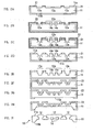
- FIGs. 2A to 2I show steps of the process for producing the mask 10.
- an oxide film (SiO 2 film) 21 that acts as a dry etching-resistive mask is deposited on the entire surface of the mask substrate 11.
- the oxide film 21 is deposited by steam thermal oxidation that involves leaving the mask substrate 11 in steam at 1,050°C.
- the material of the film to be deposited may be any material that functions as a mask against anisotropic etching described below. Examples of such a material include silicon nitride, silicon carbide, aluminum, and chromium.
- the deposition process may be vapor deposition, sputtering, plating, CVD, or the like.
- portions corresponding to the openings 12 are removed from the oxide film 21 on the surface of the mask substrate 11. These portions in the mask substrate 11 exposing the surface 11a as a result of the removal of the oxide film become the openings 12. These portions are referred to as "opening forming portions 12a”.
- a resist is applied on the mask substrate 11 to form a resist layer 22.
- Portions corresponding to the openings 12 but excluding portions corresponding to the beams 14 are then removed from the resist layer 22 on the surface 11a by photolithography.
- a resist is applied on the portions where the beams 14 are to be formed (hereinafter, these portions are referred to as the "beams forming portions 14a").
- the beams forming portions 14a are located inside the opening forming portions 12a exposed in the previous step. In this manner, each opening forming portion 12a is exposed as if it is divided into a plurality of segments.
- the mask substrate 11 is anisotropically etched in a particular direction, i.e., in a substantially orthogonal direction with respect to the surface 11a of the mask substrate 11.
- the silicon substrate is uniformly etched to a predetermined depth as a result.
- the silicon material in the portions corresponding to the openings 12 that do not include the portions corresponding to the beams 14 is etched away.
- the resist layer on the mask substrate 11 is removed by oxygen plasma treatment or the like.
- the mask substrate 11 without the resist is again anisotropically etched.
- the portion that has already been etched in the previous step is uniformly etched further.
- portions not covered with the oxide layer 21 are also etched to uniformly remove the silicon material in these portions.
- the resulting mask substrate 11 has two-step irregularities, as shown in Fig. 2E.
- the silicon portions etched for the first time in this step are the portions corresponding to the beams 14 (beams forming portions 14a). These portions are anisotropically etched to have a predetermined depth from the surface 11a of the mask substrate 11. As has been previously mentioned, the distance to the beams from the surface 11a is preferably about 5 ⁇ m or more.
- the oxide film 21 covering the mask substrate 11 is removed, and an oxide film 23 is formed to cover all the surfaces of the mask substrate 11, as shown in Fig. 2F.
- the oxide film 23 on a rear surface 11b of the mask substrate 11 is partly removed to expose central portion of the mask substrate 11, as shown in Fig. 2G
- the mask substrate 11 is wet-etched to a predetermined depth so as to uniformly remove the silicon material in the central portion of the mask substrate 11.
- anisotropic etching dry etching
- wet etching dry etching
- the oxide film 23 on the mask substrate 11 is removed to form a plurality of openings in the mask substrate 11, as shown in Fig. 2I.
- the openings in the mask substrate 11 are openings 12 (opening forming portions 12a).
- the portions a predetermined distance away from the surface 11a are the beams 14 (beams forming portions 14a).
- the openings 12 and the beams 14 are formed by conducting two or more etching steps at the surface 11a of the mask substrate 11.
- the reason for etching the rear surface 11b of the mask substrate 11 is to minimize the thickness of the mask 10.
- the reason for leaving the thick peripheral portion of the mask substrate 11 is to ensure the strength of the mask substrate 11.
- Fig. 3 shows the deposition process using the mask 10.
- Fig. 4 shows the pattern of the metal wiring 52 formed by the deposition process.
- the mask 10 is used to form a pattern, such as metal wiring 52, on the substrate 50 by physical vapor deposition, such as vapor-phase deposition or sputtering or by chemicophysical vapor deposition, such as CVD.
- the mask 10 is placed on the substrate 50 so that the surface 11a of the mask 10 is in contact with the substrate 50.
- a thin film of a predetermined material is then formed on the substrate 50 by physical vapor deposition or chemicophysical vapor deposition.
- the material deposits on the substrate 50 through the openings 12 in the mask 10. The material travels around the beams 14 and deposit on the entire exposed portions of the substrate 50 corresponding to the openings 12. Since the metal wiring 52 can be can be formed without being affected by the presence of the beams 14, a continuous pattern of the metal wiring 52 free of breaks can be formed.
- the closed pattern of the metal wiring 52 shown in Fig. 4 i.e., the pattern which has not been easily formed by the related art, can be advantageously formed.
- the distance from the surface 11a of the mask 10 to the beams 14 needs to be at least about 5 ⁇ m, as described above.
- the amount of the material that travels around the beams 14 decreases, and the pattern, such as metal wiring 52, formed on the substrate 50 becomes thin, thereby increasing the resistance or causing disconnection.
- a low-resistance metal wiring 52 may be formed by depositing an aluminum film, zincating the aluminum film, performing electroless nickel plating, and then performing electroless gold plating. In this manner, a metal wiring 52 having a low resistance can be formed with a smaller amount of expensive gold.
- the mask 10 used to form the patterned thin film may be reused by removing the material deposited on the rear surface 11b.
- the metal wiring 52 and the like can be formed at lower costs by the reuse of the mask 10.
- Fig. 5 is a side cross-sectional view of an organic EL device 100.
- the mask 10 includes pixel electrodes 130 acting as anodes, cathodes 180, and a plurality of pixel regions disposed between the anodes and the cathodes to form a matrix. Pixel regions include emission layers 160R, 160G, and 160B composed of organic materials.
- a circuit 120 for driving the pixel regions i.e., the emission layers 160R, 160G, and 160B, are disposed.
- the electrical wiring in the circuit 120 is formed by the above-described deposition process.
- the pixel electrodes 130 composed of indium tin oxide (ITO) or the like are disposed to form a matrix corresponding to the pixel regions.
- a hole injection layer 140 composed of copper phthalocyanine is disposed to cover the pixel electrodes 130 functioning as anodes.
- a hole transport layer 150 composed of N,N-di(naphthalyl)-N,N-diphenyl-benzidene (NPB) is disposed.
- each emission layer may be composed of a low molecular weight-organic material having a molecular weight of approximately 1,000 or less.
- each emission layer is composed of a host material, such as tris(8-hydroxyquinoline)aluminum (Alq3), and a dopant, such as rubrene.
- An electron injection layer 170 composed of lithium fluoride or the like is disposed to cover the emission layers 160.
- the cathodes 180 composed of aluminum or the like are disposed.
- a sealing substrate (not shown in the drawing) is bonded to the edges of the substrate 110 to hermetically seal the entire composite.
- Fig. 6 shows an electronic device according to one embodiment of the invention.
- the device is a cellular phone 200 including a display 201.
- Other examples of the device include a wrist watch-type electronic device having a display including a low molecular weight-organic EL device 100 and portable information processing devices, such as word processors and personal computers, that use the low molecular weight-organic EL device 100 as a display.
- the cellular phone 200 having the display 201 including the low molecular weight-organic EL device has high display contrast with high quality display.
Landscapes
- Chemical & Material Sciences (AREA)
- Engineering & Computer Science (AREA)
- Chemical Kinetics & Catalysis (AREA)
- Materials Engineering (AREA)
- Mechanical Engineering (AREA)
- Metallurgy (AREA)
- Organic Chemistry (AREA)
- Manufacturing & Machinery (AREA)
- Electroluminescent Light Sources (AREA)
- Physical Vapour Deposition (AREA)
Abstract
A mask (10) comprises a first portion (11d) having an opening (12) and a second portion (11c) disposed in the opening and surrounded by the opening. A beam connects the first portion (11d) to the second portion (11c). The method for producing such a mask comprises the steps of etching part of an opening forming portion not including a beam forming portion, the opening forming portion corresponding to the region where an opening is to be formed, and the beam forming portion corresponding to the region where a beam that divides the opening forming portion into a plurality of segments is to be formed, and the step of etching the entire opening forming portion in the same direction as in the preceding step. <IMAGE>
Description
The present invention generally relates to masks
for forming desired wiring patterns on substrates by vapor-phase
deposition or the like.
Techniques of forming electrical wiring on
substrates by photolithography and dry and wet etching have
been widely practiced. However, photolithographic processes
and etching processes require expensive equipment, and the
production costs are also high due to low yield and
administration costs required to control a plurality of
steps. Furthermore, use of large amounts of resists,
developing solutions, resist removers, and etching solutions
(gas) may cause environmental problems. When the substrates
are not flat, i.e., when holes and grooves are formed in the
substrates, it becomes difficult to form resist coatings or
high precision patterns.
In this connection, Japanese Unexamined Patent
Application Publication No. 4-236758 discloses a technique
of forming a desired wiring pattern on a substrate by vapor-phase
deposition while placing a substrate into close
contact with a patterned mask, such as a silicon wafer or
metal foil. This technique is particularly useful for
production of organic electroluminescence (EL) materials
which use large amounts of materials easily degradable by
moisture, oxygen, or the like.
However, application of this technique is limited
to masks with relatively simple patterns, such as
rectangular patterns and circular patterns. For example, it
is difficult to form complicated patterns, such as wiring
patterns, by this technique. In particular, this technique
is not suitable for forming a wiring pattern inside another
wiring pattern.
An advantage of the invention is to provide a mask
capable of forming a complicated circuit wiring pattern by
mask deposition, and a method for making such a mask.
According to an aspect of the invention, a mask
includes a first portion having an opening, a second portion
disposed in the opening and surrounded by the opening, and a
beam connecting the first portion to the second portion.
According to this aspect of the invention, an opening having
a complicated shape can be formed. For example, a closed
pattern can be formed. Furthermore, a continuous thin film
pattern may be formed on a substrate using this mask.
Particles of a material for forming a film can be deposited
on the substrate in an angled direction; thus, a mask having
finer openings can be formed.
Preferably, the thickness of the beam is smaller
than the thickness of other portions of the mask so that
particles of the material for making the thin film can reach
the substrate in an angled direction. Thus, a mask with a
finer pattern opening can be prepared. Preferably, the mask
is composed of silicon since the opening and the beam can be
formed with high reliability.
Another aspect of the invention provides a method
for producing.a mask for forming a patterned thin film on a
substrate. The method includes (a) etching part of an
opening forming portion not including a beam forming
portion, the opening forming portion corresponding to the
region where an opening is to be formed, and the beam
forming portion corresponding to the region where a beam
that divides the opening forming portion into a plurality of
segments is to be formed; and (b) etching the entire opening
forming portion in the same direction as in step (a).
According to this aspect, a mask that has a beam
connecting the side walls that define the opening and being
located at a predetermined distance away from a surface of
the mask can be formed with reliability.
The method may further include (c) etching the
mask in a different direction from that in steps (a) and (b)
to form an opening that penetrates the mask. In this
manner, the thickness and the strength of the mask can be
adequately adjusted. The mask is preferably composed of
silicon and anisotropic etching is preferably performed in
steps (a) and (b) so that an opening with a beam can be
reliably formed.
A yet another aspect of the invention provides a
method for depositing a patterned thin film on a substrate.
The method includes depositing a thin film using a mask
having a first portion having an opening, a second portion
disposed in the opening and surrounded by the opening, and a
beam connecting the first portion to the second portion.
According to this method, a patterned thin film having a
continuous complicated shape can be formed on the substrate.
The thin film is preferably a metal film. In this
manner, a continuous metal wiring can be formed. The metal
thin film is preferably composed of a plurality of types of
metal since the resistance of the metal wiring can be
reduced, and good electrical conduction can be ensured. The
mask is preferably reused by removing the material deposited
on the mask. In this manner, high-performance electronic
devices can be produced at low costs.
Another aspect of the invention provides an
electronic device including a metal wiring pattern prepared
as above. According to this aspect, continuous metal wiring
having a complicated shape can be produced at lower costs.
Thus, high performance electronic devices can be produced at
low costs.
Another aspect of the invention provides an
electronic apparatus having the electronic device described
above. According to this aspect, a high performance
electronic apparatus can be produced.
The invention will be described with reference to
the accompanying drawings, wherein like numbers reference
like elements, and wherein:
A mask, a method for making the mask, a deposition
method, an electronic device, and an electronic apparatus
according to various embodiments of the invention will now
be described with reference to the attached drawings.
Fig. 1 is a partial perspective cross-sectional
view showing a mask 10 used in forming a patterned thin film
on a substrate by a deposition process, a sputtering
process, a CVD process, or the like. The mask 10 includes a
mask substrate 11 composed of silicon and a plurality of
openings 12. An example of the shape of the pattern opening
12 is a line having a width of approximately 10 µm. When a
metal material is deposited on a substrate through this
pattern opening 12, a pattern, such as an electrical wiring,
having a width of approximately 10 µm can be formed. The
shape of the pattern opening 12 is not limited to lines and
may be circular, rectangular, or the like.
In each pattern opening 12, beams connecting
opposing side walls 13 of the pattern opening 12 are
disposed. The beams 14 are disposed at positions distant
from the opposing surface (hereinafter referred to as
"surface 11a") of the mask substrate 11. The distance
between the surface 11a and the beams 14 is at least 5 µm.
Since the beams 14 are disposed on the side walls 13 of the
pattern openings 12, it becomes possible to form closed
pattern openings in the mask substrate 11. For example, a
ring-shaped pattern opening 12 can be formed by suspending
the centerpiece using the beams 14. In particular, a
segment 11c of the mask substrate 11 in Fig. 1 is attached
to a segment 11d of the mask substrate 11 using the beams
14. Thus, the segment 11c does not separate from the mask
substrate 11, thereby forming part of the mask 10. Note
that the number of the beams 14 used may be suitably
adjusted according to the strength and the like of the
beams.
The reason for forming the beams 14 distant from
the surface 11a is to form continuous metal wiring on the
substrate without any break using the mask 10. In other
words, when the beams 14 are distant from the surface 11a,
for example, the material for the metal wiring can travel
around the beams to thereby sufficiently reach the desired
portion of the substrate. The steps of forming the metal
wiring will be described below.
The mask substrate 11 may be composed of metal,
glass, plastic, or the like. Preferably, the mask substrate
11 is a silicon plate, such as a silicon wafer, since
formation of the beams 14 are easier as will be described
below in connection with the production process. The mask
substrate 11 may be of any shape but preferably has a
thickness of several hundred micrometers.
The process for producing the mask 10 above will
now be described. Figs. 2A to 2I show steps of the process
for producing the mask 10.
First, an oxide film (SiO2 film) 21 that acts as a
dry etching-resistive mask is deposited on the entire
surface of the mask substrate 11. In particular, the oxide
film 21 is deposited by steam thermal oxidation that
involves leaving the mask substrate 11 in steam at 1,050°C.
The material of the film to be deposited may be any material
that functions as a mask against anisotropic etching
described below. Examples of such a material include
silicon nitride, silicon carbide, aluminum, and chromium.
The deposition process may be vapor deposition, sputtering,
plating, CVD, or the like.
Referring to Fig. 2A, portions corresponding to
the openings 12 are removed from the oxide film 21 on the
surface of the mask substrate 11. These portions in the
mask substrate 11 exposing the surface 11a as a result of
the removal of the oxide film become the openings 12. These
portions are referred to as "opening forming portions 12a".
Referring now to Fig. 2B, a resist is applied on
the mask substrate 11 to form a resist layer 22. Portions
corresponding to the openings 12 but excluding portions
corresponding to the beams 14 are then removed from the
resist layer 22 on the surface 11a by photolithography. In
other words, a resist is applied on the portions where the
beams 14 are to be formed (hereinafter, these portions are
referred to as the "beams forming portions 14a"). The beams
forming portions 14a are located inside the opening forming
portions 12a exposed in the previous step. In this manner,
each opening forming portion 12a is exposed as if it is
divided into a plurality of segments.
Next, the mask substrate 11 is anisotropically
etched in a particular direction, i.e., in a substantially
orthogonal direction with respect to the surface 11a of the
mask substrate 11. Referring now to Fig. 2C, the silicon
substrate is uniformly etched to a predetermined depth as a
result. In other words, the silicon material in the
portions corresponding to the openings 12 that do not
include the portions corresponding to the beams 14 (the
opening formation portions 12a other than the beams forming
portions 14a) is etched away.
Referring now to Fig. 2D, the resist layer on the
mask substrate 11 is removed by oxygen plasma treatment or
the like. The mask substrate 11 without the resist is again
anisotropically etched. As a result, the portion that has
already been etched in the previous step is uniformly etched
further. Among the portions exposed by the removal of the
resist, portions not covered with the oxide layer 21 are
also etched to uniformly remove the silicon material in
these portions. The resulting mask substrate 11 has two-step
irregularities, as shown in Fig. 2E.
Note that the silicon portions etched for the
first time in this step are the portions corresponding to
the beams 14 (beams forming portions 14a). These portions
are anisotropically etched to have a predetermined depth
from the surface 11a of the mask substrate 11. As has been
previously mentioned, the distance to the beams from the
surface 11a is preferably about 5 µm or more.
Next, the oxide film 21 covering the mask
substrate 11 is removed, and an oxide film 23 is formed to
cover all the surfaces of the mask substrate 11, as shown in
Fig. 2F. The oxide film 23 on a rear surface 11b of the
mask substrate 11 is partly removed to expose central
portion of the mask substrate 11, as shown in Fig. 2G
Referring now to Fig. 2H, the mask substrate 11 is
wet-etched to a predetermined depth so as to uniformly
remove the silicon material in the central portion of the
mask substrate 11. Here, anisotropic etching (dry etching)
may be performed instead of wet etching.
Lastly, the oxide film 23 on the mask substrate 11
is removed to form a plurality of openings in the mask
substrate 11, as shown in Fig. 2I. Of the openings in the
mask substrate 11, the openings in the surface 11a are
openings 12 (opening forming portions 12a). The portions a
predetermined distance away from the surface 11a are the
beams 14 (beams forming portions 14a).
As is described above, the openings 12 and the
beams 14 are formed by conducting two or more etching steps
at the surface 11a of the mask substrate 11. The reason for
etching the rear surface 11b of the mask substrate 11 is to
minimize the thickness of the mask 10. The reason for
leaving the thick peripheral portion of the mask substrate
11 is to ensure the strength of the mask substrate 11.
The process of forming a pattern, such as metal
wiring 52, on a substrate 50 using the mask 10 above will
now be described. Fig. 3 shows the deposition process using
the mask 10. Fig. 4 shows the pattern of the metal wiring
52 formed by the deposition process.
The mask 10 is used to form a pattern, such as
metal wiring 52, on the substrate 50 by physical vapor
deposition, such as vapor-phase deposition or sputtering or
by chemicophysical vapor deposition, such as CVD. In
particular, the mask 10 is placed on the substrate 50 so
that the surface 11a of the mask 10 is in contact with the
substrate 50. A thin film of a predetermined material is
then formed on the substrate 50 by physical vapor deposition
or chemicophysical vapor deposition. As shown in Fig. 3,
the material deposits on the substrate 50 through the
openings 12 in the mask 10. The material travels around the
beams 14 and deposit on the entire exposed portions of the
substrate 50 corresponding to the openings 12. Since the
metal wiring 52 can be can be formed without being affected
by the presence of the beams 14, a continuous pattern of the
metal wiring 52 free of breaks can be formed.
Accordingly, the closed pattern of the metal
wiring 52 shown in Fig. 4, i.e., the pattern which has not
been easily formed by the related art, can be advantageously
formed. Note that in order for the material for the thin
film to travel around the beams 14 and reach the surface of
the substrate 50, the distance from the surface 11a of the
mask 10 to the beams 14 needs to be at least about 5 µm, as
described above. At a shorter distance, the amount of the
material that travels around the beams 14 decreases, and the
pattern, such as metal wiring 52, formed on the substrate 50
becomes thin, thereby increasing the resistance or causing
disconnection.
In order to form the metal wiring 52 by forming a
patterned thin film on the substrate 50, two or more metal
materials are preferably deposited. For example, a low-resistance
metal wiring 52 may be formed by depositing an
aluminum film, zincating the aluminum film, performing
electroless nickel plating, and then performing electroless
gold plating. In this manner, a metal wiring 52 having a
low resistance can be formed with a smaller amount of
expensive gold.
The mask 10 used to form the patterned thin film
may be reused by removing the material deposited on the rear
surface 11b. The metal wiring 52 and the like can be formed
at lower costs by the reuse of the mask 10.
Fig. 5 is a side cross-sectional view of an
organic EL device 100. The mask 10 includes pixel
electrodes 130 acting as anodes, cathodes 180, and a
plurality of pixel regions disposed between the anodes and
the cathodes to form a matrix. Pixel regions include
emission layers 160R, 160G, and 160B composed of organic
materials.
On a surface of a substrate 110 composed of glass
or the like, a circuit 120 for driving the pixel regions,
i.e., the emission layers 160R, 160G, and 160B, are
disposed. Although the detailed structure of the circuit
120 is not shown in Fig. 5, the electrical wiring in the
circuit 120 is formed by the above-described deposition
process.
On the surface of the circuit 120, the pixel
electrodes 130 composed of indium tin oxide (ITO) or the
like are disposed to form a matrix corresponding to the
pixel regions. A hole injection layer 140 composed of
copper phthalocyanine is disposed to cover the pixel
electrodes 130 functioning as anodes. On the hole injection
layer 140, a hole transport layer 150 composed of N,N-di(naphthalyl)-N,N-diphenyl-benzidene
(NPB) is disposed.
On the hole transport layer 150, the emission
layers 160R, 160G, and 160B are disposed to form a matrix
corresponding to the pixel regions. Each emission layer may
be composed of a low molecular weight-organic material
having a molecular weight of approximately 1,000 or less.
In particular, each emission layer is composed of a host
material, such as tris(8-hydroxyquinoline)aluminum (Alq3),
and a dopant, such as rubrene.
An electron injection layer 170 composed of
lithium fluoride or the like is disposed to cover the
emission layers 160. On the surface of the electron
injection layer 170, the cathodes 180 composed of aluminum
or the like are disposed. A sealing substrate (not shown in
the drawing) is bonded to the edges of the substrate 110 to
hermetically seal the entire composite. When a voltage is
applied between the pixel electrodes 130 and the cathodes
180, holes are injected to the emission layers 160 through
the hole injection layer 140, and electrons are injected to
the emission layers 160 through the electron injection layer
170. Recombination of the holes and electrons occur in the
emission layers 160, thereby exciting the dopant and
achieving emission. The organic EL device 100 having the
emission layers 160 composed of organic materials has longer
lifetime and achieves higher emission efficiency.
Fig. 6 shows an electronic device according to one
embodiment of the invention. The device is a cellular phone
200 including a display 201. Other examples of the device
include a wrist watch-type electronic device having a
display including a low molecular weight-organic EL device
100 and portable information processing devices, such as
word processors and personal computers, that use the low
molecular weight-organic EL device 100 as a display.
The cellular phone 200 having the display 201
including the low molecular weight-organic EL device has
high display contrast with high quality display.
Although the invention has been described
heretofore by way of preferred embodiments with reference to
the attached drawings, the scope of the invention is not
limited to these embodiments. The shapes, combination, and
the like of the constituent elements described in the above
examples are mere examples, and various modifications and
alteration are possible depending on design matter without
departing from the scope of the invention.
Claims (12)
- A mask (10) comprising:a first portion (11c) having an opening (12);a second portion (11d) disposed in the opening and surrounded by the opening; anda beam (14) connecting the first portion (11c) to the second portion (11d).
- The mask according to claim 1, wherein the thickness of the beam (14) is smaller than the thickness of other portions (11; 11a, 11c, 11d) of the mask (10).
- The mask according to claim 1 or 2, wherein the mask (10) comprises silicon.
- A method for producing a mask for forming a patterned thin film on a substrate, the method comprising:(a) etching part of an opening forming portion not including a beam forming portion, the opening forming portion corresponding to the region where an opening is to be formed, and the beam forming portion corresponding to the region where a beam that divides the opening forming portion into a plurality of segments is to be formed; and(b) etching the entire opening forming portion in the same direction as in step (a).
- The method according to claim 4, further comprising:(c) etching the mask in a different direction to form an opening that penetrates the mask.
- The method according to claim 4 or 5, wherein the mask comprises silicon, and, in steps (a) and (b), anisotropic etching is performed.
- A method for depositing a patterned thin film on a substrate, the method comprising:depositing a thin film using a mask having a first portion having an opening, a second portion disposed in the opening and surrounded by the opening, and a beam connecting the first portion to the second portion.
- The method according to claim 7, wherein the thin film is a metal thin film.
- The method according to claim 8, wherein the metal thin film is prepared by depositing a plurality of types of metal.
- The method according to any of the claims 7 to 9, wherein the mask is reused by removing the material deposited on the mask.
- An electronic device comprising a metal wiring pattern prepared by the method according to any of the claims 7 to 10.
- An electronic apparatus comprising the electronic device according to claim 11.
Applications Claiming Priority (2)
| Application Number | Priority Date | Filing Date | Title |
|---|---|---|---|
| JP2004182459 | 2004-06-21 | ||
| JP2004182459A JP2006002243A (en) | 2004-06-21 | 2004-06-21 | Mask, mask manufacturing method, film forming method, electronic device, and electronic apparatus |
Publications (1)
| Publication Number | Publication Date |
|---|---|
| EP1609879A1 true EP1609879A1 (en) | 2005-12-28 |
Family
ID=34936863
Family Applications (1)
| Application Number | Title | Priority Date | Filing Date |
|---|---|---|---|
| EP05011197A Withdrawn EP1609879A1 (en) | 2004-06-21 | 2005-05-24 | Method for producing a mask |
Country Status (6)
| Country | Link |
|---|---|
| US (1) | US20050282368A1 (en) |
| EP (1) | EP1609879A1 (en) |
| JP (1) | JP2006002243A (en) |
| KR (1) | KR100767903B1 (en) |
| CN (1) | CN100389479C (en) |
| TW (1) | TWI310584B (en) |
Cited By (3)
| Publication number | Priority date | Publication date | Assignee | Title |
|---|---|---|---|---|
| WO2008068009A1 (en) * | 2006-12-06 | 2008-06-12 | Westfälische Wilhelms-Universität Münster | A universal method for selective area growth of organic molecules by vapor deposition |
| CN110872686A (en) * | 2018-08-29 | 2020-03-10 | 三星显示有限公司 | Mask assembly and apparatus and method for manufacturing a display device |
| WO2026077994A1 (en) * | 2024-10-09 | 2026-04-16 | Technische Universiteit Delft | Method of manufacturing a shadow mask for stencil lithography |
Families Citing this family (8)
| Publication number | Priority date | Publication date | Assignee | Title |
|---|---|---|---|---|
| JP4379394B2 (en) * | 2005-07-27 | 2009-12-09 | セイコーエプソン株式会社 | Mask and organic EL device manufacturing method |
| JP4692290B2 (en) * | 2006-01-11 | 2011-06-01 | セイコーエプソン株式会社 | Mask and film forming method |
| US8039532B2 (en) | 2007-08-16 | 2011-10-18 | Fujifilm Corporation | Heterocyclic compound, ultraviolet absorbent and composition containing the same |
| JP2011184720A (en) * | 2010-03-05 | 2011-09-22 | Ricoh Co Ltd | Mask for patterning and film forming device using the mask |
| CN101984135B (en) * | 2010-11-19 | 2013-07-10 | 光驰科技(上海)有限公司 | Film forming substrate clamp and film forming device thereof |
| US10562055B2 (en) | 2015-02-20 | 2020-02-18 | Si-Ware Systems | Selective step coverage for micro-fabricated structures |
| JP2017008342A (en) * | 2015-06-17 | 2017-01-12 | 株式会社ブイ・テクノロジー | Film deposition mask and production method of film deposition mask |
| CN110592526A (en) * | 2018-06-12 | 2019-12-20 | 张东晖 | Metal Evaporation Mask Structure |
Citations (6)
| Publication number | Priority date | Publication date | Assignee | Title |
|---|---|---|---|---|
| JPS59125667A (en) * | 1983-01-07 | 1984-07-20 | Nec Corp | Diode |
| US4715940A (en) * | 1985-10-23 | 1987-12-29 | Gte Products Corporation | Mask for patterning electrode structures in thin film EL devices |
| US5853805A (en) * | 1995-09-28 | 1998-12-29 | Murata Manufacturing Co., Ltd. | Apparatus and process for forming electrodes of electronic components |
| JPH1136061A (en) * | 1997-07-17 | 1999-02-09 | Mitsubishi Materials Corp | Masking jig for physical vapor deposition equipment |
| JP2000318334A (en) * | 1999-05-12 | 2000-11-21 | Tdk Corp | Metal mask for printing and manufacture thereof |
| JP2003282252A (en) * | 2002-03-26 | 2003-10-03 | Seiko Epson Corp | Method of manufacturing mask, method of manufacturing organic electroluminescence device, and organic electroluminescence device |
Family Cites Families (13)
| Publication number | Priority date | Publication date | Assignee | Title |
|---|---|---|---|---|
| US4004044A (en) * | 1975-05-09 | 1977-01-18 | International Business Machines Corporation | Method for forming patterned films utilizing a transparent lift-off mask |
| JPS5258606A (en) * | 1975-11-07 | 1977-05-14 | Hitachi Ltd | Printing metal mask |
| JPH0736361B2 (en) * | 1989-03-22 | 1995-04-19 | 株式会社村田製作所 | Resistive material, method for producing the same, and resistive paste using the same |
| JP3326088B2 (en) * | 1996-03-14 | 2002-09-17 | 株式会社東芝 | Semiconductor device and manufacturing method thereof |
| US6214413B1 (en) * | 1999-01-13 | 2001-04-10 | Applied Materials, Inc. | Method and apparatus for fabricating a wafer spacing mask on a substrate support chuck |
| EP1265994A2 (en) * | 2000-03-17 | 2002-12-18 | President And Fellows of Harvard College | Cell patterning technique |
| KR100631933B1 (en) * | 2000-06-28 | 2006-10-04 | 주식회사 하이닉스반도체 | How to make a stencil mask |
| JP3674573B2 (en) * | 2001-06-08 | 2005-07-20 | ソニー株式会社 | Mask, manufacturing method thereof, and manufacturing method of semiconductor device |
| JP2005086147A (en) * | 2003-09-11 | 2005-03-31 | Sony Corp | Metal single layer film forming method, wiring forming method, and field effect transistor manufacturing method |
| US6989327B2 (en) * | 2004-01-31 | 2006-01-24 | Hewlett-Packard Development Company, L.P. | Forming a contact in a thin-film device |
| US20050235845A1 (en) * | 2004-04-27 | 2005-10-27 | Hollis Michael R | Modular stencil system having interlocking stencils |
| US20060083927A1 (en) * | 2004-10-15 | 2006-04-20 | Zyvex Corporation | Thermal interface incorporating nanotubes |
| JP2006269599A (en) * | 2005-03-23 | 2006-10-05 | Sony Corp | Pattern forming method, organic field effect transistor manufacturing method, and flexible printed circuit board manufacturing method |
-
2004
- 2004-06-21 JP JP2004182459A patent/JP2006002243A/en active Pending
-
2005
- 2005-04-25 US US11/113,920 patent/US20050282368A1/en not_active Abandoned
- 2005-05-24 EP EP05011197A patent/EP1609879A1/en not_active Withdrawn
- 2005-06-07 TW TW094118774A patent/TWI310584B/en not_active IP Right Cessation
- 2005-06-07 CN CNB2005100758034A patent/CN100389479C/en not_active Expired - Fee Related
- 2005-06-20 KR KR1020050052814A patent/KR100767903B1/en not_active Expired - Fee Related
Patent Citations (6)
| Publication number | Priority date | Publication date | Assignee | Title |
|---|---|---|---|---|
| JPS59125667A (en) * | 1983-01-07 | 1984-07-20 | Nec Corp | Diode |
| US4715940A (en) * | 1985-10-23 | 1987-12-29 | Gte Products Corporation | Mask for patterning electrode structures in thin film EL devices |
| US5853805A (en) * | 1995-09-28 | 1998-12-29 | Murata Manufacturing Co., Ltd. | Apparatus and process for forming electrodes of electronic components |
| JPH1136061A (en) * | 1997-07-17 | 1999-02-09 | Mitsubishi Materials Corp | Masking jig for physical vapor deposition equipment |
| JP2000318334A (en) * | 1999-05-12 | 2000-11-21 | Tdk Corp | Metal mask for printing and manufacture thereof |
| JP2003282252A (en) * | 2002-03-26 | 2003-10-03 | Seiko Epson Corp | Method of manufacturing mask, method of manufacturing organic electroluminescence device, and organic electroluminescence device |
Non-Patent Citations (4)
| Title |
|---|
| PATENT ABSTRACTS OF JAPAN vol. 008, no. 250 (E - 279) 16 November 1984 (1984-11-16) * |
| PATENT ABSTRACTS OF JAPAN vol. 1999, no. 05 31 May 1999 (1999-05-31) * |
| PATENT ABSTRACTS OF JAPAN vol. 2000, no. 14 5 March 2001 (2001-03-05) * |
| PATENT ABSTRACTS OF JAPAN vol. 2003, no. 12 5 December 2003 (2003-12-05) * |
Cited By (6)
| Publication number | Priority date | Publication date | Assignee | Title |
|---|---|---|---|---|
| WO2008068009A1 (en) * | 2006-12-06 | 2008-06-12 | Westfälische Wilhelms-Universität Münster | A universal method for selective area growth of organic molecules by vapor deposition |
| CN110872686A (en) * | 2018-08-29 | 2020-03-10 | 三星显示有限公司 | Mask assembly and apparatus and method for manufacturing a display device |
| EP3617341A3 (en) * | 2018-08-29 | 2020-07-01 | Samsung Display Co., Ltd. | Mask assembly, and apparatus and method for manufacturing display apparatus including the mask assembly |
| US10903459B2 (en) | 2018-08-29 | 2021-01-26 | Samsung Display Co., Ltd. | Mask assembly, and apparatus and method for manufacturing display apparatus including the mask assembly |
| CN110872686B (en) * | 2018-08-29 | 2023-10-13 | 三星显示有限公司 | Mask assembly and apparatus and method for manufacturing display device |
| WO2026077994A1 (en) * | 2024-10-09 | 2026-04-16 | Technische Universiteit Delft | Method of manufacturing a shadow mask for stencil lithography |
Also Published As
| Publication number | Publication date |
|---|---|
| TW200603264A (en) | 2006-01-16 |
| CN1713342A (en) | 2005-12-28 |
| KR100767903B1 (en) | 2007-10-18 |
| TWI310584B (en) | 2009-06-01 |
| KR20060048438A (en) | 2006-05-18 |
| US20050282368A1 (en) | 2005-12-22 |
| CN100389479C (en) | 2008-05-21 |
| JP2006002243A (en) | 2006-01-05 |
Similar Documents
| Publication | Publication Date | Title |
|---|---|---|
| JP3948082B2 (en) | Method for manufacturing organic electroluminescence element | |
| JP6016407B2 (en) | Manufacturing method of organic EL display device | |
| CN1162052C (en) | Method for manufacturing organic electroluminescence display panel | |
| US7754274B2 (en) | Mask and method for manufacturing the same, method for manufacturing display, method for manufacturing organic electroluminescent display, organic electroluminescent device, and electronic device | |
| US7776645B2 (en) | Organic semiconductor device and its manufacturing method | |
| TWI745299B (en) | A shadow mask for organic light emitting diode manufacture | |
| US7470610B2 (en) | Method of fabricating organic electroluminescent devices | |
| KR100504472B1 (en) | organic electroluminescence device and fabricating method for the same | |
| JPH11339958A (en) | Method for manufacturing electroluminescent device | |
| EP1609879A1 (en) | Method for producing a mask | |
| US20030214232A1 (en) | Uniform deposition of organic layer | |
| KR100498087B1 (en) | Method of making organic electroluminescent display | |
| CN108365129B (en) | Display panel, manufacturing method thereof and display device | |
| CN112687825A (en) | Preparation method of OLED display panel and OLED display panel | |
| CN114657508B (en) | Mask assembly and method for manufacturing the mask assembly | |
| KR100337493B1 (en) | An Organic Electro-Luminescence Display Panel And Fabricating Method Thereof | |
| KR100437769B1 (en) | Fabrication Method for Organic Electroluminescence Decvice | |
| KR100768715B1 (en) | Organic electroluminescent device and manufacturing method thereof | |
| CN112670433A (en) | Method for preparing silicon-based OLED microdisplay anode by mask plate technology | |
| KR20060019977A (en) | Manufacturing method of organic thin film transistor and liquid crystal display device | |
| KR100684175B1 (en) | Manufacturing method of electroluminescent device | |
| KR101026804B1 (en) | Auxiliary electrode formation method of organic electroluminescent display | |
| KR100215798B1 (en) | Electroluminescent Device Manufacturing Method | |
| JPH05275549A (en) | Manufacture of semiconductor device | |
| KR102068964B1 (en) | array substrate for liquid crystal display device and fabricating method of the same |
Legal Events
| Date | Code | Title | Description |
|---|---|---|---|
| PUAI | Public reference made under article 153(3) epc to a published international application that has entered the european phase |
Free format text: ORIGINAL CODE: 0009012 |
|
| AK | Designated contracting states |
Kind code of ref document: A1 Designated state(s): AT BE BG CH CY CZ DE DK EE ES FI FR GB GR HU IE IS IT LI LT LU MC NL PL PT RO SE SI SK TR |
|
| AX | Request for extension of the european patent |
Extension state: AL BA HR LV MK YU |
|
| 17P | Request for examination filed |
Effective date: 20060628 |
|
| AKX | Designation fees paid |
Designated state(s): DE FR GB |
|
| STAA | Information on the status of an ep patent application or granted ep patent |
Free format text: STATUS: THE APPLICATION HAS BEEN WITHDRAWN |
|
| 18W | Application withdrawn |
Effective date: 20070719 |