EP1608210A1 - Wiring Board, Magnetic Disc Apparatus, and Method of Manufacturing Wiring Board - Google Patents
Wiring Board, Magnetic Disc Apparatus, and Method of Manufacturing Wiring Board Download PDFInfo
- Publication number
- EP1608210A1 EP1608210A1 EP05105312A EP05105312A EP1608210A1 EP 1608210 A1 EP1608210 A1 EP 1608210A1 EP 05105312 A EP05105312 A EP 05105312A EP 05105312 A EP05105312 A EP 05105312A EP 1608210 A1 EP1608210 A1 EP 1608210A1
- Authority
- EP
- European Patent Office
- Prior art keywords
- layer
- wiring board
- polyimide
- pattern
- polyimide layer
- Prior art date
- Legal status (The legal status is an assumption and is not a legal conclusion. Google has not performed a legal analysis and makes no representation as to the accuracy of the status listed.)
- Withdrawn
Links
- 238000004519 manufacturing process Methods 0.000 title claims description 16
- 239000004642 Polyimide Substances 0.000 claims abstract description 100
- 229920001721 polyimide Polymers 0.000 claims abstract description 100
- RYGMFSIKBFXOCR-UHFFFAOYSA-N Copper Chemical compound [Cu] RYGMFSIKBFXOCR-UHFFFAOYSA-N 0.000 claims abstract description 50
- 229910052802 copper Inorganic materials 0.000 claims abstract description 50
- 239000010949 copper Substances 0.000 claims abstract description 50
- 238000007747 plating Methods 0.000 claims abstract description 23
- 229910001220 stainless steel Inorganic materials 0.000 claims description 17
- 239000010935 stainless steel Substances 0.000 claims description 17
- 239000007788 liquid Substances 0.000 claims description 12
- 238000013007 heat curing Methods 0.000 claims description 7
- 239000011248 coating agent Substances 0.000 claims description 4
- 238000000576 coating method Methods 0.000 claims description 4
- 238000004891 communication Methods 0.000 description 8
- 238000000034 method Methods 0.000 description 8
- 239000004020 conductor Substances 0.000 description 6
- 230000008569 process Effects 0.000 description 6
- 229910000679 solder Inorganic materials 0.000 description 6
- 239000004840 adhesive resin Substances 0.000 description 5
- 229920006223 adhesive resin Polymers 0.000 description 5
- 238000005452 bending Methods 0.000 description 5
- 238000011161 development Methods 0.000 description 3
- 230000018109 developmental process Effects 0.000 description 3
- VYZAMTAEIAYCRO-UHFFFAOYSA-N Chromium Chemical compound [Cr] VYZAMTAEIAYCRO-UHFFFAOYSA-N 0.000 description 2
- PXHVJJICTQNCMI-UHFFFAOYSA-N Nickel Chemical compound [Ni] PXHVJJICTQNCMI-UHFFFAOYSA-N 0.000 description 2
- 230000008901 benefit Effects 0.000 description 2
- 230000008859 change Effects 0.000 description 2
- 238000006243 chemical reaction Methods 0.000 description 2
- 229910052804 chromium Inorganic materials 0.000 description 2
- 239000011651 chromium Substances 0.000 description 2
- 238000006073 displacement reaction Methods 0.000 description 2
- 238000003754 machining Methods 0.000 description 2
- 239000000463 material Substances 0.000 description 2
- 238000000059 patterning Methods 0.000 description 2
- 229920002120 photoresistant polymer Polymers 0.000 description 2
- 230000001737 promoting effect Effects 0.000 description 2
- 230000003014 reinforcing effect Effects 0.000 description 2
- 239000000853 adhesive Substances 0.000 description 1
- 230000001070 adhesive effect Effects 0.000 description 1
- 230000015572 biosynthetic process Effects 0.000 description 1
- 230000007797 corrosion Effects 0.000 description 1
- 238000005260 corrosion Methods 0.000 description 1
- 230000006378 damage Effects 0.000 description 1
- 239000000428 dust Substances 0.000 description 1
- 230000000694 effects Effects 0.000 description 1
- 238000005530 etching Methods 0.000 description 1
- 238000002474 experimental method Methods 0.000 description 1
- 230000009477 glass transition Effects 0.000 description 1
- 230000001771 impaired effect Effects 0.000 description 1
- 230000006872 improvement Effects 0.000 description 1
- FBAFATDZDUQKNH-UHFFFAOYSA-M iron chloride Chemical compound [Cl-].[Fe] FBAFATDZDUQKNH-UHFFFAOYSA-M 0.000 description 1
- 239000000203 mixture Substances 0.000 description 1
- 238000012986 modification Methods 0.000 description 1
- 230000004048 modification Effects 0.000 description 1
- 229910052759 nickel Inorganic materials 0.000 description 1
- 238000012545 processing Methods 0.000 description 1
- 230000009467 reduction Effects 0.000 description 1
- 230000007261 regionalization Effects 0.000 description 1
- 229920005989 resin Polymers 0.000 description 1
- 239000011347 resin Substances 0.000 description 1
- 230000008054 signal transmission Effects 0.000 description 1
- 239000000126 substance Substances 0.000 description 1
- 239000013585 weight reducing agent Substances 0.000 description 1
- 238000001039 wet etching Methods 0.000 description 1
Images



Classifications
-
- H—ELECTRICITY
- H05—ELECTRIC TECHNIQUES NOT OTHERWISE PROVIDED FOR
- H05K—PRINTED CIRCUITS; CASINGS OR CONSTRUCTIONAL DETAILS OF ELECTRIC APPARATUS; MANUFACTURE OF ASSEMBLAGES OF ELECTRICAL COMPONENTS
- H05K3/00—Apparatus or processes for manufacturing printed circuits
- H05K3/22—Secondary treatment of printed circuits
- H05K3/28—Applying non-metallic protective coatings
-
- H—ELECTRICITY
- H05—ELECTRIC TECHNIQUES NOT OTHERWISE PROVIDED FOR
- H05K—PRINTED CIRCUITS; CASINGS OR CONSTRUCTIONAL DETAILS OF ELECTRIC APPARATUS; MANUFACTURE OF ASSEMBLAGES OF ELECTRICAL COMPONENTS
- H05K1/00—Printed circuits
- H05K1/02—Details
- H05K1/03—Use of materials for the substrate
- H05K1/0313—Organic insulating material
- H05K1/032—Organic insulating material consisting of one material
- H05K1/0346—Organic insulating material consisting of one material containing N
-
- H—ELECTRICITY
- H05—ELECTRIC TECHNIQUES NOT OTHERWISE PROVIDED FOR
- H05K—PRINTED CIRCUITS; CASINGS OR CONSTRUCTIONAL DETAILS OF ELECTRIC APPARATUS; MANUFACTURE OF ASSEMBLAGES OF ELECTRICAL COMPONENTS
- H05K1/00—Printed circuits
- H05K1/02—Details
- H05K1/03—Use of materials for the substrate
- H05K1/05—Insulated conductive substrates, e.g. insulated metal substrate
- H05K1/056—Insulated conductive substrates, e.g. insulated metal substrate the metal substrate being covered by an organic insulating layer
-
- H—ELECTRICITY
- H05—ELECTRIC TECHNIQUES NOT OTHERWISE PROVIDED FOR
- H05K—PRINTED CIRCUITS; CASINGS OR CONSTRUCTIONAL DETAILS OF ELECTRIC APPARATUS; MANUFACTURE OF ASSEMBLAGES OF ELECTRICAL COMPONENTS
- H05K2201/00—Indexing scheme relating to printed circuits covered by H05K1/00
- H05K2201/01—Dielectrics
- H05K2201/0137—Materials
- H05K2201/0154—Polyimide
-
- H—ELECTRICITY
- H05—ELECTRIC TECHNIQUES NOT OTHERWISE PROVIDED FOR
- H05K—PRINTED CIRCUITS; CASINGS OR CONSTRUCTIONAL DETAILS OF ELECTRIC APPARATUS; MANUFACTURE OF ASSEMBLAGES OF ELECTRICAL COMPONENTS
- H05K3/00—Apparatus or processes for manufacturing printed circuits
- H05K3/0011—Working of insulating substrates or insulating layers
- H05K3/0017—Etching of the substrate by chemical or physical means
- H05K3/0023—Etching of the substrate by chemical or physical means by exposure and development of a photosensitive insulating layer
-
- H—ELECTRICITY
- H05—ELECTRIC TECHNIQUES NOT OTHERWISE PROVIDED FOR
- H05K—PRINTED CIRCUITS; CASINGS OR CONSTRUCTIONAL DETAILS OF ELECTRIC APPARATUS; MANUFACTURE OF ASSEMBLAGES OF ELECTRICAL COMPONENTS
- H05K3/00—Apparatus or processes for manufacturing printed circuits
- H05K3/10—Apparatus or processes for manufacturing printed circuits in which conductive material is applied to the insulating support in such a manner as to form the desired conductive pattern
- H05K3/108—Apparatus or processes for manufacturing printed circuits in which conductive material is applied to the insulating support in such a manner as to form the desired conductive pattern by semi-additive methods; masks therefor
Definitions
- the present invention relates to a wiring board and a method of manufacturing the same, as well as a magnetic disc apparatus having the wiring board and, more particularly, to a wiring board that is preferable for a small-sized magnetic disc apparatus and a method of manufacturing the same, as well as a magnetic disc apparatus having such a wiring board.
- miniaturization is required also in a magnetic disc apparatus as a representative apparatus for storing a large volume of digital information.
- a magnetic disc apparatus For such a small magnetic disc apparatus, the size of a disc enclosure itself accommodating a disc and so on is small, and each wiring board equipped therein is also required to respond to miniaturization. Additionally, not only to respond to miniaturization, it is also important to ensure reliability.
- wiring boards used and disposed inside the disc enclosures are functionally required to have flexibility.
- a wiring board as a cable extendingly provided on a carriage in order to exchange signals with a head and the like on the carriage. Since the carriage is displaced with the head over a magnetic disc, according thereto a state of bending of the wiring board which is extendingly provided changes drastically. Therefore, as for the reliability thereof, it is necessary to be considered more carefully than in a case of normal use inwhich the state of bending does not change.
- stiffness is preferable to be small in order to avoid being a disturbance element (load) as far as possible in displacement of the carriage.
- the flexible wiring board features a cover lay in particular, and there is referred to the improvement of physical, chemical, and mechanical properties of the cover lay.
- Patent Document 1 Japanese Patent Laid-Open (Kokai) Application No. 2003-149804
- the present invention is made in consideration of the circumstances described above, and in a wiring board and a method of manufacturing the same as well as a magnetic disc apparatus having the wiring board, it is an object of the present invention to provide: a wiring board which can be applied to the magnetic disc apparatus and is capable of promoting miniaturization and ensuring reliability; a method of manufacturing the same; and a magnetic disc apparatus having such a wiring board.
- a wiring board includes: a first polyimide layer of heat-cured photosensitive polyimide; a copper layer pattern formed by growing an electrolytic copper layer on the first polyimide layer; and a second polyimide layer of heat-cured photosensitive polyimide, the second polyimide layer covering the formed copper layer pattern.
- this wiring board an insulating layer on the copper layer pattern is formed by heat-curing the photosensitive polyimide. Therefore, a fine pattern is easily formed by a photo mask, and a polyimide layer can be formed, for example, between narrow pitch lands. Hereby, faulty connections at the time of component mounting can be reduced. Additionally, the entire wiring board is thin, and so a degree to become a load in bending is smaller. Further, since a structure is simple, the structure is hard to be destroyed. Consequently, this wiring board is suitable to be applied to a magnetic disc apparatus to realize miniaturization and to ensure reliability.
- a magnetic disc apparatus includes: a wiring board which has a first polyimide layer of heat-cured photosensitive polyimide, a copper layer pattern formed by growing an electrolytic copper layer on the first polyimide layer, and a second polyimide layer of heat-cured photosensitive polyimide, the second polyimide layer covering the formed copper layer pattern; a head carriage having an electric connection to the wiring board and having a head mounted thereon to perform input/output of electric signals transmitted bilaterally via the connection; and a magnetic disc on which reading/writing of magnetic information are performed by the head mounted on the head carriage.
- this magnetic disc apparatus uses the above-described wiring board as a wiring board as a cable to be connected to the head carriage. Therefore, as the disc apparatus, miniaturization is realized and reliability is ensured.
- a method of manufacturing the wiring board according to an aspect of the present invention includes: applying first liquid photosensitive polyimide on a stainless steel layer by coating; forming a first polyimide layer of a predetermined shape pattern by exposing, developing, and heat-curing the applied first liquid photosensitive polyimide; growing an electrolytic copper plating layer of a predetermined pattern on the formed first polyimide layer; applying second liquid photosensitive polyimide on the first polyimide layer including the electrolytic copper plating layer of the predetermined pattern by coating; and forming a second polyimide layer of a predetermined pattern by exposing, developing, and heat-curing the applied second liquid photosensitive polyimide so that a part of the electrolytic copper plating layer is exposed.
- This manufacturing method is an example of manufacturing the above-described wiring board.
- a wiring board applied to a magnetic disc apparatus capable of promoting miniaturization and ensuring reliability, a method of manufacturing the same, and a magnetic disc apparatus having such a wiring board.
- a stainless steel layer provided on a surface of the first polyimide layer different from a side having the copper layer pattern. This is a structure in which the stainless steel layer is included as a mechanical reinforcing layer.
- the second polyimide layer may have plural openings to expose a part of the copper layer pattern. This is a case that the openings are used, for example, as lands for mounting components.
- the plural openings of the second polyimide layer respectively may be openings for separate electrical nodes in the copper layer pattern. More specifically, since the openings can be provided by a fine pattern, the opening is provided for each electrically separate node of the copper layer pattern. Hereby, short-circuit faults of solder which may occur between those exposed nodes can be effectively reduced.
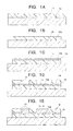
- Fig. 1A to Fig. 1E as well as Fig. 2A to Fig. 2E are process drawings showing a manufacturing process of a wiring board according to one embodiment of the present invention by way of schematic cross sections.
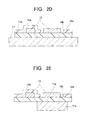
- Fig. 2A to Fig. 2E are drawings continued from Fig. 1E, steps progress respectively in sequence from A in the drawings.
- the same or substantially the same portions are represented by the same reference numerals and symbols.
- the wiring board of the present embodiment In order to manufacture the wiring board of the present embodiment, first, using a prepared stainless steel plate, while the stainless steel plate is passed between two rollers having a predetermined gap, for example, liquid photosensitive polyimide is applied on an entire surface thereof.
- a photosensitive polyimide layer 12 with a predetermined thickness applied on the stainless steel layer 11.
- the stainless steel layer 11 also functions as a base material (base) at a time of manufacturing this wiring board, and thickness thereof is, for example, from about 25 ⁇ m to about 100 ⁇ m. Thickness of the photosensitive polyimide layer 12 is, for example, about 10 ⁇ m.
- the photosensitive polyimide layer 12 obtained by applying is patterned in a predetermined pattern so that a patterned polyimide layer 12a is obtained.
- a photo mask of a predetermined pattern is disposed on the photosensitive polyimide layer 12 and then predetermined light is irradiated thereon, so that exposure of the photosensitive polyimide layer 12 is performed. Thereafter, the photo mask is removed and respective development and heat-curing processes are performed on the exposed photosensitive polyimide layer 12.
- the patterned polyimide layer 12a obtained hereby functions as a base layer in the wiring board, and a shape thereof is determined by the photo mask so that one having a fine portion can be easily manufactured.
- a seed layer (for example, chromium for a base, and copper thereon) 13 for electrolytic copper plating is formed in thickness of, for example, the chromium being about 0.01 ⁇ m to about 0.05 ⁇ m and thickness of the copper being about 0.1 ⁇ m to about 0.5 ⁇ m, on the entire surface of the patterned polyimide layer 12a.
- a resist 14 of a predetermined pattern is formed on the formed seed layer 13.
- the predetermined pattern here is a pattern for forming an electric conductor (copper layer) pattern.
- the resist 14 can be formed using, for example, a known photo resist (in the form of liquid or sheet: the one in the form of sheet is advantageous for a fine pattern).
- a step of electrolytic copper plating is performed using the seed layer 13 as an electric current supply channel, and as shown in Fig. 1E, an electrolytic copper plating layer 15 is grown on portions without the resist 14 on the seed layer 13. Thickness to be obtained after growing is, for example, about 12 ⁇ m.
- the electrolytic copper plating layer 15 is formed, the resist 14 is removed as shown in Fig. 2A, and in addition, as shown in Fig. 2B, the seed layer 13 is removed by wet etching, for example.
- an electric conductor (copper layer) pattern by the electrolytic copper plating layer 15 is obtained.
- nickel plating (not shown) for corrosion control may be applied on a surface of the electrolytic copper plating layer 15.
- the electric conductor pattern obtained here can be used as a wiring pattern or a land for mounting components.
- a cross section thereof is close to rectangular in shape as shown in the drawing, and therefore there is an advantage that the wiring pattern can have higher allowable current density than a wiring pattern formed by etching if they have the same areas in plan views.
- liquid photosensitive polyimide is applied as in applying and forming of the photosensitive polyimide layer 12 so that a photosensitive polyimide layer 16 is obtained.
- the same composition as that for the photosensitive polyimide layer 12 can be used.
- Formed thickness of the photosensitive polyimide layer 16 is, for example, about 5 ⁇ m.
- the photosensitive polyimide layer 16 obtained by applying is patterned to a predetermined pattern so that a patterned polyimide layer 16a is obtained.
- a photo mask of a predetermined pattern is disposed on the photosensitive polyimide layer 16 and predetermined light is irradiated so that exposure of the photosensitive polyimide layer 16 is performed. Thereafter, the photo mask is removed and respective development and heat-curing processes are performed on the exposed photosensitive polyimide layer 16.
- the patterned polyimide layer 16a obtained here functions as a cover layer in the wiring board.
- a part of the electrolytic copper plating layer 15 becomes in an exposed state by an opening 16b of the polyimide layer 16a.
- the electrolytic copper plating layer 15 of this exposed part can be used as, for example, a component mounting land or a connecting electrode to a connector. Since a pattern of the opening is determined by the photo mask, one having a fine portion can also be easily manufactured.
- the stainless steel layer 11 is patterned to a predetermined pattern so that a patterned stainless steel layer 11a is obtained.
- a resist of a predetermined pattern is formed on the stainless steel layer 11 (opposite side of the polyimide layer 12a side), and with this resist being a mask the stainless steel layer 11 is wet etched by, for example, iron chloride.
- This resist can be formed using, for example, a known photo resist (in the form of liquid or sheet: the one in the form of sheet is advantageous for a fine pattern).
- the stainless steel layer 11a left in the patterning functions as a mechanical reinforcing layer, for example, in this wiring board structure.
- the wiring board manufactured according to the above is constituted, except the stainless steel layer 11a, with the polyimide layer 12a as the base layer, the electrolytic copper plating layer 15 as the electric conductor (copper layer) pattern, and the polyimide layer 16a as the cover layer, and hence the structure thereof is very simple.
- a temperature range for use is not limited by a glass transition point of the adhesive resin layer, and the wiring board has a wide usable temperature. According to an experiment, a large characteristic change is not recognized until the parts of polyimide layers 12a, 16a show weight reduction at 450°C.
- the polyimide layer 16a as the cover layer in particular is obtained by way of patterning by exposure and development, formation accuracy thereof is very high. Therefore, there is no need for high bonding accuracy that is required in a conventionally well-known method, such as a method of bonding a polyimide layer on which an opening is formed in advance with bonding resin. Also, productivity thereof is higher than that in a case of forming the opening by laser machining after polyimide layers are bonded. In the case of laser machining, there is also a restriction that the opening must be in the region where the layer under the polyimide layer 16 is the electrolytic copper plating layer 15.
- the opening 16b corresponding to the land or electrode can be formed highly productively.
- the opening 16b of the polyimide layer 16a can be easily formed even if the opening is smaller than 0.4 mm in diameter.
- the adhesive resin tends to come off from the polyimide layer in that fine portion. For example, such coming off is prominent when a distance between the openings of the polyimide layer is less than 0.25 mm. In such a case, an adhesive failure occurs.
- the polyimide layer must be structured such that an opening is provided collectively for separate electrical nodes, but this tends to cause short-circuiting of solder between the nodes at the time of component mounting. It is because there is no dam effect for melted solder by the polyimide layer.
- a res ist material is further provided between the nodes, but this undeniably complicates the process. In the above embodiment, such disadvantages are completely eliminated.
- the electrolytic copper plating layer 15 is used as the wiring pattern, flexibility as in a case that rolled copper is used can be ensured by making the thickness thereof considerably thin.
- this wiring board can be applied also to the use in which high flexibility is required. This relates to the fact that the entire wiring board is formed to be thin in a simple layer structure.
- Fig. 3 is a top view showing an aspect in which the wiring board according to the one embodiment of the present invention is used in the magnetic disc apparatus.
- this magnetic disc apparatus includes: a magnetic disc 31; a disc clamper 32; a head carriage 33; a head 34; a pivot 35, a voice coil motor 36; and a head carriage communication wiring board 37.
- the size as a whole is, for example, 32 mm long and 24 mm wide.
- the magnetic disc 31 is a disc-shaped medium retaining information as a magnetic pattern in a circumferential direction, magnetic signals being written/read by the head 34 provided at an end of the head carriage 33 that is displaced in a radial direction of the medium.
- the disc clamper 32 is for screwing and fixing a rotation center of the magnetic disc 31 to a spindle motor (not shown) side that is provided underneath thereof.
- the head carriage 33 is for displacing the head 34 provided on its end in the radial direction while keeping the head floated over the magnetic disc 31.
- the head 34 is for performing conversion of the electrical signal/magnetic signal to write information into the magnetic disc 31, and conversion of the magnetic signal/electrical signal to read information from the magnetic disc 31.
- the electrical signals of writing/reading are transmitted bilaterally from the head carriage communication wiring board 37 having a connection to the head carriage 33.
- the pivot 35 is for supporting the head carriage 33 rotatably as a displacement (rotation) center of the head carriage 33.
- the voice coil motor 36 is for being a driving source to make the head carriage 33 rotate around the pivot 35.
- the head carriage communication wiring board 37 is communicated (connected) to the head carriage 33 and is for transmitting the signals exchanged bilaterally with the head 34.
- the signal may include a signal to the voice coil motor 36.
- the wiring board has a portion which functions mainly as a cable for signal transmission and whose state of bending changes according to the rotation of the head carriage 33, as well as a region which is continued to the portion in a shape-fixed state and for mainly mounting components (components being not shown).
- the head carriage communication wiring board 37 is the wiring board according to the embodiment described above.
- a degree of load at the time that the head carriage 33 is displaced is smaller due to the thinness thereof as a whole.
- the stacked structure is simple, structural destruction is hard to occur and reliability is ensured.
- the polyimide layer as the cover layer has the opening for each finely disposed land for mounting components, there is effectively reduced the occurrence of the faulty connection such as short-circuitingof solder at the time of mounting components.
- conditions necessary for application to a small-sized magnetic disc apparatus is fulfilled.
- Fig. 4 is a top view showing a structure of only the head carriage communication wiring board 37 shown in Fig. 3.
- a stainless steel layer 37b i.e. the patterned stainless steel layer 11a in Fig. 2E
- the purpose thereof is to increase mechanical stiffness since flexibility is not required in such regions.
- lands 37a for mounting components are exposed. Though not shown, between these lands 37a as well as in a portion as a cable to the head carriage 33 side, a wiring pattern by the electrolytic copper plating layer is formed.
- Fig. 5 is a top view enlargedly showing a structure of the component mounting region in the head carriage communication wiring board 37 shown in Fig. 4.
- the respective lands 37a for mounting components are separately exposed by the openings 16b of the polyimide layer 16a of the upper surface.
- the lands 37a correspond to the electrolytic copper plating layer 15 in Fig. 2E. Since the lands 37a are separately exposed by the openings 16b, the polyimide layer 16a exhibits a function to dam melted solder in the step of mounting components. Hereby, occurrences of fault such as short-circuiting of solder can be effectively reduced.
Landscapes
- Engineering & Computer Science (AREA)
- Manufacturing & Machinery (AREA)
- Microelectronics & Electronic Packaging (AREA)
- Insulated Metal Substrates For Printed Circuits (AREA)
- Adjustment Of The Magnetic Head Position Track Following On Tapes (AREA)
- Moving Of Heads (AREA)
- Manufacturing Of Printed Wiring (AREA)
Abstract
Disclosed is a wiring board including a first polyimide layer (12) of heat-cured photosensitive polyimide, a copper layer pattern (15) formed by growing an electrolytic copper plating layer on the polyimide layer, and a second polyimide layer (16) of heat-cured photosensitive polyimide, the second polyimide layer covering the copper layer pattern. Also, disclosed is a magnetic disc apparatus including this wiring board (37), a head carriage (33) having an electric connection to the wiring board and having a head (34) mounted thereon to perform input/output of electric signals transmitted bilaterally via the connection, and a magnetic disc (31) on which reading/writing of magnetic information are performed by the head mounted on the head carriage. <IMAGE>
Description
This application is based upon and claims the benefit of
priority from the prior Japanese Patent Application No. 2004-181181,
filed on June 18, 2004; the entire contents of which are incorporated
herein by reference.
The present invention relates to a wiring board and a method
of manufacturing the same, as well as a magnetic disc apparatus having
the wiring board and, more particularly, to a wiring board that is
preferable for a small-sized magnetic disc apparatus and a method
of manufacturing the same, as well as a magnetic disc apparatus having
such a wiring board.
Along with the sophistication in performance and the reduction
in size and weight of portable devices and electronic devices,
miniaturization is required also in a magnetic disc apparatus as
a representative apparatus for storing a large volume of digital
information. For such a small magnetic disc apparatus, the size
of a disc enclosure itself accommodating a disc and so on is small,
and each wiring board equipped therein is also required to respond
to miniaturization. Additionally, not only to respond to
miniaturization, it is also important to ensure reliability.
Some of wiring boards used and disposed inside the disc
enclosures are functionally required to have flexibility. As a
representative of such a wiring board, there is a wiring board as
a cable extendingly provided on a carriage in order to exchange signals
with a head and the like on the carriage. Since the carriage is
displaced with the head over a magnetic disc, according thereto a
state of bending of the wiring board which is extendingly provided
changes drastically. Therefore, as for the reliability thereof,
it is necessary to be considered more carefully than in a case of
normal use inwhich the state of bending does not change. Incidentally,
stiffness is preferable to be small in order to avoid being a
disturbance element (load) as far as possible in displacement of
the carriage.
As for miniaturization, it is necessary to respond to a trend
that a pitch between lands in a component mounting region of the
wiring board that is used is becoming increasingly narrower. If
the pitch is narrow, a faulty connection easily occurs at a time
of component mounting and reliability may be impaired. In this way,
in the small-sized magnetic disc apparatus, two opposite things are
always required of the wiring board used therein, to respond to
miniaturization and to ensure reliability. Incidentally, as an
example that could be used as such a flexible wiring board having
a narrow pitch and high reliability, there is one described in Patent
Document 1 stated below. As for the content of the patent document,
the flexible wiring board features a cover lay in particular, and
there is referred to the improvement of physical, chemical, and
mechanical properties of the cover lay.
The present invention is made in consideration of the
circumstances described above, and in a wiring board and a method
of manufacturing the same as well as a magnetic disc apparatus having
the wiring board, it is an object of the present invention to provide:
a wiring board which can be applied to the magnetic disc apparatus
and is capable of promoting miniaturization and ensuring reliability;
a method of manufacturing the same; and a magnetic disc apparatus
having such a wiring board.
A wiring board according to an aspect of the present invention
includes: a first polyimide layer of heat-cured photosensitive
polyimide; a copper layer pattern formed by growing an electrolytic
copper layer on the first polyimide layer; and a second polyimide
layer of heat-cured photosensitive polyimide, the second polyimide
layer covering the formed copper layer pattern.
More specifically, in this wiring board, an insulating layer
on the copper layer pattern is formed by heat-curing the
photosensitive polyimide. Therefore, a fine pattern is easily
formed by a photo mask, and a polyimide layer can be formed, for
example, between narrow pitch lands. Hereby, faulty connections
at the time of component mounting can be reduced. Additionally,
the entire wiring board is thin, and so a degree to become a load
in bending is smaller. Further, since a structure is simple, the
structure is hard to be destroyed. Consequently, this wiring board
is suitable to be applied to a magnetic disc apparatus to realize
miniaturization and to ensure reliability.
A magnetic disc apparatus according to an aspect of the present
invention includes: a wiring board which has a first polyimide layer
of heat-cured photosensitive polyimide, a copper layer pattern formed
by growing an electrolytic copper layer on the first polyimide layer,
and a second polyimide layer of heat-cured photosensitive polyimide,
the second polyimide layer covering the formed copper layer pattern;
a head carriage having an electric connection to the wiring board
and having a head mounted thereon to perform input/output of electric
signals transmitted bilaterally via the connection; and a magnetic
disc on which reading/writing of magnetic information are performed
by the head mounted on the head carriage.
More specifically, this magnetic disc apparatus uses the
above-described wiring board as a wiring board as a cable to be
connected to the head carriage. Therefore, as the disc apparatus,
miniaturization is realized and reliability is ensured.
A method of manufacturing the wiring board according to an
aspect of the present invention includes: applying first liquid
photosensitive polyimide on a stainless steel layer by coating;
forming a first polyimide layer of a predetermined shape pattern
by exposing, developing, and heat-curing the applied first liquid
photosensitive polyimide; growing an electrolytic copper plating
layer of a predetermined pattern on the formed first polyimide layer;
applying second liquid photosensitive polyimide on the first
polyimide layer including the electrolytic copper plating layer of
the predetermined pattern by coating; and forming a second polyimide
layer of a predetermined pattern by exposing, developing, and
heat-curing the applied second liquid photosensitive polyimide so
that a part of the electrolytic copper plating layer is exposed.
This manufacturing method is an example of manufacturing the
above-described wiring board.
According to the present invention, there can be provided
a wiring board applied to a magnetic disc apparatus and capable of
promoting miniaturization and ensuring reliability, a method of
manufacturing the same, and a magnetic disc apparatus having such
a wiring board.
Embodiments of the present invention will be described with
reference to the drawings, but these drawings are presented only
for the illustrative purpose and in no respect, are intended to Iimit
the present invention.
As a form of an embodiment of the present invention, there
may be further included a stainless steel layer provided on a surface
of the first polyimide layer different from a side having the copper
layer pattern. This is a structure in which the stainless steel
layer is included as a mechanical reinforcing layer.
As another form, the second polyimide layer may have plural
openings to expose a part of the copper layer pattern. This is a
case that the openings are used, for example, as lands for mounting
components.
As still another form, the plural openings of the second
polyimide layer respectively may be openings for separate electrical
nodes in the copper layer pattern. More specifically, since the
openings can be provided by a fine pattern, the opening is provided
for each electrically separate node of the copper layer pattern.
Hereby, short-circuit faults of solder which may occur between those
exposed nodes can be effectively reduced.
Based on the above, embodiments of the present invention will
be hereinafter described with reference to the drawings. Fig. 1A
to Fig. 1E as well as Fig. 2A to Fig. 2E are process drawings showing
a manufacturing process of a wiring board according to one embodiment
of the present invention by way of schematic cross sections. Fig.
2A to Fig. 2E are drawings continued from Fig. 1E, steps progress
respectively in sequence from A in the drawings. In these drawings,
the same or substantially the same portions are represented by the
same reference numerals and symbols.
In order to manufacture the wiring board of the present
embodiment, first, using a prepared stainless steel plate, while
the stainless steel plate is passed between two rollers having a
predetermined gap, for example, liquid photosensitive polyimide is
applied on an entire surface thereof. Hereby, as shown in Fig. 1A,
there is obtained a photosensitive polyimide layer 12 with a
predetermined thickness applied on the stainless steel layer 11.
The stainless steel layer 11 also functions as a base material (base)
at a time of manufacturing this wiring board, and thickness thereof
is, for example, from about 25 µm to about 100 µm. Thickness of
the photosensitive polyimide layer 12 is, for example, about 10 µm.
As shown in Fig. 1B, the photosensitive polyimide layer 12
obtained by applying is patterned in a predetermined pattern so that
a patterned polyimide layer 12a is obtained. For this, for example,
a photo mask of a predetermined pattern is disposed on the
photosensitive polyimide layer 12 and then predetermined light is
irradiated thereon, so that exposure of the photosensitive polyimide
layer 12 is performed. Thereafter, the photo mask is removed and
respective development and heat-curing processes are performed on
the exposed photosensitive polyimide layer 12. The patterned
polyimide layer 12a obtained hereby functions as a base layer in
the wiring board, and a shape thereof is determined by the photo
mask so that one having a fine portion can be easily manufactured.
As shown in Fig. 1C, a seed layer (for example, chromium for
a base, and copper thereon) 13 for electrolytic copper plating is
formed in thickness of, for example, the chromium being about 0.01
µm to about 0.05 µm and thickness of the copper being about 0.1 µm
to about 0.5 µm, on the entire surface of the patterned polyimide
layer 12a. Then, as shown in Fig. 1D, a resist 14 of a predetermined
pattern is formed on the formed seed layer 13. The predetermined
pattern here is a pattern for forming an electric conductor (copper
layer) pattern. The resist 14 can be formed using, for example,
a known photo resist (in the form of liquid or sheet: the one in
the form of sheet is advantageous for a fine pattern).
A step of electrolytic copper plating is performed using the
seed layer 13 as an electric current supply channel, and as shown
in Fig. 1E, an electrolytic copper plating layer 15 is grown on portions
without the resist 14 on the seed layer 13. Thickness to be obtained
after growing is, for example, about 12 µm. When the electrolytic
copper plating layer 15 is formed, the resist 14 is removed as shown
in Fig. 2A, and in addition, as shown in Fig. 2B, the seed layer
13 is removed by wet etching, for example. Hereby, an electric
conductor (copper layer) pattern by the electrolytic copper plating
layer 15 is obtained. After this, nickel plating (not shown) for
corrosion control may be applied on a surface of the electrolytic
copper plating layer 15.
The electric conductor pattern obtained here can be used as
a wiring pattern or a land for mounting components. For example,
when the electric conductor pattern is used as the wiring pattern,
a cross section thereof is close to rectangular in shape as shown
in the drawing, and therefore there is an advantage that the wiring
pattern can have higher allowable current density than a wiring
pattern formed by etching if they have the same areas in plan views.
As shown in Fig. 2C, on the entire surface of patterned
polyimide layer 12a including the electrolytic copper plating layer
15, liquid photosensitive polyimide is applied as in applying and
forming of the photosensitive polyimide layer 12 so that a
photosensitive polyimide layer 16 is obtained. For the
photosensitive polyimide layer 16, the same composition as that for
the photosensitive polyimide layer 12 can be used. Formed thickness
of the photosensitive polyimide layer 16 is, for example, about 5
µm.
As shown in Fig. 2D, the photosensitive polyimide layer 16
obtained by applying is patterned to a predetermined pattern so that
a patterned polyimide layer 16a is obtained. For this, for example,
a photo mask of a predetermined pattern is disposed on the
photosensitive polyimide layer 16 and predetermined light is
irradiated so that exposure of the photosensitive polyimide layer
16 is performed. Thereafter, the photo mask is removed and respective
development and heat-curing processes are performed on the exposed
photosensitive polyimide layer 16. The patterned polyimide layer
16a obtained here functions as a cover layer in the wiring board.
By the photosensitive polyimide layer 16 being made to the
predetermined pattern, as shown in the drawing, a part of the
electrolytic copper plating layer 15 becomes in an exposed state
by an opening 16b of the polyimide layer 16a. The electrolytic copper
plating layer 15 of this exposed part can be used as, for example,
a component mounting land or a connecting electrode to a connector.
Since a pattern of the opening is determined by the photo mask, one
having a fine portion can also be easily manufactured.
As shown in Fig. 2E, the stainless steel layer 11 is patterned
to a predetermined pattern so that a patterned stainless steel layer
11a is obtained. For this, for example, a resist of a predetermined
pattern is formed on the stainless steel layer 11 (opposite side
of the polyimide layer 12a side), and with this resist being a mask
the stainless steel layer 11 is wet etched by, for example, iron
chloride. This resist can be formed using, for example, a known
photo resist (in the form of liquid or sheet: the one in the form
of sheet is advantageous for a fine pattern). The stainless steel
layer 11a left in the patterning functions as a mechanical reinforcing
layer, for example, in this wiring board structure.
The wiring board manufactured according to the above is
constituted, except the stainless steel layer 11a, with the polyimide
layer 12a as the base layer, the electrolytic copper plating layer
15 as the electric conductor (copper layer) pattern, and the polyimide
layer 16a as the cover layer, and hence the structure thereof is
very simple. In particular, since an adhesive resin layer is not
required between the upper and lower polyimide layers and the electric
conductor pattern, a temperature range for use is not limited by
a glass transition point of the adhesive resin layer, and the wiring
board has a wide usable temperature. According to an experiment,
a large characteristic change is not recognized until the parts of
polyimide layers 12a, 16a show weight reduction at 450°C.
Since the polyimide layer 16a as the cover layer in particular
is obtained by way of patterning by exposure and development,
formation accuracy thereof is very high. Therefore, there is no
need for high bonding accuracy that is required in a conventionally
well-known method, such as a method of bonding a polyimide layer
on which an opening is formed in advance with bonding resin. Also,
productivity thereof is higher than that in a case of forming the
opening by laser machining after polyimide layers are bonded. In
the case of laser machining, there is also a restriction that the
opening must be in the region where the layer under the polyimide
layer 16 is the electrolytic copper plating layer 15.
As a consequence, in the present embodiment, after the pattern
formation of the land or electrode by the electrolytic copper plating
layer 15 is made fine, the opening 16b corresponding to the land
or electrode can be formed highly productively. For example, the
opening 16b of the polyimide layer 16a can be easily formed even
if the opening is smaller than 0.4 mm in diameter. Hereby, it is
possible to pattern the polyimide layer 16a such that separate
openings 16b are formed respectively for separate electrical nodes
of the fine pattern land or electrode. In this meaning, there is
no accuracy restriction in manufacturing a jig for opening processing
as in the conventional case of forming the opening in the polyimide
layer in advance.
In the conventional case that the polyimide layers on which
the openings are formed to correspond to respective lands or
electrodes of such a fine pattern are bonded with adhesive resin,
when a separator attached on the adhesive resin side of the polyimide
layer in advance is detached, the adhesive resin tends to come off
from the polyimide layer in that fine portion. For example, such
coming off is prominent when a distance between the openings of the
polyimide layer is less than 0.25 mm. In such a case, an adhesive
failure occurs.
In order to avoid this, the polyimide layer must be structured
such that an opening is provided collectively for separate electrical
nodes, but this tends to cause short-circuiting of solder between
the nodes at the time of component mounting. It is because there
is no dam effect for melted solder by the polyimide layer. There
is also a structure, for example, in which a res ist material is further
provided between the nodes, but this undeniably complicates the
process. In the above embodiment, such disadvantages are completely
eliminated. In addition, there is no dust generation from a processed
end of the polyimide layer.
Though the electrolytic copper plating layer 15 is used as
the wiring pattern, flexibility as in a case that rolled copper is
used can be ensured by making the thickness thereof considerably
thin. Hereby, this wiring board can be applied also to the use in
which high flexibility is required. This relates to the fact that
the entire wiring board is formed to be thin in a simple layer structure.
Next, an example of a case that a wiring board according to
one embodiment of the present invention is used in a magnetic disc
apparatus will be described with reference to Fig. 3. Fig. 3 is
a top view showing an aspect in which the wiring board according
to the one embodiment of the present invention is used in the magnetic
disc apparatus. As shown in Fig. 3, this magnetic disc apparatus
includes: a magnetic disc 31; a disc clamper 32; a head carriage
33; a head 34; a pivot 35, a voice coil motor 36; and a head carriage
communication wiring board 37. The size as a whole is, for example,
32 mm long and 24 mm wide.
The magnetic disc 31 is a disc-shaped medium retaining
information as a magnetic pattern in a circumferential direction,
magnetic signals being written/read by the head 34 provided at an
end of the head carriage 33 that is displaced in a radial direction
of the medium. The disc clamper 32 is for screwing and fixing a
rotation center of the magnetic disc 31 to a spindle motor (not shown)
side that is provided underneath thereof. The head carriage 33 is
for displacing the head 34 provided on its end in the radial direction
while keeping the head floated over the magnetic disc 31.
The head 34 is for performing conversion of the electrical
signal/magnetic signal to write information into the magnetic disc
31, and conversion of the magnetic signal/electrical signal to read
information from the magnetic disc 31. The electrical signals of
writing/reading are transmitted bilaterally from the head carriage
communication wiring board 37 having a connection to the head carriage
33. The pivot 35 is for supporting the head carriage 33 rotatably
as a displacement (rotation) center of the head carriage 33. The
voice coil motor 36 is for being a driving source to make the head
carriage 33 rotate around the pivot 35.
The head carriage communication wiring board 37 is
communicated (connected) to the head carriage 33 and is for
transmitting the signals exchanged bilaterally with the head 34.
The signal may include a signal to the voice coil motor 36.
Additionally, as shown in the drawing, the wiring board has a portion
which functions mainly as a cable for signal transmission and whose
state of bending changes according to the rotation of the head carriage
33, as well as a region which is continued to the portion in a
shape-fixed state and for mainly mounting components (components
being not shown).
In such a magnetic disc apparatus, the head carriage
communication wiring board 37 is the wiring board according to the
embodiment described above. Hereby, in the portion in which the
state of bending changes, a degree of load at the time that the head
carriage 33 is displaced is smaller due to the thinness thereof as
a whole. Additionally, since the stacked structure is simple,
structural destruction is hard to occur and reliability is ensured.
Further, in the region for mounting components, since the polyimide
layer as the cover layer has the opening for each finely disposed
land for mounting components, there is effectively reduced the
occurrence of the faulty connection such as short-circuitingof solder
at the time of mounting components. Hereby, conditions necessary
for application to a small-sized magnetic disc apparatus is fulfilled.
Fig. 4 is a top view showing a structure of only the head
carriage communication wiring board 37 shown in Fig. 3. As shown
in Fig. 4, on some parts of this wiring board 37, a stainless steel
layer 37b (i.e. the patterned stainless steel layer 11a in Fig. 2E)
is provided. The purpose thereof is to increase mechanical stiffness
since flexibility is not required in such regions. Also, in the
region for mounting components, lands 37a for mounting components
are exposed. Though not shown, between these lands 37a as well as
in a portion as a cable to the head carriage 33 side, a wiring pattern
by the electrolytic copper plating layer is formed.
Fig. 5 is a top view enlargedly showing a structure of the
component mounting region in the head carriage communication wiring
board 37 shown in Fig. 4. As shown in Fig. 5, the respective lands
37a for mounting components are separately exposed by the openings
16b of the polyimide layer 16a of the upper surface. The lands 37a
correspond to the electrolytic copper plating layer 15 in Fig. 2E.
Since the lands 37a are separately exposed by the openings 16b, the
polyimide layer 16a exhibits a function to dam melted solder in the
step of mounting components. Hereby, occurrences of fault such as
short-circuiting of solder can be effectively reduced.
The present invention is not limited to the specific forms
described here with the illustrations, but it is to be understood
that all the changes and modifications without departing from the
range of the following claims are to be included therein.
Claims (6)
- A wiring board, comprising:a first polyimide layer of heat-cured photosensitive polyimide;a copper layer pattern formed by growing an electrolytic copper layer on the first polyimide layer; anda second polyimide layer of heat-cured photosensitive polyimide, the second polyimide layer covering the formed copper layer pattern.
- A wiring board according to claim 1, further comprising:a stainless steel layer provided on a surface of the first polyimide layer different from a s ide having the copper layer pattern.
- A wiring board according to claim 1,
wherein the second polyimide layer includes plural openings to expose a part of the copper layer pattern. - A wiring board according to claim 3,
wherein the plural openings of the second polyimide layer respectively are openings for separate electrical nodes in the copper layer pattern. - A magnetic disc apparatus, comprising:a wiring board which comprises: a first polyimide layer of heat-cured photosensitive polyimide, a copper layer pattern formed by growing an electrolytic copper layer on the first polyimide layer, and a second polyimide layer of heat-cured photosensitive polyimide, the second polyimide layer covering the formed copper layer pattern;a head carriage having an electric connection to the wiring board, and having a head mounted thereon to perform input/output of electric signals transmitted bilaterally via the connection; anda magnetic disc on which reading/writing of magnetic information are performed by the head mounted on the head carriage.
- A method of manufacturing a wiring board, comprising:applying first liquid photosensitivepolyimide on a stainless steel layer by coating;forming a first polyimide layer of a predetermined shape pattern by exposing, developing, and heat-curing the applied first liquid photosensitive polyimide;growing an electrolytic copper plating layer of a predetermined pattern on the formed first polyimide layer;applying a second liquid photosensitive polyimide on the first polyimide layer including the electrolytic copper plating layer of the predetermined pattern by coating; andforming a second polyimide layer of a predetermined pattern by exposing, developing, and heat-curing the applied second liquid photosensitive polyimide so that a part of the electrolytic copper plating layer is exposed.
Applications Claiming Priority (2)
| Application Number | Priority Date | Filing Date | Title |
|---|---|---|---|
| JP2004181181A JP2006005228A (en) | 2004-06-18 | 2004-06-18 | WIRING BOARD, MAGNETIC DISK DEVICE, AND WIRING BOARD MANUFACTURING METHOD |
| JP2004181181 | 2004-06-18 |
Publications (1)
| Publication Number | Publication Date |
|---|---|
| EP1608210A1 true EP1608210A1 (en) | 2005-12-21 |
Family
ID=34940186
Family Applications (1)
| Application Number | Title | Priority Date | Filing Date |
|---|---|---|---|
| EP05105312A Withdrawn EP1608210A1 (en) | 2004-06-18 | 2005-06-16 | Wiring Board, Magnetic Disc Apparatus, and Method of Manufacturing Wiring Board |
Country Status (3)
| Country | Link |
|---|---|
| US (1) | US20050280946A1 (en) |
| EP (1) | EP1608210A1 (en) |
| JP (1) | JP2006005228A (en) |
Cited By (2)
| Publication number | Priority date | Publication date | Assignee | Title |
|---|---|---|---|---|
| CN112822835A (en) * | 2020-12-28 | 2021-05-18 | 浙江福斯特新材料研究院有限公司 | Polyimide copper-clad substrate |
| US20220361329A1 (en) * | 2018-10-11 | 2022-11-10 | Microchip Technology Caldicot Limited | Method for Forming Flipped-Conductor-Patch |
Families Citing this family (3)
| Publication number | Priority date | Publication date | Assignee | Title |
|---|---|---|---|---|
| US20080213605A1 (en) * | 2006-12-07 | 2008-09-04 | Briney Gary C | Multi-functional circuitry substrates and compositions and methods relating thereto |
| US20190122694A1 (en) * | 2017-10-20 | 2019-04-25 | Seagate Technology Llc | Head gimbal assembly solder joints and formation thereof using bond pad solder dams |
| US10706880B1 (en) | 2019-04-02 | 2020-07-07 | Seagate Technology Llc | Electrically conductive solder non-wettable bond pads in head gimbal assemblies |
Citations (4)
| Publication number | Priority date | Publication date | Assignee | Title |
|---|---|---|---|---|
| JP2001044583A (en) * | 1999-07-27 | 2001-02-16 | Nitto Denko Corp | Circuit board and method of manufacturing circuit board |
| US20010051707A1 (en) * | 1999-12-10 | 2001-12-13 | Takahiro Fukuoka | Polyamic acid, polyimide resin obtained therefrom and application thereof to circuit board |
| EP1205804A2 (en) * | 2000-11-08 | 2002-05-15 | Nitto Denko Corporation | Photosensitive resin composition and circuit board |
| JP2002246732A (en) * | 2001-02-16 | 2002-08-30 | Nitto Denko Corp | Manufacturing method of printed circuit board |
Family Cites Families (1)
| Publication number | Priority date | Publication date | Assignee | Title |
|---|---|---|---|---|
| US6559257B2 (en) * | 1998-06-12 | 2003-05-06 | Lord Corporation | Adhesive formulations |
-
2004
- 2004-06-18 JP JP2004181181A patent/JP2006005228A/en not_active Withdrawn
-
2005
- 2005-06-03 US US11/145,299 patent/US20050280946A1/en not_active Abandoned
- 2005-06-16 EP EP05105312A patent/EP1608210A1/en not_active Withdrawn
Patent Citations (4)
| Publication number | Priority date | Publication date | Assignee | Title |
|---|---|---|---|---|
| JP2001044583A (en) * | 1999-07-27 | 2001-02-16 | Nitto Denko Corp | Circuit board and method of manufacturing circuit board |
| US20010051707A1 (en) * | 1999-12-10 | 2001-12-13 | Takahiro Fukuoka | Polyamic acid, polyimide resin obtained therefrom and application thereof to circuit board |
| EP1205804A2 (en) * | 2000-11-08 | 2002-05-15 | Nitto Denko Corporation | Photosensitive resin composition and circuit board |
| JP2002246732A (en) * | 2001-02-16 | 2002-08-30 | Nitto Denko Corp | Manufacturing method of printed circuit board |
Non-Patent Citations (2)
| Title |
|---|
| PATENT ABSTRACTS OF JAPAN vol. 2000, no. 19 5 June 2001 (2001-06-05) * |
| PATENT ABSTRACTS OF JAPAN vol. 2002, no. 12 12 December 2002 (2002-12-12) * |
Cited By (3)
| Publication number | Priority date | Publication date | Assignee | Title |
|---|---|---|---|---|
| US20220361329A1 (en) * | 2018-10-11 | 2022-11-10 | Microchip Technology Caldicot Limited | Method for Forming Flipped-Conductor-Patch |
| US12588145B2 (en) * | 2018-10-11 | 2026-03-24 | Microchip Technology Caldicot Limited | Method for forming flipped-conductor-patch |
| CN112822835A (en) * | 2020-12-28 | 2021-05-18 | 浙江福斯特新材料研究院有限公司 | Polyimide copper-clad substrate |
Also Published As
| Publication number | Publication date |
|---|---|
| JP2006005228A (en) | 2006-01-05 |
| US20050280946A1 (en) | 2005-12-22 |
Similar Documents
| Publication | Publication Date | Title |
|---|---|---|
| JP6029813B2 (en) | Suspension board with circuit | |
| JP4841272B2 (en) | Wiring circuit board and wiring circuit board connection structure | |
| US5857257A (en) | Method of manufacturing magnetic head suspension having circuit wiring pattern | |
| US20110119911A1 (en) | Wired circuit board | |
| US20090084583A1 (en) | Multilayer printed wiring board and method for fabrication thereof | |
| CN115707190B (en) | Circuit board for lens module anti-shake and manufacturing method thereof | |
| US20060103030A1 (en) | Module substrate and disk apparatus | |
| US8593823B2 (en) | Suspension board with circuit | |
| US7531753B2 (en) | Suspension board with circuit | |
| US5970602A (en) | Head actuator assembly and method for fabricating the same | |
| US20050280946A1 (en) | Wiring board, magnetic disc apparatus, and method of manufacturing wiring board | |
| US6977338B1 (en) | Wiring board and magnetic disk apparatus | |
| US20110235213A1 (en) | Suspension substrate, manufacturing method of suspension substrate, suspension, device-mounted suspension, and hard disk drive | |
| CN1979673A (en) | Wired circuit board and producing method thereof | |
| JP4128998B2 (en) | Wiring circuit board and manufacturing method thereof | |
| JP2010016197A (en) | Connection structure of flexible substrate, optical pickup device, and end treating method for flexible substrate | |
| CN113747661B (en) | Circuit board with embedded electronic element and manufacturing method thereof | |
| JP2012018742A (en) | Substrate for suspension, method for manufacturing substrate for suspension, suspension, suspension with element, and hard disk drive | |
| JP5001910B2 (en) | Electrode terminal connection structure and hard disk drive | |
| KR101969643B1 (en) | Rigid flexible circuit board manufacturing method | |
| JPH10135599A (en) | Manufacturing method of flexible printed wiring board | |
| JP5640600B2 (en) | Flexure substrate for suspension, suspension, suspension with head, hard disk drive, and method for manufacturing suspension flexure substrate | |
| JP5482465B2 (en) | Manufacturing method of flexure substrate for suspension | |
| JP2005322946A (en) | Manufacturing method of printed wiring board and printed wiring board | |
| KR20070062079A (en) | Printed circuit board having alignment mark and manufacturing method |
Legal Events
| Date | Code | Title | Description |
|---|---|---|---|
| PUAI | Public reference made under article 153(3) epc to a published international application that has entered the european phase |
Free format text: ORIGINAL CODE: 0009012 |
|
| 17P | Request for examination filed |
Effective date: 20050616 |
|
| AK | Designated contracting states |
Kind code of ref document: A1 Designated state(s): AT BE BG CH CY CZ DE DK EE ES FI FR GB GR HU IE IS IT LI LT LU MC NL PL PT RO SE SI SK TR |
|
| AX | Request for extension of the european patent |
Extension state: AL BA HR LV MK YU |
|
| AKX | Designation fees paid |
Designated state(s): DE FR GB |
|
| STAA | Information on the status of an ep patent application or granted ep patent |
Free format text: STATUS: THE APPLICATION IS DEEMED TO BE WITHDRAWN |
|
| 18D | Application deemed to be withdrawn |
Effective date: 20061010 |