EP1608025A2 - Overvoltage protection diode - Google Patents
Overvoltage protection diode Download PDFInfo
- Publication number
- EP1608025A2 EP1608025A2 EP05105161A EP05105161A EP1608025A2 EP 1608025 A2 EP1608025 A2 EP 1608025A2 EP 05105161 A EP05105161 A EP 05105161A EP 05105161 A EP05105161 A EP 05105161A EP 1608025 A2 EP1608025 A2 EP 1608025A2
- Authority
- EP
- European Patent Office
- Prior art keywords
- carriers
- type
- major face
- conductivity
- concentration level
- Prior art date
- Legal status (The legal status is an assumption and is not a legal conclusion. Google has not performed a legal analysis and makes no representation as to the accuracy of the status listed.)
- Withdrawn
Links
Images


Classifications
-
- H—ELECTRICITY
- H10—SEMICONDUCTOR DEVICES; ELECTRIC SOLID-STATE DEVICES NOT OTHERWISE PROVIDED FOR
- H10D—INORGANIC ELECTRIC SEMICONDUCTOR DEVICES
- H10D62/00—Semiconductor bodies, or regions thereof, of devices having potential barriers
- H10D62/10—Shapes, relative sizes or dispositions of the regions of the semiconductor bodies; Shapes of the semiconductor bodies
- H10D62/124—Shapes, relative sizes or dispositions of the regions of semiconductor bodies or of junctions between the regions
- H10D62/126—Top-view geometrical layouts of the regions or the junctions
-
- H—ELECTRICITY
- H10—SEMICONDUCTOR DEVICES; ELECTRIC SOLID-STATE DEVICES NOT OTHERWISE PROVIDED FOR
- H10D—INORGANIC ELECTRIC SEMICONDUCTOR DEVICES
- H10D8/00—Diodes
- H10D8/20—Breakdown diodes, e.g. avalanche diodes
- H10D8/25—Zener diodes
-
- H—ELECTRICITY
- H10—SEMICONDUCTOR DEVICES; ELECTRIC SOLID-STATE DEVICES NOT OTHERWISE PROVIDED FOR
- H10D—INORGANIC ELECTRIC SEMICONDUCTOR DEVICES
- H10D62/00—Semiconductor bodies, or regions thereof, of devices having potential barriers
- H10D62/10—Shapes, relative sizes or dispositions of the regions of the semiconductor bodies; Shapes of the semiconductor bodies
- H10D62/128—Anode regions of diodes
-
- H—ELECTRICITY
- H10—SEMICONDUCTOR DEVICES; ELECTRIC SOLID-STATE DEVICES NOT OTHERWISE PROVIDED FOR
- H10D—INORGANIC ELECTRIC SEMICONDUCTOR DEVICES
- H10D8/00—Diodes
- H10D8/01—Manufacture or treatment
- H10D8/021—Manufacture or treatment of breakdown diodes
- H10D8/022—Manufacture or treatment of breakdown diodes of Zener diodes
-
- H—ELECTRICITY
- H10—SEMICONDUCTOR DEVICES; ELECTRIC SOLID-STATE DEVICES NOT OTHERWISE PROVIDED FOR
- H10D—INORGANIC ELECTRIC SEMICONDUCTOR DEVICES
- H10D8/00—Diodes
- H10D8/01—Manufacture or treatment
- H10D8/021—Manufacture or treatment of breakdown diodes
- H10D8/024—Manufacture or treatment of breakdown diodes of Avalanche diodes
-
- H—ELECTRICITY
- H10—SEMICONDUCTOR DEVICES; ELECTRIC SOLID-STATE DEVICES NOT OTHERWISE PROVIDED FOR
- H10D—INORGANIC ELECTRIC SEMICONDUCTOR DEVICES
- H10D89/00—Aspects of integrated devices not covered by groups H10D84/00 - H10D88/00
- H10D89/60—Integrated devices comprising arrangements for electrical or thermal protection, e.g. protection circuits against electrostatic discharge [ESD]
- H10D89/601—Integrated devices comprising arrangements for electrical or thermal protection, e.g. protection circuits against electrostatic discharge [ESD] for devices having insulated gate electrodes, e.g. for IGFETs or IGBTs
- H10D89/611—Integrated devices comprising arrangements for electrical or thermal protection, e.g. protection circuits against electrostatic discharge [ESD] for devices having insulated gate electrodes, e.g. for IGFETs or IGBTs using diodes as protective elements
Definitions
- the present invention relates to electrical circuit components. More particularly, the present invention relates to an overvoltage protection diode better capable of withstanding high energy electrical impulses.
- Semiconductor diodes are usually defined as two-terminal, anode-cathode devices. Such diodes are most often constructed by adjacently forming in a wafer of semiconductor monocrystal p-type doped (positive electric charge carriers or "holes") and n-type doped (negative electric charge carriers or electrons) regions or layers to realize a p-n junction.
- a p-type epitaxial layer may be formed on an n-type wafer or substrate to form a p-n junction, or an n-doped epitaxial layer may be formed on a p-doped wafer or substrate to form an n-p junction.
- Avalanche breakdown which is the result of carrier "impact ionization" is a process that occurs in a semiconductor's space charge region or depletion region under a sufficiently high electric field which is the result of the voltage difference between the two sides of the diode. At that high field the net electron/hole generation rate due to impact ionization exceeds a critical value, enabling the current to rise indefinitely due to a positive feedback mechanism.
- Zener breakdown a different phenomenon, is the result of band-to-band quantum tunneling of charge carriers across the potential barrier created by the applied reverse bias. This phenomena occurs in heavily doped semiconductor material and at relatively low reverse voltage levels. For silicon devices, this voltage is on the order of three to six volts. There is no abrupt transition between Zener tunneling and impact ionization. As higher reverse bias voltages are applied across a p-n junction, more impact ionization current is encountered.
- the magnitude of the reverse bias current flow may vary from a minute leakage current to a substantial current beginning at the reverse breakdown level.
- the voltage level across the p-n junction remains substantially fixed, thereby rendering such diodes effective as a voltage reference or as a voltage limiter or voltage regulator, while operating under reverse bias conditions.
- current-resistance (I x R) heating caused during avalanche breakdown can rapidly and permanently degrade or destroy the semiconductor diode structure.
- Zener diodes are essentially structures formed of planar layers that, under reverse bias electrical conditions below the avalanche breakdown voltage level, are analogous to oppositely facing plates of a capacitor.
- avalanche breakdown always takes place at a weakest point or area of the diode, i.e. at an area of highest electric field (measured as volts per micrometer). Since breakdown (and I x R heating) becomes concentrated at a weakest point or area of the diode junction, steps have been proposed in the prior art to limit or prevent breakdown at such weak points or areas.
- TVS diodes typically add a regular diode in series with a Zener diode in an effort to lower net capacitance across the diode structure.
- TVS diode/thyristor structures can take a variety of forms, such as four or five layer (PNPN) monolithic silicon devices having a self-gating circuit set to be triggered at a predetermined voltage level.
- Initial response to an overvoltage condition is a clamping or avalanche effect, quickly followed by a crowbar action.
- the thyristor remains latched in its low impedance state until the current falls to a level less than a holding current, whereupon the thyristor returns to a high-resistance off state.
- PNPN constant-voltage diode providing over-voltage protection is disclosed in U.S. Patent No. 5,430,311 to Murakami et al. Needless to say, these multi-layer structures can become very complicated and relatively expensive to manufacture.
- a multi-element protection arrangement is proposed, for example, by U.S. Patent No. 4,901,183 to Lee.
- a series of electrical/electronic elements including fast acting fuses, metal oxide varistors, capacitive-inductive networks and silicon TVS devices are arranged in a staged fashion to provide a series of defenses to protect a load against an overvoltage energy pulse.
- integrated ESD/overcurrent devices are described in U.S. Patent No. 6,628,498 to Whitney et al.
- One of the devices described therein appears to be a Zener diode chip mounted on top of a surface mount polymeric positive temperature coefficient (PPTC) resistor device.
- PPTC surface mount polymeric positive temperature coefficient
- Zener diodes While that patent mentions Zener diodes, it also proposes varistors or thyristors having characteristics useful for protecting against overvoltage conditions for different applications.
- Commonly assigned U.S. Patent No. 6,518,731 to Thomas et al. includes embodiments wherein a Zener diode is mounted to, or in thermal contact with, a PPTC resistor device to provide thermal coupling between the two electrically interconnected circuit protection elements.
- a hitherto unsolved need has remained for a simplified semiconductor diode structure that can withstand a higher energy pulse condition than can be withstood by conventional Zener diodes and reverse avalanche (impact ionization) diodes.
- a general object of the present invention is to realize an overvoltage protection diode that is more capable of withstanding high energy electrical impulses than diodes of the prior art.
- Another object of the present invention is to provide an energy pulse absorbing overvoltage protection diode that is structurally more simple and less expensive to make than existing transient voltage suppression (TVS) diodes and thyristors having complex multiple junctions and layers.
- TVS transient voltage suppression
- Another object of the present invention is to provide an improved energy pulse absorbing overvoltage protection diode for use in a protection circuit including a PPTC resistive element such that heat generated in the diode is directly transferred to the PPTC resistive element, aiding it to trip to a high resistance state and thereby aid in protecting a load from the energy pulse.
- Another object of the present invention is to provide an improved energy pulse absorbing overvoltage protection diode of at least a pair of regions of differing characteristics in a silicon chip in effective electrical and thermal proximity to each other such that a first region begins to absorb energy of an electrical pulse before a second region begins to absorb the energy of the pulse.
- This preferred arrangement enables the chip to present a staged response to the energy pulse and results in distribution of heat generated in response to the energy pulse more evenly across the chip, leading to a higher degree of protection diode survivability.
- a semiconductor device in accordance with principles and aspects of the present invention consists essentially of a planar substrate of semiconductor material having carriers of a first type of conductivity in a first, high concentration level (e.g. n++), a first major face and a second major face opposite to the first major face; an epitaxial layer, or a continuation of the planar substrate, of semiconductor material formed on the first major face, having carriers of the first type of conductivity in a second concentration level lower than the first level (e.g. n+), and having an outer surface; at least one region formed at the outer surface and extending to a first predetermined depth and having carriers of a second type of conductivity in a third concentration level (e.g.
- p+ at least one cell formed at the outer surface and extending to a second predetermined depth, and having carriers of the second type of conductivity in a fourth concentration level greater than the third concentration level (e.g. p++); a first electrode layer (e.g. cathode electrode) formed at the outer surface of the epitaxial layer; and, a second electrode layer (e.g. anode electrode) formed at the second major face of the semiconductor substrate.
- a first electrode layer e.g. cathode electrode
- a second electrode layer e.g. anode electrode
- the semiconductor device may include a plurality of highly doped cells separated from each other by a single less highly doped region or by multiple less highly doped regions.
- the depth of the highly doped cells may be greater than, equal to, or less than the depth of the less highly doped region or regions.
- the exemplary semiconductor device is most preferably included for use and operation within an overvoltage protection circuit including, for example, a polymeric positive temperature coefficient (PPTC) resistive element electrically connected in series with the cathode electrode and thermally coupled to the semiconductor device by direct contact therewith.
- PPTC polymeric positive temperature coefficient
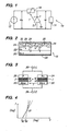
- Figure 1 is a schematic circuit diagram of a shunt-configured over-voltage protection circuit in which a PPTC element is thermally, as well as electrically, coupled to a reverse avalanche or Zener breakdown protection diode element in accordance with principles of the present invention.
- Figure 2 is an enlarged view in elevation and section of an improved energy-pulse-withstanding diode in accordance with principles of the present invention.
- Figure 3 is an enlarged diagrammatic sectional view and schematic circuit of two representative diode sections of the Figure 2 diode structure.
- Figure 4 is a graph (ordinate axis log scale) illustrating reverse breakdown IV characteristics of the Figure 3 model.
- Figure 5 is an enlarged diagrammatic top plan view of one preferred example of a semiconductor diode structure in accordance with the Figure 2 principles.
- Figure 6 is an enlarged diagrammatic top plan view of a second preferred example of a semiconductor diode structure in accordance with the Figure 2 principles.
- Figure 7 is a graph of output voltage versus time of a reverse bias over-voltage pulse applied to the Figure 1 protection circuit.
- Figure 7A is a graph of output voltage when a current-limited source applies the over-voltage pulse.
- Figure 8 is a graph of current versus time of the reverse bias over-voltage pulse of Figure 7.
- Figure 8A is a graph of current versus time of the reverse bias over-voltage pulse depicted in Figure 7A.
- Figure 9 is a graph of input voltage versus time of the Figure 7 reverse bias over-voltage pulse.
- Figure 9A is a graph of input voltage versus time of the reverse bias over-voltage pulse depicted in Figure 7A.
- Figures 10A, 10B, 10C, 10D and 11E present a sequence of processing steps for constructing a diode incorporating the Figure 2 principles of the present invention.
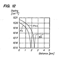
- Figures 11 and 12 present two examples of doping profile per cubic centimeter that are applicable to a diode made in accordance with the Figures 10A-10E process sequence.
- This diode includes higher resistivity regions (e.g. p+ regions) created through epitaxial growth or impurity diffusions. Heavier doping is provided in cell regions (e.g. p++) of the diode to insure Zener tunneling and/or impact ionization at a reverse bias voltage breakdown level. As the chip temperature increases, the less heavily doped (p+) regions reach intrinsic (ohmic) transition temperature before the more heavily doped (p++) cell regions, thus focusing anode-cathode current through these less heavily doped areas of the chip die.
- This transfer of current flow increases the temperature in the less heavily doped regions, thereby spreading the temperature more evenly across the chip die and affecting the ohmic current-voltage behavior of the less heavily doped regions.
- the ratio of intrinsic/Zener voltage levels will vary in accordance with doping concentrations, die layout of the regions and cells and temperature dissipation capabilities (heat sinking) of the diode die.
- FIG. 1 illustrates an exemplary shunt regulator circuit 10.
- the circuit 10 is connected electrically between an energy source 12 and a load 14; and, the circuit 10 includes a shunt regulator-protector diode element 16, such as a reverse biased avalanche breakdown diode or Zener diode in accordance with principles of the present invention.
- the circuit 10 also includes a series resistive element 18, most preferably a PPTC resistive element.
- the element 16 is most preferably thermally connected to the PPTC resistive element 18, for example, by having the die of element 16 in direct physical contact with the PPTC resistive element, as taught for example in commonly assigned U.S. Patent No. 6,518,731, referred to above, the disclosure thereof being incorporated herein by reference.
- overvoltage means that the voltage level of the energy pulse is above a reverse avalanche breakdown rating, or Zener tunneling rating, of the diode 16. This current flow results in a rapid heat build up within the diode 16. Because of the thermal coupling, the diode's heat is transferred to the PPTC element 18. After a short heating interval brought on by the energy pulse the PPTC element 18 will reach a "trip" temperature and thereupon rapidly increase in electrical resistance. When the PPTC element 18 enters its trip state the current flow through the regulator diode 16 and the load 14 is substantially reduced.
- thermal heating in response to the energy pulse is spread more uniformly throughout the structure of the diode 16 and allows it to absorb more energy and withstand greater heat over a longer initial heating interval without resultant irreversible damage or failure, than occurs in Zener diode devices of the prior art.
- FIG. 2 illustrates an exemplary structure forming the Zener diode 16 in accordance with principles of the present invention.
- the multi-layer diode 16 includes a semiconductor substrate 20 such as a highly doped n-carrier silicon wafer or chip.
- An epitaxial layer 22 of less heavily doped n-carrier silicon is formed on the substrate 20.
- At least one, and preferably a series of heavily doped p-carrier cells 24 are formed in the epitaxial layer 22 and extend into physical and electrical proximity of the highly doped n-carrier silicon substrate 20.
- Lightly doped p-carrier regions 26 extend between the heavily doped cells 24.
- While multiple cells 24 and regions 26 are shown in an interleaved arrangement in Figures 2, 5, and 6, a single cell 24 having a suitably sinuous, or other continuous, form and being distributed across a chip otherwise forming the region 26 is also within the scope of the present invention.
- the relative junction's doping depths into the epitaxial layer 22 which form cells 24 and regions 26 may vary, depending upon desired diode characteristics. As shown in Figures 2 and 12, the depth of heavily doped cells 24 is greater than the depth of interleaved less heavily doped regions 26, but the reverse arrangement is also within contemplation of the present invention as shown by the graph of doping concentrations in Figure 11, for example.
- a bottom metal electrode layer (anode) 28 is preferably formed to be coextensive with a lower major surface of the silicon substrate 20; and a top metal conductor layer (cathode) 30 is preferably formed to be coextensive with and electrically connected to an outer surface of the cells 24 and the regions 26.
- the chip substrate 20 is heavily doped negative carrier, n-type material on the order of at least 10 20 n-type dopant ions/cm 3 (N++).
- the epitaxial layer 22 is less heavily doped negative carrier N-type material on the order of about 10 17 dopant ions/cm 3 (N+).
- the heavily positive carrier p-doped cells 24 are in a range of 10 21 to 10 15 /cm 3 ; and, the more lightly doped positive carrier p-doped regions 26 on the order of 10 20 to 10 15 /cm 3 , as a function of distance as shown in Figures 11 and 12, for example.
- the heavily doped cells 24 ensure initial Zener tunneling (or reverse avalanche breakdown as the case may be) through each path from the p++ cell 24 to an adjacently underlying n++ region of the substrate as shown by arrows labeled "I" in Figure 2 shown extending from the cells 24.
- the more lightly doped regions 26 may reach a transition temperature at which silicon atoms forming the substrate and the epitaxial layer begin emitting electrons, increasing the leakage current and possibly reaching a level at which there is no energy or potential barrier between the p-region 26 and the n+ region 22 (herein referred to as an "intrinsic" or “ohmic” condition manifested by bi-directional low resistance, high current flow).
- an intrinsic, ohmic state which occurs at a lower substrate temperature than at the heavily doped p++ cells 24
- current flow through the Zener structure (and local heating) thereupon becomes distributed more evenly throughout the chip substrate.
- the lightly doped p+ regions 26 reach intrinsic (ohmic) high temperature, current flow becomes concentrated through these bi-directional ohmic regions as shown by the T arrow bisecting the regions 26 in Figure 2.
- the current flow through the ohmic regions may increase the temperature, thus affecting the ohmic-like I-V behavior.
- the ratio of intrinsic/Zener voltages of the diode 18 in response to an energy pulse will vary with doping, die layout and temperature/heatsinking of the diode device.
- Figure 3 symbolically divides the diode 16 into two diodes, one including the lightly doped region 26 (left diode) and the other including the heavily doped cell 24 (right diode). If these two diodes are reverse biased by applying a positive potential to electrode 28 and a negative return path at electrode 30, two depletion regions will be formed: a wider region A1 in the less heavily doped left diode and a narrower region A2 in the more heavily doped right diode. As the reverse bias voltage is increased a level is reached (V B2 in Figure 4) a first critical field is reached at which avalanche current or tunneling current will begin to flow in the right diode, but not in the left diode.
- the critical field will happen somewhere in the idealized right diode in the vicinity of its metallurgical junction (J). As the voltage increases, a second critical field is reached (voltage level V B1 in Figure 4) at which avalanche current or tunneling current will begin to flow in the left diode as well. A composite current flow through both diodes then results, beginning at an intercept point (IP) in the Figure 4 graph.
- the left diode is more lightly doped than the right diode, the left diode will reach a transition temperature (e.g. approximately 350°C) at which the left diode transitions to intrinsic or ohmic characteristics. This transition temperature is lower than a transition temperature of the more heavily doped right diode (e.g. 600°C to 700°C).
- a transition temperature of the more heavily doped right diode e.g. 600°C to 700°C.
- the diode 16 is better able to withstand a high energy pulse during a time interval sufficient to enable a coupled PPTC device to trip and place a very high electrical resistance in series between the current source 12 and the diode 16 (and load 14). As explained in connection with the Figure 1 example, survivability of the diode 16 is further enhanced when the diode 16 is effectively thermally coupled to the PPTC resistor device 18.
- Figure 5 shows an arrangement of the diode 16 wherein the highly doped cells 24 are defined in rows separated by rows of the lightly doped regions 26. In this example there are three discrete regions 26 separating four cells 24.
- Figure 6 shows an alternative arrangement of the diode 16 wherein there are, e.g., 16 highly doped generally square cells 24 separated by a continuous single lightly doped region 26. While square box cells 24 are illustrated by way of example, the cells could equally well be rounded or round cylinders, for example. Consequently, the cells and regions need not be geometric rectangular or square boxes, and they can follow a wide variety of other solid geometric shapes, whether straight-edged or having curved edges and/or being sinuous.
- Figure 7 illustrates a reverse bias overvoltage pulse Vr appearing across the shunt diode 16 and load 14 in the Figure 1 circuit.
- the levels Vzt1 and Vzm represent voltage levels across the anode and cathode electrodes of diode 16 at progressive time intervals during the pulse duration.
- Figure 8 graphs the current flowing through the diode 16
- Figure 9 graphs the input voltage supplied by energy pulse source 12.
- the diode temperature may increase to a level consistent with intrinsic doping conditions.
- the reverse blocking capabilities of the PN junction at region(s) 26 are significantly reduced or cease to exist, and the cathode-anode path will exhibit ohmic behavior.
- the electrical resistance of the PPTC element 18 will increase due to its intrinsic power dissipation and assisted heating from the die of diode 16. As the resistance of PPTC element 18 increases, the diode power dissipation decreases. At a time t2 later than time t1 the p-n junction regains most of its voltage blocking capabilities with the result that current flowing through the diode 16 decreases.
- FIGS 7A, 8A, and 9A respectively depict Vr, Iz and Vin waveforms when using a current-limited energy pulse source.
- the output voltage Vr ( Figure 7A) will fold back partially and recover after the PPTC element 18 "trips" to its very high resistance state at time t3, for example. While the current through the diode 16 remains constant ( Figure 8A), the input voltage will vary ( Figure 9A) between times t1 and t3.
- Figures 10A through 10E progressively illustrate at a simplified level a process sequence for making a high energy clamp diode, such as diode 16.
- Figure 10A shows a first series of process steps.
- An n-type, heavily doped silicon wafer 120 is subjected to epitaxial layer growth.
- An epitaxial n+ layer 122 is grown on the top surface of the n++ wafer 120.
- the n+ layer 122 has a doping concentration lower than the n++ wafer 120. While layer 122 is shown as a heavily doped n++, a heavily doped p++ wafer having a less heavily doped p+ epitaxial layer can be used as well.
- a layer 123 of silicon dioxide is grown on the top surface of the epitaxial layer 122.
- the thickness of epitaxial layer 122 can vary over a range; in the present example the epitaxial layer thickness is approximately 5 microns.
- the silicon dioxide layer 123 is approximately 1 micron thick.
- the starting wafer or substrate is preferably chosen to have the lowest possible resistivity (highest doping level), so that the wafer (chip) contribution to the diode's total parasitic series resistance is minimized. Therefore, the epitaxial layer should exhibit a lower doping level of the same type carrier, or have an opposite polarity carrier doping. If a higher series resistance is acceptable in a particular circuit protection application, doping levels can be traded off by using a substrate with a lower doping level and eliminating the top side epitaxial layer. This alternative approach would be expected to lower the manufacturing cost of the resultant protection diode.
- FIG. 10B shows a second series of process steps.
- An opening 125 is defined in the silicon dioxide layer 123, by use of conventional masking and etch techniques. This opening will have an area equal to an active area of each finished diode formed by and yielded from the processed wafer 120. In practice, the opening is in a range of 1 mm by 1 mm, but can be larger or smaller.
- a p-carrier ion implantation and a short diffusion are carried out, forming a layer 127. Any conventional doping technique can be used to create the p+ carrier layer 127 in the n+ epitaxial layer 122.
- Figure 10C shows a third series of process steps.
- a photoresist mask 129 is formed and patterned to define an array of openings 131 in the diode area 125 defined by the Figure 10B step.
- a p+ carrier ion implantation is carried out through the openings defined by the patterned photoresist mask 129.
- the implantation dosage is selected to create a doping level in newly doped regions 124 in excess of the doping level of region 127.
- Figure 10D shows a fourth series of process steps.
- the photoresist layer 129 is removed using conventional techniques and a diffusion step is carried out.
- the diffusion step forms the heavily doped cell regions 24 and the less heavily doped regions 26 of the diode 16.
- the p++ openings are typically approximately 15 microns wide, but other widths and lengths can be used, depending upon a particular diode design.
- Final junction depth of the cells 24 is approximately 2 microns.
- Figure 10E shows a final series of process steps. Top contact metallization is applied forming the cathode electrode 30, and bottom contact metallization is applied forming the anode electrode 28. The wafer is then "diced” in order to yield individual dies of diodes 16. The dies may be packaged as individual electrical components, or they may be combined directly with resistive elements, such as PPTC resistive element 18, as explained above.
- Figures 11 and 12 show two types of doping impurity distributions per cubic centimeter that may be used in making the exemplary diode 16.
- Figure 11 shows that the p++ concentration of cells 24 extends into the layer 22 for a distance less than the p+ layer of regions 26.
- Figure 12 shows the p++ concentration of cell 24 extends into the layer 22 for a distance greater than the p+ region 26, as shown diagrammatically in Figure 2.
- the doping values are shown as reference examples, and higher or lower values can be used, depending upon the intended application or available processing capabilities and conditions.
Landscapes
- Semiconductor Integrated Circuits (AREA)
- Metal-Oxide And Bipolar Metal-Oxide Semiconductor Integrated Circuits (AREA)
- Emergency Protection Circuit Devices (AREA)
Abstract
Description
Claims (17)
- A semiconductor device (16) consisting essentially of:(a) a planar substrate (20) of semiconductor material having carriers of a first type of conductivity in a first, high concentration level, a first major face and a second major face opposite to said first major face;(b) a layer (22) of semiconductor material being one of in or on said substrate (20) adjacent said first major face, having carriers of said first type of conductivity in a second concentration level lower than said first level, and having an outer surface;(c) at least one region (26) formed at said outer surface and having carriers of a second type of conductivity in a third concentration level;(d) at least one cell (24) formed at said outer surface and having carriers of said second type of conductivity in a fourth concentration level greater than said third concentration level;(e) a first electrode layer (30) formed at said outer surface; and(f) a second electrode layer (28) formed at said second major face.
- A semiconductor device (16) consisting essentially of:(a) a planar substrate (20) of semiconductor material having carriers of a first type of conductivity in a first predetermined concentration level, a first major face and a second major face opposite to said first major face;(b) at least one region (26) formed at said first major face and having carriers of a second type of conductivity in a second predetermined concentration level;(c) at least one cell (24) formed at said first major face and having carriers of said second type of conductivity in a second concentration level greater than said second concentration level;(d) a first electrode layer (30) formed at said first major face; and(e) a second electrode layer (28) formed at said second major face.
- The semiconductor device (16) set forth in claim 1 or 2 wherein said at least one region (26) extends to a first predetermined depth into said layer (22) and wherein said at least one cell (24) extends to a second predetermined depth into said layer (22).
- The semiconductor device (16) set forth in claim 3 wherein (a) said second predetermined depth is greater than said first predetermined depth, or (b) said second predetermined depth is less than or equal to said first predetermined depth.
- The semiconductor device (16) set forth in any preceding claim wherein said carriers of said first type of conductivity are n-carriers and wherein said carriers of said second type of conductivity are p-carriers.
- The semiconductor device set forth in any one of claims 1 to 4 wherein said carriers of said first type of conductivity are p-carriers and wherein said carriers of said second type of conductivity are n-carriers.
- The semiconductor device (16) set forth in any preceding claim wherein said device (16) comprises a plurality of cells (24) separated from each other by said region (26).
- The semiconductor device set forth in any one of claims 1 to 6 wherein said device comprises a plurality of cells and a plurality of regions, and wherein said plurality of cells are separated from each other by said plurality of regions.
- The semiconductor device set forth in any preceding claim wherein said layer comprises an epitaxial layer (22) formed on said substrate (20).
- A circuit (10) including the semiconductor device (16) set forth in any preceding claim wherein at least one of said electrodes (28, 30) of said device (16) is electrically connected to a circuit protection element (18), and said device (16) is in thermal contact with a circuit protection element (18).
- The circuit (10) as set forth in claim 10 wherein said circuit protection element (18) comprises a polymeric positive temperature coefficient (PPTC) resistive element.
- The circuit set forth in claim 11 wherein the semiconductor device (16) is connected in reverse bias voltage arrangement and constitutes a protection circuit operative to absorb an energy pulse having a voltage in excess of a predetermined reverse bias voltage level, convert said pulse to heat, and transfer said heat to said circuit protection element (18).
- A circuit (10) comprising the semiconductor device (16) set forth in claim 5 wherein said first electrode (30) forms a cathode connection and said second electrode (28) forms an anode connection, and further comprising a polymeric positive temperature coefficient (PPTC) resistive element (18) electrically connected in series with said cathode connection and thermally coupled to said device (16) by direct contact therewith.
- The circuit (10) set forth in claim (13) comprising an overvoltage protection circuit wherein the PPTC resistive element (18) is connected in series between a source (12) and a load (14), and wherein said semiconductor device (16) is connected in parallel across said load (14).
- The semiconductor device (16) set forth in claim 5 wherein the planar substrate (20) is a negative carrier, n-type doping material having approximately at least 1020 n-type dopant ions/cm3; wherein the epitaxial layer (22) is a negative carrier, n-type doping material having approximately 5x10¹⁷ dopant ions/cm3; the at least one region (26) is a positive carrier, p-type doping material having p-type dopants in a range between 1020 and 1015 dopant ions/cm3, and the at least one cell (24) is a positive carrier, p-type doping material having p-type dopants in a range between 5x10²¹ and 1015 dopant ions/cm3.
- A method for making a semiconductor device (16) comprising steps of:(a) forming a planar substrate (120) of semiconductor material having carriers of a first type of conductivity in a first, high concentration level, a first major face and a second major face opposite to said first major face;(b) forming an epitaxial layer (122) of semiconductor material on said first major face with carriers of said first type of conductivity in a second concentration level lower than said first level, and an outer surface;(c) forming at least one region (26) at said outer surface with carriers of a second type of conductivity in a third concentration level;(d) forming at least one cell (24) at said outer surface with carriers of said second type of conductivity in a fourth concentration level greater than said third concentration level;(e) forming a first electrode layer (30) at said outer surface; and(f) forming a second electrode layer (28) at said second major face.
- A method for making a semiconductor device comprising steps of:(a) forming a planar substrate of semiconductor material (120) having carriers of a first type of conductivity in a first predetermined concentration level, a first major face and a second major face opposite to said first major face;(b) forming at least one region (26) at said first major face with carriers of a second type of conductivity in a second predetermined concentration level;(c) forming at least one cell (24) at said first major face with carriers of said second type of conductivity in a second concentration level greater than said second concentration level;(d) forming a first electrode layer (30) formed at said first major face; and(e) forming a second electrode layer (28) formed at said second major face.
Applications Claiming Priority (2)
| Application Number | Priority Date | Filing Date | Title |
|---|---|---|---|
| US868583 | 2004-06-14 | ||
| US10/868,583 US20050275065A1 (en) | 2004-06-14 | 2004-06-14 | Diode with improved energy impulse rating |
Publications (2)
| Publication Number | Publication Date |
|---|---|
| EP1608025A2 true EP1608025A2 (en) | 2005-12-21 |
| EP1608025A3 EP1608025A3 (en) | 2006-04-12 |
Family
ID=34940152
Family Applications (1)
| Application Number | Title | Priority Date | Filing Date |
|---|---|---|---|
| EP05105161A Withdrawn EP1608025A3 (en) | 2004-06-14 | 2005-06-13 | Overvoltage protection diode |
Country Status (6)
| Country | Link |
|---|---|
| US (2) | US20050275065A1 (en) |
| EP (1) | EP1608025A3 (en) |
| JP (1) | JP2006032923A (en) |
| KR (1) | KR20060049581A (en) |
| CN (1) | CN1722470A (en) |
| TW (1) | TW200616301A (en) |
Cited By (1)
| Publication number | Priority date | Publication date | Assignee | Title |
|---|---|---|---|---|
| DE102007024461A1 (en) * | 2007-05-25 | 2008-11-27 | Infineon Technologies Austria Ag | Semiconductor element |
Families Citing this family (30)
| Publication number | Priority date | Publication date | Assignee | Title |
|---|---|---|---|---|
| US8525222B2 (en) | 2005-03-25 | 2013-09-03 | Vishay General Semiconductor Llc | Process for forming a planar diode using one mask |
| CN100428472C (en) * | 2005-08-24 | 2008-10-22 | 中芯国际集成电路制造(上海)有限公司 | Low voltage trigger and storage area electrostatic discharge device |
| US7619262B2 (en) * | 2006-11-16 | 2009-11-17 | Delphi Technologies, Inc. | Method and device for electrostatic discharge protection |
| US8304785B2 (en) * | 2008-07-29 | 2012-11-06 | Industrial Technology Research Institute | LED structure, manufacturing method thereof and LED module |
| US8213134B2 (en) * | 2008-12-30 | 2012-07-03 | International Business Machines Corporation | Apparatus, system, and method to prevent smoke in a power supply powered by a current limited source |
| US9019674B2 (en) | 2010-11-23 | 2015-04-28 | Fairchild Semiconductor Corporation | Input power port protection component |
| US8861164B2 (en) | 2011-02-04 | 2014-10-14 | Fairchild Semiconductor Corporation | Integrated overdrive and overvoltage protection device |
| US9379257B2 (en) | 2012-06-22 | 2016-06-28 | Infineon Technologies Ag | Electrical device and method for manufacturing same |
| US20140191319A1 (en) * | 2013-01-04 | 2014-07-10 | GlobalFoundries, Inc. | Finfet compatible diode for esd protection |
| US9112346B2 (en) | 2013-03-14 | 2015-08-18 | Fairchild Semiconductor Corporation | Input power protection |
| US9172239B2 (en) | 2013-03-15 | 2015-10-27 | Fairchild Semiconductor Corporation | Methods and apparatus related to a precision input power protection device |
| JPWO2014162987A1 (en) * | 2013-04-04 | 2017-02-16 | ローム株式会社 | Composite chip parts, circuit assemblies and electronics |
| US9508841B2 (en) * | 2013-08-01 | 2016-11-29 | General Electric Company | Method and system for a semiconductor device with integrated transient voltage suppression |
| KR101414005B1 (en) * | 2013-10-31 | 2014-07-04 | 주식회사 케이이씨 | Transient voltage suppressor and its manufacturing method |
| US9472570B2 (en) * | 2014-02-18 | 2016-10-18 | Globalfoundries Inc. | Diode biased body contacted transistor |
| US9093568B1 (en) * | 2014-04-16 | 2015-07-28 | Infineon Technologies Ag | Semiconductor diode |
| US9735147B2 (en) | 2014-09-15 | 2017-08-15 | Fairchild Semiconductor Corporation | Fast and stable ultra low drop-out (LDO) voltage clamp device |
| DE102015108091A1 (en) * | 2015-05-21 | 2016-11-24 | Infineon Technologies Dresden Gmbh | Transistor arrangement with power transistors and voltage-limiting components |
| US12074225B2 (en) | 2018-12-03 | 2024-08-27 | Macom Technology Solutions Holdings, Inc. | PIN diodes with multi-thickness intrinsic regions |
| CN109888024B (en) * | 2018-12-29 | 2024-04-02 | 厦门芯光润泽科技有限公司 | MPS diode device and preparation method thereof |
| CN109860273B (en) * | 2018-12-29 | 2024-04-02 | 厦门芯光润泽科技有限公司 | MPS diode device and preparation method thereof |
| CN113424317A (en) | 2019-02-12 | 2021-09-21 | 镁可微波技术有限公司 | Monolithic multi-I-region diode limiter |
| EP3931964B1 (en) | 2019-02-28 | 2024-12-04 | MACOM Technology Solutions Holdings, Inc. | Monolithic multi-i region diode switches |
| FR3093598B1 (en) * | 2019-03-05 | 2023-08-04 | St Microelectronics Srl | Surge protection device |
| CN111128698A (en) * | 2019-12-26 | 2020-05-08 | 安徽芯旭半导体有限公司 | Novel diffusion process of TVS chip |
| US10931099B1 (en) | 2020-02-26 | 2021-02-23 | Calamp Corp. | Systems and methods for automatic threshold sensing for UVLO circuits in a multi-battery environment |
| EP4111567A4 (en) * | 2020-02-26 | 2023-11-29 | Calamp Corp. | SYSTEMS AND METHODS FOR AUTOMATIC THRESHOLD DETECTION FOR UVLO CIRCUITS IN A MULTI-BATTERY ENVIRONMENT |
| US20210343837A1 (en) * | 2020-05-01 | 2021-11-04 | Vanguard International Semiconductor Corporation | Semiconductor structures |
| US11570852B2 (en) * | 2020-10-15 | 2023-01-31 | Littelfuse, Inc. | PPTC heating element having varying power density |
| US11600730B2 (en) * | 2020-12-03 | 2023-03-07 | Micross Corpus Christi Corporation | Spiral transient voltage suppressor or Zener structure |
Family Cites Families (25)
| Publication number | Priority date | Publication date | Assignee | Title |
|---|---|---|---|---|
| US3391287A (en) * | 1965-07-30 | 1968-07-02 | Westinghouse Electric Corp | Guard junctions for p-nu junction semiconductor devices |
| FR1583248A (en) * | 1968-06-27 | 1969-10-24 | ||
| US4030117A (en) * | 1975-03-10 | 1977-06-14 | International Telephone And Telegraph Corporation | Zener diode |
| US4099998A (en) * | 1975-11-03 | 1978-07-11 | General Electric Company | Method of making zener diodes with selectively variable breakdown voltages |
| FR2454704A1 (en) * | 1979-04-20 | 1980-11-14 | Thomson Csf | PLANAR AVALANCHE DIODE WITH BREAKDOWN VOLTAGE BETWEEN 4 AND 8 VOLTS |
| GB2050694B (en) * | 1979-05-07 | 1983-09-28 | Nippon Telegraph & Telephone | Electrode structure for a semiconductor device |
| JPS59143370A (en) | 1983-02-04 | 1984-08-16 | Hitachi Ltd | Semiconductor rectifying device |
| JPS6136979A (en) | 1984-07-30 | 1986-02-21 | Nec Corp | Constant-voltage diode |
| DE3621200A1 (en) | 1986-06-25 | 1988-01-07 | Siemens Ag | PROTECTIVE BLOCK FOR TELECOMMUNICATION SYSTEMS |
| GB8713440D0 (en) * | 1987-06-09 | 1987-07-15 | Texas Instruments Ltd | Semiconductor device |
| US4901183A (en) * | 1988-08-29 | 1990-02-13 | World Products, Inc. | Surge protection device |
| JP2570022B2 (en) * | 1991-09-20 | 1997-01-08 | 株式会社日立製作所 | Constant voltage diode, power conversion device using the same, and method of manufacturing constant voltage diode |
| DE4405815A1 (en) * | 1993-02-24 | 1994-08-25 | Samsung Electronics Co Ltd | Semiconductor device having an anode layer which has low-concentration regions formed by selective diffusion |
| JP2666743B2 (en) * | 1994-11-22 | 1997-10-22 | 日本電気株式会社 | Constant voltage diode |
| US6215633B1 (en) * | 1996-02-26 | 2001-04-10 | Marconi Communications, Inc. | Active current limiter |
| US5851882A (en) * | 1996-05-06 | 1998-12-22 | Micron Technology, Inc. | ZPROM manufacture and design and methods for forming thin structures using spacers as an etching mask |
| JP3287269B2 (en) * | 1997-06-02 | 2002-06-04 | 富士電機株式会社 | Diode and manufacturing method thereof |
| DE19723176C1 (en) * | 1997-06-03 | 1998-08-27 | Daimler Benz Ag | Semiconductor device with alternate p-n and Schottky junctions |
| JP3191747B2 (en) * | 1997-11-13 | 2001-07-23 | 富士電機株式会社 | MOS type semiconductor device |
| WO1999038205A1 (en) * | 1998-01-21 | 1999-07-29 | Robert Bosch Gmbh | Method for producing diodes |
| US6331763B1 (en) * | 1998-04-15 | 2001-12-18 | Tyco Electronics Corporation | Devices and methods for protection of rechargeable elements |
| US6628498B2 (en) * | 2000-08-28 | 2003-09-30 | Steven J. Whitney | Integrated electrostatic discharge and overcurrent device |
| GB0108792D0 (en) * | 2001-04-07 | 2001-05-30 | Power Innovations Ltd | Overvoltage protection device |
| EP1396030B1 (en) * | 2001-04-11 | 2011-06-29 | Silicon Semiconductor Corporation | Vertical power semiconductor device and method of making the same |
| US7369387B2 (en) * | 2004-11-09 | 2008-05-06 | Fultec Semiconductor, Inc. | Apparatus and method for temperature-dependent transient blocking |
-
2004
- 2004-06-14 US US10/868,583 patent/US20050275065A1/en not_active Abandoned
-
2005
- 2005-06-13 EP EP05105161A patent/EP1608025A3/en not_active Withdrawn
- 2005-06-13 TW TW094119428A patent/TW200616301A/en unknown
- 2005-06-13 KR KR1020050050318A patent/KR20060049581A/en not_active Abandoned
- 2005-06-13 JP JP2005172106A patent/JP2006032923A/en active Pending
- 2005-06-14 CN CNA2005100837996A patent/CN1722470A/en active Pending
-
2007
- 2007-03-15 US US11/724,907 patent/US7932133B2/en not_active Expired - Lifetime
Cited By (3)
| Publication number | Priority date | Publication date | Assignee | Title |
|---|---|---|---|---|
| DE102007024461A1 (en) * | 2007-05-25 | 2008-11-27 | Infineon Technologies Austria Ag | Semiconductor element |
| US8035195B2 (en) | 2007-05-25 | 2011-10-11 | Infineon Technologies Ag | Semiconductor element |
| DE102007024461B4 (en) * | 2007-05-25 | 2012-10-11 | Infineon Technologies Austria Ag | Semiconductor element and method for its production |
Also Published As
| Publication number | Publication date |
|---|---|
| JP2006032923A (en) | 2006-02-02 |
| CN1722470A (en) | 2006-01-18 |
| US7932133B2 (en) | 2011-04-26 |
| TW200616301A (en) | 2006-05-16 |
| US20050275065A1 (en) | 2005-12-15 |
| EP1608025A3 (en) | 2006-04-12 |
| KR20060049581A (en) | 2006-05-19 |
| US20070166942A1 (en) | 2007-07-19 |
Similar Documents
| Publication | Publication Date | Title |
|---|---|---|
| US7932133B2 (en) | Circuit protection method using diode with improved energy impulse rating | |
| JP2006032923A5 (en) | ||
| TWI405323B (en) | Non-blocking vertical transient voltage suppression diode array structure using trench isolation and manufacturing method thereof | |
| US9064923B2 (en) | Bipolar semiconductor component with a fully depletable channel zone | |
| US20080044955A1 (en) | Electrostatic discharge protection device for digital circuits and for applications with input/output bipolar voltage much higher than the core circuit power supply | |
| US20060220138A1 (en) | ESD protection circuit with scalable current capacity and voltage capacity | |
| JP5784773B2 (en) | Schottky diode with integrated PN junction | |
| CN104752417A (en) | Silicon controlled rectifier protection device and forming method thereof | |
| TW201705498A (en) | Bidirectional through semiconductor device and method of fabricating the same | |
| CN113646901A (en) | Schottky rectifier with surge current stability and method of making the same | |
| US9991173B2 (en) | Bidirectional semiconductor device for protection against electrostatic discharges | |
| US6232625B1 (en) | Semiconductor configuration and use thereof | |
| EP0978145B1 (en) | Semi-conductor device and use thereof | |
| KR20240078639A (en) | Structure and method for sic based protection device | |
| SE455552B (en) | SEMICONDUCTOR DEVICE INCLUDING AN OVERVOLTAGE CIRCUIT | |
| JP3131823B2 (en) | Multi-terminal surge protection device | |
| US6768176B1 (en) | Electrostatic discharge protection circuit | |
| US7238553B1 (en) | Method of forming a high-voltage silicon controlled rectifier structure with improved punch through resistance | |
| KR101800331B1 (en) | Zener diode having a polysilicon layer for improved reverse surge capability and decreased leakage current | |
| US20030213996A1 (en) | Integrated circuit provided with overvoltage protection and method for manufacture thereof | |
| US20140367829A1 (en) | ESD Protection Apparatus | |
| CN112420691A (en) | Distributed ESD device with embedded SCR structure | |
| KR20090113964A (en) | Manufacturing method of high voltage schottky barrier diode | |
| CN222356849U (en) | Electrostatic protection device | |
| JPS5931869B2 (en) | Electrostatic induction thyristor |
Legal Events
| Date | Code | Title | Description |
|---|---|---|---|
| PUAI | Public reference made under article 153(3) epc to a published international application that has entered the european phase |
Free format text: ORIGINAL CODE: 0009012 |
|
| AK | Designated contracting states |
Kind code of ref document: A2 Designated state(s): AT BE BG CH CY CZ DE DK EE ES FI FR GB GR HU IE IS IT LI LT LU MC NL PL PT RO SE SI SK TR |
|
| AX | Request for extension of the european patent |
Extension state: AL BA HR LV MK YU |
|
| PUAL | Search report despatched |
Free format text: ORIGINAL CODE: 0009013 |
|
| AK | Designated contracting states |
Kind code of ref document: A3 Designated state(s): AT BE BG CH CY CZ DE DK EE ES FI FR GB GR HU IE IS IT LI LT LU MC NL PL PT RO SE SI SK TR |
|
| AX | Request for extension of the european patent |
Extension state: AL BA HR LV MK YU |
|
| 17P | Request for examination filed |
Effective date: 20060922 |
|
| AKX | Designation fees paid |
Designated state(s): DE FR GB |
|
| 17Q | First examination report despatched |
Effective date: 20071114 |
|
| STAA | Information on the status of an ep patent application or granted ep patent |
Free format text: STATUS: THE APPLICATION IS DEEMED TO BE WITHDRAWN |
|
| 18D | Application deemed to be withdrawn |
Effective date: 20080527 |