EP1608015A2 - Semiconductor device capsule - Google Patents
Semiconductor device capsule Download PDFInfo
- Publication number
- EP1608015A2 EP1608015A2 EP05105022A EP05105022A EP1608015A2 EP 1608015 A2 EP1608015 A2 EP 1608015A2 EP 05105022 A EP05105022 A EP 05105022A EP 05105022 A EP05105022 A EP 05105022A EP 1608015 A2 EP1608015 A2 EP 1608015A2
- Authority
- EP
- European Patent Office
- Prior art keywords
- semiconductor device
- chips
- pole
- poles
- device capsule
- Prior art date
- Legal status (The legal status is an assumption and is not a legal conclusion. Google has not performed a legal analysis and makes no representation as to the accuracy of the status listed.)
- Ceased
Links
Images


Classifications
-
- H—ELECTRICITY
- H10—SEMICONDUCTOR DEVICES; ELECTRIC SOLID-STATE DEVICES NOT OTHERWISE PROVIDED FOR
- H10W—GENERIC PACKAGES, INTERCONNECTIONS, CONNECTORS OR OTHER CONSTRUCTIONAL DETAILS OF DEVICES COVERED BY CLASS H10
- H10W72/00—Interconnections or connectors in packages
-
- H—ELECTRICITY
- H10—SEMICONDUCTOR DEVICES; ELECTRIC SOLID-STATE DEVICES NOT OTHERWISE PROVIDED FOR
- H10W—GENERIC PACKAGES, INTERCONNECTIONS, CONNECTORS OR OTHER CONSTRUCTIONAL DETAILS OF DEVICES COVERED BY CLASS H10
- H10W90/00—Package configurations
Definitions
- the present invention relates to a semiconductor device capsule and, in particular, a multi-chip pressure contact semiconductor device capsule.
- Pressure-contact semiconductor device capsules 10 are often used in electricity transmission and distribution infrastructures, and typically include a semiconductor assembly 12 mounted between two opposed poles 14,16, as shown in Figure 1.
- the semiconductor assembly 12 and poles 14,16 are usually provided within an insulating (e.g. ceramic) enclosure (not shown).
- the capsule 10 is subject to a compressive mechanical clamping force to ensure good thermal, electrical and mechanical contact between the semiconductor assembly 12 and the poles 14,16.
- This force is usually applied through heat sinks 18,20 and/or solid surface plates placed either side of the capsule 10.
- the semiconductor assembly 12 During operation, the semiconductor assembly 12 generates heat, thereby heating the lower surface of the top pole 14 and the upper surface of the bottom pole 16. The upper surface of the top pole 14 and the lower surface of the bottom pole 16 are cooled by the heat sinks 18,20. This creates a thermal gradient and, as a result, causes the top and bottom poles 14,16, and other parts of the assembly, to bend in opposite directions, as illustrated in Figure 2.
- the metallization of the semiconductor wafer is conformable and is usually of sufficient thickness to compensate for the effects of bending.
- Contact between the wafer and the poles may be improved by interposing molybdenum or tungsten plates of intermediate expansion coefficient.
- the provision of molybdenum or tungsten plates also lessens the likelihood of the wafer cracking.
- the semiconductor assembly includes a multiplicity of separate chips
- bending results in poor distribution of thermal, electrical and mechanical contact, particularly near the circumference of the capsule.
- This causes poor equality of contact between the constituent chips, and results in electrical duty being concentrated on the chips located at the centre of the capsule.
- the chips located at the centre of the capsule may therefore overheat and fail.
- each of the chips and the poles may be improved by locating a spring on one side of each of the chips to provide a spring bias.
- Contact between each of the chips and the poles may also be improved by increasing the compressive mechanical clamping force in order to press flat the distortion caused by the thermo-mechanical bending of each pole.
- the magnitude of the compressive mechanical clamping force is limited since it is important not to damage the semiconductor chips. If the clamping force exceeds a predetermined value, the structure of the semiconductor chips will be damaged.
- An aim of the invention is to provide a pressure-contact semiconductor device capsule where equality of contact between the or each chip or group of chips within the semiconductor assembly and the poles is maintained during use throughout the whole temperature range permitted by the electrical properties of the semiconductor.
- a semiconductor device capsule comprising a semiconductor assembly mounted between opposed poles wherein at least one of the poles includes slots around the locality of the or each chip or group of chips within the semiconductor assembly to define a contact body portion on which the or each chip or group of chips is mounted and reduce the thickness of a laterally continuous body portion of the pole.
- a pressure-contact semiconductor device capsule 30 according to an embodiment of the invention is shown in Figure 3.
- the semiconductor device capsule 30 includes a semiconductor assembly 32 located between opposing top and bottom poles 34,36.
- the semiconductor assembly 32 and poles 34,36 are preferably located within an insulating (e.g. ceramic) enclosure (not shown).
- Each of the poles 34,36 is preferably a solid member formed from copper having an overall depth of approximately 10mm or greater.
- Slots 38 are formed in an upper surface 40 of the bottom pole 36 around the circumference of the or each chip or group of chips 46 within the semiconductor assembly 32.
- Each slot 38 extends part-way through the solid pole 36 to form a contact body portion 37 on which the or each chip or group of chips 46 is mounted. Since the slots 38 do not extend through the entire depth of the pole 36, a laterally continuous portion 39 of the pole 36 is retained beneath the contact body portion 37, the laterally continuous portion 39 of the pole 36 having a thickness D ( Figure 5).
- the depth of the slots 38 is preferably chosen such that the thickness D of the laterally continuous portion 39 is preferably approximately 3mm.
- the capsule 30 is subject to a compressive mechanical clamping force to ensure good thermal, electrical and mechanical contact between the semiconductor assembly 32 and each of the poles 34,36.
- This force is preferably applied through heat sinks 42,44 placed either side of the capsule 30.
- the semiconductor assembly 32 includes a plurality of semiconductor chips 46.
- the chips 46 are preferably arranged on the upper surface 40 of the bottom pole 36 in a grid-like or orthogonal pattern, one such arrangement being shown in Figure 4.
- the slots 38 are preferably arranged to extend across the upper surface 40 of the bottom pole 36 so as to form the intervening lines of a grid and define a plurality of contact body portions 37 on which the semiconductor chips 46 are mounted.
- an intermediate expansion coefficient such as, for example, molybdenum or tungsten
- the periphery 52 of the top face 54 of each of the semiconductor chips 46 may be required for edge passivation to preserve the voltage withstand at the chip edge. This means that the top face 54 of each of the semiconductor chips 46 may have a smaller contact area than the bottom face 50.
- the top pole 34 preferably includes a plurality of pillars 56 protruding from a lower surface 58 thereof. The pillars 56 correspond in number and position to the chips 46 located between the top and bottom poles 34,36.
- each of the pillars 56 is preferably about 3mm to 10mm. This height is sufficient to accommodate the chip passivation without increasing unduly the thermal resistance of the top pole 34.
- a further expansion matching plate 60 formed from a material having an intermediate expansion coefficient, such as, for example, molybdenum or tungsten, is interposed between the top face 54 of each of the chips 46 and a respective pillar 56, as shown in Figure 5.
- an intermediate expansion coefficient such as, for example, molybdenum or tungsten
- slots 62 are formed in the lower surface 58 of the top pole 34 about the circumference of each of the semiconductor chips 46.
- Each slot 62 extends part-way through the solid pole 34 to form contact body portions 61 on which the semiconductor chips 46 are mounted. Since the slots 62 do not extend through the entire depth of the pole 34, a laterally continuous portion 63 of the pole 34 is retained beneath the contact body portions 61, the laterally continuous portion 63 of the pole 34 having a thickness d ( Figure 5).
- the depth of the slots 62 is preferably chosen such that the thickness d of the laterally continuous portion 63 is preferably approximately 3mm.
- slots may be formed on only one of the poles 34,36.
- the depths of the slots in the top and/or bottom pole 34,36 and the thicknesses of the laterally continuous portions of the poles 63,39 may be varied depending on the expected generation of heat flux from the semiconductor assembly 32.
- each of the slots 38,62 formed in the top and bottom poles 34,36 is at least 1mm, and is preferably several millimetres.
- the provision of slots 38 which are several millimetres wide in the bottom pole 36 allows chip-locator members 64 to be inserted at one end into the slots 38, as shown in Figure 5.
- Each of the chip-locators 64 is preferably shaped to correspond to the shape of the intervening space between the poles 34,36 so that the other end of the chip-locator protrudes into the space separating adjacent pillars of the top pole 34.
- chip-locator members 64 assists in maintaining the relative positions of the individual components associated with each chip 46.
- chip location may be achieved by means of a continuous plate having apertures therein.
- the plate may be lain over the poles so that the poles extend through respective apertures.
- the compressive mechanical clamping force preferably applied through the heat sinks 42,44, maintains the chips 46, expansion matching plates 48,60, bottom pole 36 and pillars 56 in contact with each other. This contact may be enhanced by bonding each of the chips 46 to one or both of the expansion matching plates 48,60.
- the expansion matching plates 48,60 are preferably in sliding contact with the bottom pole 36 and pillars 56 respectively so as to allow relative movement therebetween.
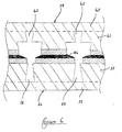
- the electrical behaviour of the semiconductor chips 46 in use generates heat. This heat is transferred to the lower surface 58 of the top pole 34 and the upper surface 40 of the bottom pole 36. The upper surface 66 of the top pole 34 and the lower surface 68 of the bottom pole 36 are cooled by the heat sinks 42,44. This creates a thermal gradient across the capsule 30.
- the thermal gradient means that the amount of thermal expansion of each of the contact body portions 37,61 reduces with distance from the chips, as shown in Figure 6.
- the provision of the slots 38,62 means that bending of the laterally continuous portions 39,63 is minimized.
- the provision of the slots 38,62 also reduces the lateral rigidity of each of the poles 34,36 by reducing the thickness d,D of the laterally continuous portions 63,39 of the poles 34,36, whilst maintaining the axial rigidity. It therefore reduces the size of the clamping force required to press the poles 34,36 flat.
- the thickness of the laterally continuous portions 63,39 of the poles 34,36 is typically 3mm.
- a substantially greater thickness than this, e.g. 5mm, would lead to greater thermo-mechanical distortion at elevated temperatures. This is unacceptable because it results in poor distribution of contact between the multiplicity of chips in a large multi-chip capsule with typically 125mm diameter poles.
- a substantially reduced thickness, e.g. less than 1mm, could result in shortening of the capsule life due to fatigue stress.
- the slots 38,62 have negligible effect on the electrical and thermal behaviour of the capsule 30 because the main current and heat flows are vertical, and the slots 38,62 only obstruct horizontal flows.
- the remaining laterally continuous portions 63,39 of each pole 34,36 is adequate to cope with any horizontal flows there are.
- Reducing the effect of the thermal gradient created across the capsule 30 during use means that it is possible to introduce a range of high power semiconductor devices based on silicon carbide technology using large-diameter, multi-chip capsules, which give the highest ratings possible.
- Such devices may contain typically 30 chips, each having an active surface area of 100mm 2 , or a higher number of chips having a smaller surface area (or a smaller number of chips having a larger surface area when the development of silicon carbide wafer material permits).
- the practical size of the device may be limited to 50mm pole diameter for the same heat flux per chip, which would accommodate only 4 such chips, so necessitating the connecting of approximately 7 such capsules in parallel to achieve the same power rating.
Landscapes
- Cooling Or The Like Of Semiconductors Or Solid State Devices (AREA)
- Lead Frames For Integrated Circuits (AREA)
- Die Bonding (AREA)
Abstract
Description
Claims (11)
- A semiconductor device capsule comprising a pair of opposed poles, each pole including a plurality of slots arranged to define respective contact body portions opposite one another and corresponding to a respective chip or group of chips, each contact body portion having a discrete expansion matching plate of intermediate expansion coefficient lying adjacent thereto, corresponding expansion matching plates having a respective chip or group of chips sandwiched therebetween, the slots reducing the thickness of a laterally continuous body portion of each pole, whereby the degree of flexure of the poles under a given clamping force is increased so as to maintain adequate thermal and electrical contact to each chip or group of chips within the capsule.
- A semiconductor device capsule according to Claim 1 wherein each of the poles is a solid member formed from copper.
- A semiconductor device capsule according to Claim 1 or Claim 2 wherein each pole has a depth of 10mm.
- A semiconductor device capsule according to any preceding claim wherein the slots around the locality of each chip or group of chips reduce the thickness of the laterally continuous portion of each pole to 3mm.
- A semiconductor device capsule according to any preceding claim wherein the semiconductor assembly includes a plurality of semiconductor chips arranged in a grid-like pattern.
- A semiconductor device capsule according to Claim 5 wherein the slots around the locality of each chip or group of chips are arranged so as to form the intervening lines of the grid and define a plurality of contact body portions on which the chips are mounted.
- A semiconductor device capsule according to any preceding claim wherein each expansion matching plate is formed from molybdenum or tungsten.
- A semiconductor device capsule according to any preceding claim wherein one of the poles includes one or more pillars protruding from its inner surface between the inner surface of the pole and respective expansion matching plates lying adjacent thereto.
- A semiconductor device capsule according to Claim 10 wherein the or each pillar has a height of 3mm to 10mm.
- A semiconductor device capsule according to any preceding claim further including one or more locator members received at each end in a slot formed in each pole so as to extend between the poles.
- A semiconductor device capsule generally as herein described with reference to and/or as illustrated in Figures 3-5 of the accompanying drawings.
Applications Claiming Priority (2)
| Application Number | Priority Date | Filing Date | Title |
|---|---|---|---|
| GB0412778 | 2004-06-09 | ||
| GB0412778A GB2425883B (en) | 2004-06-09 | 2004-06-09 | Semiconductor device capsule |
Publications (2)
| Publication Number | Publication Date |
|---|---|
| EP1608015A2 true EP1608015A2 (en) | 2005-12-21 |
| EP1608015A3 EP1608015A3 (en) | 2010-01-13 |
Family
ID=32696859
Family Applications (1)
| Application Number | Title | Priority Date | Filing Date |
|---|---|---|---|
| EP05105022A Ceased EP1608015A3 (en) | 2004-06-09 | 2005-06-08 | Semiconductor device capsule |
Country Status (3)
| Country | Link |
|---|---|
| US (1) | US7285852B2 (en) |
| EP (1) | EP1608015A3 (en) |
| GB (1) | GB2425883B (en) |
Cited By (1)
| Publication number | Priority date | Publication date | Assignee | Title |
|---|---|---|---|---|
| DE102013216709A1 (en) * | 2013-08-22 | 2015-02-26 | Infineon Technologies Ag | SEMICONDUCTOR ARRANGEMENT, METHOD FOR PRODUCING A NUMBER OF CHIP ASSEMBLIES AND METHOD FOR PRODUCING A SEMICONDUCTOR ASSEMBLY |
Families Citing this family (1)
| Publication number | Priority date | Publication date | Assignee | Title |
|---|---|---|---|---|
| DE102006010728A1 (en) * | 2005-12-05 | 2007-06-06 | Osram Opto Semiconductors Gmbh | Semiconductor component and laser device |
Family Cites Families (6)
| Publication number | Priority date | Publication date | Assignee | Title |
|---|---|---|---|---|
| JP3588503B2 (en) * | 1995-06-20 | 2004-11-10 | 株式会社東芝 | Pressure welding type semiconductor device |
| JPH09275186A (en) * | 1996-04-02 | 1997-10-21 | Fuji Electric Co Ltd | Semiconductor device |
| US5981310A (en) * | 1998-01-22 | 1999-11-09 | International Business Machines Corporation | Multi-chip heat-sink cap assembly |
| US6552264B2 (en) * | 1998-03-11 | 2003-04-22 | International Business Machines Corporation | High performance chip packaging and method |
| US6490161B1 (en) * | 2002-01-08 | 2002-12-03 | International Business Machines Corporation | Peripheral land grid array package with improved thermal performance |
| JP2004023083A (en) * | 2002-06-20 | 2004-01-22 | Toshiba Corp | Pressure welding type semiconductor device |
-
2004
- 2004-06-09 GB GB0412778A patent/GB2425883B/en not_active Expired - Fee Related
-
2005
- 2005-06-08 EP EP05105022A patent/EP1608015A3/en not_active Ceased
- 2005-06-09 US US11/149,573 patent/US7285852B2/en not_active Expired - Fee Related
Cited By (4)
| Publication number | Priority date | Publication date | Assignee | Title |
|---|---|---|---|---|
| DE102013216709A1 (en) * | 2013-08-22 | 2015-02-26 | Infineon Technologies Ag | SEMICONDUCTOR ARRANGEMENT, METHOD FOR PRODUCING A NUMBER OF CHIP ASSEMBLIES AND METHOD FOR PRODUCING A SEMICONDUCTOR ASSEMBLY |
| US9589859B2 (en) | 2013-08-22 | 2017-03-07 | Infineon Technologies Ag | Semiconductor arrangement, method for producing a number of chip assemblies and method for producing a semiconductor arrangement |
| US9984928B2 (en) | 2013-08-22 | 2018-05-29 | Infineon Technologies Ag | Method for producing a number of chip assemblies and method for producing a semiconductor arrangement |
| DE102013216709B4 (en) * | 2013-08-22 | 2021-03-25 | Infineon Technologies Ag | SEMICONDUCTOR ARRANGEMENT, METHOD FOR MANUFACTURING A NUMBER OF CHIP ASSEMBLIES AND METHOD FOR MANUFACTURING A SEMICONDUCTOR ARRANGEMENT |
Also Published As
| Publication number | Publication date |
|---|---|
| US7285852B2 (en) | 2007-10-23 |
| GB0412778D0 (en) | 2004-07-07 |
| EP1608015A3 (en) | 2010-01-13 |
| GB2425883A (en) | 2006-11-08 |
| US20060087027A1 (en) | 2006-04-27 |
| GB2425883B (en) | 2009-04-22 |
Similar Documents
| Publication | Publication Date | Title |
|---|---|---|
| CN107851643B (en) | Semiconductor device subassembly | |
| US6815814B2 (en) | Thermoelectric module | |
| US9179578B2 (en) | Semiconductor module and heat radiation member | |
| US8053830B2 (en) | Semiconductor device | |
| US9000580B2 (en) | Power semiconductor module with pressed baseplate and method for producing a power semiconductor module with pressed baseplate | |
| US9390995B2 (en) | Semiconductor device and method of manufacturing the same | |
| KR102562059B1 (en) | Thermally insulated electrical contact probe and heated platen assembly | |
| US8395262B2 (en) | Semiconductor device and method for manufacturing the same | |
| JP4069070B2 (en) | Power semiconductor module | |
| JP2002198477A (en) | Semiconductor device | |
| EP1376690B1 (en) | Pressure-contact type semiconductor device | |
| EP1608015A2 (en) | Semiconductor device capsule | |
| EP2560203A1 (en) | Power semiconductor arrangement | |
| US11574894B2 (en) | Semiconductor device sub-assembly | |
| CN110581384A (en) | Thermal insulation electric contact probe | |
| KR101830509B1 (en) | A heat sink for cooling chip and pattern and a circuit board using the same | |
| JPH09326448A (en) | Semiconductor device |
Legal Events
| Date | Code | Title | Description |
|---|---|---|---|
| PUAI | Public reference made under article 153(3) epc to a published international application that has entered the european phase |
Free format text: ORIGINAL CODE: 0009012 |
|
| AK | Designated contracting states |
Kind code of ref document: A2 Designated state(s): AT BE BG CH CY CZ DE DK EE ES FI FR GB GR HU IE IS IT LI LT LU MC NL PL PT RO SE SI SK TR |
|
| AX | Request for extension of the european patent |
Extension state: AL BA HR LV MK YU |
|
| RAP1 | Party data changed (applicant data changed or rights of an application transferred) |
Owner name: AREVA T&D SAS |
|
| RAP1 | Party data changed (applicant data changed or rights of an application transferred) |
Owner name: AREVA T&D SAS |
|
| PUAL | Search report despatched |
Free format text: ORIGINAL CODE: 0009013 |
|
| AK | Designated contracting states |
Kind code of ref document: A3 Designated state(s): AT BE BG CH CY CZ DE DK EE ES FI FR GB GR HU IE IS IT LI LT LU MC NL PL PT RO SE SI SK TR |
|
| AX | Request for extension of the european patent |
Extension state: AL BA HR LV MK YU |
|
| RIC1 | Information provided on ipc code assigned before grant |
Ipc: H01L 25/07 20060101ALI20091210BHEP Ipc: H01L 23/36 20060101ALI20091210BHEP Ipc: H01L 23/48 20060101AFI20050919BHEP |
|
| 17P | Request for examination filed |
Effective date: 20100707 |
|
| 17Q | First examination report despatched |
Effective date: 20100726 |
|
| AKX | Designation fees paid |
Designated state(s): AT BE BG CH CY CZ DE DK EE ES FI FR GB GR HU IE IS IT LI LT LU MC NL PL PT RO SE SI SK TR |
|
| RAP1 | Party data changed (applicant data changed or rights of an application transferred) |
Owner name: ALSTOM GRID SAS |
|
| STAA | Information on the status of an ep patent application or granted ep patent |
Free format text: STATUS: THE APPLICATION HAS BEEN REFUSED |
|
| 18R | Application refused |
Effective date: 20111224 |