EP1608013A1 - Method of formation of airgaps around interconnecting line - Google Patents
Method of formation of airgaps around interconnecting line Download PDFInfo
- Publication number
- EP1608013A1 EP1608013A1 EP04447220A EP04447220A EP1608013A1 EP 1608013 A1 EP1608013 A1 EP 1608013A1 EP 04447220 A EP04447220 A EP 04447220A EP 04447220 A EP04447220 A EP 04447220A EP 1608013 A1 EP1608013 A1 EP 1608013A1
- Authority
- EP
- European Patent Office
- Prior art keywords
- layer
- layers
- stack
- etching
- airgaps
- Prior art date
- Legal status (The legal status is an assumption and is not a legal conclusion. Google has not performed a legal analysis and makes no representation as to the accuracy of the status listed.)
- Granted
Links
Images




Classifications
-
- H—ELECTRICITY
- H10—SEMICONDUCTOR DEVICES; ELECTRIC SOLID-STATE DEVICES NOT OTHERWISE PROVIDED FOR
- H10W—GENERIC PACKAGES, INTERCONNECTIONS, CONNECTORS OR OTHER CONSTRUCTIONAL DETAILS OF DEVICES COVERED BY CLASS H10
- H10W20/00—Interconnections in chips, wafers or substrates
- H10W20/01—Manufacture or treatment
- H10W20/031—Manufacture or treatment of conductive parts of the interconnections
- H10W20/032—Manufacture or treatment of conductive parts of the interconnections of conductive barrier, adhesion or liner layers
- H10W20/033—Manufacture or treatment of conductive parts of the interconnections of conductive barrier, adhesion or liner layers in openings in dielectrics
-
- H—ELECTRICITY
- H10—SEMICONDUCTOR DEVICES; ELECTRIC SOLID-STATE DEVICES NOT OTHERWISE PROVIDED FOR
- H10W—GENERIC PACKAGES, INTERCONNECTIONS, CONNECTORS OR OTHER CONSTRUCTIONAL DETAILS OF DEVICES COVERED BY CLASS H10
- H10W20/00—Interconnections in chips, wafers or substrates
- H10W20/01—Manufacture or treatment
- H10W20/071—Manufacture or treatment of dielectric parts thereof
- H10W20/072—Manufacture or treatment of dielectric parts thereof of dielectric parts comprising air gaps
-
- H—ELECTRICITY
- H10—SEMICONDUCTOR DEVICES; ELECTRIC SOLID-STATE DEVICES NOT OTHERWISE PROVIDED FOR
- H10W—GENERIC PACKAGES, INTERCONNECTIONS, CONNECTORS OR OTHER CONSTRUCTIONAL DETAILS OF DEVICES COVERED BY CLASS H10
- H10W20/00—Interconnections in chips, wafers or substrates
- H10W20/40—Interconnections external to wafers or substrates, e.g. back-end-of-line [BEOL] metallisations or vias connecting to gate electrodes
- H10W20/45—Interconnections external to wafers or substrates, e.g. back-end-of-line [BEOL] metallisations or vias connecting to gate electrodes characterised by their insulating parts
- H10W20/46—Interconnections external to wafers or substrates, e.g. back-end-of-line [BEOL] metallisations or vias connecting to gate electrodes characterised by their insulating parts comprising air gaps
-
- H—ELECTRICITY
- H10—SEMICONDUCTOR DEVICES; ELECTRIC SOLID-STATE DEVICES NOT OTHERWISE PROVIDED FOR
- H10W—GENERIC PACKAGES, INTERCONNECTIONS, CONNECTORS OR OTHER CONSTRUCTIONAL DETAILS OF DEVICES COVERED BY CLASS H10
- H10W20/00—Interconnections in chips, wafers or substrates
- H10W20/40—Interconnections external to wafers or substrates, e.g. back-end-of-line [BEOL] metallisations or vias connecting to gate electrodes
- H10W20/495—Capacitive arrangements or effects of, or between wiring layers
-
- H—ELECTRICITY
- H10—SEMICONDUCTOR DEVICES; ELECTRIC SOLID-STATE DEVICES NOT OTHERWISE PROVIDED FOR
- H10W—GENERIC PACKAGES, INTERCONNECTIONS, CONNECTORS OR OTHER CONSTRUCTIONAL DETAILS OF DEVICES COVERED BY CLASS H10
- H10W20/00—Interconnections in chips, wafers or substrates
- H10W20/40—Interconnections external to wafers or substrates, e.g. back-end-of-line [BEOL] metallisations or vias connecting to gate electrodes
- H10W20/41—Interconnections external to wafers or substrates, e.g. back-end-of-line [BEOL] metallisations or vias connecting to gate electrodes characterised by their conductive parts
- H10W20/425—Barrier, adhesion or liner layers
-
- H—ELECTRICITY
- H10—SEMICONDUCTOR DEVICES; ELECTRIC SOLID-STATE DEVICES NOT OTHERWISE PROVIDED FOR
- H10W—GENERIC PACKAGES, INTERCONNECTIONS, CONNECTORS OR OTHER CONSTRUCTIONAL DETAILS OF DEVICES COVERED BY CLASS H10
- H10W20/00—Interconnections in chips, wafers or substrates
- H10W20/40—Interconnections external to wafers or substrates, e.g. back-end-of-line [BEOL] metallisations or vias connecting to gate electrodes
- H10W20/41—Interconnections external to wafers or substrates, e.g. back-end-of-line [BEOL] metallisations or vias connecting to gate electrodes characterised by their conductive parts
- H10W20/44—Conductive materials thereof
- H10W20/4462—Carbon or carbon-containing materials, e.g. graphene
-
- H—ELECTRICITY
- H10—SEMICONDUCTOR DEVICES; ELECTRIC SOLID-STATE DEVICES NOT OTHERWISE PROVIDED FOR
- H10W—GENERIC PACKAGES, INTERCONNECTIONS, CONNECTORS OR OTHER CONSTRUCTIONAL DETAILS OF DEVICES COVERED BY CLASS H10
- H10W20/00—Interconnections in chips, wafers or substrates
- H10W20/40—Interconnections external to wafers or substrates, e.g. back-end-of-line [BEOL] metallisations or vias connecting to gate electrodes
- H10W20/41—Interconnections external to wafers or substrates, e.g. back-end-of-line [BEOL] metallisations or vias connecting to gate electrodes characterised by their conductive parts
- H10W20/44—Conductive materials thereof
- H10W20/4473—Conductive organic materials, e.g. conductive adhesives or conductive inks
Definitions
- the present invention is related to the field of semiconductor processing.
- MEMS micro and nano-electromechanical systems
- NEMS low dielectric isolation
- the present invention contributes to the exploration of the field of airgaps integration in semiconductor devices.
- Airgaps in the form of cavities can typically be present in MEMS and NEMS devices. Those airgaps can structurally be part of such a device or can have a functional role.
- Airgaps are considered to be very promising in the technology of interconnects, where they can be used as dielectric for isolation of interconnects.
- the interconnect is becoming the most important restricting factor in terms of propagation delay, dynamic power consumption and signal errors originated by cross-talk effects between adjacent metal lines.
- the refocus from aluminium to copper has given an important reduction in the resistance of wired connections on the chip.
- C capacitance
- the integration of low-k materials (k ⁇ 3.0) into production processes creates a number of challenges associated with leakage, mechanical instability and joule heating, increasing the overall cost of future IC processes.
- the barrier and intermediate layers tend to increase the effective permittivity of the final stack. Due to the aforementioned problems, and also because air is the best insulator available, a strong incentive exists to integrating airgaps between adjacent metal lines.
- a process for manufacturing a semiconductor circuit comprising airgaps comprises the steps of creating a plurality of adjacent conductive lines having a solid fill between the conductive lines; creating one or more layers above the lines and the fill; creating one or more pathways to the fill through the layers; and converting the fill to a gas that escapes through the pathways, leaving an air void between adjacent lines.
- the process results in a multi-layer semiconductor circuit comprising conductive lines, wherein the lines have air as a dielectric between them.
- a solid fill needs to be deposited inside between the conductive lines. This fill has to be stable during deposition of the layers on top. In the layers on top a pathway needs to be foreseen, which requires additional processing such as extra masking and etching steps.
- the present invention provides a method for making airgaps (4) in a stack of layers of a semiconductor device, said stack of layers comprising:
- said sacrificial material (3) is preferably situated under said layer of liner material (2), or between two layers of said liner material (2).
- step (c) of a method of the invention comprises the steps of:
- said step (a) of etching at least one hole and said step (b) of converting said liner material (2) are simultaneous (are performed at the same time).
- said conductive material is selected from the group of consisting of metals, carbon nanotubes, and conducting polymers.
- a metallic conductive material can be copper (Cu), gold (Au) or silver (Ag).
- said stack of layers can further comprise a basis layer (9), which can be resistant to said first etching composition, and/or resistant to said second etching composition.
- Said basis layer (9) can comprise an embedded metal line.
- the chemically and/or mechanically changed or converted part of said liner layers (7) have in-plane dimensions smaller than 1 ⁇ m , smaller than 500 nm, smaller than 100 nm, or smaller than 10 nm.
- said sacrificial material (3) is preferably silicon dioxide (SiO2).
- Said liner layer material is preferably silicon carbide (SiC).
- Said second etching substance or composition is preferably a dry etch plasma comprising O 2 , which may further comprise at least one (hydro)fluorocarbon compound, e.g. CF 4 , CHF 3 , and C 4 F 8 .
- Said first etching substance or composition preferably comprises or consists of hydrofluoric acid (HF), e.g. in a concentration of 49 wt.%.
- HF hydrofluoric acid
- Said first etching substance or composition comprising or consisting of HF can be in vapour form.
- said stack of layers can be a single or dual damascene stack.
- said (at least one) hole is located at the back end of line.
- said embedded metal line in said basis layer (9) and said metal line (1) are forming an electrical contact.
- the present invention also provides a method for fabricating a semiconductor device having airgaps.
- the present invention also provides a method for the production of airgaps in a semiconductor device by repeating the steps of:
- the present invention also provides a device obtainable by a method of the invention.
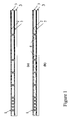
- Figure 1 is a schematic representing a standard Cu single damascene (SD) stack before (a) and after (b) etch of sacrificial material between narrowly spaced interconnects (1).
- Typical interconnects are metals (ie. Cu, Au, Ag%) embedded in a (3) SiO 2 and (2) SiC stack. (4) Are selectively incorporated airgaps.
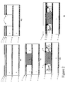
- Figure 2 (a) is a schematic representing the starting stack after resist coating and deep ultra violet (DUV) patterning (5).
- Figure 2 (b) shows the stack (a) after undergoing oxygen containing plasma exposure leading to a local oxidation of the SiC layer (7).
- Figure 2 (c) is the former stack after barrier deposition (ie. Ta/TaN (10/15 nm), Cu seed layer deposition (100 nm), Cu electroplating (1 ⁇ m) and chemical mechanical polishing (CMP).
- barrier deposition ie. Ta/TaN (10/15 nm
- Cu seed layer deposition 100 nm
- Cu electroplating 1 ⁇ m
- CMP chemical mechanical polishing
- Figure 2 (d) is after vapour HF (VHF) exposure (8) generating air cavities near the SiO 2 /TaN interface.
- VHF vapour HF
- Figure 2 (e) is after a thick conformal CVD layer (ie. SiC/SiO 2 CVD) has been deposited on top.
- a thick conformal CVD layer ie. SiC/SiO 2 CVD
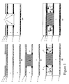
- Figure 3 is a schematic representing the starting stack after resist coating and deep ultra violet (DUV) patterning (5).
- (9) Is a CVD or spin on material resistant to HF exposure (ie. Silicon oxycarbide SiCOH).
- layer (9), also referred to as the basis layer, is preferably resistant to the second etching substance, this way the etching of the hole in the stack of layers is downwards limited by the basis layer.
- the basis layer is also preferably resistant to the first etching substance limiting the creation of airgaps. Preferably no airgap is formed in the basis layer (9).
- Figure 3 (b) shows the stack (a) after undergoing oxygen containing plasma exposure leading to a local oxidation of the SiC layer (7).
- Figure 3 (c) is the former stack after barrier deposition (i.e. Ta/TaN (10/15 nm), Cu seed layer deposition (100 nm), Cu electroplating (1 ⁇ m) and chemical mechanical polishing (CMP).
- barrier deposition i.e. Ta/TaN (10/15 nm
- Cu seed layer deposition 100 nm
- Cu electroplating 1 ⁇ m
- CMP chemical mechanical polishing
- Figure 3 (d) is after VHF exposure (8) generating air cavities near the SiO 2 /TaN interface. Note that the underlying material is not etched by HF, which is intended to confine the airgap cavities to a single level.
- Figure 3 (e) is after a thick conformal CVD layer (ie. SiC/SiO 2 CVD) has been deposited on top.
- a thick conformal CVD layer ie. SiC/SiO 2 CVD
- Figure 3 and Fig. 4 differ in the fact that an extra SiC layer(2) is deposited after etching the opening in the SiO 2 material. After deposition of said extra SiC layer, the bottom of said extra SiC layer is opened by etching and subsequent a barrier layer (i.e. Ta/TaN (10/15 nm) and a Cu seed layer (100 nm) are deposited prior to Cu electroplating (1 ⁇ m) and chemical mechanical polishing (CMP).
- a barrier layer i.e. Ta/TaN (10/15 nm
- a Cu seed layer 100 nm
- CMP chemical mechanical polishing
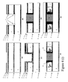
- Figure 4i and Figure 4ii differ in the fact that the basis layer (9) comprises further a metal structure.
- This metal structure is preferably making contact with the conductive line created in the hole etched in sacrificial layer (3). Finally this structure will lead to a damascene structure.
- Figure 4 (a) is a schematic representing the starting stack after resist coating and deep ultra violet (DUV) patterning (5).
- Figure 4 (b) shows the stack (a) after a dry etch operation in an O 2 containing plasma.
- Figure 4 (c) is the former stack after an extra SiC layer (i.e. 50 nm) has been deposited.
- Figure 4 (d) is after an isotropic oxygen plasma treatment with the aim of opening the bottom of the SiC layer.
- the etching of the hole is stopped on the basis layer (9)
- Figure 4ii the etching of the hole is stopped on the metal structure embedded in the basis layer (9).
- Figure 4 (e) is after deposition of a barrier (ie. Ta/TaN (10/15 nm), Cu seed layer deposition (100 nm) and Cu electroplating (1 ⁇ m) followed by (CMP) and HF vapour exposure, generating air cavities (4).
- a barrier ie. Ta/TaN (10/15 nm
- Cu seed layer deposition 100 nm
- Cu electroplating 1 ⁇ m
- CMP HF vapour exposure
- Figure 4 (f) is after a thick conformal CVD layer (ie. SiC/SiO 2 CVD) has been deposited on top of the air cavities (4).
- a thick conformal CVD layer ie. SiC/SiO 2 CVD
- Figure 5 is a cross-sectional TEM image of the Cu/SiO 2 single damascene stack at low (a) and high (b) magnification, (10) and (11) correspond to a protective platinum and glass layers respectively. (12) refers to the Si substrate. (c) Correspond to C (13), Cu (14) and O (15) EFTEM mappings of the area surrounded by the white dotted square on (a). Note that in EFTEM analysis light zones refer to high element concentrations. The white dotted circles denote converted SiC regions (plugs).
- Figure 6 are cross-sectional FIB images of a standard Cu-SiO 2 single damascene stack after (i) 4 and (ii) 8 minutes of VHF etch.
- (a) Represents a narrow line (low area), while (b) stands for a bondpad (large area). The x-direction is indicated on the figure.
- Figure 7 is a plot showing the etched distance (half of actual groove in x-direction) vs. time dependence of narrow lines and bond paths.
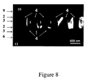
- Figure 8 is a schematic representing the SD stack after an arbitrary VHF exposure time leading to the incorporation of an airgap underneath a Cu line.
- the preferential channels of HF diffusion are shown by black dots at the SiC / Ta(N) interface.
- Figure 9 is a schematic representing the SD stack after an arbitrary VHF exposure time leading to the incorporation of airgaps between narrowly spaced (300 mm) lines.
- (16) refers to a SiC (50 nm) - SiO 2 (300 nm) - Si 3 N 4 (500 nm) layer on top of the airgap structure.
- Figure 10 shows an additional process flow for airgap formation to illustrate the practical examples.
- Figure 12 shows the interline capacitance versus nominal spacing after airgap formation with two different HF exposure times compared to samples without airgap formation.
- Figure 13 shows interline capacitance versus nominal spacing for samples with and without airgaps. Bars represent the capacitance drop due to airgaps. The drop in capacitance appears to be dependent on the spacing between two adjacent copper lines. This is because wider spaces allow accommodating bigger air cavities than smaller ones.
- the present invention provides a method for the production of airgaps in a semiconductor device, the semiconductor device comprising a substrate layer and a stack of layers on top of the substrate layer, the stack of layers comprising at least one iteration of a sub-stack of layers, the sub-stack of layers comprising;
- a method of the present invention for making airgaps in a stack of layers of a semiconductor device comprises the steps of:
- step (c) comprises the sub-steps of:
- Said sacrificial material can also be referred to as insulator material or dielectric material.
- said (at least one) sacrificial layer is a dielectric layer which is situated under said (at least one) liner layer.
- the liner layer situated upon said sacrificial layer has a function of (acts as) a hardmask layer.
- Said liner layer situated upon said sacrificial layer can thus be referred to as a hardmask layer.
- the liner layer in said stack of layers when situated under said sacrificial layer, can act as etch stop layer, but this is not compulsory.
- the liner layer situated upon said sacrificial layer is locally converted by said second etching substance and the etching of the hole is stopped on the liner layer situated under said sacrificial layer.
- the liner layer situated under said sacrificial layer is then acting as an etch stop layer.
- both the liner layer upon said sacrificial layer (acting as hardmask layer) and the liner layer under said sacrificial layer (this layer is opened during the etching of the hole) are locally converted by said second etching substance.
- the creation of the line in the hole can be performed by any standard technique.
- step (c) comprises the sub-steps of:
- Examples of said subtractive technique are Chemical Mechanical polishing (CMP), Electro Polishing, etch or any combination of these mentioned techniques.
- CMP Chemical Mechanical polishing
- Electro Polishing etch or any combination of these mentioned techniques.
- barrier layers are TaN, Ta, TiN, Ti, WN, WCN etc. These barrier layers can be deposited by Physical Vapour Deposition (PVD), Chemical Vapour Deposition (CVD), Metal Organic Chemical Vapour Deposition (MO-CVD), Atomic Layer Deposition (ALD) and related methods.
- PVD Physical Vapour Deposition
- CVD Chemical Vapour Deposition
- MO-CVD Metal Organic Chemical Vapour Deposition
- ALD Atomic Layer Deposition
- This barrier layer can have a function of diffusion barrier to avoid diffusion of the conductive material in to the dielectricum (e.g. low-k material).
- an additional step of depositing a protective layer on the exposed part of the line before step (d) is performed can be preferred.
- the conductive material is selected from the group of [metals, carbon nanotubes, conducting polymers].
- the conductive material can be for example Cu, Au or Ag.
- conductive lines are preferably part of a (single or dual) damascene structure in a semiconductor device.
- This dual damascene structure is made of horizontal lines (also referred to as “trenches”) and vertical structures (referred to as "vias”).
- Single and dual damascene structures are situated in the back end of line (BEOL) of semiconductor processing.
- Airgaps of the present invention can be preferably formed preferably near the trenches or preferably near the vias or preferably near vias and trenches. Most preferred the airgaps of the present invention are created near the vias.
- airgaps for electrical isolation purposes is an aim of the present invention, but airgaps can also be created in other contexts as for instance in the context of MEMS devices, where the airgap can be part of structurally or functionally.
- the steps of etching a hole in the stack of layers, and chemically changing the properties of the liner layers locally, are performed at the same time.
- said step (a) of etching a hole and said step (b) of converting said liner material (2) into a material (7) that is etchable by said first etching composition are simultaneous.
- the liner layer is a hardmask layer and the liner material is silicon carbide (SiC).
- the sacrificial layer material is a dielectric layer.
- the dielectric layer material is silicon dioxide (SiO 2 ).
- said sacrificial layer material is deposited upon a Si 3 N 4 layer (6), which can be referred to as an adhesion layer.
- the liner layer (e.g. SiC) material is converted locally into the sacrificial material (e.g. SiO 2 ).
- the chemically changed part of the liner layer has preferably in-plane dimensions smaller than 1 ⁇ m, more preferably 500 nm, even more preferably 100 nm. In-plane dimensions of smaller than 10 nm are easily possible.
- the stack of layers can be typically a single or dual damascene stack, but is not limited thereto.
- the stack of layers further comprises a basis layer.
- the basis layer (9) is resistant to the second etching substance, this way the etching of the hole in the stack of layers is downwards limited by the basis layer.
- the basis layer can thus also be an etch stop layer.
- the basis layer can comprise metal.
- An example of basis layer (9) resistant to said second etching composition (or substance) can be an organic low-k material.
- Other examples are silicon oxycarbide (SiCOH) materials rich in carbon molecules. The richer in carbon, the more resistant to said second etching substance is comparison with a silicon oxycarbide material used for said sacrificial layer (3).
- the basis layer is resistant to the first etching substance, which can be downwards limiting the formation of the airgaps.
- the second etching substance is an oxidizing substance.
- the second etching substance comprises O 2 .
- the second etching substance is a dry etch plasma comprising oxygen.
- the first etching substance comprises hydrofluoric acid (HF).
- HF hydrofluoric acid
- the etching can be performed preferably in an HF vapour ambient but also an HF dip in a diluted HF solution is possible.
- an anhydrous HF solution instead of an aqueous HF solution (HF/H 2 O mixture) is preferred because this is easier to control.
- anhydrous HF solutions are HF/alcolhol (e.g. methanol) mixtures.
- the hole is located at the back end of line.
- the basis layer comprises en embedded metal line.
- the embedded metal line and the metal line are forming an electrical contact.
- the method according to the present invention can be repeated. It is shown that on top af an airgap structure new layers can be formed, on which the method according to the present invention can be repeated.
- the method for the production of airgaps comprises the steps of:
- Figure 1 represents a standard Cu single damascene (SD) stack before (a) and after (b) etch of sacrificial material between narrowly spaced interconnects (1).
- Typical interconnects are metals (ie. Cu, Au, Ag%) embedded in a (3) dielectric stack which also contains liners (2).
- the dielectric material and liner are deposited on a Si or other substrate (which is not shown in the Figures) by a method such as Plasma Enhanced Chemical Vapour Deposition (PECVD), Chemical Vapour Deposition (CVD), spin-on deposition etc.
- PECVD Plasma Enhanced Chemical Vapour Deposition
- CVD Chemical Vapour Deposition
- said sacrificial layer (3) is made of SiOC:H material
- the carbon content should be low (enough) so that the etching step by said first etching composition is not hampered.
- liner layer (2) is any carbon containing Si compound such as SiC, SiC:H etc.
- items (4) represent selectively incorporated airgaps.
- the liner layer (2) situated upon sacrificial layer (3) has preferably the function of a hardmask layer.
- metal lines (1) for instance Cu lines, are embedded in a sacrificial material (3) (i.e. SiO 2 ).
- the metal lines (1) are typically further separated from the sacrificial material (3) by a barrier layer (not shown in the figures), as for instance a Ta/Ta(N) barrier.
- This barrier layer can have a function as diffusion barrier.
- a liner (hard mask) (2) is deposited on top (for instance SiC), which is resistant to etching agents for the sacrificial layer material (for instance HF) and is preferrably non-conducting.
- An induced local conversion of the liner, before the creation of the metal line (1) has to be performed (possible at nanometer scale), generating vulnerable spots (plugs).
- the plugs are expected to act as preferential channels for chemical diffusion metal line and typically also a barrier layer is deposited.
- a dissolution of the sacrificial material follows by applying the etching agent. This takes place preferentially between narrowly spaced Cu lines.
- the overburden of said deposited metal (conductive material) and the overburden of said barrier material are removed and planarized with standard removal techniques such as Chemical Mechanical Polishing (CMP).
- CMP Chemical Mechanical Polishing
- FIG. 2 A preferred embodiment of the present invention is as follows: the starting point of the process is a standard Cu single or dual damascene stack as described in Figure 2a. The dry etch step takes place in an O 2 containing plasma and leads to local oxidation of the liner (i.e. SiC) ( Figure 2b).
- the liner i.e. SiC
- the dry etch sequence for formation of vias and trenches, starts with an oxygen/fluorcarbon plasma with a high amount of oxygen to open the hardmask and subsequently a less oxygen rich plasma is applied (higher amount of fluorocarbon) to create an opening in the Si containing insulator (e.g. SiO 2 ).
- an oxygen/fluorcarbon plasma with a high amount of oxygen to open the hardmask and subsequently a less oxygen rich plasma is applied (higher amount of fluorocarbon) to create an opening in the Si containing insulator (e.g. SiO 2 ).
- the dry etch process is anisotropic which means that the lateral etching is negligible compared to the vertical etching.
- the anisotropic etch process is performed until the liner layer (2) situated under the Si containing insulator layer (3) (also referred to as sacrificial layer) is reached.
- the liner layer (2) situated under the sacrificial layer (3) is acting here as an etch stop layer.
- Both liner layers are preferably SiC.
- a part of the hardmask layer e.g. SiC
- SiO 2 oxygen rich plasma
- the dimensions of the converted part of the SiC hardmask is in the nanometer range, preferably 100 nm or smaller.
- the liner layer (2) acting as etch stop layer is preferably not converted by the oxygen rich plasma.
- Figure 2c shows the stack after barrier layer deposition (Ta/TaN (10/15 nm)), Cu seed layer deposition (100 nm), Cu electroplating (1 ⁇ m) and chemical mechanical polishing (CMP).
- barrier layer deposition Ti/TaN (10/15 nm)
- Cu seed layer deposition 100 nm
- Cu electroplating 1 ⁇ m
- CMP chemical mechanical polishing
- Typical examples for barrier are TaN, Ta, TiN, Ti, WN, WCN etc.
- PECVD Plasma Enhanced Chemical Vapour Deposition
- CVD Chemical Vapour Deposition
- Figure 2 (d) is after dielectric etching employing for instance vapour HF (VHF) (or any other compound etching the dielectric) (8) generating air cavities (4) near the dielectric / barrier interface.
- VHF vapour HF
- the range of SiC/SiO 2 conversion is in the nanometer range which is sufficient to allow diffusion of HF molecules to the underlying SiO 2 layers.
- This is a Ta(N)/SiC interface dependent process results in accelerated dissolution of SiO 2 laying between narrowly spaced Cu lines, compared to bare SiO 2 (existing between largely spaced Cu lines).
- the resulting stack is mechanically and chemically stable to allow further processing as depicted in Figure 2e. In the latter figure a thick conformal layer, such as liner or dielectric (2)/(3), has been deposited on top of the air cavities.
- FIGURE 3 Another preferred embodiment of the present invention is as follows:
- the starting point is a standard Cu single or dual damascene stack as described in Figure 3a, with a difference being the presence of a HF resistant layer (9) (i.e. Chemically deposited SiOC) as a basis layer under the Cu lines.
- a HF resistant layer 9 (i.e. Chemically deposited SiOC) as a basis layer under the Cu lines.
- the dry etch step takes place in an O 2 containing plasma, leading to local oxidation of the liner (7) (i.e. SiC) ( Figure 3b).
- the resulting stack is mechanically and chemically stable to allow further processing as depicted in Figure 3e. Note that no airgap is generated underneath the Cu lines allowing a better mechanical stability of the stack.
- the basis layer is preferably resistant to the second etching substance, this way the etching of the hole is downwards limited by the basis layer.
- This basis layer can comprise a metal structure.
- FIG. 4 Another preferred embodiment of the present invention (FIGURE 4) is as follows: The starting point is a standard Cu single or dual damascene stack as described in Figure 4a. The dry etch step takes place in an O 2 plasma (see Figure 4b) generating plugs at the SiC/Ta(N) interface ( Figure 4b). After resist strip, a supplementary conformal CVD SiC liner (i.e. 50 nm) is deposited, covering the whole exposed surface ( Figure 4c). An isotropic O 2 plasma treatment is then applied in order to open the bottom SiC as shown in Figure 4d. VHFwill diffuse through the induced plugs to the adjacent SiO 2 material, while leaving the Cu lines embodied with SiC ( Figure 4e). The resulting stack is mechanically and chemically stable to withstand further processing (Figure 4f).
- O 2 plasma see Figure 4b
- a supplementary conformal CVD SiC liner i.e. 50 nm
- An isotropic O 2 plasma treatment is then applied in order to open the bottom SiC
- the basis layer (9) is preferably resistant to the second etching etching substance, this way the etching of the hole is downwards limited by the basis layer (9).
- This basis layer can comprise a metal structure (as shown in Figure 4ii).
- the duration of the step of "chemically changing the properties of the liner layers locally” is less critical, as compared to duration of the step "applying the etching substance to the stack of layers".
- the airgap size can be controlled by a controlled duration of the step of "applying the etching substance to the stack of layers”.
- the distance between neighbouring conductor lines is determined by the limitations of state-of-the-art techniques with respect to forming neighbouring holes in the stack of layers.
- metal lines are spaced at about 1 ⁇ m .
- the present invention is a scaling invariant and is not limited to any distance between conductor lines, since the step of "chemically and/or mechanically changing the properties of the liner layers locally" can be applied on nanometer scale and smaller.
- Example 1 Practical example and process parameters
- a 200 mm wafer consisted of a standard single-damascene (SD) stack including a 600 nm SiO 2 on a 50 nm SiC liner lying on top of a 500 nm SiO 2 supported on a 50 nm Si 3 N 4 adhesion layer on a Si(100) as shown in Figure 2a.
- SD single-damascene
- the stack was dry etched until opening of the SiC layer as shown in Figure 2b.
- a 25 nm Ta(N) diffusion barrier (10 nm Ta(N), 15 nm Ta) and a 100 nm Cu seed layer were deposited by self ionised plasma (SIP).
- SIP self ionised plasma
- a-SiC:H amorphous hydrogenated SiC
- SiO 2 , SiH4 and N 2 O at 2.6 Torr served as precursors.
- the main mechanical characteristic of a-SiC:H (also referred to as BLOK or barrier low-k) is a +40 to +300 MPa stress
- the dry etch consisted according to the following conditions:- Pressure range:175 and 70 mTorr (double step SiO 2 etch) and 90 mTorr (SiC etch).
- chuck temperature is set at 20 degrees C; wafer temperature during dry etch sequence can ramp up to 70-80 degrees C depending on the process specifications and duration
- SiO 2 is etched in a 2-step sequence, including a main etch based on Ar, O 2 , CF 4 and CHF 3 (low SiO 2 /SiC selectivity) plus an additional overetch based on Ar, C 4 F 8 , O 2 .
- SiC is etched with a plasma composed on Ar, N 2 , CF 4 , CHF 3 .
- Etch time depends on the features size and depth, but typically takes ⁇ 60s for etching a 250nm wide trench over a depth of 600nm (SiO 2 main etch step).
- the strip was done in two steps (i) dry strip which employed vapour H 2 O and (ii) wet strip.
- Fig. 7 is a plot of etch rate vs. VHF exposure and Fig. 8 shows the resulting incorporated airgaps.
- Fig. 8 is a schematic of a typical cross-sectioned SD stack after VHF exposure.
- Example 2 Process flow for airgap formation
- FIG. 10 The overall process is shown in Figure 10.
- the stack composed of a 50/500/50/600/50 nm Si 3 N 4 /SiO 2 /SiC/SiO 2 /SiC was formed on a Si (100) wafer by plasma enhanced chemical vapor deposition (PE-CVD). Patterning was achieved by 248 nm wavelength optical lithography ( Figure 10a). Reactive ion etch (RIE) was carried out in an Ar/N 2 /O 2 /CF 4 /C 4 F 8 mixture at 70 mTorr. Resist strip was carefully controlled to induce local SiC oxidation at the sidewalls by using a H 2 O(v)/CF 4 gas mixture at 1100 mTorr ( Figure 10b).
- RIE reactive ion etch
- a 15/10 nm Ta/Ta(N) diffusion layer and a 100 nm Cu seed layer were formed by ionized physical vapor deposition (i-PVD). Trenches were filled by copper electroplating and the exceeding metal was removed by chemical mechanical polishing (CMP) as shown in Figure 10c. At this point the wafer was cut into 2 x 2 cm 2 dies. Single dies were exposed to an HF/Methanol gas phase mixture (HF(g)) by means of a MEMS-CET system (Primaxx, PA, USA) at low pressure.
- HF(g) HF/Methanol gas phase mixture
- HF(g) readily dissolves the locally oxidized SiC and diffuses through the Ta(N)/SiC interface leading to the dissolution of the underlying SiO 2 , and formation of full airgaps as depicted in Figure 10d.
- the amount of etched SiO 2 was mainly controlled by tuning the HF(g) exposure time. Gas temperature and pressure were also employed to finely tune the etch rate.
- Figure 11 shows cross-sectional FIB images of meander-fork structures.
- the airgaps appear to be formed as a result of an isotropic dissolution of the SiO 2 dielectric material as no preferred etching direction is observed.
- SiO 2 etch seems to be very selective avoiding any attack of the Ta/Ta(N) barrier.
- the top SiC layer remains in place even after a Pt layer is FIB deposited on top before imaging.
- Capacitance was measured between 1-2 cm long meanders and forks with nominal line width/spacing (L/S) comprised between 200/200 and 400/400 nm, using an HP4284A LCR meter at 100 kHz assuming a parallel RC model for the impedance. All experimental data are reported on Table 2. Capacitance (pF) data vs. etch time for samples after etching with HF.
- Example 4 Full size and half size airgaps between copper lines
- Figure 12 shows the capacitance performance for two sets of experiments leading to dies with full size (first set of experiment) and half size airgaps (second set of experiments).
- Half size airgaps correspond to air cavities equal to half the height of the copper line.
- samples with lower capacitance showed full airgaps, however samples with half size airgaps seemed to be much more stable than samples with full airgaps between the copper lines.
- the etch time or HF exposure time was not the only important factor to determine the size of the airgaps, also temperature and pressure of the chamber (different for the two sets of experiments) was important in determining the size of the airgaps.
- Example 5 TEM and EFTEM observations.
- FIG.5 A typical cross-sectional TEM image of the SD stack is shown in Fig.5 at low (a) and high (b) resolution.
- the right side of the sample in Fig. 5a corresponds to the thinnest part of the wedge as evidenced by its lighter contrast.
- the spherical profile of the SiC layer in the vicinity of the SiC / Ta(N) interface visible by TEM and supported by EFTEM suggest that this layer has been locally converted to SiO 2 importantly decreasing its contact area with the Ta(N) barrier wall. This SiC / SiO 2 conversion is ascribed to the action of the oxygen containing plasma employed at the dry etch step.
- Example 6 FIB, SEM and optical microscopy observations.
- Figure 6a shows typical FIB cross-sectional images of and isolated Cu line as the surrounding SiO 2 is gradually dissolved after VHF exposure.
- Half of the upper SiO 2 layer is removed after 4 mn of etch as shown in Fig.6ai.
- the underlying SiO 2 film is progressively removed underneath the SiC / Ta(N) interface (leading to the incorporation of air under the metal structure).
- the afore-mentioned phenomenon proved to take place selectively for SiO 2 material lying beneath any SiC / Ta(N) interface.
- the stack modification can be easily monitored by optical inspection.
- Figure 9 is a schematic representing the SD stack after an arbitrary VHF exposure time leading to the incorporation of airgaps between narrowly spaced (300 mm) lines. This figure shows that deposition of new layers on top of the airgap structure is possible.
- (16) refers to a SiC (50 nm) - SiO 2 (300 nm) -Si 3 N 4 (500 nm) layer.
Landscapes
- Internal Circuitry In Semiconductor Integrated Circuit Devices (AREA)
Abstract
- a first layer (2) made e.g. of SiC;
- a second layer (3) made of dielectric material;
- the second layer (3) is preferably situated under the first layer (2),
- the first layer (2) is preferably a hardmask layer
- the first layer material is resistant to a first etching substance;
- the first etching substance is able to etch the dielectric material;
- a) etching a hole in the stack of layers with a second etching substance,
- b) chemically changing the properties of the first layers (2) locally, whereby part of the first layers (2) is converted locally and becomes etchable by the first etching substance.
- c) creating in the hole a line (1) made of a conductive material, optionally separated from the dielectric layer (3) by a barrier layer, the line (1) or, if present, the barrier layer being resistant to the first etching substance;
- d) applying the first etching substance to the stack of layers whereby airgaps (4) are created around the line (1).
Description
- The present invention is related to the field of semiconductor processing.
- More specifically it is related to the production of micro and nano-electromechanical systems (MEMS, NEMS) and to the production of low dielectric isolation for interconnects.
- The present invention contributes to the exploration of the field of airgaps integration in semiconductor devices.
- The use of airgaps in semiconductor devices is known. Airgaps in the form of cavities can typically be present in MEMS and NEMS devices. Those airgaps can structurally be part of such a device or can have a functional role.
- Airgaps are considered to be very promising in the technology of interconnects, where they can be used as dielectric for isolation of interconnects. As IC technology scales down, the interconnect is becoming the most important restricting factor in terms of propagation delay, dynamic power consumption and signal errors originated by cross-talk effects between adjacent metal lines. The refocus from aluminium to copper has given an important reduction in the resistance of wired connections on the chip. At the moment, the aim is to achieve better isolation between the lines by introducing materials with lower dielectric constant than that of silicon oxide (k=4.2) leading to reducing the capacitance (C). The integration of low-k materials (k<3.0) into production processes creates a number of challenges associated with leakage, mechanical instability and joule heating, increasing the overall cost of future IC processes.
- Additionally, the barrier and intermediate layers tend to increase the effective permittivity of the final stack. Due to the aforementioned problems, and also because air is the best insulator available, a strong incentive exists to integrating airgaps between adjacent metal lines.
- The use of air as a dielectric to isolate electrical interconnects is known to reduce RC delay as well as dynamic power consumption and signal errors (e.g. cross-talk).
- Different ways of inducing air cavities are known in the art, for instance:
- (i) Isotropic Etching (for MEMS applications): consists of using HF for dissolving a sacrificial SiO2 layer, where other non-reacting film (i.e. SiC) is employed as an etch stop. The etch source is then sealed by a non-conformal CVD SiO2 layer.
- (ii) Anisotropic Etching: this consists of eliminating material by anisotropic dry etch, it is then necessary having a dedicated mask and adding the subsequent dry etch and strip operations. Subsequently a conformal CVD SiO2 followed by a non-conformal CVD SiO2 film are deposited on top of the lines responsible for the creation of airgaps.
-
- In US 6,268,261 a process for manufacturing a semiconductor circuit comprising airgaps is disclosed. The process comprises the steps of creating a plurality of adjacent conductive lines having a solid fill between the conductive lines; creating one or more layers above the lines and the fill; creating one or more pathways to the fill through the layers; and converting the fill to a gas that escapes through the pathways, leaving an air void between adjacent lines. The process results in a multi-layer semiconductor circuit comprising conductive lines, wherein the lines have air as a dielectric between them. Here a solid fill needs to be deposited inside between the conductive lines. This fill has to be stable during deposition of the layers on top. In the layers on top a pathway needs to be foreseen, which requires additional processing such as extra masking and etching steps.
- In US patent 6,599,814 a method is disclosed for removal of silicon carbide layers and in particular amorphous SiC of a substrate. Initially, the exposed part of a carbide-silicon layer is at least partly converted into an oxide-silicon layer by exposing the carbide-silicon layer to an oxygen containing plasma. The oxide-silicon layer is then removed from the substrate.
- It is an aim of the invention to provide a method, which allows to selectively introduce air between narrowly spaced adjacent metal lines.
- It is further an aim of the present invention to provide such a method, which is substantially scaling invariant.
- It is also an aim of the present invention to provide a method, which comprises a small number of process steps, compared to other state-of the art methods. More specifically it is an aim of the present invention to provide a process that does not introduce extra masking/stripping steps.
- The present invention provides a method for making airgaps (4) in a stack of layers of a semiconductor device, said stack of layers comprising:
- at least one layer of liner material (2) resistant to a first etching composition, and
- at least one layer of sacrificial material (3) etchable
by said first etching (substance or) composition,
said method comprising the steps of:
- a) etching at least one hole in said stack of layers with a second etching composition,
- b) chemically or mechanically converting said liner material (2), at least locally, into a material (7) that is etchable by said first etching substance,
- c) creating in said hole(s) a line (1) made of a conductive material, said line (1) being resistant to said first etching substance,
- d) contacting said first etching substance with said stack of layers whereby airgaps (4) are created around said line (1).
- In a method according to the invention, said sacrificial material (3) is preferably situated under said layer of liner material (2), or between two layers of said liner material (2).
- Preferably, step (c) of a method of the invention comprises the steps of:
- depositing a barrier layer,
- depositing on top of said barrier layer a layer of an electrically conductive material,
- removing on top of said stack of layers the overburden of said electrically conductive material and of said barrier layer.
- Preferably, said step (a) of etching at least one hole and said step (b) of converting said liner material (2) are simultaneous (are performed at the same time).
- Preferably, said conductive material is selected from the group of consisting of metals, carbon nanotubes, and conducting polymers. A metallic conductive material can be copper (Cu), gold (Au) or silver (Ag).
- In a method of the invention, said stack of layers can further comprise a basis layer (9), which can be resistant to said first etching composition, and/or resistant to said second etching composition.
- Said basis layer (9) can comprise an embedded metal line.
- In a method of the invention, the chemically and/or mechanically changed or converted part of said liner layers (7) have in-plane dimensions smaller than 1 µm, smaller than 500 nm, smaller than 100 nm, or smaller than 10 nm.
- In a method of the invention, said sacrificial material (3) is preferably silicon dioxide (SiO2).
- Said liner layer material is preferably silicon carbide (SiC).
- Said second etching substance or composition is preferably a dry etch plasma comprising O2, which may further comprise at least one (hydro)fluorocarbon compound, e.g. CF4, CHF3, and C4F8.
- Said first etching substance or composition preferably comprises or consists of hydrofluoric acid (HF), e.g. in a concentration of 49 wt.%.
- Said first etching substance or composition comprising or consisting of HF can be in vapour form.
- In a method of the invention, said stack of layers can be a single or dual damascene stack.
- In a method of the invention, said (at least one) hole is located at the back end of line.
- In a method of the invention, said embedded metal line in said basis layer (9) and said metal line (1) are forming an electrical contact.
- The present invention also provides a method for fabricating a semiconductor device having airgaps.
- The present invention also provides a method for the production of airgaps in a semiconductor device by repeating the steps of:
- applying a method according to the invention as described herein,
- creating a next stack of layers as described herein on top of the airgap structure resulting from the preceding step.
- The present invention also provides a device obtainable by a method of the invention.
- All drawings are intended to illustrate some aspects and embodiments of the present invention. Devices are depicted in a simplified way for reason of clarity. Not all alternatives and options are shown and therefore the invention is not limited to the content of the given drawings. Like numerals are employed to reference like parts in the different figures.
- Figure 1 is a schematic representing a standard Cu single damascene (SD) stack before (a) and after (b) etch of sacrificial material between narrowly spaced interconnects (1). Typical interconnects are metals (ie. Cu, Au, Ag...) embedded in a (3) SiO2 and (2) SiC stack. (4) Are selectively incorporated airgaps.
- Figure 2 (a) is a schematic representing the starting stack after resist coating and deep ultra violet (DUV) patterning (5).
- Figure 2 (b) shows the stack (a) after undergoing oxygen containing plasma exposure leading to a local oxidation of the SiC layer (7).
- Figure 2 (c) is the former stack after barrier deposition (ie. Ta/TaN (10/15 nm), Cu seed layer deposition (100 nm), Cu electroplating (1 µm) and chemical mechanical polishing (CMP).
- Figure 2 (d) is after vapour HF (VHF) exposure (8) generating air cavities near the SiO2/TaN interface.
- Figure 2 (e) is after a thick conformal CVD layer (ie. SiC/SiO2 CVD) has been deposited on top.
- Figure 3 (a) is a schematic representing the starting stack after resist coating and deep ultra violet (DUV) patterning (5). (9) Is a CVD or spin on material resistant to HF exposure (ie. Silicon oxycarbide SiCOH).
- Indeed, layer (9), also referred to as the basis layer, is preferably resistant to the second etching substance, this way the etching of the hole in the stack of layers is downwards limited by the basis layer.
- The basis layer is also preferably resistant to the first etching substance limiting the creation of airgaps. Preferably no airgap is formed in the basis layer (9).
- Figure 3 (b) shows the stack (a) after undergoing oxygen containing plasma exposure leading to a local oxidation of the SiC layer (7).
- Figure 3 (c) is the former stack after barrier deposition (i.e. Ta/TaN (10/15 nm), Cu seed layer deposition (100 nm), Cu electroplating (1 µm) and chemical mechanical polishing (CMP).
- Figure 3 (d) is after VHF exposure (8) generating air cavities near the SiO2/TaN interface. Note that the underlying material is not etched by HF, which is intended to confine the airgap cavities to a single level.
- Figure 3 (e) is after a thick conformal CVD layer (ie. SiC/SiO2 CVD) has been deposited on top.
- Figure 3 and Fig. 4 differ in the fact that an extra SiC layer(2) is deposited after etching the opening in the SiO2 material. After deposition of said extra SiC layer, the bottom of said extra SiC layer is opened by etching and subsequent a barrier layer (i.e. Ta/TaN (10/15 nm) and a Cu seed layer (100 nm) are deposited prior to Cu electroplating (1 µm) and chemical mechanical polishing (CMP).
- Figure 4i and Figure 4ii differ in the fact that the basis layer (9) comprises further a metal structure. This metal structure is preferably making contact with the conductive line created in the hole etched in sacrificial layer (3). Finally this structure will lead to a damascene structure.
- Figure 4 (a) is a schematic representing the starting stack after resist coating and deep ultra violet (DUV) patterning (5).
- Figure 4 (b) shows the stack (a) after a dry etch operation in an O2 containing plasma.
- Figure 4 (c) is the former stack after an extra SiC layer (i.e. 50 nm) has been deposited.
- Figure 4 (d) is after an isotropic oxygen plasma treatment with the aim of opening the bottom of the SiC layer. In figure 4i the etching of the hole is stopped on the basis layer (9), in Figure 4ii the etching of the hole is stopped on the metal structure embedded in the basis layer (9).
- Figure 4 (e) is after deposition of a barrier (ie. Ta/TaN (10/15 nm), Cu seed layer deposition (100 nm) and Cu electroplating (1 µm) followed by (CMP) and HF vapour exposure, generating air cavities (4).
- Figure 4 (f) is after a thick conformal CVD layer (ie. SiC/SiO2 CVD) has been deposited on top of the air cavities (4).
- Figure 5 is a cross-sectional TEM image of the Cu/SiO2 single damascene stack at low (a) and high (b) magnification, (10) and (11) correspond to a protective platinum and glass layers respectively. (12) refers to the Si substrate. (c) Correspond to C (13), Cu (14) and O (15) EFTEM mappings of the area surrounded by the white dotted square on (a). Note that in EFTEM analysis light zones refer to high element concentrations. The white dotted circles denote converted SiC regions (plugs).
- Figure 6 are cross-sectional FIB images of a standard Cu-SiO2 single damascene stack after (i) 4 and (ii) 8 minutes of VHF etch. (a) Represents a narrow line (low area), while (b) stands for a bondpad (large area). The x-direction is indicated on the figure.
- Figure 7 is a plot showing the etched distance (half of actual groove in x-direction) vs. time dependence of narrow lines and bond paths.
- Figure 8 is a schematic representing the SD stack after an arbitrary VHF exposure time leading to the incorporation of an airgap underneath a Cu line. The preferential channels of HF diffusion are shown by black dots at the SiC / Ta(N) interface.
- Figure 9 is a schematic representing the SD stack after an arbitrary VHF exposure time leading to the incorporation of airgaps between narrowly spaced (300 mm) lines. Here (16) refers to a SiC (50 nm) - SiO2 (300 nm) - Si3N4 (500 nm) layer on top of the airgap structure.
- Figure 10 shows an additional process flow for airgap formation to illustrate the practical examples.
- Figure 11 shows cross-sectional FIB images for structures with interline spacing of L/S = 200/200 nm, 250/250 nm, 300/300 nm and 400/400 nm. Air cavities are typically about half the height of the copper lines.
- Figure 12 shows the interline capacitance versus nominal spacing after airgap formation with two different HF exposure times compared to samples without airgap formation.
- Figure 13 shows interline capacitance versus nominal spacing for samples with and without airgaps. Bars represent the capacitance drop due to airgaps. The drop in capacitance appears to be dependent on the spacing between two adjacent copper lines. This is because wider spaces allow accommodating bigger air cavities than smaller ones.
- The present invention provides a method for the production of airgaps in a semiconductor device, the semiconductor device comprising a substrate layer and a stack of layers on top of the substrate layer, the stack of layers comprising at least one iteration of a sub-stack of layers, the sub-stack of layers comprising;
- a liner layer made of liner material;
- a sacrificial layer made of sacrificial layer material under the liner layer;
- the liner material is resistant to a first etching substance;
- the first etching substance is able to etch the sacrificial layer material;
- a) etching a hole in the stack of layers with a second etching substance,
- b) chemically and/or mechanically changing the properties of the liner layers locally, whereby part of the liner layers is converted locally and becomes becomes etchable by the first etching substance,
- c) creating in the hole a metal line made of a conductive material, optionally separated from the sacrificial layer by a barrier layer, the metal line or, if present, the barrier layer being resistant to the first etching substance,
- d) applying the first etching substance to the stack of layers whereby airgaps are created around the metal line.
- A method of the present invention for making airgaps in a stack of layers of a semiconductor device, wherein said stack of layers comprises at least one layer of liner material (2) resistant to a first etching substance or composition, and at least one layer of sacrificial material (3) etchable by said first etching substance or composition, comprises the steps of:
- a) etching at least one hole in said stack of layers with a second etching substance or composition,
- b) chemically or mechanically converting said liner material (2), at least locally, into a material (7) that is etchable by said first etching substance or composition,
- c) creating in said hole a line (1) made of a conductive material, said line (1) being resistant to said first etching substance or composition, and
- d) contacting said first etching substance with said stack of layers whereby airgaps (4) are created around said line (1).
-
- Preferably step (c) comprises the sub-steps of:
- (i) optionally depositing a barrier layer,
- (ii) depositing on top of the barrier layer a layer of electrically conductive material,
- (iii) applying a subtractive technique on top of the stack of layers whereby at least 1 embedded line is created.
-
- Said sacrificial material can also be referred to as insulator material or dielectric material.
- Preferably said (at least one) sacrificial layer is a dielectric layer which is situated under said (at least one) liner layer.
- Preferably the liner layer situated upon said sacrificial layer has a function of (acts as) a hardmask layer.
- Said liner layer situated upon said sacrificial layer can thus be referred to as a hardmask layer.
- The liner layer in said stack of layers, when situated under said sacrificial layer, can act as etch stop layer, but this is not compulsory.
- In preferred embodiments only the liner layer situated upon said sacrificial layer is locally converted by said second etching substance and the etching of the hole is stopped on the liner layer situated under said sacrificial layer. The liner layer situated under said sacrificial layer is then acting as an etch stop layer.
- In another preferred embodiment, both the liner layer upon said sacrificial layer (acting as hardmask layer) and the liner layer under said sacrificial layer (this layer is opened during the etching of the hole) are locally converted by said second etching substance.
- The creation of the line in the hole can be performed by any standard technique.
- Preferably step (c) comprises the sub-steps of:
- (i) depositing a barrier layer,
- (ii) depositing on top of the barrier layer a layer of electrically conductive material,
- (iii) removing the overburden of conductive material and barrier layer by applying a subtractive technique on top of the stack of layers whereby at least 1 embedded line is created.
-
- Examples of said subtractive technique are Chemical Mechanical polishing (CMP), Electro Polishing, etch or any combination of these mentioned techniques.
- Examples of barrier layers are TaN, Ta, TiN, Ti, WN, WCN etc. These barrier layers can be deposited by Physical Vapour Deposition (PVD), Chemical Vapour Deposition (CVD), Metal Organic Chemical Vapour Deposition (MO-CVD), Atomic Layer Deposition (ALD) and related methods. This barrier layer can have a function of diffusion barrier to avoid diffusion of the conductive material in to the dielectricum (e.g. low-k material).
- In case the conducting material of the line is not resistant to the first etching substance and a barrier layer is present, an additional step of depositing a protective layer on the exposed part of the line before step (d) is performed can be preferred.
- Preferably the conductive material is selected from the group of [metals, carbon nanotubes, conducting polymers]. The conductive material can be for example Cu, Au or Ag.
- Preferably the filling of the holes leads to the creation of conductive lines. These conductive lines are preferably part of a (single or dual) damascene structure in a semiconductor device. This dual damascene structure is made of horizontal lines (also referred to as "trenches") and vertical structures (referred to as "vias"). Single and dual damascene structures are situated in the back end of line (BEOL) of semiconductor processing.
- Airgaps of the present invention can be preferably formed preferably near the trenches or preferably near the vias or preferably near vias and trenches. Most preferred the airgaps of the present invention are created near the vias.
- The production of airgaps for electrical isolation purposes is an aim of the present invention, but airgaps can also be created in other contexts as for instance in the context of MEMS devices, where the airgap can be part of structurally or functionally.
- In preferred embodiments the steps of etching a hole in the stack of layers, and chemically changing the properties of the liner layers locally, are performed at the same time.
- In other words, preferably, said step (a) of etching a hole and said step (b) of converting said liner material (2) into a material (7) that is etchable by said first etching composition, are simultaneous.
- In preferred embodiment the liner layer is a hardmask layer and the liner material is silicon carbide (SiC).
- In preferred embodiment the sacrificial layer material is a dielectric layer. Most preferred the dielectric layer material is silicon dioxide (SiO2).
- Preferably, said sacrificial layer material is deposited upon a Si3N4 layer (6), which can be referred to as an adhesion layer.
- In preferred embodiments the liner layer (e.g. SiC) material is converted locally into the sacrificial material (e.g. SiO2).
- The chemically changed part of the liner layer has preferably in-plane dimensions smaller than 1 µm, more preferably 500 nm, even more preferably 100 nm. In-plane dimensions of smaller than 10 nm are easily possible.
- The stack of layers can be typically a single or dual damascene stack, but is not limited thereto.
- In specific embodiments the stack of layers further comprises a basis layer.
- Preferably the basis layer (9) is resistant to the second etching substance, this way the etching of the hole in the stack of layers is downwards limited by the basis layer. The basis layer can thus also be an etch stop layer.
- The basis layer can comprise metal.
- An example of basis layer (9) resistant to said second etching composition (or substance) can be an organic low-k material. Other examples are silicon oxycarbide (SiCOH) materials rich in carbon molecules. The richer in carbon, the more resistant to said second etching substance is comparison with a silicon oxycarbide material used for said sacrificial layer (3).
- In certain embodiments according to the present invention, the basis layer is resistant to the first etching substance, which can be downwards limiting the formation of the airgaps.
- In preferred embodiments, the second etching substance is an oxidizing substance.
- In preferred embodiment the second etching substance comprises O2.
- In preferred embodiments, the second etching substance is a dry etch plasma comprising oxygen.
- In preferred embodiment the first etching substance comprises hydrofluoric acid (HF). The etching can be performed preferably in an HF vapour ambient but also an HF dip in a diluted HF solution is possible.
- In case the first etching substance is an HF solution, an anhydrous HF solution instead of an aqueous HF solution (HF/H2O mixture) is preferred because this is easier to control. Examples of the anhydrous HF solutions are HF/alcolhol (e.g. methanol) mixtures.
- In preferred embodiment the hole is located at the back end of line.
- In preferred embodiment the basis layer comprises en embedded metal line.
- In preferred embodiment the embedded metal line and the metal line are forming an electrical contact.
In preferred embodiments the method according to the present invention can be repeated. It is shown that on top af an airgap structure new layers can be formed, on which the method according to the present invention can be repeated. - The method for the production of airgaps comprises the steps of:
- a) plasma dry etching a hole in the stack of layers with a second etching substance,
- b) chemically changing the properties of the liner layer locally, whereby part of the liner layer is converted locally and becomes etchable by the first etching substance,
- c) creating in the hole a line made of a conductive material, optionally separated from the sacrificial layer by a barrier layer, the line or, if present, the barrier layer being resistant to the first etching substance,
- d) applying the first etching substance to the stack of layers whereby airgaps are created around the line.
-
- Figure 1 represents a standard Cu single damascene (SD) stack before (a) and after (b) etch of sacrificial material between narrowly spaced interconnects (1). Typical interconnects are metals (ie. Cu, Au, Ag...) embedded in a (3) dielectric stack which also contains liners (2). The dielectric material and liner are deposited on a Si or other substrate (which is not shown in the Figures) by a method such as Plasma Enhanced Chemical Vapour Deposition (PECVD), Chemical Vapour Deposition (CVD), spin-on deposition etc.
- Layer (3) is typically SiO2 (k= 4.2) or another Si containing insulator material with lower k value such as SiOC:H materials (Carbon doped oxides, commonly referred to as silicon oxy carbides).
- When said sacrificial layer (3) is made of SiOC:H material, the carbon content should be low (enough) so that the etching step by said first etching composition is not hampered.
- An example for the liner layer (2) is any carbon containing Si compound such as SiC, SiC:H etc. In Fig. 1 items (4) represent selectively incorporated airgaps.
- The liner layer (2) situated upon sacrificial layer (3) has preferably the function of a hardmask layer.
- In preferred embodiments according to the present invention metal lines (1), for instance Cu lines, are embedded in a sacrificial material (3) (i.e. SiO2). The metal lines (1) are typically further separated from the sacrificial material (3) by a barrier layer (not shown in the figures), as for instance a Ta/Ta(N) barrier. This barrier layer can have a function as diffusion barrier. A liner (hard mask) (2) is deposited on top (for instance SiC), which is resistant to etching agents for the sacrificial layer material (for instance HF) and is preferrably non-conducting. An induced local conversion of the liner, before the creation of the metal line (1), has to be performed (possible at nanometer scale), generating vulnerable spots (plugs). For instance a localised plasma conversion of the SiC liner into SiO2. The plugs are expected to act as preferential channels for chemical diffusion metal line and typically also a barrier layer is deposited. A dissolution of the sacrificial material follows by applying the etching agent. This takes place preferentially between narrowly spaced Cu lines.
- The overburden of said deposited metal (conductive material) and the overburden of said barrier material are removed and planarized with standard removal techniques such as Chemical Mechanical Polishing (CMP).
- A way to selectively introduce air between narrowly spaced Cu interconnects in a single step is disclosed being fully compatible with the back end of line process as illustrated in Figure 1.
- A preferred embodiment of the present invention (Figure 2) is as follows: the starting point of the process is a standard Cu single or dual damascene stack as described in Figure 2a. The dry etch step takes place in an O2 containing plasma and leads to local oxidation of the liner (i.e. SiC) (Figure 2b).
- The dry etch sequence, for formation of vias and trenches, starts with an oxygen/fluorcarbon plasma with a high amount of oxygen to open the hardmask and subsequently a less oxygen rich plasma is applied (higher amount of fluorocarbon) to create an opening in the Si containing insulator (e.g. SiO2 ).
- The dry etch process is anisotropic which means that the lateral etching is negligible compared to the vertical etching.
- The anisotropic etch process is performed until the liner layer (2) situated under the Si containing insulator layer (3) (also referred to as sacrificial layer) is reached.
- The liner layer (2) situated under the sacrificial layer (3) is acting here as an etch stop layer.
- Both liner layers (hardmask and etch stop layer) are preferably SiC.
- During the dry etching process, a part of the hardmask layer (e.g. SiC), situated at the sidewall of the opening, is due to the oxygen rich plasma oxidised to SiO2.
- The dimensions of the converted part of the SiC hardmask is in the nanometer range, preferably 100 nm or smaller.
- The liner layer (2) acting as etch stop layer is preferably not converted by the oxygen rich plasma.
- Figure 2c shows the stack after barrier layer deposition (Ta/TaN (10/15 nm)), Cu seed layer deposition (100 nm), Cu electroplating (1 µm) and chemical mechanical polishing (CMP). Typical examples for barrier are TaN, Ta, TiN, Ti, WN, WCN etc. Currently employed methods for depositing a barrier are Plasma Enhanced Chemical Vapour Deposition (PECVD), Chemical Vapour Deposition (CVD), spin-on deposition etc. Figure 2 (d) is after dielectric etching employing for instance vapour HF (VHF) (or any other compound etching the dielectric) (8) generating air cavities (4) near the dielectric / barrier interface. The range of SiC/SiO2 conversion is in the nanometer range which is sufficient to allow diffusion of HF molecules to the underlying SiO2 layers. The fact that this is a Ta(N)/SiC interface dependent process results in accelerated dissolution of SiO2 laying between narrowly spaced Cu lines, compared to bare SiO2 (existing between largely spaced Cu lines). The resulting stack is mechanically and chemically stable to allow further processing as depicted in Figure 2e. In the latter figure a thick conformal layer, such as liner or dielectric (2)/(3), has been deposited on top of the air cavities.
- Another preferred embodiment of the present invention (FIGURE 3) is as follows:
- As in the first embodiment, the starting point is a standard Cu single or dual damascene stack as described in Figure 3a, with a difference being the presence of a HF resistant layer (9) (i.e. Chemically deposited SiOC) as a basis layer under the Cu lines. The dry etch step takes place in an O2 containing plasma, leading to local oxidation of the liner (7) (i.e. SiC) (Figure 3b). The resulting stack is mechanically and chemically stable to allow further processing as depicted in Figure 3e. Note that no airgap is generated underneath the Cu lines allowing a better mechanical stability of the stack.
- The basis layer is preferably resistant to the second etching substance, this way the etching of the hole is downwards limited by the basis layer. This basis layer can comprise a metal structure.
- Another preferred embodiment of the present invention (FIGURE 4) is as follows: The starting point is a standard Cu single or dual damascene stack as described in Figure 4a. The dry etch step takes place in an O2 plasma (see Figure 4b) generating plugs at the SiC/Ta(N) interface (Figure 4b). After resist strip, a supplementary conformal CVD SiC liner (i.e. 50 nm) is deposited, covering the whole exposed surface (Figure 4c). An isotropic O2 plasma treatment is then applied in order to open the bottom SiC as shown in Figure 4d. VHFwill diffuse through the induced plugs to the adjacent SiO2 material, while leaving the Cu lines embodied with SiC (Figure 4e). The resulting stack is mechanically and chemically stable to withstand further processing (Figure 4f).
- Preferably no airgaps are formed in the basis layer (9). The basis layer (9) is preferably resistant to the second etching etching substance, this way the etching of the hole is downwards limited by the basis layer (9). This basis layer can comprise a metal structure (as shown in Figure 4ii).
- When one considers the size of created airgaps (4) as a measure, the duration of the step of "chemically changing the properties of the liner layers locally" is less critical, as compared to duration of the step "applying the etching substance to the stack of layers". Independent of the size of the area of the liner layers which is chemically and/or mechanically changed, the airgap size can be controlled by a controlled duration of the step of "applying the etching substance to the stack of layers".
- The distance between neighbouring conductor lines is determined by the limitations of state-of-the-art techniques with respect to forming neighbouring holes in the stack of layers. Typically metal lines are spaced at about 1µm . The present invention is a scaling invariant and is not limited to any distance between conductor lines, since the step of "chemically and/or mechanically changing the properties of the liner layers locally" can be applied on nanometer scale and smaller.
- A 200 mm wafer consisted of a standard single-damascene (SD) stack including a 600 nm SiO2 on a 50 nm SiC liner lying on top of a 500 nm SiO2 supported on a 50 nm Si3N4 adhesion layer on a Si(100) as shown in Figure 2a. After lithography, the stack was dry etched until opening of the SiC layer as shown in Figure 2b. Subsequently a 25 nm Ta(N) diffusion barrier (10 nm Ta(N), 15 nm Ta) and a 100 nm Cu seed layer were deposited by self ionised plasma (SIP). The trenches were filled by Cu electroplating (Figure 2c) and the remaining material removed by chemical mechanical polishing (see Figure 2d).
- Organosilicon trimethylsilane gas and He at a pressure of ca. 8 Torr were employed as precursors for a-SiC:H (amorphous hydrogenated SiC). For SiO2, SiH4 and N2O at 2.6 Torr served as precursors. The main mechanical characteristic of a-SiC:H (also referred to as BLOK or barrier low-k) is a +40 to +300 MPa stress
- The dry etch consisted according to the following conditions:- Pressure range:175 and 70 mTorr (double step SiO2 etch) and 90 mTorr (SiC etch).
- - Temperature: chuck temperature is set at 20 degrees C; wafer temperature during dry etch sequence can ramp up to 70-80 degrees C depending on the process specifications and duration
- - Species:
- *SiO2 is etched in a 2-step sequence, including a main etch based on Ar, O2, CF4 and CHF3 (low SiO2/SiC selectivity) plus an additional overetch based on Ar, C4F8, O2.
- *SiC is etched with a plasma composed on Ar, N2, CF4, CHF3.
- - Etch time: depends on the features size and depth, but typically takes ~ 60s for etching a 250nm wide trench over a depth of 600nm (SiO2 main etch step).
- The strip was done in two steps (i) dry strip which employed vapour H2O and (ii) wet strip.
- Additionally, the samples underwent a well controlled SiO2 etch by using a HF solution (49 % clean room compatible). The amount of etched SiO2 can be easily controlled by the time and temperature employed. Fig. 7 is a plot of etch rate vs. VHF exposure and Fig. 8 shows the resulting incorporated airgaps. Fig. 8 is a schematic of a typical cross-sectioned SD stack after VHF exposure.
- The overall process is shown in Figure 10. In first place, the stack composed of a 50/500/50/600/50 nm Si3N4/SiO2/SiC/SiO2/SiC was formed on a Si (100) wafer by plasma enhanced chemical vapor deposition (PE-CVD). Patterning was achieved by 248 nm wavelength optical lithography (Figure 10a). Reactive ion etch (RIE) was carried out in an Ar/N2/O2/CF4/C4F8 mixture at 70 mTorr. Resist strip was carefully controlled to induce local SiC oxidation at the sidewalls by using a H2O(v)/CF4 gas mixture at 1100 mTorr (Figure 10b). Then a 15/10 nm Ta/Ta(N) diffusion layer and a 100 nm Cu seed layer were formed by ionized physical vapor deposition (i-PVD). Trenches were filled by copper electroplating and the exceeding metal was removed by chemical mechanical polishing (CMP) as shown in Figure 10c. At this point the wafer was cut into 2 x 2 cm2 dies. Single dies were exposed to an HF/Methanol gas phase mixture (HF(g)) by means of a MEMS-CET system (Primaxx, PA, USA) at low pressure. HF(g) readily dissolves the locally oxidized SiC and diffuses through the Ta(N)/SiC interface leading to the dissolution of the underlying SiO2, and formation of full airgaps as depicted in Figure 10d. The amount of etched SiO2 was mainly controlled by tuning the HF(g) exposure time. Gas temperature and pressure were also employed to finely tune the etch rate.
- Figure 11 shows cross-sectional FIB images of meander-fork structures. The airgaps appear to be formed as a result of an isotropic dissolution of the SiO2 dielectric material as no preferred etching direction is observed. Under the experimental conditions employed, SiO2 etch seems to be very selective avoiding any attack of the Ta/Ta(N) barrier. In addition, the top SiC layer remains in place even after a Pt layer is FIB deposited on top before imaging.
- Capacitance was measured between 1-2 cm long meanders and forks with nominal line width/spacing (L/S) comprised between 200/200 and 400/400 nm, using an HP4284A LCR meter at 100 kHz assuming a parallel RC model for the impedance. All experimental data are reported on Table 2.
Capacitance (pF) data vs. etch time for samples after etching with HF. L/S
(micron)HF etch time (minutes) 3 4 5 6 6 5 6 7 8 1-3 1-4 1-5 1-6 1--6-2 2-5 2-6 2-7 2-8 0.2/0.2 6.8 6.52 // 6 // 6.58 6.63 5.83 5.34 6.74 6.5 // 6.06 3.06 6.32 6.67 5.81 5.34 6.76 6.52 // 6.05 6.01 // 6.68 5.82 5.35 6.75 6.62 5.88 6.07 6.05 6.84 6.76 5.81 5.38 6.78 // // 6 // 6.82 6.69 5.79 5.36 // 6.59 5.82 5.86 5.86 6.97 6.69 5.79 5.35 average 6.766 6.55 5.85 6. 01 5.97 6.71 6.69 5.81 5.35 0.25/0.25 4.06 3.98 3.34 3.51 // 3.99 4.07 3.67 3.28 4.02 3.96 // 3.5 // 3.95 4.07 3.66 3.27 4.01 3.97 // 3.48 3.5 3.91 4.06 3.69 3.27 4.08 4.03 // 3.54 // 3.94 4.09 3.73 3.26 4.04 4.02 // 3.53 // 3.95 4.07 3.68 3.26 4.03 4.01 // 3.53 // 3.96 4.06 3.7 3.27 average 4.04 4.00 3.34 3.52 3.50 3.95 4.07 3.69 3.27 0.3/0.3 2.68 2.69 // 2.36 2.36 2.63 2.74 2.53 2.18 2.67 2.68 // 2.35 // 2.73 2.73 2.53 2.18 2.66 2.68 // 2.35 2.34 2.73 2.72 2.53 2.18 2.69 2.74 // 2.4 2.39 2.66 2.75 2.59 2.2 2.7 2.73 // 2.4 2.38 2.68 2.76 2.6 2.21 2.7 2.73 // 2.41 2.38 2.97 2.77 2.58 2.21 average 2.68 2.71 // 2.38 2.37 2.73 2.75 2.56 2.19 0.4/0.4 1.49 1.5 1.21 1.29 // 1.48 1.53 1.42 1.19 1.49 1.49 1.21 1.28 // 1.46 1.53 1.42 1.19 1.49 1.49 1.21 1.28 // 1.45 1.53 1.42 1.19 1.54 1.51 1.23 1.31 // 1.49 1.57 1.47 1.18 1.51 1.5 1.22 1.3 // 1.47 1.54 1.46 1.18 1.5 1.5 1.21 1.3 // 1.47 1.54 1.45 1.18 average 1.50 1.51 1.22 1.29 // 1.47 1.54 1.44 1.19 //: no data available - Figure 12 shows the capacitance performance for two sets of experiments leading to dies with full size (first set of experiment) and half size airgaps (second set of experiments). Half size airgaps correspond to air cavities equal to half the height of the copper line. As shown in Figure 12 samples with lower capacitance showed full airgaps, however samples with half size airgaps seemed to be much more stable than samples with full airgaps between the copper lines. The etch time or HF exposure time was not the only important factor to determine the size of the airgaps, also temperature and pressure of the chamber (different for the two sets of experiments) was important in determining the size of the airgaps.
- A typical cross-sectional TEM image of the SD stack is shown in Fig.5 at low (a) and high (b) resolution. The right side of the sample in Fig. 5a corresponds to the thinnest part of the wedge as evidenced by its lighter contrast. The spherical profile of the SiC layer in the vicinity of the SiC / Ta(N) interface visible by TEM and supported by EFTEM suggest that this layer has been locally converted to SiO2 importantly decreasing its contact area with the Ta(N) barrier wall. This SiC / SiO2 conversion is ascribed to the action of the oxygen containing plasma employed at the dry etch step.
- Figure 6a shows typical FIB cross-sectional images of and isolated Cu line as the surrounding SiO2 is gradually dissolved after VHF exposure. Half of the upper SiO2 layer is removed after 4 mn of etch as shown in Fig.6ai. As the HF exposure continues, the underlying SiO2 film is progressively removed underneath the SiC / Ta(N) interface (leading to the incorporation of air under the metal structure). The afore-mentioned phenomenon proved to take place selectively for SiO2 material lying beneath any SiC / Ta(N) interface. After prolonged HF etch times (more than ca. 8 mn) the stack modification can be easily monitored by optical inspection.
- Figure 9 is a schematic representing the SD stack after an arbitrary VHF exposure time leading to the incorporation of airgaps between narrowly spaced (300 mm) lines. This figure shows that deposition of new layers on top of the airgap structure is possible. Here (16) refers to a SiC (50 nm) - SiO2 (300 nm) -Si3N4 (500 nm) layer. This shows moreover that sacrificial layers, hardmask layers and if appropriate, basis layers can be formed on top of the airgap structure, after which the embodiments of the present invention can be repeated.
Claims (27)
- Method for making airgaps (4) in a stack of layers of a semiconductor device, said stack of layers comprising:said method comprising the steps of:at least one layer of liner material (2) resistant to a first etching composition, andat least one layer of sacrificial material (3) etchable by said first etching (substance or) composition,a) etching at least one hole in said stack of layers with a second etching composition,b) chemically or mechanically converting said liner material (2), at least locally, into a material (7) that is etchable by said first etching substance,c) creating in said hole(s) a line (1) made of a conductive material, said line (1) being resistant to said first etching substance,d) contacting said first etching substance with said stack of layers whereby airgaps (4) are created around said line (1). 1.
- A method according to claim 1, wherein said sacrificial material (3) is situated under said at least one layer of liner material (2).
- A method according to claim 1, wherein said at least one sacrificial material (3) is situated between two layers of said liner material (2).
- A method according to any of claims 1 to 3, wherein step (c) comprises the steps of:depositing a barrier layer,depositing on top of said barrier layer a layer of an electrically conductive material,removing on top of said stack of layers the overburden of said electrically conductive material and of said barrier layer.
- A method according to any of claims 1 to 4, wherein said step (a) of etching at least one hole and said step (b) of converting said liner material (2) are simultaneous.
- A method according to any of claims 1 to 5, wherein a protective layer is deposited on the exposed part of said line before said step (d) of contacting said first etching composition with said stack of layers is performed.
- A method according to any of claims 1 to 6, wherein said conductive material is selected from the group of consisting of metals, carbon nanotubes, and conducting polymers.
- A method according to claim 7, wherein said conductive material is Cu, Au or Ag.
- A method according to any of claims 1 to 8, wherein said stack of layers further comprises a basis layer (9).
- A method according to claim 9, wherein said basis layer (9) is resistant to said first etching composition.
- A method according to claim 9 or 10, wherein said basis layer (9) is resistant to said second etching composition.
- A method according to any of claims 9 to 11, wherein said basis layer (9) comprises an embedded metal line.
- A method according to any of claims 1 to 12, wherein the chemically and/or mechanically converted part of said liner layers (7) have in-plane dimensions smaller than 1 µm, smaller than 500 nm, smaller than 100 nm, or smaller than 10 nm.
- A method according to any of claims 1 to 13, wherein said sacrificial material (3) is silicon dioxide (SiO2).
- A method according to any of claims 1 to 14, wherein said liner layer material is silicon carbide (SiC).
- A method according to any of claims 1 to 15, wherein said second etching substance is a dry etch plasma comprising O2.
- A method according to claim 16, wherein said O2 comprising plasma further comprises at least one (hydro)fluorocarbon compound.
- A method according to claim 17, wherein said (hydro)fluorocarbon compound is selected from the group consisting of CF4, CHF3, and C4F8.
- A method according to any of claims 1 to 18, wherein said first etching composition comprises hydrofluoric acid (HF).
- A method according to any of claims 1 to 19, wherein said first etching composition consists of an solution of 49 wt.% HF.
- A method according to claim 19, wherein said HF is an HF vapour.
- A method according to any of claims 1 to 21, wherein said stack of layers is a single or dual damascene stack.
- A method according to any of claims 1 to 22, wherein said hole is located at the back end of line.
- A method according to any of claims 12 to 23, wherein said embedded metal line in basis layer (9) and said metal line (1) are forming an electrical contact.
- A method for fabricating a semiconductor device having airgaps comprising a method according to any of claims 1 to 24.
- A method for fabricating a semiconductor device having airgaps according to claim 25 wherein the following steps are repeated at least twice:carrying out a method according to any of claims 1 to 24, andcreating a next stack of layers on top of the airgap structure resulting from preceding step.
- A device obtainable by a method according to claim 25 or 26.
Priority Applications (1)
| Application Number | Priority Date | Filing Date | Title |
|---|---|---|---|
| EP04447220.7A EP1608013B1 (en) | 2003-09-30 | 2004-09-30 | Method of formation of airgaps around interconnecting line |
Applications Claiming Priority (5)
| Application Number | Priority Date | Filing Date | Title |
|---|---|---|---|
| US507584 | 1995-07-26 | ||
| US50758403P | 2003-09-30 | 2003-09-30 | |
| EP03447239 | 2003-09-30 | ||
| EP03447239A EP1521301A1 (en) | 2003-09-30 | 2003-09-30 | Method of formation of airgaps around interconnecting line |
| EP04447220.7A EP1608013B1 (en) | 2003-09-30 | 2004-09-30 | Method of formation of airgaps around interconnecting line |
Publications (2)
| Publication Number | Publication Date |
|---|---|
| EP1608013A1 true EP1608013A1 (en) | 2005-12-21 |
| EP1608013B1 EP1608013B1 (en) | 2013-04-24 |
Family
ID=34933094
Family Applications (1)
| Application Number | Title | Priority Date | Filing Date |
|---|---|---|---|
| EP04447220.7A Expired - Lifetime EP1608013B1 (en) | 2003-09-30 | 2004-09-30 | Method of formation of airgaps around interconnecting line |
Country Status (1)
| Country | Link |
|---|---|
| EP (1) | EP1608013B1 (en) |
Cited By (1)
| Publication number | Priority date | Publication date | Assignee | Title |
|---|---|---|---|---|
| FR3152913A1 (en) * | 2023-09-11 | 2025-03-14 | Centre National De La Recherche Scientifique | Method for producing MOSFET transistors integrating air cavities for reducing capacitive coupling in radiofrequency regime |
Citations (4)
| Publication number | Priority date | Publication date | Assignee | Title |
|---|---|---|---|---|
| US20020055243A1 (en) * | 2000-11-06 | 2002-05-09 | United Microelectronics Corp. | Gap-type metallic interconnect and method of manufacture |
| US6387818B1 (en) * | 2000-07-21 | 2002-05-14 | Advanced Micro Devices, Inc. | Method of porous dielectric formation with anodic template |
| US20020127844A1 (en) * | 2000-08-31 | 2002-09-12 | International Business Machines Corporation | Multilevel interconnect structure containing air gaps and method for making |
| US6599814B1 (en) * | 1999-05-03 | 2003-07-29 | Interuniversitair Microelektronica Centrum (Imec) | Method for removal of sic |
Family Cites Families (2)
| Publication number | Priority date | Publication date | Assignee | Title |
|---|---|---|---|---|
| US5818071A (en) * | 1995-02-02 | 1998-10-06 | Dow Corning Corporation | Silicon carbide metal diffusion barrier layer |
| US6403461B1 (en) * | 2001-07-25 | 2002-06-11 | Chartered Semiconductor Manufacturing Ltd. | Method to reduce capacitance between metal lines |
-
2004
- 2004-09-30 EP EP04447220.7A patent/EP1608013B1/en not_active Expired - Lifetime
Patent Citations (4)
| Publication number | Priority date | Publication date | Assignee | Title |
|---|---|---|---|---|
| US6599814B1 (en) * | 1999-05-03 | 2003-07-29 | Interuniversitair Microelektronica Centrum (Imec) | Method for removal of sic |
| US6387818B1 (en) * | 2000-07-21 | 2002-05-14 | Advanced Micro Devices, Inc. | Method of porous dielectric formation with anodic template |
| US20020127844A1 (en) * | 2000-08-31 | 2002-09-12 | International Business Machines Corporation | Multilevel interconnect structure containing air gaps and method for making |
| US20020055243A1 (en) * | 2000-11-06 | 2002-05-09 | United Microelectronics Corp. | Gap-type metallic interconnect and method of manufacture |
Cited By (2)
| Publication number | Priority date | Publication date | Assignee | Title |
|---|---|---|---|---|
| FR3152913A1 (en) * | 2023-09-11 | 2025-03-14 | Centre National De La Recherche Scientifique | Method for producing MOSFET transistors integrating air cavities for reducing capacitive coupling in radiofrequency regime |
| WO2025056260A1 (en) * | 2023-09-11 | 2025-03-20 | Centre National De La Recherche Scientifique | Method for producing mosfet transistors incorporating air cavities to reduce capacitive coupling in radiofrequency regime |
Also Published As
| Publication number | Publication date |
|---|---|
| EP1608013B1 (en) | 2013-04-24 |
Similar Documents
| Publication | Publication Date | Title |
|---|---|---|
| US7037851B2 (en) | Methods for selective integration of airgaps and devices made by such methods | |
| US7319274B2 (en) | Methods for selective integration of airgaps and devices made by such methods | |
| US5891804A (en) | Process for conductors with selective deposition | |
| CN100466219C (en) | Adjustable Self-Aligning Air Gap Dielectric for Low Capacitance Routing | |
| US6156651A (en) | Metallization method for porous dielectrics | |
| US6177329B1 (en) | Integrated circuit structures having gas pockets and method for forming integrated circuit structures having gas pockets | |
| US6562732B2 (en) | Method of manufacturing a semiconductor device | |
| US6080655A (en) | Method for fabricating conductive components in microelectronic devices and substrate structures thereof | |
| US20040232552A1 (en) | Air gap dual damascene process and structure | |
| US20090072409A1 (en) | Interconnect Structures Incorporating Air-Gap Spacers | |
| JP2008004939A (en) | Device, Method (MIM Capacitor and Method for Manufacturing the Same) | |
| US20070120263A1 (en) | Conductor track arrangement and associated production method | |
| KR100706380B1 (en) | Lithography Method for Generating Wavy Metallization | |
| CN100490115C (en) | Method for manufacturing semiconductor device having damascene structure with air gap | |
| US8293638B2 (en) | Method of fabricating damascene structures | |
| JP4379878B2 (en) | Method for selectively forming an air gap and apparatus produced by the method | |
| EP1608013B1 (en) | Method of formation of airgaps around interconnecting line | |
| CN102034733A (en) | Interconnecting structure and forming method thereof | |
| JP2001085389A (en) | Dry etching method for semiconductor device | |
| CN102044471B (en) | Interconnecting structure and forming method thereof | |
| US6750544B1 (en) | Metallization system for use in a semiconductor component | |
| JPH1074837A (en) | Semiconductor device and manufacturing method thereof | |
| JPH1064995A (en) | Method for manufacturing semiconductor device | |
| US20110156257A1 (en) | Semiconductor device and method for manufacturing the same |
Legal Events
| Date | Code | Title | Description |
|---|---|---|---|
| PUAI | Public reference made under article 153(3) epc to a published international application that has entered the european phase |
Free format text: ORIGINAL CODE: 0009012 |
|
| AK | Designated contracting states |
Kind code of ref document: A1 Designated state(s): AT BE BG CH CY CZ DE DK EE ES FI FR GB GR HU IE IT LI LU MC NL PL PT RO SE SI SK TR |
|
| AX | Request for extension of the european patent |
Extension state: AL HR LT LV MK |
|
| 17P | Request for examination filed |
Effective date: 20060131 |
|
| AKX | Designation fees paid |
Designated state(s): AT BE BG CH CY CZ DE DK EE ES FI FR GB GR HU IE IT LI LU MC NL PL PT RO SE SI SK TR |
|
| RAP1 | Party data changed (applicant data changed or rights of an application transferred) |
Owner name: IMEC |
|
| R17P | Request for examination filed (corrected) |
Effective date: 20060131 |
|
| 17Q | First examination report despatched |
Effective date: 20100211 |
|
| GRAP | Despatch of communication of intention to grant a patent |
Free format text: ORIGINAL CODE: EPIDOSNIGR1 |
|
| GRAS | Grant fee paid |
Free format text: ORIGINAL CODE: EPIDOSNIGR3 |
|
| GRAA | (expected) grant |
Free format text: ORIGINAL CODE: 0009210 |
|
| AK | Designated contracting states |
Kind code of ref document: B1 Designated state(s): AT BE BG CH CY CZ DE DK EE ES FI FR GB GR HU IE IT LI LU MC NL PL PT RO SE SI SK TR |
|
| REG | Reference to a national code |
Ref country code: GB Ref legal event code: FG4D |
|
| REG | Reference to a national code |
Ref country code: CH Ref legal event code: EP |
|
| REG | Reference to a national code |
Ref country code: AT Ref legal event code: REF Ref document number: 609064 Country of ref document: AT Kind code of ref document: T Effective date: 20130515 |
|
| REG | Reference to a national code |
Ref country code: IE Ref legal event code: FG4D |
|
| REG | Reference to a national code |
Ref country code: DE Ref legal event code: R096 Ref document number: 602004041845 Country of ref document: DE Effective date: 20130613 |
|
| REG | Reference to a national code |
Ref country code: AT Ref legal event code: MK05 Ref document number: 609064 Country of ref document: AT Kind code of ref document: T Effective date: 20130424 |
|
| REG | Reference to a national code |
Ref country code: NL Ref legal event code: VDEP Effective date: 20130424 |
|
| PG25 | Lapsed in a contracting state [announced via postgrant information from national office to epo] |
Ref country code: SI Free format text: LAPSE BECAUSE OF FAILURE TO SUBMIT A TRANSLATION OF THE DESCRIPTION OR TO PAY THE FEE WITHIN THE PRESCRIBED TIME-LIMIT Effective date: 20130424 Ref country code: PT Free format text: LAPSE BECAUSE OF FAILURE TO SUBMIT A TRANSLATION OF THE DESCRIPTION OR TO PAY THE FEE WITHIN THE PRESCRIBED TIME-LIMIT Effective date: 20130826 Ref country code: AT Free format text: LAPSE BECAUSE OF FAILURE TO SUBMIT A TRANSLATION OF THE DESCRIPTION OR TO PAY THE FEE WITHIN THE PRESCRIBED TIME-LIMIT Effective date: 20130424 Ref country code: ES Free format text: LAPSE BECAUSE OF FAILURE TO SUBMIT A TRANSLATION OF THE DESCRIPTION OR TO PAY THE FEE WITHIN THE PRESCRIBED TIME-LIMIT Effective date: 20130804 Ref country code: SE Free format text: LAPSE BECAUSE OF FAILURE TO SUBMIT A TRANSLATION OF THE DESCRIPTION OR TO PAY THE FEE WITHIN THE PRESCRIBED TIME-LIMIT Effective date: 20130424 Ref country code: FI Free format text: LAPSE BECAUSE OF FAILURE TO SUBMIT A TRANSLATION OF THE DESCRIPTION OR TO PAY THE FEE WITHIN THE PRESCRIBED TIME-LIMIT Effective date: 20130424 Ref country code: BE Free format text: LAPSE BECAUSE OF FAILURE TO SUBMIT A TRANSLATION OF THE DESCRIPTION OR TO PAY THE FEE WITHIN THE PRESCRIBED TIME-LIMIT Effective date: 20130424 Ref country code: GR Free format text: LAPSE BECAUSE OF FAILURE TO SUBMIT A TRANSLATION OF THE DESCRIPTION OR TO PAY THE FEE WITHIN THE PRESCRIBED TIME-LIMIT Effective date: 20130725 |
|
| PG25 | Lapsed in a contracting state [announced via postgrant information from national office to epo] |
Ref country code: BG Free format text: LAPSE BECAUSE OF FAILURE TO SUBMIT A TRANSLATION OF THE DESCRIPTION OR TO PAY THE FEE WITHIN THE PRESCRIBED TIME-LIMIT Effective date: 20130724 Ref country code: CY Free format text: LAPSE BECAUSE OF FAILURE TO SUBMIT A TRANSLATION OF THE DESCRIPTION OR TO PAY THE FEE WITHIN THE PRESCRIBED TIME-LIMIT Effective date: 20130424 Ref country code: PL Free format text: LAPSE BECAUSE OF FAILURE TO SUBMIT A TRANSLATION OF THE DESCRIPTION OR TO PAY THE FEE WITHIN THE PRESCRIBED TIME-LIMIT Effective date: 20130424 |
|
| PG25 | Lapsed in a contracting state [announced via postgrant information from national office to epo] |
Ref country code: CZ Free format text: LAPSE BECAUSE OF FAILURE TO SUBMIT A TRANSLATION OF THE DESCRIPTION OR TO PAY THE FEE WITHIN THE PRESCRIBED TIME-LIMIT Effective date: 20130424 Ref country code: SK Free format text: LAPSE BECAUSE OF FAILURE TO SUBMIT A TRANSLATION OF THE DESCRIPTION OR TO PAY THE FEE WITHIN THE PRESCRIBED TIME-LIMIT Effective date: 20130424 Ref country code: DK Free format text: LAPSE BECAUSE OF FAILURE TO SUBMIT A TRANSLATION OF THE DESCRIPTION OR TO PAY THE FEE WITHIN THE PRESCRIBED TIME-LIMIT Effective date: 20130424 Ref country code: EE Free format text: LAPSE BECAUSE OF FAILURE TO SUBMIT A TRANSLATION OF THE DESCRIPTION OR TO PAY THE FEE WITHIN THE PRESCRIBED TIME-LIMIT Effective date: 20130424 |
|
| PG25 | Lapsed in a contracting state [announced via postgrant information from national office to epo] |
Ref country code: RO Free format text: LAPSE BECAUSE OF FAILURE TO SUBMIT A TRANSLATION OF THE DESCRIPTION OR TO PAY THE FEE WITHIN THE PRESCRIBED TIME-LIMIT Effective date: 20130424 Ref country code: IT Free format text: LAPSE BECAUSE OF FAILURE TO SUBMIT A TRANSLATION OF THE DESCRIPTION OR TO PAY THE FEE WITHIN THE PRESCRIBED TIME-LIMIT Effective date: 20130424 Ref country code: NL Free format text: LAPSE BECAUSE OF FAILURE TO SUBMIT A TRANSLATION OF THE DESCRIPTION OR TO PAY THE FEE WITHIN THE PRESCRIBED TIME-LIMIT Effective date: 20130424 |
|
| PLBE | No opposition filed within time limit |
Free format text: ORIGINAL CODE: 0009261 |
|
| STAA | Information on the status of an ep patent application or granted ep patent |
Free format text: STATUS: NO OPPOSITION FILED WITHIN TIME LIMIT |
|
| 26N | No opposition filed |
Effective date: 20140127 |
|
| PG25 | Lapsed in a contracting state [announced via postgrant information from national office to epo] |
Ref country code: MC Free format text: LAPSE BECAUSE OF FAILURE TO SUBMIT A TRANSLATION OF THE DESCRIPTION OR TO PAY THE FEE WITHIN THE PRESCRIBED TIME-LIMIT Effective date: 20130424 |
|
| REG | Reference to a national code |
Ref country code: CH Ref legal event code: PL |
|
| REG | Reference to a national code |
Ref country code: DE Ref legal event code: R097 Ref document number: 602004041845 Country of ref document: DE Effective date: 20140127 |
|
| REG | Reference to a national code |
Ref country code: IE Ref legal event code: MM4A |
|
| PG25 | Lapsed in a contracting state [announced via postgrant information from national office to epo] |
Ref country code: LI Free format text: LAPSE BECAUSE OF NON-PAYMENT OF DUE FEES Effective date: 20130930 Ref country code: CH Free format text: LAPSE BECAUSE OF NON-PAYMENT OF DUE FEES Effective date: 20130930 Ref country code: IE Free format text: LAPSE BECAUSE OF NON-PAYMENT OF DUE FEES Effective date: 20130930 |
|
| PG25 | Lapsed in a contracting state [announced via postgrant information from national office to epo] |
Ref country code: TR Free format text: LAPSE BECAUSE OF FAILURE TO SUBMIT A TRANSLATION OF THE DESCRIPTION OR TO PAY THE FEE WITHIN THE PRESCRIBED TIME-LIMIT Effective date: 20130424 |
|
| PG25 | Lapsed in a contracting state [announced via postgrant information from national office to epo] |
Ref country code: HU Free format text: LAPSE BECAUSE OF FAILURE TO SUBMIT A TRANSLATION OF THE DESCRIPTION OR TO PAY THE FEE WITHIN THE PRESCRIBED TIME-LIMIT; INVALID AB INITIO Effective date: 20040930 Ref country code: LU Free format text: LAPSE BECAUSE OF NON-PAYMENT OF DUE FEES Effective date: 20130930 |
|
| REG | Reference to a national code |
Ref country code: FR Ref legal event code: PLFP Year of fee payment: 13 |
|
| PGFP | Annual fee paid to national office [announced via postgrant information from national office to epo] |
Ref country code: DE Payment date: 20160823 Year of fee payment: 13 Ref country code: GB Payment date: 20160825 Year of fee payment: 13 |
|
| PGFP | Annual fee paid to national office [announced via postgrant information from national office to epo] |
Ref country code: FR Payment date: 20160822 Year of fee payment: 13 |
|
| REG | Reference to a national code |
Ref country code: DE Ref legal event code: R119 Ref document number: 602004041845 Country of ref document: DE |
|
| GBPC | Gb: european patent ceased through non-payment of renewal fee |
Effective date: 20170930 |
|
| REG | Reference to a national code |
Ref country code: FR Ref legal event code: ST Effective date: 20180531 |
|
| PG25 | Lapsed in a contracting state [announced via postgrant information from national office to epo] |
Ref country code: DE Free format text: LAPSE BECAUSE OF NON-PAYMENT OF DUE FEES Effective date: 20180404 Ref country code: GB Free format text: LAPSE BECAUSE OF NON-PAYMENT OF DUE FEES Effective date: 20170930 |
|
| PG25 | Lapsed in a contracting state [announced via postgrant information from national office to epo] |
Ref country code: FR Free format text: LAPSE BECAUSE OF NON-PAYMENT OF DUE FEES Effective date: 20171002 |