EP1608007A1 - Method for forming insulating film in semiconductor device - Google Patents
Method for forming insulating film in semiconductor device Download PDFInfo
- Publication number
- EP1608007A1 EP1608007A1 EP04721668A EP04721668A EP1608007A1 EP 1608007 A1 EP1608007 A1 EP 1608007A1 EP 04721668 A EP04721668 A EP 04721668A EP 04721668 A EP04721668 A EP 04721668A EP 1608007 A1 EP1608007 A1 EP 1608007A1
- Authority
- EP
- European Patent Office
- Prior art keywords
- film
- insulating film
- gas
- forming
- thickness
- Prior art date
- Legal status (The legal status is an assumption and is not a legal conclusion. Google has not performed a legal analysis and makes no representation as to the accuracy of the status listed.)
- Granted
Links
Images





Classifications
-
- H—ELECTRICITY
- H10—SEMICONDUCTOR DEVICES; ELECTRIC SOLID-STATE DEVICES NOT OTHERWISE PROVIDED FOR
- H10P—GENERIC PROCESSES OR APPARATUS FOR THE MANUFACTURE OR TREATMENT OF DEVICES COVERED BY CLASS H10
- H10P14/00—Formation of materials, e.g. in the shape of layers or pillars
- H10P14/60—Formation of materials, e.g. in the shape of layers or pillars of insulating materials
- H10P14/63—Formation of materials, e.g. in the shape of layers or pillars of insulating materials characterised by the formation processes
- H10P14/6326—Deposition processes
- H10P14/6328—Deposition from the gas or vapour phase
- H10P14/6334—Deposition from the gas or vapour phase using decomposition or reaction of gaseous or vapour phase compounds, i.e. chemical vapour deposition
- H10P14/6339—Deposition from the gas or vapour phase using decomposition or reaction of gaseous or vapour phase compounds, i.e. chemical vapour deposition deposition by cyclic CVD, e.g. ALD, ALE or pulsed CVD
-
- C—CHEMISTRY; METALLURGY
- C23—COATING METALLIC MATERIAL; COATING MATERIAL WITH METALLIC MATERIAL; CHEMICAL SURFACE TREATMENT; DIFFUSION TREATMENT OF METALLIC MATERIAL; COATING BY VACUUM EVAPORATION, BY SPUTTERING, BY ION IMPLANTATION OR BY CHEMICAL VAPOUR DEPOSITION, IN GENERAL; INHIBITING CORROSION OF METALLIC MATERIAL OR INCRUSTATION IN GENERAL
- C23C—COATING METALLIC MATERIAL; COATING MATERIAL WITH METALLIC MATERIAL; SURFACE TREATMENT OF METALLIC MATERIAL BY DIFFUSION INTO THE SURFACE, BY CHEMICAL CONVERSION OR SUBSTITUTION; COATING BY VACUUM EVAPORATION, BY SPUTTERING, BY ION IMPLANTATION OR BY CHEMICAL VAPOUR DEPOSITION, IN GENERAL
- C23C16/00—Chemical coating by decomposition of gaseous compounds, without leaving reaction products of surface material in the coating, i.e. chemical vapour deposition [CVD] processes
- C23C16/44—Chemical coating by decomposition of gaseous compounds, without leaving reaction products of surface material in the coating, i.e. chemical vapour deposition [CVD] processes characterised by the method of coating
- C23C16/455—Chemical coating by decomposition of gaseous compounds, without leaving reaction products of surface material in the coating, i.e. chemical vapour deposition [CVD] processes characterised by the method of coating characterised by the method used for introducing gases into reaction chamber or for modifying gas flows in reaction chamber
- C23C16/45523—Pulsed gas flow or change of composition over time
- C23C16/45525—Atomic layer deposition [ALD]
- C23C16/45527—Atomic layer deposition [ALD] characterized by the ALD cycle, e.g. different flows or temperatures during half-reactions, unusual pulsing sequence, use of precursor mixtures or auxiliary reactants or activations
- C23C16/45531—Atomic layer deposition [ALD] characterized by the ALD cycle, e.g. different flows or temperatures during half-reactions, unusual pulsing sequence, use of precursor mixtures or auxiliary reactants or activations specially adapted for making ternary or higher compositions
-
- C—CHEMISTRY; METALLURGY
- C23—COATING METALLIC MATERIAL; COATING MATERIAL WITH METALLIC MATERIAL; CHEMICAL SURFACE TREATMENT; DIFFUSION TREATMENT OF METALLIC MATERIAL; COATING BY VACUUM EVAPORATION, BY SPUTTERING, BY ION IMPLANTATION OR BY CHEMICAL VAPOUR DEPOSITION, IN GENERAL; INHIBITING CORROSION OF METALLIC MATERIAL OR INCRUSTATION IN GENERAL
- C23C—COATING METALLIC MATERIAL; COATING MATERIAL WITH METALLIC MATERIAL; SURFACE TREATMENT OF METALLIC MATERIAL BY DIFFUSION INTO THE SURFACE, BY CHEMICAL CONVERSION OR SUBSTITUTION; COATING BY VACUUM EVAPORATION, BY SPUTTERING, BY ION IMPLANTATION OR BY CHEMICAL VAPOUR DEPOSITION, IN GENERAL
- C23C16/00—Chemical coating by decomposition of gaseous compounds, without leaving reaction products of surface material in the coating, i.e. chemical vapour deposition [CVD] processes
- C23C16/56—After-treatment
-
- H—ELECTRICITY
- H10—SEMICONDUCTOR DEVICES; ELECTRIC SOLID-STATE DEVICES NOT OTHERWISE PROVIDED FOR
- H10D—INORGANIC ELECTRIC SEMICONDUCTOR DEVICES
- H10D64/00—Electrodes of devices having potential barriers
- H10D64/01—Manufacture or treatment
- H10D64/013—Manufacture or treatment of electrodes having a conductor capacitively coupled to a semiconductor by an insulator
- H10D64/01302—Manufacture or treatment of electrodes having a conductor capacitively coupled to a semiconductor by an insulator the insulator being formed after the semiconductor body, the semiconductor being silicon
- H10D64/01332—Making the insulator
- H10D64/01336—Making the insulator on single crystalline silicon, e.g. chemical oxidation using a liquid
- H10D64/0134—Making the insulator on single crystalline silicon, e.g. chemical oxidation using a liquid with a treatment, e.g. annealing, after the formation of the insulator and before the formation of the conductor
-
- H—ELECTRICITY
- H10—SEMICONDUCTOR DEVICES; ELECTRIC SOLID-STATE DEVICES NOT OTHERWISE PROVIDED FOR
- H10D—INORGANIC ELECTRIC SEMICONDUCTOR DEVICES
- H10D64/00—Electrodes of devices having potential barriers
- H10D64/01—Manufacture or treatment
- H10D64/013—Manufacture or treatment of electrodes having a conductor capacitively coupled to a semiconductor by an insulator
- H10D64/01302—Manufacture or treatment of electrodes having a conductor capacitively coupled to a semiconductor by an insulator the insulator being formed after the semiconductor body, the semiconductor being silicon
- H10D64/01332—Making the insulator
- H10D64/01336—Making the insulator on single crystalline silicon, e.g. chemical oxidation using a liquid
- H10D64/01344—Making the insulator on single crystalline silicon, e.g. chemical oxidation using a liquid in a nitrogen-containing ambient, e.g. N2O oxidation
-
- H—ELECTRICITY
- H10—SEMICONDUCTOR DEVICES; ELECTRIC SOLID-STATE DEVICES NOT OTHERWISE PROVIDED FOR
- H10D—INORGANIC ELECTRIC SEMICONDUCTOR DEVICES
- H10D64/00—Electrodes of devices having potential barriers
- H10D64/60—Electrodes characterised by their materials
- H10D64/66—Electrodes having a conductor capacitively coupled to a semiconductor by an insulator, e.g. MIS electrodes
- H10D64/68—Electrodes having a conductor capacitively coupled to a semiconductor by an insulator, e.g. MIS electrodes characterised by the insulator, e.g. by the gate insulator
- H10D64/691—Electrodes having a conductor capacitively coupled to a semiconductor by an insulator, e.g. MIS electrodes characterised by the insulator, e.g. by the gate insulator comprising metallic compounds, e.g. metal oxides or metal silicates
-
- H—ELECTRICITY
- H10—SEMICONDUCTOR DEVICES; ELECTRIC SOLID-STATE DEVICES NOT OTHERWISE PROVIDED FOR
- H10P—GENERIC PROCESSES OR APPARATUS FOR THE MANUFACTURE OR TREATMENT OF DEVICES COVERED BY CLASS H10
- H10P14/00—Formation of materials, e.g. in the shape of layers or pillars
- H10P14/60—Formation of materials, e.g. in the shape of layers or pillars of insulating materials
- H10P14/65—Formation of materials, e.g. in the shape of layers or pillars of insulating materials characterised by treatments performed before or after the formation of the materials
- H10P14/6516—Formation of materials, e.g. in the shape of layers or pillars of insulating materials characterised by treatments performed before or after the formation of the materials of treatments performed after formation of the materials
- H10P14/6529—Formation of materials, e.g. in the shape of layers or pillars of insulating materials characterised by treatments performed before or after the formation of the materials of treatments performed after formation of the materials by exposure to a gas or vapour
-
- H—ELECTRICITY
- H10—SEMICONDUCTOR DEVICES; ELECTRIC SOLID-STATE DEVICES NOT OTHERWISE PROVIDED FOR
- H10P—GENERIC PROCESSES OR APPARATUS FOR THE MANUFACTURE OR TREATMENT OF DEVICES COVERED BY CLASS H10
- H10P14/00—Formation of materials, e.g. in the shape of layers or pillars
- H10P14/60—Formation of materials, e.g. in the shape of layers or pillars of insulating materials
- H10P14/65—Formation of materials, e.g. in the shape of layers or pillars of insulating materials characterised by treatments performed before or after the formation of the materials
- H10P14/6516—Formation of materials, e.g. in the shape of layers or pillars of insulating materials characterised by treatments performed before or after the formation of the materials of treatments performed after formation of the materials
- H10P14/6529—Formation of materials, e.g. in the shape of layers or pillars of insulating materials characterised by treatments performed before or after the formation of the materials of treatments performed after formation of the materials by exposure to a gas or vapour
- H10P14/6532—Formation of materials, e.g. in the shape of layers or pillars of insulating materials characterised by treatments performed before or after the formation of the materials of treatments performed after formation of the materials by exposure to a gas or vapour by exposure to a plasma
-
- H—ELECTRICITY
- H10—SEMICONDUCTOR DEVICES; ELECTRIC SOLID-STATE DEVICES NOT OTHERWISE PROVIDED FOR
- H10P—GENERIC PROCESSES OR APPARATUS FOR THE MANUFACTURE OR TREATMENT OF DEVICES COVERED BY CLASS H10
- H10P95/00—Generic processes or apparatus for manufacture or treatments not covered by the other groups of this subclass
-
- H—ELECTRICITY
- H10—SEMICONDUCTOR DEVICES; ELECTRIC SOLID-STATE DEVICES NOT OTHERWISE PROVIDED FOR
- H10D—INORGANIC ELECTRIC SEMICONDUCTOR DEVICES
- H10D64/00—Electrodes of devices having potential barriers
- H10D64/01—Manufacture or treatment
- H10D64/013—Manufacture or treatment of electrodes having a conductor capacitively coupled to a semiconductor by an insulator
- H10D64/01302—Manufacture or treatment of electrodes having a conductor capacitively coupled to a semiconductor by an insulator the insulator being formed after the semiconductor body, the semiconductor being silicon
- H10D64/01332—Making the insulator
- H10D64/01336—Making the insulator on single crystalline silicon, e.g. chemical oxidation using a liquid
- H10D64/01342—Making the insulator on single crystalline silicon, e.g. chemical oxidation using a liquid by deposition, e.g. evaporation, ALD or laser deposition
-
- H—ELECTRICITY
- H10—SEMICONDUCTOR DEVICES; ELECTRIC SOLID-STATE DEVICES NOT OTHERWISE PROVIDED FOR
- H10P—GENERIC PROCESSES OR APPARATUS FOR THE MANUFACTURE OR TREATMENT OF DEVICES COVERED BY CLASS H10
- H10P14/00—Formation of materials, e.g. in the shape of layers or pillars
- H10P14/60—Formation of materials, e.g. in the shape of layers or pillars of insulating materials
- H10P14/63—Formation of materials, e.g. in the shape of layers or pillars of insulating materials characterised by the formation processes
- H10P14/6326—Deposition processes
- H10P14/6328—Deposition from the gas or vapour phase
- H10P14/6334—Deposition from the gas or vapour phase using decomposition or reaction of gaseous or vapour phase compounds, i.e. chemical vapour deposition
- H10P14/6336—Deposition from the gas or vapour phase using decomposition or reaction of gaseous or vapour phase compounds, i.e. chemical vapour deposition in the presence of a plasma [PECVD]
-
- H—ELECTRICITY
- H10—SEMICONDUCTOR DEVICES; ELECTRIC SOLID-STATE DEVICES NOT OTHERWISE PROVIDED FOR
- H10P—GENERIC PROCESSES OR APPARATUS FOR THE MANUFACTURE OR TREATMENT OF DEVICES COVERED BY CLASS H10
- H10P14/00—Formation of materials, e.g. in the shape of layers or pillars
- H10P14/60—Formation of materials, e.g. in the shape of layers or pillars of insulating materials
- H10P14/69—Inorganic materials
- H10P14/692—Inorganic materials composed of oxides, glassy oxides or oxide-based glasses
- H10P14/6921—Inorganic materials composed of oxides, glassy oxides or oxide-based glasses containing silicon
- H10P14/69215—Inorganic materials composed of oxides, glassy oxides or oxide-based glasses containing silicon the material being a silicon oxide, e.g. SiO2
-
- H—ELECTRICITY
- H10—SEMICONDUCTOR DEVICES; ELECTRIC SOLID-STATE DEVICES NOT OTHERWISE PROVIDED FOR
- H10P—GENERIC PROCESSES OR APPARATUS FOR THE MANUFACTURE OR TREATMENT OF DEVICES COVERED BY CLASS H10
- H10P14/00—Formation of materials, e.g. in the shape of layers or pillars
- H10P14/60—Formation of materials, e.g. in the shape of layers or pillars of insulating materials
- H10P14/69—Inorganic materials
- H10P14/692—Inorganic materials composed of oxides, glassy oxides or oxide-based glasses
- H10P14/6921—Inorganic materials composed of oxides, glassy oxides or oxide-based glasses containing silicon
- H10P14/6922—Inorganic materials composed of oxides, glassy oxides or oxide-based glasses containing silicon the material containing Si, O and at least one of H, N, C, F or other non-metal elements, e.g. SiOC, SiOC:H or SiONC
- H10P14/6927—Inorganic materials composed of oxides, glassy oxides or oxide-based glasses containing silicon the material containing Si, O and at least one of H, N, C, F or other non-metal elements, e.g. SiOC, SiOC:H or SiONC the material being a silicon oxynitride, e.g. SiON or SiON:H
-
- H—ELECTRICITY
- H10—SEMICONDUCTOR DEVICES; ELECTRIC SOLID-STATE DEVICES NOT OTHERWISE PROVIDED FOR
- H10P—GENERIC PROCESSES OR APPARATUS FOR THE MANUFACTURE OR TREATMENT OF DEVICES COVERED BY CLASS H10
- H10P14/00—Formation of materials, e.g. in the shape of layers or pillars
- H10P14/60—Formation of materials, e.g. in the shape of layers or pillars of insulating materials
- H10P14/69—Inorganic materials
- H10P14/694—Inorganic materials composed of nitrides
- H10P14/6943—Inorganic materials composed of nitrides containing silicon
- H10P14/69433—Inorganic materials composed of nitrides containing silicon the material being a silicon nitride not containing oxygen, e.g. SixNy or SixByNz
Definitions
- the present invention relates to a method for forming an insulating film in a semiconductor device, and particularly relates to a method for forming a gate insulating film in a MIS (Metal Insulator Semiconductor) transistor or a capacitor insulating film in a MIM (Metal Insulator Metal) capacitor.
- MIS Metal Insulator Semiconductor
- MIM Metal Insulator Metal
- high-k films Al 2 O 3 , HfO 2 and the like which have a large dielectric constant have been in use for insulating films of the semiconductors.
- Al 2 O 3 , HfO 2 and the like are known as the high-k films, and an ALD (Atomic Layer Deposition) method is used as a technique for forming the high-k film.
- ALD Atomic Layer Deposition
- trimethyl aluminum [TMA: Al(CH 3 ) 3 ] and water vapor (H 2 O) are for example used as precursor, and these precursor are alternately sprayed onto an Si substrate to form an Al 2 O 3 film.
- a CH 3 group (methyl group) constituting the precursor is captured in the film and behaves as impurities (C x H y ) to cause deterioration in film quality.
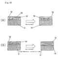
- a method for removing the impurities for example in the case of a gate insulating film in a MIS transistor, typically, a high-k film 52 having been formed on the upper surface of a Si substrate 51 is heat treated, as shown on the right side of Fig. 10(A).
- This impurity removing method comprises a step of forming HfO 2 (hafnium oxide) film by CVD (Chemical Vapor Deposition) method in combination with a step of removing impurities by plasma oxidation.
- CVD Chemical Vapor Deposition
- This invention was made, taking note of the foregoing matters, and has an object to provide a method for forming an insulating film in a semiconductor device (hereinafter simply referred to as an insulating film forming method), capable of preventing as many impurities as possible, which cause deterioration in film quality, from existing in an insulating film in a semiconductor device.
- an insulating film forming method of the present invention is characterized in that a step of forming an insulating film so as to have a thickness in the range of 0.3 to 2 nm and a step of removing impurities from the insulating film are repeated a plurality of times, to form an insulating film having a prescribed thickness (claim 1).
- an insulating film having a required thickness is not formed in a single process, but the step of forming an insulating film so as to have a thickness in the range of 0.3 to 2 nm and the step of removing impurities from the insulating film are repeated a plurality of times to form an insulating film having a prescribed thickness. In this manner, it is possible to easily and certainly form a high-k film containing as few impurities as possible, while preventing inconvenience caused by the growth of the interface layer.
- the step of removing impurities may be performed in a reducing gas atmosphere or an oxidizing gas atmosphere (claim 2), and further, the step of removing impurities may be performed in a reducing gas atmosphere combined with an oxidizing gas atmosphere (claim 3). It is possible to easily and certainly form a desired high-k film in any of the gas atmospheres.
- the reducing atmosphere in the step of removing impurities can be formed of any of single gases of an ammonia gas, a hydrogen gas and an inert gas, a mixed gas of these gases or plasma nitrogen, or formed in a vacuum (claim 4).
- the oxidizing gas atmosphere in the step of removing impurities can be formed of any of single gases of an oxygen gas, a nitrogen monoxide gas, a nitrous oxide gas and an ozone gas, a mixed gas of these gases or plasma oxygen (claim 5).
- Fig 1 is a view schematically showing a configuration of a MIS transistor 1 as a semiconductor device to which the insulating film forming method of the present invention is applied.
- reference numeral 2 denotes a Si monocrystal substrate (hereinafter simply referred to as a Si substrate), and the resistivity thereof is from 0.01 to 15 ⁇ ⁇ cm, for example.
- Reference numeral 3 denotes an element isolation oxide film for isolating elements, which is formed by thermal oxidation of the Si substrate 2.
- Reference numeral 4 denotes a gate insulating film to be formed on the surface 2a of the Si substrate 2. A method for forming the gate insulating film 4 is specifically described later.
- Reference numeral 5 denotes a gate electrode to be formed on the upper surface of the gate insulating film 4.
- the gate electrode 5 is made of a noble metal such as Pt (platinum) or a high melting point metal such as TiN or TaN, the noble metal and the high melting point metal not reacting with a polycrystal Si film, a polycrystal SiGe film or the gate insulating film 4.
- Reference numeral 6 denotes a channel region. P (phosphorous) or the like is injected into an n channel and B (boron) or the like is injected into a p channel, and those channels are heat treated at temperatures of 800 to 1,000 °C for 10 to 30 minutes to be activated.
- Reference numeral 7 denotes an interlayer insulating film, which for example comprises SiO 2 or the like and is formed by CVD (Chemical Vapor Deposition) method or the like.
- Reference numeral 8 denotes an extraction electrode of the channel 6.
- the extraction electrode 8 for example comprises Al and serves as a source/drain electrode. It is to be noted that patterning is performed for example by means of the photolithography technique.
- the gate insulating film 4 is made of a high-k film having a required thickness. As shown in Fig. 6, the gate insulating film 4 is characterized in that it is formed by sequentially repeating a film formation step 11 and an impurity removing step (anneal step) 12 a plurality of times. Namely, it is characterized in that, instead of forming the high-k film 4 having a required thickness on a Si substrate in a single process, a film having a prescribed thickness is formed by degrees and then annealed in an atmosphere of a prescribed gas to reduce as many residual impurities as possible. Therefore, before concrete examples of the method for forming the gate insulating film 4 are described, experiments conducted by the present inventors and consideration of the results thereof are described with reference to Figs. 2 to 5.
- an Al 2 O 3 film was formed by the ALD method so as to have a thickness of 0.3 to 6.3 nm.
- the film was formed under conditions that a substrate temperature was 250 °C and as precursor, TMA (Al(CH 3 ) 3 : trimethyl aluminum) was used as an Al precursor while a water vapor gas was used as an oxidant.
- TMA Al(CH 3 ) 3 : trimethyl aluminum
- the Al 2 O 3 film was analyzed using a TDS (Thermal Desorption Spectroscopy) device.
- Fig. 2 shows the results of the analyses. In Fig.
- TDS is a method of increasing a gas temperature and simultaneously analyzing a gas being desorbed
- performing TDS can be considered as being equivalent to performing heat treatment. From the results of this analysis, it was discovered that the thickness of the film from which impurities can be removed by heat treatment is limited to about 1.5 nm or smaller, and impurities may remain in a film having a thickness exceeding this limitation.
- an HfO 2 film was formed by the ALD method so as to have a thickness of 0.7 to 7.5 nm.
- the film was formed under conditions that a substrate temperature was 250 °C and as the precursor, TDMAH (Hf(N(CH 3 ) 2 ) 4 : tetrakis(dimethylamino) hafnium) was used as an Hf precursor while the water vapor gas was used as the oxidant.
- TDMAH Hf(N(CH 3 ) 2 ) 4 : tetrakis(dimethylamino) hafnium
- the HfO 2 film was subjected to TDS using the TDS device.
- Fig. 3 shows the results of the analysis.
- an HfAlO x film was formed by the ALD method so as to have a thickness of 0.7 to 11 nm.
- the film was formed under conditions that a substrate temperature was 250 °C and as the precursor, TMA was used as an Al precursor and TDMAH was used as the Hf precursor while the water vapor gas was used as the oxidant.
- the HfAlO x film was subjected to TDS using the TDS device.
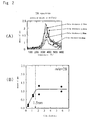
- Fig. 4 shows the results of the analysis. In Fig. 4, (A) shows a TDS spectrum with a molecular weight of 28 (C 2 H 4 ) when the film thickness is variously changed, and (B) shows the relation between the film thickness and the amount of the C 2 H 4 gas desorbed.
- the thickness of the film from which impurities can be removed changes depending upon the kind of element to constitute the film, and that the impurities can be certainly removed by heat treatment when the film thickness is in the range of 0.3 to 2.0 nm (optimally in the range of 0.5 to 1.8 nm). It should be noted that 0.3 nm is a minimum film thickness for forming a film, and it corresponds to a thickness of one monolayer (monoatomic layer).
- This impurity removing step is to anneal a high-k film in an atmosphere of a certain gas in a prescribed temperature condition.
- a reducing gas atmosphere or an oxidizing gas atmosphere can be employed.
- the impurity removing step is performed in the reducing gas atmosphere appropriately combined with the oxidizing gas atmosphere.
- Fig. 5 shows data of measurement by XPS (soft X-ray Photoelectron Spectroscopy) after the impurity removing step (anneal step).
- FIG. 5 (A) shows the case of performing a first anneal in the reducing gas atmosphere, and (B) shows the case of performing a first anneal in the oxidizing gas atmosphere.
- Fig. 5 reveals that the interface layer increases in a smaller degree when the anneal is performed in the reducing gas atmosphere rather than in the oxidizing gas atmosphere. That is, appropriate control of the atmosphere gas during the anneal can suppress the formation of the interface layer.
- a high-k film as the gate insulating film 4 has a film thickness of 4.0 nm.
- a Si substrate 2 made of a Si monocrystal plate having an appropriate thickness e.g. about 500 ⁇ m
- an HfAlO x film, as the high-k film, having a film thickness of 0.5 nm is formed (first film formation, c.f. reference numeral 11 in Fig. 6).
- the film is formed under conditions that a substrate temperature is 250 °C and as precursor, TMA is used as an Al precursor and TDMAH as an Hf precursor, while a water vapor gas as an oxidant.
- the HfAlO x film is heat treated in an NH 3 (ammonia) gas atmosphere as the reducing gas atmosphere at 650 °C for 30 seconds, to treat impurities (first heat treatment, c.f. reference numeral 12 in Fig. 6). It is preferable to perform this first heat treatment in the reducing gas atmosphere. This is because, since the film thickness becomes as thin as 0.5 nm if the heat treatment is performed in the oxidizing gas atmosphere, Si on the interface is oxidized to form SiO 2 , thereby forming an interface layer having a low dielectric constant. It is to be noted that, although the heat treatment is performed at a temperature of 650°C in the present example, it is found possible from the results shown in Fig.
- an HfAlO x film is formed so as to have the same thickness under the same film formation conditions as in the case of the first film formation. (second film formation, c.f. reference numeral 11 in Fig. 6).
- heat treatment is performed in an oxygen gas atmosphere (e.g. under a pressure of 130 Pa) at the same temperature for the same period of time as in the case of first heat treatment (second heat treatment, c.f. reference numeral 12 in Fig. 6).
- oxygen gas atmosphere e.g. under a pressure of 130 Pa
- the film formation and the heat treatment are alternately repeated until the seventh film formation and the seventh heat treatment are completed.
- the heat treatment is performed in the same manner as in the second heat treatment.
- the eighth film formation is performed in the same manner as in the first to seventh film formations, whereafter the impurities are treated by heat treatment in the oxygen gas atmosphere (oxidizing gas atmosphere) at the same temperature and for the same period of time as in the case of the first to seventh heat treatments, to treat the impurities.
- the oxygen gas atmosphere oxygen gas atmosphere
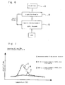
- Fig. 7 shows the results of TDS of the following three kinds of films: an HfAlO x film A (film thickness: 4.0 nm) formed by alternately repeating the foregoing film formation and heat treatment a plurality of times; an HfAlO. film B obtained by first forming an HfAlO x film having a thickness of 4.0 nm and finally heat treating the film at 650 °C for 30 seconds for treating impurities; and an HfAlO x film C obtained by first forming an HfAlO x film having a film thickness of 4.0 nm and finally heat treating the film at 850°C for 30 seconds for treating impurities.
- an HfAlO x film A film thickness: 4.0 nm
- an HfAlO. film B obtained by first forming an HfAlO x film having a thickness of 4.0 nm and finally heat treating the film at 650 °C for 30 seconds for treating impurities
- the HfAlO x film (high-k film) according to the method of the present invention contains few impurities, and there is no low dielectric constant layer between the HfAlO x film and Si. Further, in the method of the present invention, since the impurities can be removed at a relatively low temperature of 650 °C , crystallization of the high-k film is favorably suppressed, thereby eliminating disadvantages of crystallization of the high-k film, i.e. once crystallized, the high-k film has a crystal grain boundary as a point of weakness, resulting in decreased reliability.
- Fig. 8 shows a second example of the present invention.
- an HfAlO x film having a thickness of 3 nm is formed on the Si substrate.
- samples A, B and C are high-k films each formed by the steps (1) to (7) where an HfAlO x film having a thickness of 1 nm is formed and then heat treated in a prescribed gas atmosphere.
- a high-k film having a thickness of 3 nm formed in a single process according to the conventional method is referred to as a sample D. Any of these samples A to D was annealed in the oxygen gas atmosphere at 650°C as heat treatment (PDA) after the film formation.
- PDA heat treatment
- the samples A and B are in an ammonia gas atmosphere in a first anneal (heat treatment) whereas the sample C is annealed in the oxygen gas atmosphere in the first anneal (heat treatment).
- the samples A is annealed in the ammonia gas atmosphere whereas the sample B is annealed in the oxygen gas atmosphere.
- the sample C is annealed in the oxygen gas atmosphere in the first through third anneals (heat treatments)
- any of the samples A to C according to the method of the present invention is more excellent in electric characteristic than the sample D according to the conventional method. Namely, the smaller a hysteresis in a CV curve of a film, the lower the interface level of the film and the better quality the film has.
- the hysteresis of each of the samples A to C is significantly smaller than that of Sample D.
- the leak current of each of the samples A to C is significantly smaller than that of the sample D. This is because, as apparent from Fig. 1, each of the samples A to C is a dense film of good quality having a large film density and containing a very small amount of impurities as compared with the sample D. It is therefore found that the high-k film according to the method of the present invention has highly excellent properties as compared to the high-k film according to the conventional method.
- the reducing gas atmosphere or the oxidizing gas atmosphere was employed as the gas atmosphere in the impurity removing step (heat treatment or anneal step), and the ammonia gas was used as the reducing gas atmosphere while the oxygen gas was used as the oxidizing gas atmosphere.
- the present invention is not limited to those gases and various kinds of gases can be employed.
- the reducing gas atmosphere in the impurity removing step may be formed by the use of a hydrogen gas or an inert gas, by the use of a mixed gas of the ammonia gas, the hydrogen gas or the inert gas, or by the use of plasma nitrogen, or may further be formed in a vacuum.
- the oxidizing gas atmosphere in the impurity removing step may be formed by the use of a nitrous oxide (NO), a nitrogen monoxide (N 2 O) gas, or an ozone gas, or by the use of a mixed gas obtained by appropriately mixing these gases, or further by the use of plasma oxygen.
- NO nitrous oxide
- N 2 O nitrogen monoxide
- ozone gas a mixed gas obtained by appropriately mixing these gases, or further by the use of plasma oxygen.
- any of the foregoing embodiments was application of the method of the present invention to the method for forming the gate insulating film 4 of the MIS transistor 1, and the method for forming the gate insulating film 4 made of a high-k film on the Si substrate 2.
- the present invention is not limited to this method, and can be applied to formation of a capacitor insulating film of an MIM capacitor.
- Fig. 9 is a view schematically showing a configuration of an MIM capacitor 21.
- reference numeral 22 denotes a Si monocrystal substrate (hereinafter simply referred to as a Si substrate), and the resistivity thereof is from 0.01 to 15 ⁇ ⁇ cm, for example.
- Reference numeral 23 denotes an element isolation oxide film for isolating elements, which is formed by thermal oxidation of the Si substrate 2.
- Reference numeral 24 denotes a gate insulating film to be formed on the surface 22a of the Si substrate 22. The gate insulating film 24 is formed in the same manner as the formation of the gate insulating film 4 shown in the above-mentioned Fig. 1.
- Reference numeral 45 denotes a gate electrode to be formed on the upper surface of the gate insulating film 4.
- the gate electrode is made of a noble metal such as Pt (platinum) or a high melting point metal such as TiN or TaN, the noble metal and the high melting point metal not reacting with a polycrystal Si film, a polycrystal SiGe film or the gate insulating film 4.
- Reference numeral 46 denotes a channel region. P (phosphorous) or the like is injected into an n channel and B (boron) or the like is injected into a p channel, and those channels are heat treated at temperatures of 800 to 1,000 °C for 10 to 30 minutes to be activated.
- Reference numeral 27 denotes a first interlayer insulating film, which for example comprises SiO 2 or the like and formed by CVD method or the like.
- Reference numeral 28 denotes an extraction electrode of the channel 46.
- the extraction electrode 28 is formed in such a manner that a contact hole is formed in the first interlayer insulating film 27 by means of RIE (reactive ion etching) or the like, and a high melting point metal, such as Cu, Al, AlSi, Pt 2 Si, TiN or TaN, is then provided in the contact hole.
- RIE reactive ion etching
- Reference numeral 29 denotes a second interlayer insulating film to be formed on the upper surface of the first interlayer insulating film 27.
- the second interlayer insulating film 29 for example comprises SiO 2 , and formed by CVD method or the like.
- Reference numeral 30 denotes an extraction electrode to be provided in the second interlayer insulating film 29 so as to be electrically connected with one of the extraction electrode 28 to be formed in the first interlayer insulating film 27, and is formed in the same manner as the formation of the extraction electrode 28.
- Reference numeral 31 denotes a capacitor to be provided in the second interlayer insulating film 29 so as to be electrically connected with the other extraction electrode 28 to be formed in the first interlayer insulating film 27, and is constituted as described below. Namely, a contact hole is formed in the second interlayer insulating film 29, and a lower electrode 32, an upper electrode 33 and a capacitor insulating film 34 to be formed between the two electrodes 32 and 33 are formed in the contact hole, and constitute the capacitor 31.
- the lower electrode 32 comprises a noble metal such as Pt or a high melting point metal such as TiN or TaN.
- the upper electrode 33 comprises a noble metal such as Cu, Al or Pt or a high melting point metal such as TiN or TaN.
- Either the electrode 32 or 33 is constituted of a material that does not react with the capacitor insulating film 34.
- the capacitor insulating film 34 is then formed using a high-k film on the upper surface of the lower electrode 32. It is to be noted that patterning is performed for example by means of the photolithography technique.
- a SiO 2 film having a thickness of 200 nm was formed on the Si substrate, and on the upper surface thereof, a Pt film having a thickness of about 100 nm was formed, to give a lower capacity electrode.
- samples A to C were formed on the upper surface of the lower capacity electrode made of the Pt film, by the method shown in Fig. 8.
- a high-k film having a thickness of 3 nm was formed in a single process by the conventional method, and referred to as a sample D.
- a TiN film was then formed as an upper electrode.
- the electric characteristics of the capacitor insulating film were evaluated, to obtain the results shown in Table 3.
- dielectric breakdown voltage (MV/cm) A 8.0 ⁇ 10 B 8.4 ⁇ 10 C 8.6 ⁇ 12 D 3.5 ⁇ 7.4
- each of the samples A to C according to the method of the present invention is higher than that of the sample D according to the conventional method, and hence the samples A to C are films of good quality.
- each of the samples A to C is a dense film of good quality having a large film density and containing a very small amount of impurities as compared with the sample D. It is therefore found that the high-k film according to the method of the present invention also has highly excellent properties as the capacitor insulating film 34.
- the substrate was used as the substrate on which the high-k film was to be formed in the above-mentioned embodiments, the substrate is not limited thereto, and a GaAs compound semiconductor substrate or a SOI (Silicon On Insulator) substrate may be used as the substrate.
- a GaAs compound semiconductor substrate or a SOI (Silicon On Insulator) substrate may be used as the substrate.
- a gate insulating film made of a high-k film containing few impurities so as to reduce flat band shift and an interface fixed charge due to the impurities, resulting in production of a high-quality MIS transistor. It is also possible to form a capacitor insulating film made of a high-k film containing few impurities, so as to prevent a decrease in dielectric break down voltage due to the impurities, resulting in production of a high-quality MIM capacitor.
Landscapes
- Chemical & Material Sciences (AREA)
- General Chemical & Material Sciences (AREA)
- Chemical Kinetics & Catalysis (AREA)
- Engineering & Computer Science (AREA)
- Materials Engineering (AREA)
- Mechanical Engineering (AREA)
- Metallurgy (AREA)
- Organic Chemistry (AREA)
- Insulated Gate Type Field-Effect Transistor (AREA)
- Formation Of Insulating Films (AREA)
- Semiconductor Integrated Circuits (AREA)
- Thin Film Transistor (AREA)
Abstract
Description
| amount of carbon | denseness of film(g/cm3) | |
| A | 0.15 | 8.8 |
| B | 0.12 | 8.5 |
| C | 0.11 | 8.5 |
| D | 1.00 | 8.0 |
| hysteresis in.a CV (mV) | leak current (mV/cm2) | |
| A | 15 | 7.0 |
| B | 15 | 5.0 |
| | 10 | 1.1 |
| D | 80 | 11.0 |
| dielectric breakdown voltage (MV/cm) | |
| A | 8.0 ~ 10 |
| B | 8.4 ~ 10 |
| C | 8.6 ~ 12 |
| D | 3.5 ~ 7.4 |
Claims (5)
- A method for forming an insulating film in a semiconductor device characterized in that a step of forming an insulating film so as to have a thickness in the range of 0.3 to 2 nm and a step of removing impurities from the insulating film are repeated a plurality of times, to form an insulating film having a prescribed thickness.
- The method for forming an insulating film in a semiconductor device as claimed 1, therein the step of removing impurities is performed in a reducing gas atmosphere or an oxidizing gas atmosphere.
- The method for forming an insulating film in a semiconductor device as claimed 1, therein the step of removing impurities is performed in a reducing gas atmosphere combined with an oxidizing gas atmosphere.
- The method for forming an insulating film in a semiconductor device as claimed 2 or 3, therein the reducing atmosphere in the step of removing impurities is formed of any of single gases of an ammonia gas, a hydrogen gas and an inert gas, a mixed gas of these gases or plasma nitrogen, or formed in a vacuum.
- The method for forming an insulating film in a semiconductor device as claimed 2 or 3, therein the oxidizing gas atmosphere in the step of removing impurities is formed of any of single gases of an oxygen gas, a nitrogen monoxide gas, a nitrous oxide gas and an ozone gas, a mixed gas of these gases or plasma oxygen.
Applications Claiming Priority (3)
| Application Number | Priority Date | Filing Date | Title |
|---|---|---|---|
| JP2003079279A JP4140767B2 (en) | 2003-03-24 | 2003-03-24 | Method for forming insulating film in semiconductor device |
| JP2003079279 | 2003-03-24 | ||
| PCT/JP2004/003638 WO2004086485A1 (en) | 2003-03-24 | 2004-03-18 | Method for forming insulating film in semiconductor device |
Publications (4)
| Publication Number | Publication Date |
|---|---|
| EP1608007A1 true EP1608007A1 (en) | 2005-12-21 |
| EP1608007A4 EP1608007A4 (en) | 2010-03-17 |
| EP1608007B1 EP1608007B1 (en) | 2012-08-15 |
| EP1608007B8 EP1608007B8 (en) | 2012-09-26 |
Family
ID=33094838
Family Applications (1)
| Application Number | Title | Priority Date | Filing Date |
|---|---|---|---|
| EP04721668A Expired - Lifetime EP1608007B8 (en) | 2003-03-24 | 2004-03-18 | Method for forming insulating film in semiconductor device |
Country Status (6)
| Country | Link |
|---|---|
| US (1) | US20070077776A1 (en) |
| EP (1) | EP1608007B8 (en) |
| JP (1) | JP4140767B2 (en) |
| KR (1) | KR100751659B1 (en) |
| TW (1) | TWI348184B (en) |
| WO (1) | WO2004086485A1 (en) |
Families Citing this family (7)
| Publication number | Priority date | Publication date | Assignee | Title |
|---|---|---|---|---|
| US20050170665A1 (en) * | 2003-04-17 | 2005-08-04 | Fujitsu Limited | Method of forming a high dielectric film |
| KR100762896B1 (en) * | 2006-05-30 | 2007-10-08 | 주식회사 하이닉스반도체 | Thin film deposition method of semiconductor device |
| JP2010278319A (en) * | 2009-05-29 | 2010-12-09 | Renesas Electronics Corp | Semiconductor device and manufacturing method thereof |
| JP2012104569A (en) * | 2010-11-08 | 2012-05-31 | Hitachi Kokusai Electric Inc | Manufacturing method of semiconductor device and substrate processing apparatus |
| JP6540571B2 (en) | 2016-03-24 | 2019-07-10 | 豊田合成株式会社 | Semiconductor device manufacturing method and semiconductor device |
| JP6951548B2 (en) * | 2017-08-01 | 2021-10-20 | アプライド マテリアルズ インコーポレイテッドApplied Materials,Incorporated | Method of post-treatment of metal oxides |
| KR102563298B1 (en) | 2021-01-18 | 2023-08-03 | 주식회사 유진테크 | Method for removing impurities in thin film and substrate processing apparatus |
Family Cites Families (14)
| Publication number | Priority date | Publication date | Assignee | Title |
|---|---|---|---|---|
| US5338362A (en) * | 1992-08-29 | 1994-08-16 | Tokyo Electron Limited | Apparatus for processing semiconductor wafer comprising continuously rotating wafer table and plural chamber compartments |
| US6228751B1 (en) * | 1995-09-08 | 2001-05-08 | Semiconductor Energy Laboratory Co., Ltd. | Method of manufacturing a semiconductor device |
| US6228781B1 (en) * | 1997-04-02 | 2001-05-08 | Applied Materials, Inc. | Sequential in-situ heating and deposition of halogen-doped silicon oxide |
| US20040053472A1 (en) * | 2000-09-18 | 2004-03-18 | Hideki Kiryu | Method for film formation of gate insulator, apparatus for film formation of gate insulator, and cluster tool |
| KR100384850B1 (en) * | 2000-12-14 | 2003-05-22 | 주식회사 하이닉스반도체 | Method for forming Ta2O5 dielectric layer |
| US7037574B2 (en) | 2001-05-23 | 2006-05-02 | Veeco Instruments, Inc. | Atomic layer deposition for fabricating thin films |
| JP2002367990A (en) * | 2001-06-04 | 2002-12-20 | Tokyo Electron Ltd | Method for manufacturing semiconductor device |
| JP4416354B2 (en) * | 2001-06-29 | 2010-02-17 | 株式会社ルネサステクノロジ | Semiconductor device manufacturing method and manufacturing apparatus thereof |
| US20030198754A1 (en) * | 2001-07-16 | 2003-10-23 | Ming Xi | Aluminum oxide chamber and process |
| JP3941099B2 (en) * | 2001-12-19 | 2007-07-04 | ソニー株式会社 | Thin film formation method |
| JP4090347B2 (en) * | 2002-03-18 | 2008-05-28 | 株式会社日立国際電気 | Semiconductor device manufacturing method and substrate processing apparatus |
| US7160577B2 (en) * | 2002-05-02 | 2007-01-09 | Micron Technology, Inc. | Methods for atomic-layer deposition of aluminum oxides in integrated circuits |
| US7442415B2 (en) * | 2003-04-11 | 2008-10-28 | Sharp Laboratories Of America, Inc. | Modulated temperature method of atomic layer deposition (ALD) of high dielectric constant films |
| US7351626B2 (en) * | 2003-12-18 | 2008-04-01 | Texas Instruments Incorporated | Method for controlling defects in gate dielectrics |
-
2003
- 2003-03-24 JP JP2003079279A patent/JP4140767B2/en not_active Expired - Fee Related
-
2004
- 2004-03-18 EP EP04721668A patent/EP1608007B8/en not_active Expired - Lifetime
- 2004-03-18 KR KR1020057017077A patent/KR100751659B1/en not_active Expired - Fee Related
- 2004-03-18 US US10/550,805 patent/US20070077776A1/en not_active Abandoned
- 2004-03-18 WO PCT/JP2004/003638 patent/WO2004086485A1/en not_active Ceased
- 2004-03-19 TW TW093107466A patent/TWI348184B/en not_active IP Right Cessation
Also Published As
| Publication number | Publication date |
|---|---|
| TWI348184B (en) | 2011-09-01 |
| JP2004288884A (en) | 2004-10-14 |
| KR100751659B1 (en) | 2007-08-23 |
| JP4140767B2 (en) | 2008-08-27 |
| TW200423238A (en) | 2004-11-01 |
| EP1608007B1 (en) | 2012-08-15 |
| KR20050115910A (en) | 2005-12-08 |
| WO2004086485A1 (en) | 2004-10-07 |
| EP1608007A4 (en) | 2010-03-17 |
| US20070077776A1 (en) | 2007-04-05 |
| EP1608007B8 (en) | 2012-09-26 |
Similar Documents
| Publication | Publication Date | Title |
|---|---|---|
| JP4047075B2 (en) | Semiconductor device | |
| US6642131B2 (en) | Method of forming a silicon-containing metal-oxide gate dielectric by depositing a high dielectric constant film on a silicon substrate and diffusing silicon from the substrate into the high dielectric constant film | |
| KR100563748B1 (en) | Manufacturing method of semiconductor device | |
| JP4340830B2 (en) | Method for forming gate insulating film of semiconductor device | |
| US6911707B2 (en) | Ultrathin high-K gate dielectric with favorable interface properties for improved semiconductor device performance | |
| EP1463121B1 (en) | Semiconductor device and production method therefor | |
| US8748992B2 (en) | MOS transistors including SiON gate dielectric with enhanced nitrogen concentration at its sidewalls | |
| US7737511B2 (en) | Semiconductor device and method of manufacturing the same | |
| US20050280105A1 (en) | Method of forming metal/high-k gate stacks with high mobility | |
| US20030155582A1 (en) | Gate dielectric structures for integrated circuits and methods for making and using such gate dielectric structures | |
| WO2007118031A2 (en) | Silicon oxynitride gate dielectric formation using multiple annealing steps | |
| US20050282400A1 (en) | Method of forming a dielectric film | |
| US20100320520A1 (en) | Dielectric, capacitor using dielectric, semiconductor device using dielectric, and manufacturing method of dielectric | |
| CN101471254A (en) | Method for forming dielectric films | |
| US6866890B2 (en) | Method of forming a dielectric film | |
| JP7056232B2 (en) | Silicon Carbide Semiconductor Device and Method for Manufacturing Silicon Carbide Semiconductor Device | |
| JP2005510872A (en) | Method for forming an oxynitride spacer for a metal gate electrode using a PECVD process in a silicon-deficient atmosphere | |
| EP1608007B1 (en) | Method for forming insulating film in semiconductor device | |
| EP1363333A1 (en) | Semiconductor device and its manufacturing method | |
| WO2004107451A1 (en) | Semiconductor device fitted with mis type field-effect transistor, process for producing the same and method of forming metal oxide film | |
| US20070287199A1 (en) | Base oxide engineering for high-K gate stacks | |
| US20070166931A1 (en) | Methods of Manufacturing A Semiconductor Device for Improving the Electrical Characteristics of A Dielectric Film |
Legal Events
| Date | Code | Title | Description |
|---|---|---|---|
| PUAI | Public reference made under article 153(3) epc to a published international application that has entered the european phase |
Free format text: ORIGINAL CODE: 0009012 |
|
| 17P | Request for examination filed |
Effective date: 20050930 |
|
| AK | Designated contracting states |
Kind code of ref document: A1 Designated state(s): AT BE BG CH CY CZ DE DK EE ES FI FR GB GR HU IE IT LI LU MC NL PL PT RO SE SI SK TR |
|
| AX | Request for extension of the european patent |
Extension state: AL LT LV MK |
|
| DAX | Request for extension of the european patent (deleted) | ||
| RBV | Designated contracting states (corrected) |
Designated state(s): BE DE FI FR |
|
| RAP1 | Party data changed (applicant data changed or rights of an application transferred) |
Owner name: ROHM CO., LTD. Owner name: RENESAS TECHNOLOGY CORP. Owner name: HORIBA, LTD. |
|
| A4 | Supplementary search report drawn up and despatched |
Effective date: 20100216 |
|
| RIC1 | Information provided on ipc code assigned before grant |
Ipc: H01L 21/316 20060101AFI20041014BHEP Ipc: H01L 21/318 20060101ALI20100210BHEP Ipc: C23C 16/455 20060101ALI20100210BHEP Ipc: C23C 16/56 20060101ALI20100210BHEP |
|
| 17Q | First examination report despatched |
Effective date: 20110317 |
|
| GRAP | Despatch of communication of intention to grant a patent |
Free format text: ORIGINAL CODE: EPIDOSNIGR1 |
|
| RIC1 | Information provided on ipc code assigned before grant |
Ipc: H01L 21/314 20060101ALI20120202BHEP Ipc: C23C 16/56 20060101ALI20120202BHEP Ipc: H01L 21/28 20060101ALI20120202BHEP Ipc: H01L 21/318 20060101ALI20120202BHEP Ipc: C23C 16/455 20060101ALI20120202BHEP Ipc: H01L 21/3105 20060101ALI20120202BHEP Ipc: H01L 29/51 20060101ALI20120202BHEP Ipc: H01L 21/316 20060101AFI20120202BHEP |
|
| GRAS | Grant fee paid |
Free format text: ORIGINAL CODE: EPIDOSNIGR3 |
|
| GRAA | (expected) grant |
Free format text: ORIGINAL CODE: 0009210 |
|
| AK | Designated contracting states |
Kind code of ref document: B1 Designated state(s): BE DE FI FR |
|
| RAP2 | Party data changed (patent owner data changed or rights of a patent transferred) |
Owner name: RENESAS ELECTRONICS CORPORATION Owner name: HORIBA, LTD. Owner name: ROHM CO., LTD. |
|
| REG | Reference to a national code |
Ref country code: DE Ref legal event code: R082 Ref document number: 602004038921 Country of ref document: DE Representative=s name: BEETZ & PARTNER PATENT- UND RECHTSANWAELTE, DE Ref country code: DE Ref legal event code: R082 Ref document number: 602004038921 Country of ref document: DE Representative=s name: BEETZ & PARTNER MBB, DE Ref country code: DE Ref legal event code: R082 Ref document number: 602004038921 Country of ref document: DE Representative=s name: BEETZ & PARTNER MBB PATENT- UND RECHTSANWAELTE, DE |
|
| REG | Reference to a national code |
Ref country code: DE Ref legal event code: R096 Ref document number: 602004038921 Country of ref document: DE Effective date: 20121011 |
|
| REG | Reference to a national code |
Ref country code: DE Ref legal event code: R082 Ref document number: 602004038921 Country of ref document: DE Representative=s name: BEETZ & PARTNER PATENT- UND RECHTSANWAELTE, DE Ref country code: DE Ref legal event code: R082 Ref document number: 602004038921 Country of ref document: DE Representative=s name: BEETZ & PARTNER MBB, DE Ref country code: DE Ref legal event code: R082 Ref document number: 602004038921 Country of ref document: DE Representative=s name: BEETZ & PARTNER MBB PATENT- UND RECHTSANWAELTE, DE |
|
| PG25 | Lapsed in a contracting state [announced via postgrant information from national office to epo] |
Ref country code: BE Free format text: LAPSE BECAUSE OF FAILURE TO SUBMIT A TRANSLATION OF THE DESCRIPTION OR TO PAY THE FEE WITHIN THE PRESCRIBED TIME-LIMIT Effective date: 20120815 |
|
| PGFP | Annual fee paid to national office [announced via postgrant information from national office to epo] |
Ref country code: FI Payment date: 20130314 Year of fee payment: 10 Ref country code: DE Payment date: 20130322 Year of fee payment: 10 |
|
| PLBE | No opposition filed within time limit |
Free format text: ORIGINAL CODE: 0009261 |
|
| STAA | Information on the status of an ep patent application or granted ep patent |
Free format text: STATUS: NO OPPOSITION FILED WITHIN TIME LIMIT |
|
| 26N | No opposition filed |
Effective date: 20130516 |
|
| REG | Reference to a national code |
Ref country code: DE Ref legal event code: R097 Ref document number: 602004038921 Country of ref document: DE Effective date: 20130516 |
|
| REG | Reference to a national code |
Ref country code: FR Ref legal event code: ST Effective date: 20131129 |
|
| PG25 | Lapsed in a contracting state [announced via postgrant information from national office to epo] |
Ref country code: FR Free format text: LAPSE BECAUSE OF NON-PAYMENT OF DUE FEES Effective date: 20130402 |
|
| REG | Reference to a national code |
Ref country code: DE Ref legal event code: R119 Ref document number: 602004038921 Country of ref document: DE |
|
| PG25 | Lapsed in a contracting state [announced via postgrant information from national office to epo] |
Ref country code: FI Free format text: LAPSE BECAUSE OF NON-PAYMENT OF DUE FEES Effective date: 20140318 |
|
| REG | Reference to a national code |
Ref country code: DE Ref legal event code: R119 Ref document number: 602004038921 Country of ref document: DE Effective date: 20141001 |
|
| PG25 | Lapsed in a contracting state [announced via postgrant information from national office to epo] |
Ref country code: DE Free format text: LAPSE BECAUSE OF NON-PAYMENT OF DUE FEES Effective date: 20141001 |