EP1607930A1 - Drive method for plasma display panel - Google Patents
Drive method for plasma display panel Download PDFInfo
- Publication number
- EP1607930A1 EP1607930A1 EP04722693A EP04722693A EP1607930A1 EP 1607930 A1 EP1607930 A1 EP 1607930A1 EP 04722693 A EP04722693 A EP 04722693A EP 04722693 A EP04722693 A EP 04722693A EP 1607930 A1 EP1607930 A1 EP 1607930A1
- Authority
- EP
- European Patent Office
- Prior art keywords
- discharge
- electrodes
- priming
- scan
- electrode
- Prior art date
- Legal status (The legal status is an assumption and is not a legal conclusion. Google has not performed a legal analysis and makes no representation as to the accuracy of the status listed.)
- Withdrawn
Links
Images


Classifications
-
- G—PHYSICS
- G09—EDUCATION; CRYPTOGRAPHY; DISPLAY; ADVERTISING; SEALS
- G09G—ARRANGEMENTS OR CIRCUITS FOR CONTROL OF INDICATING DEVICES USING STATIC MEANS TO PRESENT VARIABLE INFORMATION
- G09G3/00—Control arrangements or circuits, of interest only in connection with visual indicators other than cathode-ray tubes
- G09G3/20—Control arrangements or circuits, of interest only in connection with visual indicators other than cathode-ray tubes for presentation of an assembly of a number of characters, e.g. a page, by composing the assembly by combination of individual elements arranged in a matrix no fixed position being assigned to or needed to be assigned to the individual characters or partial characters
- G09G3/22—Control arrangements or circuits, of interest only in connection with visual indicators other than cathode-ray tubes for presentation of an assembly of a number of characters, e.g. a page, by composing the assembly by combination of individual elements arranged in a matrix no fixed position being assigned to or needed to be assigned to the individual characters or partial characters using controlled light sources
- G09G3/28—Control arrangements or circuits, of interest only in connection with visual indicators other than cathode-ray tubes for presentation of an assembly of a number of characters, e.g. a page, by composing the assembly by combination of individual elements arranged in a matrix no fixed position being assigned to or needed to be assigned to the individual characters or partial characters using controlled light sources using luminous gas-discharge panels, e.g. plasma panels
- G09G3/288—Control arrangements or circuits, of interest only in connection with visual indicators other than cathode-ray tubes for presentation of an assembly of a number of characters, e.g. a page, by composing the assembly by combination of individual elements arranged in a matrix no fixed position being assigned to or needed to be assigned to the individual characters or partial characters using controlled light sources using luminous gas-discharge panels, e.g. plasma panels using AC panels
- G09G3/291—Control arrangements or circuits, of interest only in connection with visual indicators other than cathode-ray tubes for presentation of an assembly of a number of characters, e.g. a page, by composing the assembly by combination of individual elements arranged in a matrix no fixed position being assigned to or needed to be assigned to the individual characters or partial characters using controlled light sources using luminous gas-discharge panels, e.g. plasma panels using AC panels controlling the gas discharge to control a cell condition, e.g. by means of specific pulse shapes
- G09G3/292—Control arrangements or circuits, of interest only in connection with visual indicators other than cathode-ray tubes for presentation of an assembly of a number of characters, e.g. a page, by composing the assembly by combination of individual elements arranged in a matrix no fixed position being assigned to or needed to be assigned to the individual characters or partial characters using controlled light sources using luminous gas-discharge panels, e.g. plasma panels using AC panels controlling the gas discharge to control a cell condition, e.g. by means of specific pulse shapes for reset discharge, priming discharge or erase discharge occurring in a phase other than addressing
-
- G—PHYSICS
- G09—EDUCATION; CRYPTOGRAPHY; DISPLAY; ADVERTISING; SEALS
- G09G—ARRANGEMENTS OR CIRCUITS FOR CONTROL OF INDICATING DEVICES USING STATIC MEANS TO PRESENT VARIABLE INFORMATION
- G09G3/00—Control arrangements or circuits, of interest only in connection with visual indicators other than cathode-ray tubes
- G09G3/20—Control arrangements or circuits, of interest only in connection with visual indicators other than cathode-ray tubes for presentation of an assembly of a number of characters, e.g. a page, by composing the assembly by combination of individual elements arranged in a matrix no fixed position being assigned to or needed to be assigned to the individual characters or partial characters
- G09G3/22—Control arrangements or circuits, of interest only in connection with visual indicators other than cathode-ray tubes for presentation of an assembly of a number of characters, e.g. a page, by composing the assembly by combination of individual elements arranged in a matrix no fixed position being assigned to or needed to be assigned to the individual characters or partial characters using controlled light sources
- G09G3/28—Control arrangements or circuits, of interest only in connection with visual indicators other than cathode-ray tubes for presentation of an assembly of a number of characters, e.g. a page, by composing the assembly by combination of individual elements arranged in a matrix no fixed position being assigned to or needed to be assigned to the individual characters or partial characters using controlled light sources using luminous gas-discharge panels, e.g. plasma panels
- G09G3/288—Control arrangements or circuits, of interest only in connection with visual indicators other than cathode-ray tubes for presentation of an assembly of a number of characters, e.g. a page, by composing the assembly by combination of individual elements arranged in a matrix no fixed position being assigned to or needed to be assigned to the individual characters or partial characters using controlled light sources using luminous gas-discharge panels, e.g. plasma panels using AC panels
- G09G3/291—Control arrangements or circuits, of interest only in connection with visual indicators other than cathode-ray tubes for presentation of an assembly of a number of characters, e.g. a page, by composing the assembly by combination of individual elements arranged in a matrix no fixed position being assigned to or needed to be assigned to the individual characters or partial characters using controlled light sources using luminous gas-discharge panels, e.g. plasma panels using AC panels controlling the gas discharge to control a cell condition, e.g. by means of specific pulse shapes
- G09G3/293—Control arrangements or circuits, of interest only in connection with visual indicators other than cathode-ray tubes for presentation of an assembly of a number of characters, e.g. a page, by composing the assembly by combination of individual elements arranged in a matrix no fixed position being assigned to or needed to be assigned to the individual characters or partial characters using controlled light sources using luminous gas-discharge panels, e.g. plasma panels using AC panels controlling the gas discharge to control a cell condition, e.g. by means of specific pulse shapes for address discharge
-
- G—PHYSICS
- G09—EDUCATION; CRYPTOGRAPHY; DISPLAY; ADVERTISING; SEALS
- G09G—ARRANGEMENTS OR CIRCUITS FOR CONTROL OF INDICATING DEVICES USING STATIC MEANS TO PRESENT VARIABLE INFORMATION
- G09G3/00—Control arrangements or circuits, of interest only in connection with visual indicators other than cathode-ray tubes
- G09G3/20—Control arrangements or circuits, of interest only in connection with visual indicators other than cathode-ray tubes for presentation of an assembly of a number of characters, e.g. a page, by composing the assembly by combination of individual elements arranged in a matrix no fixed position being assigned to or needed to be assigned to the individual characters or partial characters
- G09G3/22—Control arrangements or circuits, of interest only in connection with visual indicators other than cathode-ray tubes for presentation of an assembly of a number of characters, e.g. a page, by composing the assembly by combination of individual elements arranged in a matrix no fixed position being assigned to or needed to be assigned to the individual characters or partial characters using controlled light sources
- G09G3/28—Control arrangements or circuits, of interest only in connection with visual indicators other than cathode-ray tubes for presentation of an assembly of a number of characters, e.g. a page, by composing the assembly by combination of individual elements arranged in a matrix no fixed position being assigned to or needed to be assigned to the individual characters or partial characters using controlled light sources using luminous gas-discharge panels, e.g. plasma panels
- G09G3/288—Control arrangements or circuits, of interest only in connection with visual indicators other than cathode-ray tubes for presentation of an assembly of a number of characters, e.g. a page, by composing the assembly by combination of individual elements arranged in a matrix no fixed position being assigned to or needed to be assigned to the individual characters or partial characters using controlled light sources using luminous gas-discharge panels, e.g. plasma panels using AC panels
- G09G3/291—Control arrangements or circuits, of interest only in connection with visual indicators other than cathode-ray tubes for presentation of an assembly of a number of characters, e.g. a page, by composing the assembly by combination of individual elements arranged in a matrix no fixed position being assigned to or needed to be assigned to the individual characters or partial characters using controlled light sources using luminous gas-discharge panels, e.g. plasma panels using AC panels controlling the gas discharge to control a cell condition, e.g. by means of specific pulse shapes
- G09G3/294—Control arrangements or circuits, of interest only in connection with visual indicators other than cathode-ray tubes for presentation of an assembly of a number of characters, e.g. a page, by composing the assembly by combination of individual elements arranged in a matrix no fixed position being assigned to or needed to be assigned to the individual characters or partial characters using controlled light sources using luminous gas-discharge panels, e.g. plasma panels using AC panels controlling the gas discharge to control a cell condition, e.g. by means of specific pulse shapes for lighting or sustain discharge
- G09G3/2948—Control arrangements or circuits, of interest only in connection with visual indicators other than cathode-ray tubes for presentation of an assembly of a number of characters, e.g. a page, by composing the assembly by combination of individual elements arranged in a matrix no fixed position being assigned to or needed to be assigned to the individual characters or partial characters using controlled light sources using luminous gas-discharge panels, e.g. plasma panels using AC panels controlling the gas discharge to control a cell condition, e.g. by means of specific pulse shapes for lighting or sustain discharge by increasing the total sustaining time with respect to other times in the frame
-
- G—PHYSICS
- G09—EDUCATION; CRYPTOGRAPHY; DISPLAY; ADVERTISING; SEALS
- G09G—ARRANGEMENTS OR CIRCUITS FOR CONTROL OF INDICATING DEVICES USING STATIC MEANS TO PRESENT VARIABLE INFORMATION
- G09G3/00—Control arrangements or circuits, of interest only in connection with visual indicators other than cathode-ray tubes
- G09G3/20—Control arrangements or circuits, of interest only in connection with visual indicators other than cathode-ray tubes for presentation of an assembly of a number of characters, e.g. a page, by composing the assembly by combination of individual elements arranged in a matrix no fixed position being assigned to or needed to be assigned to the individual characters or partial characters
- G09G3/22—Control arrangements or circuits, of interest only in connection with visual indicators other than cathode-ray tubes for presentation of an assembly of a number of characters, e.g. a page, by composing the assembly by combination of individual elements arranged in a matrix no fixed position being assigned to or needed to be assigned to the individual characters or partial characters using controlled light sources
- G09G3/28—Control arrangements or circuits, of interest only in connection with visual indicators other than cathode-ray tubes for presentation of an assembly of a number of characters, e.g. a page, by composing the assembly by combination of individual elements arranged in a matrix no fixed position being assigned to or needed to be assigned to the individual characters or partial characters using controlled light sources using luminous gas-discharge panels, e.g. plasma panels
- G09G3/288—Control arrangements or circuits, of interest only in connection with visual indicators other than cathode-ray tubes for presentation of an assembly of a number of characters, e.g. a page, by composing the assembly by combination of individual elements arranged in a matrix no fixed position being assigned to or needed to be assigned to the individual characters or partial characters using controlled light sources using luminous gas-discharge panels, e.g. plasma panels using AC panels
- G09G3/298—Control arrangements or circuits, of interest only in connection with visual indicators other than cathode-ray tubes for presentation of an assembly of a number of characters, e.g. a page, by composing the assembly by combination of individual elements arranged in a matrix no fixed position being assigned to or needed to be assigned to the individual characters or partial characters using controlled light sources using luminous gas-discharge panels, e.g. plasma panels using AC panels using surface discharge panels
- G09G3/2983—Control arrangements or circuits, of interest only in connection with visual indicators other than cathode-ray tubes for presentation of an assembly of a number of characters, e.g. a page, by composing the assembly by combination of individual elements arranged in a matrix no fixed position being assigned to or needed to be assigned to the individual characters or partial characters using controlled light sources using luminous gas-discharge panels, e.g. plasma panels using AC panels using surface discharge panels using non-standard pixel electrode arrangements
- G09G3/2986—Control arrangements or circuits, of interest only in connection with visual indicators other than cathode-ray tubes for presentation of an assembly of a number of characters, e.g. a page, by composing the assembly by combination of individual elements arranged in a matrix no fixed position being assigned to or needed to be assigned to the individual characters or partial characters using controlled light sources using luminous gas-discharge panels, e.g. plasma panels using AC panels using surface discharge panels using non-standard pixel electrode arrangements with more than 3 electrodes involved in the operation
-
- H—ELECTRICITY
- H01—ELECTRIC ELEMENTS
- H01J—ELECTRIC DISCHARGE TUBES OR DISCHARGE LAMPS
- H01J11/00—Gas-filled discharge tubes with alternating current induction of the discharge, e.g. alternating current plasma display panels [AC-PDP]; Gas-filled discharge tubes without any main electrode inside the vessel; Gas-filled discharge tubes with at least one main electrode outside the vessel
- H01J11/20—Constructional details
- H01J11/22—Electrodes, e.g. special shape, material or configuration
Definitions
- the present invention relates to a method of driving a plasma display panel.
- a plasma display panel (hereinafter abbreviated as a PDP or a panel) is a display device having excellent visibility and featuring a large screen, thinness and light weight.
- the systems of discharging a PDP include an alternating-current (AC) type and direct-current (DC) type.
- the electrode structures thereof include a three-electrode surface-discharge type and an opposite-discharge type.
- the current mainstream is an AC type three-electrode PDP, which is an AC surface-discharge type, because this type of PDP is suitable for higher definition and easy to manufacture.
- an AC type three-electrode PDP has a large number of discharge cells formed between a front panel and rear panel faced with each other.
- a plurality of display electrodes each made of a pair of scan electrode and sustain electrode, are formed on a front glass substrate in parallel with each other.
- a dielectric layer and a protective layer are formed to cover these display electrodes.
- a plurality of parallel data electrodes is formed on a rear glass substrate.
- a dielectric layer is formed on the data electrodes to cover them.
- a plurality of barrier ribs is formed on the dielectric layer in parallel with the data electrodes. Phosphor layers are formed on the surface of the dielectric layer and the side faces of the barrier ribs.
- the front panel and the rear panel are faced with each other and sealed together so that the display electrodes and data electrodes intersect with each other.
- a discharge gas is filled into an inside discharge space formed therebetween.
- ultraviolet light is generated by gas discharge in each discharge cell. This ultraviolet light excites respective phosphors to emit R, G, or B color, for color display.
- a general method of driving a panel is a so-called sub-field method: one field period is divided into a plurality of sub-fields and combination of light-emitting sub-fields provides gradation images for display. Now, each of the sub-fields has an initializing period, writing period, and sustaining period.
- scan pulses are sequentially applied to scan electrodes, and write pulses corresponding to the signals of an image to be displayed are applied to data electrodes.
- selective writing discharge is caused between scan electrodes and corresponding data electrodes for selective formation of wall electric charge.
- a predetermined number of sustain pulses are applied between scan electrodes and corresponding sustain electrodes. Then, the discharge cells in which wall electric charge are formed by the writing discharge are selectively discharged and light is emitted from the discharge cells.
- priming caused by discharge rapidly decreases as time elapses. This causes the following problems in the method of driving a panel described above.
- priming generated in the initializing discharge is insufficient.
- This insufficient priming causes a large discharge delay and unstable wiring operation, thus degrading the image display quality.
- the time taken for the writing period is too long.
- the present invention addresses these problems and aims to provide a method of driving a plasma display panel capable of performing stable and high-speed writing operation.
- the pulse width of scan pulses applied to scan electrodes in which writing operation is performed but no priming discharge is caused with the scanning of the scan electrodes is shorter than the pulse width of scan pulses applied to other scan electrodes in which writing operation is performed and priming discharge is caused with the scanning of the scan electrodes, in the writing period.
- Fig. 1 is a sectional view showing an example of a panel used for the exemplary embodiment of the present invention.
- Fig. 2 is a schematic perspective view showing the structure of the rear substrate side of the panel.
- front substrate 1 and rear substrate 2 both made of glass are faced with each other to sandwich a discharge space therebetween.
- a mixed gas of neon and xenon for radiating ultraviolet light by discharge is filled.
- a plurality of pairs of scan electrode 6 and sustain electrode 7 are formed in parallel with each other. Further, scan electrodes 6 and sustain electrodes 7 are alternately arranged in pairs like sustain electrode 7 - scan electrode 6 - scan electrode 6 - sustain electrode 7 - sustain electrode 7 - scan electrode 6, etc.
- Scan electrode 6 and sustain electrode 7 are made of transparent electrodes 6a and 7a, and metal buses 6b and 7b formed on transparent electrodes 6a and 7a, respectively.
- light-absorbing layers 8 each made of a black material, are provided.
- Projection 6b' of metal bus 6b in one of adjacent scan electrodes 6 projects onto light-absorbing layer 8.
- Dielectric layer 4 and protective layer 5 are formed to cover these scan electrodes 6, sustain electrodes 7, and light-absorbing layers 8.
- each barrier rib 10 is made of vertical walls 10a extending in parallel with data electrodes 9, and horizontal walls 10b for forming discharge cells 11 and forming clearance 13 between discharge cells 11.
- priming electrode 14 is formed in the direction orthogonal to data electrodes 9, to form priming cell 13a.
- priming electrodes 14 are not provided in all the clearances 13, and are formed in priming cells 13 in every other one of clearances 13.
- phosphor layers 12 are provided on the surface of dielectric layer 15 corresponding to discharge cells 11 and the side faces of barrier ribs 10. However, no phosphor layer 12 is formed on the side of clearances 13.
- each projection 6b' of metal bus 6b in scan electrode 6 formed on front substrate 1 that projects onto light-absorbing layer 8 is positioned in parallel with corresponding priming electrode 14 on rear substrate 2 and faced therewith in priming cell 13a.
- the panel shown in Figs. 1 and 2 is structured to include priming cells 13a, each for performing priming discharge between projection 6b' formed on the side of front substrate 1 and priming electrode 14 formed on the side of rear substrate 2.
- dielectric layer 16 is further formed to cover priming electrodes 14.
- the interval between projection 6b' in scan electrode 6 and corresponding priming electrode 14 is shorter than the interval between data electrode 9 and corresponding scan electrode 6.
- the discharge-starting voltage of the priming discharge is lower than that of the writing discharge, and the priming discharge is more likely to occur.
- Fig. 3 is a diagram showing an arrangement of electrodes in the panel used for the exemplary embodiment of the present invention.
- M columns of data electrodes D 1 to D m (data electrodes 9 in Fig. 1) are arranged in the column direction.
- N rows of scan electrodes SC 1 to SC n (scan electrodes 6 in Fig. 1), and n rows of sustain electrodes SU 1 to SU n (sustain electrodes 7 in Fig. 1) are alternately arranged in pairs in the row direction like sustain electrode SU 1 - scan electrode SC 1 - scan electrode SC 2 - sustain electrode SU 2 , etc.
- projections 6b' are provided only in odd-numbered scan electrodes SU 1 , SU 3 , etc.
- N/2 rows of priming electrodes PR 1 , PR 3 , etc. are arranged to be faced with the corresponding projections of these scan electrodes SU 1 , SU 3 , etc.
- odd-numbered scan electrodes SC p are scan electrodes with projections 6b' in which writing operation is performed and priming discharge is caused with the scanning of the scan electrodes.
- even-numbered scan electrodes SC p+1 are scan electrodes with no projections 6b in which writing operation is performed but no priming discharge is caused with the scanning of the scan electrodes.
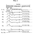
- Fig. 4 is a diagram showing a driving waveform in the method of driving the panel used for the exemplary embodiment of the present invention.
- one field period is made of a plurality of sub-fields, each including an initializing period, writing period, and sustaining period. Because the same operation is performed in each sub-field, except for the number of sustain pulses in the sustaining period, operation in one sub-filed is described hereinafter.
- each of data electrodes D 1 to D m , sustain electrode SU 1 to SU n , and priming electrodes PR 1 to PR n-1 is held at 0 (V).
- Applied to each of scan electrodes SC 1 to SC n is a ramp waveform voltage gradually increasing from a voltage of V i1 not larger than discharge-starting voltage across the scan electrodes and sustain electrodes SU 1 to SU n to a voltage of V i2 exceeding the discharge-starting voltage.
- first weak initializing discharge occurs between scan electrodes SC 1 to SC n , and sustain electrodes SU 1 to SU n , data electrodes D 1 to D m , and priming electrodes PR 1 to PR n-1 .
- negative wall voltage accumulates on scan electrodes SC 1 to SC n
- positive wall voltage accumulates on data electrodes D 1 to D m , sustain electrodes SU 1 to SU n , and priming electrodes PR 1 to PR n-1 .
- the wall voltage on the electrodes is the voltage generated by the wall charge accumulating on the dielectric layers covering the electrodes.
- each of sustain electrode SU 1 to SU n is held at a positive voltage of Ve.
- Applied to each of scan electrodes SC 1 to SC n is a ramp waveform voltage gradually decreasing from a voltage of V i3 not larger than discharge-starting voltage across the scan electrodes and sustain electrodes SU 1 to SU n to a voltage of V i4 exceeding the discharge-starting voltage.
- second weak initializing discharge occurs between scan electrodes SC 1 to SC n , and sustain electrodes SU 1 to SU n , data electrodes D 1 to D m , and priming electrodes PR 1 to PR n-1 .
- the negative wall voltage on scan electrodes SC 1 to SC n and the positive wall voltage on sustain electrodes SU 1 to SU n are weakened.
- the positive wall voltage on data electrodes D 1 to D m is adjusted to a value appropriate for writing operation.
- the positive wall voltage on priming electrodes PR 1 to PR n-1 is also adjusted to a value appropriate for priming operation.
- scan pulse Va is applied to scan electrode SC 1 of the first row.
- priming discharge occurs between priming electrode PR 1 and projection 6b' in scan electrode SC 1 .
- the priming diffuses inside of discharge cells C 1,1 to C 1, m in the first row corresponding to scan electrode SC 1 of the first row and discharge cells C 2,1 to C 2,m in the second row corresponding to scan electrode SC 2 of the second row. Because the priming cells are structured to easily discharge as described above, in this discharge, high-speed and stable priming discharge with a small discharge delay is obtained.
- positive write pulse voltage Vd is applied to data electrode D k (k being an integer ranging from 1 to m) corresponding to the signal of an image to be displayed in the first row, among data electrodes D 1 to D m .
- discharge occurs at the intersection of data electrode D k to which write pulse voltage Vd has been applied and scan electrode SC 1 .
- This discharge develops to the discharge between sustain electrode SU 1 and scan electrode SC 1 in corresponding discharge cell C 1,k .
- positive voltage accumulates on scan electrode SC 1 and negative voltage accumulates on sustain electrode SU 1 in discharge cell C 1,k .
- the pulse width of the scan pulse applied to scan electrode SC 1 of the first row is the sum of time tp necessary for the priming discharge and time tw necessary for the writing operation, i.e. tp + tw.
- scan electrode SC 1 of the first row is a scan electrode in which writing is performed and the priming discharge is caused with scanning of the scan electrode.
- the discharge in discharge cell C 1,k occurs with the priming supplied from the priming discharge that has occurred between scan electrode SC 1 and priming electrode PR 1 . For this reason, although there is a delay in starting the supply of the priming from the priming cell, stable discharge with a small discharge delay can be obtained after the supply of the priming.
- scan pulse voltage Va having a pulse width smaller than the pulse width of the pulse applied to the scan electrode of the first row is applied to scan electrode SC 2 of the second row.
- positive write pulse voltage Vd is applied to data electrode D k corresponding to the signal of the image to be displayed in the second row, among data electrodes D 1 to D m .
- discharge occurs at the intersection of data electrode D k and scan electrode SC 2 .
- This discharge develops to the discharge between sustain electrode SU 2 and scan electrode SC 2 in corresponding discharge cell C 2,k .
- positive voltage accumulates on scan electrode SC 2 and negative voltage accumulates on sustain electrode SU 2 in discharge cell C 2,k .
- the reason why the pulse width of the scan pulse applied to scan electrode SC 2 of the second row is smaller than the first pulse width, i.e. tp + tw , is as follows.
- Scan electrode SC 2 is a scan electrode in which writing is performed but no priming discharge is caused with the scanning of the scan electrode.
- the discharge in discharge cell C 2,k occurs with sufficient priming already supplied from the priming discharge that has occurred between scan electrode SC 1 and priming electrode PR 1 . Therefore, time tp necessary for the priming discharge need not take into account. At this time, of course, the discharge delay in the writing discharge is extremely small and stable discharge can be obtained.
- a scan pulse having the first pulse width of tp + tw is applied to scan electrode SC 3 of the third row, and a write pulse is applied to data electrode D k .
- priming discharge occurs between priming electrode PR 3 and scan electrode SC 3 first, and priming is supplied to discharge cells C 3,1 to C 3,m in the third row and discharge cells C 4,1 to C 4,m in the fourth row.
- writing discharge occurs in discharge cell C 3,k corresponding to data electrode D k to which the write pulse voltage has been applied.
- a scan pulse having a pulse width of tw is applied to scan electrode SC 4 of the fourth row, and a positive write pulse is applied to data electrode D k . Then, in corresponding discharge cell C 3,k , stable writing discharge with an extremely a small discharge delay is caused by the influence of the priming already supplied.
- the similar writing operations are performed in discharge cells including C n,k of the n-th row, and the writing operations are completed.
- a scan pulse having the first pulse width of tp + tw is applied to scan electrode SC p
- a write pulse is applied to data electrode D k .
- priming discharge occurs between priming electrodes PR p and scan electrodes SCp first, and the priming is supplied inside of discharge cells C p,1 to C p,m and discharge cells C p+1,1 to C p+1,m.
- writing discharge occurs in discharge cell C p,k corresponding to data electrode D k to which the write pulse voltage has been applied.
- sustain discharge operations are successively performed in discharge cell C i,k in which the writing discharge has occurred, the number of times of sustain pulses.
- the writing discharge of the method of driving a panel in accordance with this embodiment of the present invention is performed with sufficient priming supplied from the priming discharge that has occurred during or immediately before the writing operation in respective discharge cells. This can achieve high-speed and stable writing discharge with a small discharge delay, and display a high-quality image.
- electrodes in the vicinity of the priming cells are priming electrodes 14 and scan electrodes 6 only. This also gives an advantage of stable action of the priming discharge itself because the priming discharge is unlikely to cause other unnecessary discharge, e.g. incorrect discharge involving the sustain electrodes.
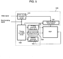
- Fig. 5 is a diagram showing an example of a circuit block of a driver for implementing the method of driving the panel used for the exemplary embodiment.
- Driver 100 of the exemplary embodiment of the present invention includes: video signal processor circuit 101, data electrode driver circuit 102, timing controller circuit 103, scan electrode driver circuit 104 and sustain electrode driver circuit 105, and priming electrode driver circuit 106.
- a video signal and synchronizing signal are fed into video signal processor circuit 101. Responsive to the video signal and synchronizing signal, video signal processor circuit 101 outputs a sub-field signal for controlling whether or not to light each sub-field, to data electrode driver circuit 102.
- the synchronizing signal is also fed into timing controller circuit 103. Responsive to the synchronizing signal, timing controller circuit 103 outputs a timing control signal to data electrode driver circuit 102, scan electrode driver circuit 104, sustain electrode driver circuit 105, and priming electrode driver circuit 106.
- data electrode driver circuit 102 applies a predetermined driving waveform to the data electrodes (data electrodes D 1 to D m in Fig. 3) in the panel.
- scan electrode driver circuit 104 applies a predetermined driving waveform to the scan electrodes (scan electrodes SC 1 to SC n in Fig. 3) in the panel.
- sustain electrode driver circuit 105 applies a predetermined driving waveform to the sustain electrodes (sustain electrodes SU 1 to SU n in Fig. 3) in the panel.
- priming electrode driver circuit 106 applies a predetermined driving waveform to the priming electrodes (priming electrodes PR 1 to PR n-1 in Fig. 3) in the panel. Necessary electric power is supplied to data electrode driver circuit 102, scan electrode driver circuit 104, sustain electrode driver circuit 105, and priming electrode driver circuit 106 from a power supply circuit (not shown).
- the above circuit block can constitute a driver for implementing the method of driving the panel of the exemplary embodiment.
- the present invention can provide a method of driving a plasma display panel capable of performing stable and high-speed writing operation.
- the method of driving a plasma display panel of the present invention can perform stable and high-speed writing operation.
- the present invention is useful as a method of driving a plasma display panel.
Abstract
Description
- The present invention relates to a method of driving a plasma display panel.
- A plasma display panel (hereinafter abbreviated as a PDP or a panel) is a display device having excellent visibility and featuring a large screen, thinness and light weight. The systems of discharging a PDP include an alternating-current (AC) type and direct-current (DC) type. The electrode structures thereof include a three-electrode surface-discharge type and an opposite-discharge type. However, the current mainstream is an AC type three-electrode PDP, which is an AC surface-discharge type, because this type of PDP is suitable for higher definition and easy to manufacture.
- Generally, an AC type three-electrode PDP has a large number of discharge cells formed between a front panel and rear panel faced with each other. In the front panel, a plurality of display electrodes, each made of a pair of scan electrode and sustain electrode, are formed on a front glass substrate in parallel with each other. A dielectric layer and a protective layer are formed to cover these display electrodes. In the rear panel, a plurality of parallel data electrodes is formed on a rear glass substrate. A dielectric layer is formed on the data electrodes to cover them. Further, a plurality of barrier ribs is formed on the dielectric layer in parallel with the data electrodes. Phosphor layers are formed on the surface of the dielectric layer and the side faces of the barrier ribs. Then, the front panel and the rear panel are faced with each other and sealed together so that the display electrodes and data electrodes intersect with each other. A discharge gas is filled into an inside discharge space formed therebetween. In a panel structured as above, ultraviolet light is generated by gas discharge in each discharge cell. This ultraviolet light excites respective phosphors to emit R, G, or B color, for color display.
- A general method of driving a panel is a so-called sub-field method: one field period is divided into a plurality of sub-fields and combination of light-emitting sub-fields provides gradation images for display. Now, each of the sub-fields has an initializing period, writing period, and sustaining period.
- In the initializing period, all the discharge cells perform initializing discharge operation at a time to erase the history of wall electric charge previously formed in respective discharge cells and form wall electric charge necessary for the subsequent writing operation. Additionally, this initializing discharge operation serves to generate priming (priming for discharge = excited particles) for causing stable writing discharge.
- In the writing period, scan pulses are sequentially applied to scan electrodes, and write pulses corresponding to the signals of an image to be displayed are applied to data electrodes. Thus, selective writing discharge is caused between scan electrodes and corresponding data electrodes for selective formation of wall electric charge.
- In the subsequent sustaining period, a predetermined number of sustain pulses are applied between scan electrodes and corresponding sustain electrodes. Then, the discharge cells in which wall electric charge are formed by the writing discharge are selectively discharged and light is emitted from the discharge cells.
- In this manner, to properly display an image, selective writing discharge must securely be performed in the writing period. However, there are many factors in increasing discharge delay in the writing discharge: restraints of the circuitry inhibit the use of high voltage for write pulses; and phosphor layers formed on the data electrodes make discharge difficult. For these reasons, priming for generating stable writing discharge is extremely important.
- However, the priming caused by discharge rapidly decreases as time elapses. This causes the following problems in the method of driving a panel described above. In writing discharge occurring long time after the initializing discharge, priming generated in the initializing discharge is insufficient. This insufficient priming causes a large discharge delay and unstable wiring operation, thus degrading the image display quality. Additionally, when long wiring period is set for stable wiring operation, the time taken for the writing period is too long.
- Proposed to address these problems are a panel and method of driving the panel in which auxiliary discharge electrodes are provided and discharge delay is minimized using priming caused by auxiliary discharge (see Japanese Patent Unexamined Publication No. 2002-297091, for example).
- However, such panels have the following problems. Because the discharge delay of the auxiliary discharge itself is large, the discharge delay of the writing discharge cannot sufficiently be shortened. Additionally, because the operating margin of the auxiliary discharge is small, incorrect discharge may be induced in some panels.
- Further, when the number of scan electrodes is increased for higher definition without shortening the discharge delay in the writing discharge sufficiently, the time taken for the writing period is too long and the time taken for the sustaining period is insufficient. As a result, luminance decreases. Additionally, increasing the partial pressure of xenon to increase the luminance and efficiency further increases the discharge delay and makes the writing operation unstable.
- The present invention addresses these problems and aims to provide a method of driving a plasma display panel capable of performing stable and high-speed writing operation.
- To address these problems, in the method of driving a plasma display panel of the present invention, the pulse width of scan pulses applied to scan electrodes in which writing operation is performed but no priming discharge is caused with the scanning of the scan electrodes is shorter than the pulse width of scan pulses applied to other scan electrodes in which writing operation is performed and priming discharge is caused with the scanning of the scan electrodes, in the writing period.
-
- Fig. 1 is a sectional view showing an example of a panel used for an exemplary embodiment of the present invention.
- Fig. 2 is a schematic perspective view showing a structure of a rear substrate side of the panel.
- Fig. 3 is a diagram showing an arrangement of electrodes in the panel.
- Fig. 4 is a diagram showing a driving waveform in a method of driving the panel.
- Fig. 5 is diagram showing an example of a circuit block of a driver for implementing the method of driving the panel.
-
- A method of driving a plasma display panel in accordance with an exemplary embodiment of the present invention is described hereinafter with reference to the accompanying drawings.
- Fig. 1 is a sectional view showing an example of a panel used for the exemplary embodiment of the present invention. Fig. 2 is a schematic perspective view showing the structure of the rear substrate side of the panel.
- As shown in Fig. 1,
front substrate 1 andrear substrate 2 both made of glass are faced with each other to sandwich a discharge space therebetween. In the discharge space, a mixed gas of neon and xenon for radiating ultraviolet light by discharge is filled. - On
front substrate 1, a plurality of pairs ofscan electrode 6 and sustainelectrode 7 are formed in parallel with each other. Further,scan electrodes 6 and sustainelectrodes 7 are alternately arranged in pairs like sustain electrode 7 - scan electrode 6 - scan electrode 6 - sustain electrode 7 - sustain electrode 7 -scan electrode 6, etc.Scan electrode 6 and sustainelectrode 7 are made oftransparent electrodes metal buses transparent electrodes scan electrode 6 and theother scan electrode 6, and one sustainelectrode 7 and theother scan electrode 7, light-absorbinglayers 8, each made of a black material, are provided.Projection 6b' ofmetal bus 6b in one ofadjacent scan electrodes 6 projects onto light-absorbinglayer 8.Dielectric layer 4 andprotective layer 5 are formed to cover thesescan electrodes 6, sustainelectrodes 7, and light-absorbinglayers 8. - On
rear substrate 2, a plurality ofdata electrodes 9 is formed in parallel with each other.Dielectric layer 15 is formed to cover thesedata electrodes 9. Further on the dielectric layer,barrier ribs 10 for partitioning the discharge space intodischarge cells 11 are formed. As shown in Fig. 2, eachbarrier rib 10 is made ofvertical walls 10a extending in parallel withdata electrodes 9, andhorizontal walls 10b for formingdischarge cells 11 and formingclearance 13 betweendischarge cells 11. Inclearance 13 faced withprojection 6b' inscan electrode 6 amongclearances 13, primingelectrode 14 is formed in the direction orthogonal todata electrodes 9, to form primingcell 13a. In other words, primingelectrodes 14 are not provided in all theclearances 13, and are formed in primingcells 13 in every other one ofclearances 13. On the surface ofdielectric layer 15 corresponding to dischargecells 11 and the side faces ofbarrier ribs 10, phosphor layers 12 are provided. However, nophosphor layer 12 is formed on the side ofclearances 13. - When
front substrate 1 is faced and sealed withrear substrate 2, eachprojection 6b' ofmetal bus 6b inscan electrode 6 formed onfront substrate 1 that projects onto light-absorbinglayer 8 is positioned in parallel withcorresponding priming electrode 14 onrear substrate 2 and faced therewith in primingcell 13a. In other words, the panel shown in Figs. 1 and 2 is structured to includepriming cells 13a, each for performing priming discharge betweenprojection 6b' formed on the side offront substrate 1 andpriming electrode 14 formed on the side ofrear substrate 2. - In Figs. 1 and 2,
dielectric layer 16 is further formed to coverpriming electrodes 14. - Now, to facilitate causing priming discharge, phosphor layers 12 that hinder the discharge are not provided on priming
cells 13a. Further, the interval betweenprojection 6b' inscan electrode 6 andcorresponding priming electrode 14 is shorter than the interval betweendata electrode 9 andcorresponding scan electrode 6. Thus, the discharge-starting voltage of the priming discharge is lower than that of the writing discharge, and the priming discharge is more likely to occur. - Fig. 3 is a diagram showing an arrangement of electrodes in the panel used for the exemplary embodiment of the present invention. M columns of data electrodes D1 to Dm (
data electrodes 9 in Fig. 1) are arranged in the column direction. N rows of scan electrodes SC1 to SCn (scanelectrodes 6 in Fig. 1), and n rows of sustain electrodes SU1 to SUn (sustainelectrodes 7 in Fig. 1) are alternately arranged in pairs in the row direction like sustain electrode SU1 - scan electrode SC1 - scan electrode SC2 - sustain electrode SU2, etc. In this embodiment,projections 6b' are provided only in odd-numbered scan electrodes SU1, SU3, etc. N/2 rows of priming electrodes PR1, PR3, etc. (primingelectrode 14 in Fig. 1) are arranged to be faced with the corresponding projections of these scan electrodes SU1, SU3, etc. - Thus, m x n discharge cells Cij (discharge
cells 11 in Fig. 1), each including a pair of scan electrode SCi and sustain electrode SUi (i = 1 to n) and one data electrode Dj (j = 1 to m), are formed in the discharge space. N/2 rows of priming cells Pp (primingcell 13a in Fig. 1), each includingprojection 6b' of scan electrode SCp (p = odd number) and priming electrode PRp, are formed. - As described above, the panel used in the embodiment of the present invention, odd-numbered scan electrodes SCp are scan electrodes with
projections 6b' in which writing operation is performed and priming discharge is caused with the scanning of the scan electrodes. On the other hand, even-numbered scan electrodes SCp+1 are scan electrodes with noprojections 6b in which writing operation is performed but no priming discharge is caused with the scanning of the scan electrodes. - Next, a driving waveform for driving the panel and timing of the driving waveform are described.
- Fig. 4 is a diagram showing a driving waveform in the method of driving the panel used for the exemplary embodiment of the present invention. In this embodiment, one field period is made of a plurality of sub-fields, each including an initializing period, writing period, and sustaining period. Because the same operation is performed in each sub-field, except for the number of sustain pulses in the sustaining period, operation in one sub-filed is described hereinafter.
- In the former half of the initializing period, each of data electrodes D1 to Dm, sustain electrode SU1 to SUn, and priming electrodes PR1 to PRn-1 is held at 0 (V). Applied to each of scan electrodes SC1 to SCn is a ramp waveform voltage gradually increasing from a voltage of Vi1 not larger than discharge-starting voltage across the scan electrodes and sustain electrodes SU1 to SUn to a voltage of Vi2 exceeding the discharge-starting voltage. While the ramp waveform voltage increases, first weak initializing discharge occurs between scan electrodes SC1 to SCn, and sustain electrodes SU1 to SUn, data electrodes D1 to Dm, and priming electrodes PR1 to PRn-1. Thus, negative wall voltage accumulates on scan electrodes SC1 to SCn, and positive wall voltage accumulates on data electrodes D1 to Dm, sustain electrodes SU1 to SUn, and priming electrodes PR1 to PRn-1. Now, the wall voltage on the electrodes is the voltage generated by the wall charge accumulating on the dielectric layers covering the electrodes.
- In the latter half of the initializing period, each of sustain electrode SU1 to SUn is held at a positive voltage of Ve. Applied to each of scan electrodes SC1 to SCn is a ramp waveform voltage gradually decreasing from a voltage of Vi3 not larger than discharge-starting voltage across the scan electrodes and sustain electrodes SU1 to SUn to a voltage of Vi4 exceeding the discharge-starting voltage. During this application of the ramp voltage, second weak initializing discharge occurs between scan electrodes SC1 to SCn, and sustain electrodes SU1 to SUn, data electrodes D1 to Dm, and priming electrodes PR1 to PRn-1. Then, the negative wall voltage on scan electrodes SC1 to SCn and the positive wall voltage on sustain electrodes SU1 to SUn are weakened. The positive wall voltage on data electrodes D1 to Dm is adjusted to a value appropriate for writing operation. The positive wall voltage on priming electrodes PR1 to PRn-1 is also adjusted to a value appropriate for priming operation. Thus, the initializing operation is completed.
- In the writing period, scan electrodes SC1 to SCn are once held at a voltage of Vc. Then, a voltage of Vq substantially equal to voltage change Vc - Vi4 is applied to priming electrodes PR1 to PRn-1.
- Next, scan pulse Va is applied to scan electrode SC1 of the first row. Then, priming discharge occurs between priming electrode PR1 and
projection 6b' in scan electrode SC1. The priming diffuses inside of discharge cells C1,1 to C1, m in the first row corresponding to scan electrode SC1 of the first row and discharge cells C2,1 to C2,m in the second row corresponding to scan electrode SC2 of the second row. Because the priming cells are structured to easily discharge as described above, in this discharge, high-speed and stable priming discharge with a small discharge delay is obtained. - At the same time, positive write pulse voltage Vd is applied to data electrode Dk (k being an integer ranging from 1 to m) corresponding to the signal of an image to be displayed in the first row, among data electrodes D1 to Dm. Then, discharge occurs at the intersection of data electrode Dk to which write pulse voltage Vd has been applied and scan electrode SC1. This discharge develops to the discharge between sustain electrode SU1 and scan electrode SC1 in corresponding discharge cell C1,k. Then, positive voltage accumulates on scan electrode SC1 and negative voltage accumulates on sustain electrode SU1 in discharge cell C1,k. Thus, the writing operation in the first row is completed. As described above, because the priming discharge and writing discharge sequentially occur in the scanning period in the first row, the pulse width of the scan pulse applied to scan electrode SC1 of the first row is the sum of time tp necessary for the priming discharge and time tw necessary for the writing operation, i.e. tp + tw.
- Now, scan electrode SC1 of the first row is a scan electrode in which writing is performed and the priming discharge is caused with scanning of the scan electrode. The discharge in discharge cell C1,k occurs with the priming supplied from the priming discharge that has occurred between scan electrode SC1 and priming electrode PR1. For this reason, although there is a delay in starting the supply of the priming from the priming cell, stable discharge with a small discharge delay can be obtained after the supply of the priming.
- Next, scan pulse voltage Va having a pulse width smaller than the pulse width of the pulse applied to the scan electrode of the first row is applied to scan electrode SC2 of the second row. At this time, positive write pulse voltage Vd is applied to data electrode Dk corresponding to the signal of the image to be displayed in the second row, among data electrodes D1 to Dm. Then, discharge occurs at the intersection of data electrode Dk and scan electrode SC2. This discharge develops to the discharge between sustain electrode SU2 and scan electrode SC2 in corresponding discharge cell C2,k. Then, positive voltage accumulates on scan electrode SC2 and negative voltage accumulates on sustain electrode SU2 in discharge cell C2,k. Thus, the writing operation in the second row is completed.
- Now, the reason why the pulse width of the scan pulse applied to scan electrode SC2 of the second row is smaller than the first pulse width, i.e. tp + tw, is as follows. Scan electrode SC2 is a scan electrode in which writing is performed but no priming discharge is caused with the scanning of the scan electrode. Thus, the discharge in discharge cell C2,k occurs with sufficient priming already supplied from the priming discharge that has occurred between scan electrode SC1 and priming electrode PR1. Therefore, time tp necessary for the priming discharge need not take into account. At this time, of course, the discharge delay in the writing discharge is extremely small and stable discharge can be obtained.
- In a similar manner, a scan pulse having the first pulse width of tp + tw is applied to scan electrode SC3 of the third row, and a write pulse is applied to data electrode Dk. Then, priming discharge occurs between priming electrode PR3 and scan electrode SC3 first, and priming is supplied to discharge cells C3,1 to C3,m in the third row and discharge cells C4,1 to C4,m in the fourth row. Successively, writing discharge occurs in discharge cell C3,k corresponding to data electrode Dk to which the write pulse voltage has been applied.
- Next, a scan pulse having a pulse width of tw is applied to scan electrode SC4 of the fourth row, and a positive write pulse is applied to data electrode Dk. Then, in corresponding discharge cell C3,k, stable writing discharge with an extremely a small discharge delay is caused by the influence of the priming already supplied.
- The similar writing operations are performed in discharge cells including Cn,k of the n-th row, and the writing operations are completed.
- In this manner, in the writing operation in each of discharge cells Cp,1 to Cp,m (p = odd number) in an odd-numbered row, a scan pulse having the first pulse width of tp + tw is applied to scan electrode SCp, and a write pulse is applied to data electrode Dk. Then, priming discharge occurs between priming electrodes PRp and scan electrodes SCp first, and the priming is supplied inside of discharge cells Cp,1 to Cp,m and discharge cells Cp+1,1 to Cp+1,m. Successively, writing discharge occurs in discharge cell Cp,k corresponding to data electrode Dk to which the write pulse voltage has been applied.
- Next, in the writing operation in each of discharge cells Cp+1,1 to Cp+1,m in even-numbered row, a scan pulse having a pulse width of tw is applied to scan electrode SCp+1 of the (p+1)-th row, and a write pulse is applied to data electrode Dk. Then, in corresponding discharge cell Cp+1, k, stable writing discharge having an extremely a small discharge delay is caused by the influence of the priming already supplied.
- In the sustaining period, after scan electrodes SC1 to SCn and sustain electrodes SU1 to SUn are reset to 0 (V) once, a positive sustain pulse voltage of Vs is applied to scan electrodes SC1 to SCn. At this time, in the voltage on scan electrode SCi and sustain electrode SUi in discharge cell Ci,j in which writing discharge has occurred, the wall voltage accumulating on scan electrode SCi and sustain electrode SUi is added to sustain pulse voltage Vs. For this reason, the voltage exceeds the discharge-starting voltage and sustain discharge occurs. In a similar manner, by alternately applying sustain pulses to scan electrodes SC1 to SCn and sustain electrodes SU1 to SUn, sustain discharge operations are successively performed in discharge cell Ci,k in which the writing discharge has occurred, the number of times of sustain pulses.
- As described above, unlike the writing discharge depending only on the priming in the initializing discharge in accordance with a conventional driving method, the writing discharge of the method of driving a panel in accordance with this embodiment of the present invention is performed with sufficient priming supplied from the priming discharge that has occurred during or immediately before the writing operation in respective discharge cells. This can achieve high-speed and stable writing discharge with a small discharge delay, and display a high-quality image.
- Further, electrodes in the vicinity of the priming cells are priming
electrodes 14 andscan electrodes 6 only. This also gives an advantage of stable action of the priming discharge itself because the priming discharge is unlikely to cause other unnecessary discharge, e.g. incorrect discharge involving the sustain electrodes. - Incidentally, because respective electrodes of an AC type PDP are surrounded by the dielectric layers and insulated from the discharge space. For this reason, direct-current components make no contribution to discharge itself. Therefore, of course, even the use of a waveform in which direct-current components are added to the driving waveform of the exemplary embodiment of the present invention can provide similar effects.
- Fig. 5 is a diagram showing an example of a circuit block of a driver for implementing the method of driving the panel used for the exemplary embodiment.
Driver 100 of the exemplary embodiment of the present invention includes: videosignal processor circuit 101, dataelectrode driver circuit 102,timing controller circuit 103, scanelectrode driver circuit 104 and sustainelectrode driver circuit 105, and primingelectrode driver circuit 106. A video signal and synchronizing signal are fed into videosignal processor circuit 101. Responsive to the video signal and synchronizing signal, videosignal processor circuit 101 outputs a sub-field signal for controlling whether or not to light each sub-field, to dataelectrode driver circuit 102. The synchronizing signal is also fed intotiming controller circuit 103. Responsive to the synchronizing signal,timing controller circuit 103 outputs a timing control signal to dataelectrode driver circuit 102, scanelectrode driver circuit 104, sustainelectrode driver circuit 105, and primingelectrode driver circuit 106. - Responsive to the sub-field signal and the timing control signal, data
electrode driver circuit 102 applies a predetermined driving waveform to the data electrodes (data electrodes D1 to Dm in Fig. 3) in the panel. Responsive to the timing control signal, scanelectrode driver circuit 104 applies a predetermined driving waveform to the scan electrodes (scan electrodes SC1 to SCn in Fig. 3) in the panel. Responsive to the timing control signal, sustainelectrode driver circuit 105 applies a predetermined driving waveform to the sustain electrodes (sustain electrodes SU1 to SUn in Fig. 3) in the panel. Responsive to the timing control signal, primingelectrode driver circuit 106 applies a predetermined driving waveform to the priming electrodes (priming electrodes PR1 to PRn-1 in Fig. 3) in the panel. Necessary electric power is supplied to dataelectrode driver circuit 102, scanelectrode driver circuit 104, sustainelectrode driver circuit 105, and primingelectrode driver circuit 106 from a power supply circuit (not shown). - The above circuit block can constitute a driver for implementing the method of driving the panel of the exemplary embodiment.
- As described above, the present invention can provide a method of driving a plasma display panel capable of performing stable and high-speed writing operation.
- As described above, the method of driving a plasma display panel of the present invention can perform stable and high-speed writing operation. Thus, the present invention is useful as a method of driving a plasma display panel.
Claims (1)
- A method of driving a plasma display panel comprising a plurality of scan electrodes and sustain electrodes arranged in parallel with each other, and a plurality of data electrodes arranged in a direction intersecting the scan electrodes, in which one field period is made of a plurality of sub-fields, each including an initializing period, writing period, and sustaining period, the method comprising:providing a plurality of priming electrodes in parallel with the scan electrodes, the priming electrodes generating priming discharge between the priming electrodes and the corresponding scan electrodes; andin the writing period, making a pulse width of a scan pulse applied to some of the scan electrodes in which writing is performed but no priming discharge is caused with scanning of the scan electrodes smaller than a pulse width of a scan pulse applied to the other scan electrodes in which writing is performed and priming discharge is caused with scanning of the scan electrodes.
Applications Claiming Priority (3)
| Application Number | Priority Date | Filing Date | Title |
|---|---|---|---|
| JP2003080302A JP3888321B2 (en) | 2003-03-24 | 2003-03-24 | Driving method of plasma display panel |
| JP2003080302 | 2003-03-24 | ||
| PCT/JP2004/003946 WO2004086340A1 (en) | 2003-03-24 | 2004-03-23 | Drive method for plasma display panel |
Publications (2)
| Publication Number | Publication Date |
|---|---|
| EP1607930A1 true EP1607930A1 (en) | 2005-12-21 |
| EP1607930A4 EP1607930A4 (en) | 2009-03-18 |
Family
ID=33094868
Family Applications (1)
| Application Number | Title | Priority Date | Filing Date |
|---|---|---|---|
| EP04722693A Withdrawn EP1607930A4 (en) | 2003-03-24 | 2004-03-23 | Drive method for plasma display panel |
Country Status (6)
| Country | Link |
|---|---|
| US (1) | US7298349B2 (en) |
| EP (1) | EP1607930A4 (en) |
| JP (1) | JP3888321B2 (en) |
| KR (1) | KR100661683B1 (en) |
| CN (1) | CN100390843C (en) |
| WO (1) | WO2004086340A1 (en) |
Cited By (1)
| Publication number | Priority date | Publication date | Assignee | Title |
|---|---|---|---|---|
| WO2004114271A1 (en) | 2003-06-24 | 2004-12-29 | Matsushita Electric Industrial Co., Ltd. | Plasma display apparatus and method for driving the same |
Families Citing this family (5)
| Publication number | Priority date | Publication date | Assignee | Title |
|---|---|---|---|---|
| KR100705836B1 (en) * | 2004-11-10 | 2007-04-10 | 엘지전자 주식회사 | Method for Driving Plasma Display Panel |
| KR100793094B1 (en) * | 2005-09-23 | 2008-01-10 | 엘지전자 주식회사 | Plasma Display Apparatus and Driving Method therof |
| KR100814830B1 (en) | 2006-11-22 | 2008-03-20 | 삼성에스디아이 주식회사 | Plasma display device and driving method thereof |
| WO2011089886A1 (en) * | 2010-01-19 | 2011-07-28 | パナソニック株式会社 | Plasma display panel driving method and plasma display device |
| WO2011089887A1 (en) * | 2010-01-19 | 2011-07-28 | パナソニック株式会社 | Plasma display panel driving method and plasma display device |
Citations (1)
| Publication number | Priority date | Publication date | Assignee | Title |
|---|---|---|---|---|
| US6313580B1 (en) * | 1998-04-14 | 2001-11-06 | Nec Corporation | AC-discharge type plasma display panel and method for driving the same |
Family Cites Families (12)
| Publication number | Priority date | Publication date | Assignee | Title |
|---|---|---|---|---|
| JP2581465B2 (en) * | 1994-09-28 | 1997-02-12 | 日本電気株式会社 | Plasma display panel and driving method thereof |
| JP3231569B2 (en) * | 1995-02-13 | 2001-11-26 | 日本電気株式会社 | Driving method and driving apparatus for plasma display panel |
| JPH09245627A (en) * | 1996-03-07 | 1997-09-19 | Mitsubishi Electric Corp | Gas discharge display device, manufacture thereof and drive method of panel thereof |
| JP3517551B2 (en) * | 1997-04-16 | 2004-04-12 | パイオニア株式会社 | Driving method of surface discharge type plasma display panel |
| US6043605A (en) * | 1997-07-04 | 2000-03-28 | Samsung Display Devices Co., Ltd. | Plasma display device with auxiliary electrodes and protective layer |
| KR100300407B1 (en) * | 1998-10-14 | 2001-09-06 | 김순택 | Plasma display device |
| KR100364696B1 (en) * | 1999-10-28 | 2003-01-24 | 엘지전자 주식회사 | Method for driving plasma display panel and structure of the plasma display panel |
| JP3512075B2 (en) * | 2000-03-23 | 2004-03-29 | 日本電気株式会社 | Driving method of plasma display panel |
| TW518539B (en) * | 2000-08-28 | 2003-01-21 | Matsushita Electric Ind Co Ltd | Plasma display panel with superior luminous characteristics |
| JP2002351397A (en) * | 2001-05-24 | 2002-12-06 | Nec Corp | Driving device for plasma display device |
| TWI226596B (en) * | 2001-07-09 | 2005-01-11 | Matsushita Electric Ind Co Ltd | Driving method for plasma display panel and driving apparatus for plasma display panel |
| TW525201B (en) * | 2001-12-07 | 2003-03-21 | Au Optronics Corp | Plasma display panel having priming electrode and the driving electrode thereof |
-
2003
- 2003-03-24 JP JP2003080302A patent/JP3888321B2/en not_active Expired - Fee Related
-
2004
- 2004-03-23 EP EP04722693A patent/EP1607930A4/en not_active Withdrawn
- 2004-03-23 WO PCT/JP2004/003946 patent/WO2004086340A1/en active Application Filing
- 2004-03-23 US US10/515,503 patent/US7298349B2/en not_active Expired - Fee Related
- 2004-03-23 CN CNB2004800005048A patent/CN100390843C/en not_active Expired - Fee Related
- 2004-03-23 KR KR1020057001027A patent/KR100661683B1/en not_active IP Right Cessation
Patent Citations (1)
| Publication number | Priority date | Publication date | Assignee | Title |
|---|---|---|---|---|
| US6313580B1 (en) * | 1998-04-14 | 2001-11-06 | Nec Corporation | AC-discharge type plasma display panel and method for driving the same |
Non-Patent Citations (1)
| Title |
|---|
| See also references of WO2004086340A1 * |
Cited By (4)
| Publication number | Priority date | Publication date | Assignee | Title |
|---|---|---|---|---|
| WO2004114271A1 (en) | 2003-06-24 | 2004-12-29 | Matsushita Electric Industrial Co., Ltd. | Plasma display apparatus and method for driving the same |
| EP1640945A1 (en) * | 2003-06-24 | 2006-03-29 | Matsushita Electric Industrial Co., Ltd. | Plasma display apparatus and driving method thereof |
| EP1640945A4 (en) * | 2003-06-24 | 2008-09-24 | Matsushita Electric Ind Co Ltd | Plasma display apparatus and driving method thereof |
| US7477209B2 (en) | 2003-06-24 | 2009-01-13 | Panasonic Corporation | Plasma display apparatus and driving method thereof |
Also Published As
| Publication number | Publication date |
|---|---|
| JP2004287175A (en) | 2004-10-14 |
| JP3888321B2 (en) | 2007-02-28 |
| CN100390843C (en) | 2008-05-28 |
| WO2004086340A1 (en) | 2004-10-07 |
| KR100661683B1 (en) | 2006-12-26 |
| US20050200570A1 (en) | 2005-09-15 |
| CN1698081A (en) | 2005-11-16 |
| US7298349B2 (en) | 2007-11-20 |
| KR20050021524A (en) | 2005-03-07 |
| EP1607930A4 (en) | 2009-03-18 |
Similar Documents
| Publication | Publication Date | Title |
|---|---|---|
| KR100341313B1 (en) | Plasma Display Panel And Apparatus And Method Of Driving The Same | |
| US7345655B2 (en) | Plasma display panel drive method | |
| US7342558B2 (en) | Plasma display panel drive method | |
| US7298349B2 (en) | Drive method for plasma display panel | |
| US20060164338A1 (en) | Plasma display panel drive method | |
| US7330165B2 (en) | Method of driving plasma display panel | |
| JP4325237B2 (en) | Plasma display panel | |
| JP4075878B2 (en) | Driving method of plasma display panel | |
| JP4569136B2 (en) | Driving method of plasma display panel | |
| JP4239779B2 (en) | Plasma display panel | |
| JP4461733B2 (en) | Driving method of plasma display panel | |
| JP2006351259A (en) | Plasma display panel | |
| JP2007133291A (en) | Driving method of plasma display panel | |
| JP4547949B2 (en) | Driving method of plasma display panel | |
| JP4507709B2 (en) | Driving method of plasma display panel | |
| JP2005338458A (en) | Method for driving plasma display panel, and plasma display apparatus | |
| JP2005037821A (en) | Driving method of plasma display panel | |
| JP2006172800A (en) | Plasma display panel and its driving method | |
| JP2007133207A (en) | Method for driving plasma display panel and plasma display device |
Legal Events
| Date | Code | Title | Description |
|---|---|---|---|
| PUAI | Public reference made under article 153(3) epc to a published international application that has entered the european phase |
Free format text: ORIGINAL CODE: 0009012 |
|
| 17P | Request for examination filed |
Effective date: 20041124 |
|
| AK | Designated contracting states |
Kind code of ref document: A1 Designated state(s): AT BE BG CH CY CZ DE DK EE ES FI FR GB GR HU IE IT LI LU MC NL PL PT RO SE SI SK TR |
|
| AX | Request for extension of the european patent |
Extension state: AL LT LV MK |
|
| DAX | Request for extension of the european patent (deleted) | ||
| RBV | Designated contracting states (corrected) |
Designated state(s): DE FR GB NL |
|
| RAP1 | Party data changed (applicant data changed or rights of an application transferred) |
Owner name: PANASONIC CORPORATION |
|
| A4 | Supplementary search report drawn up and despatched |
Effective date: 20090217 |
|
| 17Q | First examination report despatched |
Effective date: 20091210 |
|
| GRAP | Despatch of communication of intention to grant a patent |
Free format text: ORIGINAL CODE: EPIDOSNIGR1 |
|
| RIC1 | Information provided on ipc code assigned before grant |
Ipc: G09G 3/288 20060101AFI20120214BHEP |
|
| RIN1 | Information on inventor provided before grant (corrected) |
Inventor name: OGAWA, KENJI Inventor name: NAGAO, NOBUAKI Inventor name: KIGO, SHIGEO Inventor name: WAKABAYASHI, TOSHIKAZU Inventor name: TACHIBANA, HIROYUKI |
|
| STAA | Information on the status of an ep patent application or granted ep patent |
Free format text: STATUS: THE APPLICATION IS DEEMED TO BE WITHDRAWN |
|
| 18D | Application deemed to be withdrawn |
Effective date: 20120731 |