EP1607719A2 - Magnetic sensor - Google Patents
Magnetic sensor Download PDFInfo
- Publication number
- EP1607719A2 EP1607719A2 EP05445037A EP05445037A EP1607719A2 EP 1607719 A2 EP1607719 A2 EP 1607719A2 EP 05445037 A EP05445037 A EP 05445037A EP 05445037 A EP05445037 A EP 05445037A EP 1607719 A2 EP1607719 A2 EP 1607719A2
- Authority
- EP
- European Patent Office
- Prior art keywords
- magnetic
- resistors
- heat treatment
- trimming
- magnetic sensor
- Prior art date
- Legal status (The legal status is an assumption and is not a legal conclusion. Google has not performed a legal analysis and makes no representation as to the accuracy of the status listed.)
- Withdrawn
Links
Images



Classifications
-
- G—PHYSICS
- G01—MEASURING; TESTING
- G01D—MEASURING NOT SPECIALLY ADAPTED FOR A SPECIFIC VARIABLE; ARRANGEMENTS FOR MEASURING TWO OR MORE VARIABLES NOT COVERED IN A SINGLE OTHER SUBCLASS; TARIFF METERING APPARATUS; MEASURING OR TESTING NOT OTHERWISE PROVIDED FOR
- G01D5/00—Mechanical means for transferring the output of a sensing member; Means for converting the output of a sensing member to another variable where the form or nature of the sensing member does not constrain the means for converting; Transducers not specially adapted for a specific variable
- G01D5/12—Mechanical means for transferring the output of a sensing member; Means for converting the output of a sensing member to another variable where the form or nature of the sensing member does not constrain the means for converting; Transducers not specially adapted for a specific variable using electric or magnetic means
- G01D5/14—Mechanical means for transferring the output of a sensing member; Means for converting the output of a sensing member to another variable where the form or nature of the sensing member does not constrain the means for converting; Transducers not specially adapted for a specific variable using electric or magnetic means influencing the magnitude of a current or voltage
- G01D5/142—Mechanical means for transferring the output of a sensing member; Means for converting the output of a sensing member to another variable where the form or nature of the sensing member does not constrain the means for converting; Transducers not specially adapted for a specific variable using electric or magnetic means influencing the magnitude of a current or voltage using Hall-effect devices
- G01D5/145—Mechanical means for transferring the output of a sensing member; Means for converting the output of a sensing member to another variable where the form or nature of the sensing member does not constrain the means for converting; Transducers not specially adapted for a specific variable using electric or magnetic means influencing the magnitude of a current or voltage using Hall-effect devices influenced by the relative movement between the Hall device and magnetic fields
-
- B—PERFORMING OPERATIONS; TRANSPORTING
- B82—NANOTECHNOLOGY
- B82Y—SPECIFIC USES OR APPLICATIONS OF NANOSTRUCTURES; MEASUREMENT OR ANALYSIS OF NANOSTRUCTURES; MANUFACTURE OR TREATMENT OF NANOSTRUCTURES
- B82Y25/00—Nanomagnetism, e.g. magnetoimpedance, anisotropic magnetoresistance, giant magnetoresistance or tunneling magnetoresistance
-
- G—PHYSICS
- G01—MEASURING; TESTING
- G01D—MEASURING NOT SPECIALLY ADAPTED FOR A SPECIFIC VARIABLE; ARRANGEMENTS FOR MEASURING TWO OR MORE VARIABLES NOT COVERED IN A SINGLE OTHER SUBCLASS; TARIFF METERING APPARATUS; MEASURING OR TESTING NOT OTHERWISE PROVIDED FOR
- G01D3/00—Indicating or recording apparatus with provision for the special purposes referred to in the subgroups
- G01D3/02—Indicating or recording apparatus with provision for the special purposes referred to in the subgroups with provision for altering or correcting the law of variation
- G01D3/021—Indicating or recording apparatus with provision for the special purposes referred to in the subgroups with provision for altering or correcting the law of variation using purely analogue techniques
-
- G—PHYSICS
- G01—MEASURING; TESTING
- G01R—MEASURING ELECTRIC VARIABLES; MEASURING MAGNETIC VARIABLES
- G01R33/00—Arrangements or instruments for measuring magnetic variables
- G01R33/02—Measuring direction or magnitude of magnetic fields or magnetic flux
- G01R33/06—Measuring direction or magnitude of magnetic fields or magnetic flux using galvano-magnetic devices
- G01R33/09—Magnetoresistive devices
- G01R33/093—Magnetoresistive devices using multilayer structures, e.g. giant magnetoresistance sensors
Definitions
- the present invention relates to a magnetic sensor for detecting the steering angle of a steering wheel.
- a prior art magnetic sensor 101 includes four magnetic resistors 111 to 114, which configure a Wheatstone bridge.
- the voltage difference of a node Q1, between the magnetic resistors 111 and 112, and a node Q2, between the magnetic resistors 113 and 114 is close to zero volts.
- the voltage difference is an offset voltage, which is the difference between median potentials E1 and E2 of the bridge.
- Fig. 2 is an enlarged diagram showing the four magnetic resistors 111 to 114.
- Each of the magnetic resistors 111 to 114 is a thin film having a certain pattern and is formed on a substrate 110 of the magnetic sensor 101.
- the magnetic resistor 111 includes a magnetic detection portion 121, a rough adjustment portion 131, and a fine adjustment portion 141.
- the magnetic detection portion 121 is extremely narrow.
- the rough adjustment portion 131 is narrow and ladder-like.
- the fine adjustment portion 141 is extremely wide.
- the other magnetic resistors 112, 113, and 114 each have the same configuration as the magnetic resistor 111 and respectively include magnetic detection portions 122, 123, and 124, rough adjustment portions 132, 133, and 134, and fine adjustment portions 142, 143, and 144.
- the patterns of the magnetic resistors 111 to 114 are determined so as to equalize the electric resistances R11 to R14.
- the offset voltage E12 is close to zero volts, and equation (1) is satisfied.
- the electric resistances R11 to R14 tend to differ from each other. Factors causing such differences include the formation accuracy of thin films and the etching accuracy for patterning the magnetic resistors 111 to 114. However, even if the thin film formation accuracy and etching accuracy for patterning the magnetic resistors 111 to 114 were to be improved, it would still be difficult to satisfy equation (1).
- Japanese Laid-Open Patent Publication No. 05-034224 proposes laser trimming in which the magnetic resistors 111 to 114 are partially cut with a laser beam to finely adjust the electric resistances R11 to R14.
- the laser trimming partially cuts one of the four magnetic resistors 111 to 114. This increases the resistance of the partially cut magnetic resistor and satisfies equation (1).
- Laser trimming is performed to cut part of the rough adjustment portion 132 (trimming section 132b) and part of the fine adjustment portion 142 (trimming section 142b).
- the magnetic resistor 112 receives the heat generated by irradiation of the laser beam.
- the magnetic resistors 111, 113, and 114 do not receive the heat of the laser beam irradiation.
- Change in the electric resistances R11 and R14 subsequent to laser trimming differs between the magnetic resistor 112, which is irradiated with a laser beam, and the magnetic resistors 111, 113, and 114, which are not irradiated with a laser beam.
- the electric resistance R12 of the magnetic resistor 112 changes at a rate that differs from the rate at which the electric resistances R11, R13, and R14 of the magnetic resistors 111, 113, and 114 change as time elapses.
- the equilibrium of the Wheatstone bridge (equation 1) cannot be maintained as time elapses.
- the offset voltage E12 changes from zero volts, immediately after the laser trimming, to a level that cannot be ignored in regard with the capacity of the magnetic sensor 101 (refer to Fig. 3).
- the magnetic sensor includes a plurality of magnetic resistors, each having an electric resistance that changes in accordance with change in magnetism.
- a plurality of heat treatment sections are fused by heat and respectively arranged in association with the magnetic resistors.
- Another aspect of the present invention is a method for manufacturing a magnetic sensor that detects change in magnetism.
- the method includes preparing a substrate, forming a plurality of magnetic resistors, each having a predetermined pattern, on the substrate, and trimming at least a selected one of the magnetic resistors to adjust the electric resistances of the magnetic resistors.
- the method further includes performing pre-trimming heat treatment to form a plurality of fused points prior to said trimming so that each magnetic resistor has at least one of the fused points.
- a magnetic sensor 1 according to a preferred embodiment of the present invention will now be described.
- the difference between the magnetic sensor 1 of the preferred embodiment and the magnetic sensor 101 of the prior art is that in addition to the section that is trimmed and cut to have the offset voltage approach 0 volts, there is a section that is heated and cut prior to trimming.
- the magnetic sensor 1 may be used as an angle sensor for detecting the steering angle of an automobile steering wheel.
- the magnetic sensor 1 includes four magnetic resistors 11 to 14, which configure a Wheatstone bridge.
- the magnetic resistors 11 to 14 are trimmed so that the difference between potential V1 at node P1 and potential V2 at node P2 (offset voltage V12) is substantially zero volts when the magnetic sensor 1 is arranged in a magnetic field of a predetermined direction. That is, when the electric resistances of the magnetic resistors 11, 12, 13, and 14 are respectively represented by R1, R2, R3, and R4, the magnetic resistors 11, 12, 13, and 14 are partially trimmed to satisfy equation (2).
- R1 ⁇ R4 R2 ⁇ R3
- the magnetic resistors 11 to 14 are thin films having a predetermined pattern and are formed on a substrate 10 of the magnetic sensor 1.
- the substrate 10 may be made of glass.
- the magnetic resistors 11 to 14 may each be made of a nickel-cobalt alloy.
- a nickel-cobalt alloy is a ferromagnetic material having a negative magnetic characteristic in which the electric resistance decreases as changes in the direction of the magnetic field increases.
- the magnetic resistors 11 to 14 form two groups. Each group includes two electrically opposed magnetic resistors. More specifically, the first group is formed by the magnetic resistors 11 and 14. The second group is formed by the magnetic resistors 12 and 13. The structure (arrangement) of the first group is symmetric (axisymmetric) to that of the second group with respect to a hypothetical line m.
- the magnetic resistor 11 includes a magnetic detection portion 21, a rough adjustment portion 31, and a fine adjustment portion 41.
- the electric resistance of the magnetic detection portion 21 changes (increases or decreases) in accordance with the level of change in the direction of the magnetic field.
- the magnetic detection portion 21 is extremely narrow.
- the rough adjustment portion 31 is narrow and ladder-like.
- the fine adjustment portion 41 is extremely wide.
- the rough adjustment portion 31 is partially trimmed and cut to greatly change the electric resistance R1 of the magnetic resistor 11. In other words, the rough adjustment portion 31 is trimmed to roughly increase the electric resistance R1 of the magnetic resistor 11.
- the fine adjustment portion 41 is partially trimmed and cut to finely change the electric resistance R1 of the magnetic resistor 11. In other words, the fine adjustment portion 41 is trimmed to finely increase the electric resistance R1 of the magnetic resistor 11.
- the magnetic resistors 12, 13, and 14 each have the same configuration as the magnetic resistor 111. Further, the magnetic resistors 12, 13, and 14 respectively include magnetic detection portions 22, 23, and 24, rough adjustment portions 32, 33, and 34, and fine adjustment portions 42, 43, and 44.
- the magnetic sensor 1 includes heat treatment sections (fused points) that undergo heat treatment prior to trimming. Every one of the magnetic resistors 11 to 14 includes at least one heat treatment section. In one embodiment, every one of the magnetic resistors 11 to 14 includes two heat treatment sections.
- the rough adjustment portion 31 of the magnetic resistor 11 includes a heat treatment section 31a that is thermally fused.
- the rough adjustment portions 32, 33, and 34 of the remaining magnetic resistors 12, 13, and 14 respectively include heat treatment sections 32a, 33a, and 34a. That is, each of the rough adjustment portions 31 to 34 in the magnetic sensor 1 includes at least one heat treatment section 31a, 32a, 33a, and 34a, respectively.
- the fine adjustment portion 41 of the magnetic resistor 11 includes a thermally fused heat treatment section 41a.
- the fine adjustment portions 42, 43, and 44 of the remaining magnetic resistors 12, 13, and 14 respectively include heat treatment sections 42a, 43a, and 44a. That is, each of the fine adjustment portions 41 to 44 in the magnetic sensor 1 includes at least one heat treatment section 41a, 42a, 43a, and 44a, respectively.
- the patterns of the magnetic resistors 11 to 14 are each determined so that the electric resistances R1 to R4 are equalized in a manner that the offset voltage V12 of the magnetic sensor 1 approaches zero volts (satisfies equation (2)) without performing trimming.
- the surface of the substrate 10 is sputtered in accordance with the pattern to form the films of the magnetic resistors 11 to 14.
- Film formation and photolithography are repeated to pattern the magnetic resistors 11 to 14. Then, a pre-trimming heat treatment is conducted on all of the magnetic resistors 11 to 14.
- the magnetic resistors 11 to 14 are each irradiated with a laser beam to form the heat treatment sections 31a to 34a and 41a to 44a.
- each of the rough adjustment portions 31 to 34 and each of the fine adjustment portions 41 to 44 are irradiated with a laser beam. This forms the heat treatment sections 31a to 34a and 41a to 44a, which have been fused by the heat of the laser beam.
- trimming is performed if necessary.
- selected ones of the magnetic resistors 11 to 14 are partially irradiated with a laser beam to cut part of the selected magnetic resistors 11 to 14. This cutting finely adjusts the electric resistances R1 to R4.
- each of the magnetic resistors 11 to 14 included in the magnetic sensor 1 receives heat.
- the heat affects the electric resistances R1 to R4 in the same manner in all of the magnetic resistors 11 to 14.
- the magnetic resistors 11 to 14 After the heat treatment sections 31a to 34a and 41a to 44a are formed in the magnetic resistors 11 to 14, trimming is performed on a selected one of the magnetic resistors (e.g., magnetic resistor 12). In this case, due to the heat generated by the trimming, it may be considered that the electric resistance R2 of the magnetic resistor 12 would change differently from the electric resistances of the other magnetic resistors and thereby cause the offset voltage V12 to change. However, the magnetic resistors 11 to 14 have all received heat prior to trimming during formation of the heat treatment sections 31a to 34a and 41a to 44a. Thus, at this point, the electric resistances R1 to R4 of the magnetic resistors 11 to 14 are thermally stabilized regardless of the application of the trimming heat.
- the electric resistances R1 to R4 of the magnetic resistors 11 to 14 are thermally stabilized regardless of the application of the trimming heat.
- the preferred embodiment has the advantages described below.
- the heat treatment sections do not have to be formed in the magnetic resistors 11 to 14 and may be formed at a location separated from the magnetic resistors 11 to 14. That is, the heat treatment sections may be independent from the magnetic resistors 11 to 14 or may be electrically disconnected from the magnetic resistors. This would also prevent the offset voltage V12 from changing as time elapses. In this case, since the magnetic resistors 11 to 14 are independent from the heat treatment sections, the heat generated during the pre-trimming heat treatment would be indirectly transmitted from the heat treatment sections to the magnetic resistors 11 to 14. This would prevent the electric resistances R1 to R4 of the magnetic resistors 11 to 14 from being significantly increased by the heat generated during the pre-trimming heat treatment.
- the heat treatment sections be located near the magnetic resistors 11 to 14 to apply the heat required to stabilize the electric resistances R1 to R4 within a short period of time.
- the heat treatment sections may be dummy portions separated from the magnetic resistors 11 to 14 and formed from the same material as the magnetic resistors 11 to 14.
- the dummy portions are formed during the film formation process. During the pre-trimming heat treatment, heat is applied to the dummy sections to fuse the dummy sections.
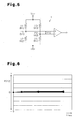
- Fig. 7 is a graph showing chronological changes in the offset voltage V12 of a magnetic sensor that includes fine adjustment portions 41 to 44, without the heat treatment sections 41a to 44a, and rough adjustment portions 31 to 34, with the heat treatment sections 31a to 34a. Chronological change in the offset voltage V12 is relatively small.
- the heat treatment section not be arranged in the magnetic detection portions 21 to 24, which detect changes in the direction of the magnetic field.
- heat be locally applied during the pre-trimming heat treatment that forms the heat treatment sections 31a to 34a and 41a to 44a.
- heat be applied in a short period of time (e.g., 0.5 seconds, which is less than one second) during the pre-trimming heat treatment that forms the heat treatment sections 31a to 34a and 41a to 44a.
- heat be applied at a high temperature (e.g., 1,500 degrees centigrade, which is greater than 1,000 degrees centigrade) during the pre-trimming heat treatment that forms the heat treatment sections 31a to 34a and 41a to 44a.
- a high temperature e.g., 1,500 degrees centigrade, which is greater than 1,000 degrees centigrade
- the magnetic resistors 11 to 14 may be made from a ferromagnetic material having a negative magnetic characteristic such as Permalloy.
- the material forming the magnetic resistors 11 to 14 is not limited to a ferromagnetic material having a negative magnetic characteristic. That is, the material forming the magnetic resistors 11 to 14 may be a semiconductor having a positive magnetic characteristic in which the electric resistance increases as the change in the direction of the magnetic field increases. Semiconductors having such positive magnetic characteristic include indium antimonide (InSb) alloys and gallium arsenide (GaAr) alloys.
Landscapes
- Physics & Mathematics (AREA)
- Engineering & Computer Science (AREA)
- General Physics & Mathematics (AREA)
- Chemical & Material Sciences (AREA)
- Nanotechnology (AREA)
- Technology Law (AREA)
- Condensed Matter Physics & Semiconductors (AREA)
- Crystallography & Structural Chemistry (AREA)
- Measuring Magnetic Variables (AREA)
- Hall/Mr Elements (AREA)
Abstract
Description
Claims (11)
- A magnetic sensor for detecting change in magnetism, the magnetic sensor including a plurality of magnetic resistors, each having an electric resistance that changes in accordance with change in magnetism, the magnetic sensor characterized by:a plurality of heat treatment sections fused by heat and respectively arranged in association with the magnetic resistors.
- The magnetic sensor according to claim 1, wherein each of the magnetic resistors includes a rough adjustment portion that is trimmed to roughly increase the electric resistance of the magnetic resistor, and each of the heat treatment sections is associated with the corresponding rough adjustment portion.
- The magnetic sensor according to claim 2, wherein each of the magnetic resistors includes a fine adjustment portion that is trimmed and cut to finely increase the electric resistance of the magnetic resistor, and each of the heat treatment sections is arranged in the corresponding fine adjustment portion.
- The magnetic sensor according to claim 1, wherein the heat treatment sections are part of the magnetic resistors.
- The magnetic sensor according to claim 1, wherein the heat treatment sections are arranged independently from the magnetic resistors.
- The magnetic sensor according to claim 1, wherein each of the magnetic resistors is made of a ferromagnetic material having a negative magnetic characteristic in which the electric resistance decreases as change in magnetism increases.
- The magnetic sensor according to claim 6, wherein each of the magnetic resistors is made of a nickel-cobalt alloy.
- A method for manufacturing a magnetic sensor that detects change in magnetism, the method including:the magnetic sensor characterized by:preparing a substrate;forming a plurality of magnetic resistors, each having a predetermined pattern, on the substrate; andtrimming at least a selected one of the magnetic resistors to adjust the electric resistances of the magnetic resistors,performing pre-trimming heat treatment to form a plurality of fused points prior to said trimming so that each magnetic resistor has at least one of the fused points.
- The method according to claim 8, wherein the pre-trimming heat treatment includes partially irradiating each of the magnetic resistors with a laser beam and fusing the irradiated parts.
- The method according to claim 8, wherein the pre-trimming heat treatment includes applying heat to all of the magnetic resistors.
- The method according to claim 8, wherein the pre-trimming heat treatment includes thermally stabilizing electric resistance of all of the magnetic resistors.
Applications Claiming Priority (2)
| Application Number | Priority Date | Filing Date | Title |
|---|---|---|---|
| JP2004155090 | 2004-05-25 | ||
| JP2004155090A JP4303161B2 (en) | 2004-05-25 | 2004-05-25 | Magnetic sensor and method of manufacturing magnetic sensor |
Publications (2)
| Publication Number | Publication Date |
|---|---|
| EP1607719A2 true EP1607719A2 (en) | 2005-12-21 |
| EP1607719A3 EP1607719A3 (en) | 2008-01-02 |
Family
ID=35159736
Family Applications (1)
| Application Number | Title | Priority Date | Filing Date |
|---|---|---|---|
| EP05445037A Withdrawn EP1607719A3 (en) | 2004-05-25 | 2005-05-24 | Magnetic sensor |
Country Status (3)
| Country | Link |
|---|---|
| US (1) | US7319318B2 (en) |
| EP (1) | EP1607719A3 (en) |
| JP (1) | JP4303161B2 (en) |
Families Citing this family (2)
| Publication number | Priority date | Publication date | Assignee | Title |
|---|---|---|---|---|
| IT201600081649A1 (en) * | 2016-08-03 | 2018-02-03 | Kolektor Microtel S P A | PIEZORESISTIVE PRESSURE SENSOR EQUIPPED WITH OFFSET CALIBRATION RESISTOR |
| DE102022124034A1 (en) | 2021-09-21 | 2023-03-23 | Tdk Corporation | MAGNETIC SENSOR |
Family Cites Families (6)
| Publication number | Priority date | Publication date | Assignee | Title |
|---|---|---|---|---|
| DD254466A1 (en) * | 1986-12-09 | 1988-02-24 | Univ Schiller Jena | MAGNETORESISTIVE SENSOR WITH ELEMENTS IN ROW OR BRIDGE CIRCUITS MADE IN DUTY LAYER TECHNOLOGY |
| JP2934538B2 (en) | 1991-07-29 | 1999-08-16 | 北陸電気工業株式会社 | Transducer circuit and manufacturing method thereof |
| DE4300605C2 (en) * | 1993-01-13 | 1994-12-15 | Lust Electronic Systeme Gmbh | Sensor chip |
| JP3838469B2 (en) * | 1998-04-20 | 2006-10-25 | Tdk株式会社 | Magnetic characteristic control method of magnetoresistive element, magnetic characteristic control method of magnetic head including the element, magnetic head device including the element, and magnetic disk device |
| JP3623366B2 (en) * | 1998-07-17 | 2005-02-23 | アルプス電気株式会社 | Magnetic field sensor provided with giant magnetoresistive effect element, manufacturing method and manufacturing apparatus thereof |
| US6756782B2 (en) * | 2001-06-01 | 2004-06-29 | Koninklijke Philips Electronics N.V. | Magnetic field measuring sensor having a shunt resistor and method of regulating the sensor |
-
2004
- 2004-05-25 JP JP2004155090A patent/JP4303161B2/en not_active Expired - Fee Related
-
2005
- 2005-05-24 EP EP05445037A patent/EP1607719A3/en not_active Withdrawn
- 2005-05-24 US US11/136,599 patent/US7319318B2/en not_active Expired - Lifetime
Also Published As
| Publication number | Publication date |
|---|---|
| JP2005337810A (en) | 2005-12-08 |
| JP4303161B2 (en) | 2009-07-29 |
| EP1607719A3 (en) | 2008-01-02 |
| US7319318B2 (en) | 2008-01-15 |
| US20050264281A1 (en) | 2005-12-01 |
Similar Documents
| Publication | Publication Date | Title |
|---|---|---|
| US20080211490A1 (en) | Magnetic detector and method for making the same | |
| JP4347040B2 (en) | Sensor for measuring magnetic field and method for adjusting the sensor | |
| CN107408433B (en) | Shunt resistor and method for manufacturing the same | |
| US20180100900A1 (en) | Offset voltage compensation | |
| KR102239731B1 (en) | Template replication | |
| US20170271575A1 (en) | Magnetic sensor and method of manufacturing the same | |
| US20200321159A1 (en) | Method and a mechanism capable of annealing a gmr sensor | |
| US7319318B2 (en) | Magnetic sensor | |
| EP3369181B1 (en) | System and method for ovenized device temperature control | |
| JP2026034648A (en) | Oscillator circuit and temperature compensation method for oscillator circuit | |
| NL8800046A (en) | MAGNETOR-RESISTANT ELEMENT OF FERROMAGNETIC MATERIAL AND METHOD FOR MANUFACTURING THE SAME | |
| EP1840586A2 (en) | Magnetic sensor having resistance adjusting unit and method of manufacturing the same | |
| CN103646739A (en) | Thin film thermistor and resistance adjusting method thereof | |
| US10732652B2 (en) | System and method for ovenized device temperature control | |
| US20070075398A1 (en) | Integrated thermal characterization and trim of polysilicon resistive elements | |
| US8723637B2 (en) | Method for altering electrical and thermal properties of resistive materials | |
| NL1029942C2 (en) | Magnetic resistance transistor and control method for it. | |
| US20180172780A1 (en) | Calibration method for a hall effect sensor | |
| JP4550701B2 (en) | Sensor device | |
| JP2021054057A (en) | System and method for calibrating 3d printer | |
| US20150377735A1 (en) | Pressure sensor and method for manufacturing the same | |
| JP2008046076A (en) | Method of manufacturing magnetic sensor, and magnetic sensor | |
| TW200847332A (en) | Semiconductor device and trimming method therefor | |
| US20030226829A1 (en) | Resistance element and method for trimming the same | |
| US8108807B2 (en) | Delay time adjusting method of semiconductor integrated circuit |
Legal Events
| Date | Code | Title | Description |
|---|---|---|---|
| PUAI | Public reference made under article 153(3) epc to a published international application that has entered the european phase |
Free format text: ORIGINAL CODE: 0009012 |
|
| AK | Designated contracting states |
Kind code of ref document: A2 Designated state(s): AT BE BG CH CY CZ DE DK EE ES FI FR GB GR HU IE IS IT LI LT LU MC NL PL PT RO SE SI SK TR |
|
| AX | Request for extension of the european patent |
Extension state: AL BA HR LV MK YU |
|
| PUAL | Search report despatched |
Free format text: ORIGINAL CODE: 0009013 |
|
| AK | Designated contracting states |
Kind code of ref document: A3 Designated state(s): AT BE BG CH CY CZ DE DK EE ES FI FR GB GR HU IE IS IT LI LT LU MC NL PL PT RO SE SI SK TR |
|
| AX | Request for extension of the european patent |
Extension state: AL BA HR LV MK YU |
|
| RIC1 | Information provided on ipc code assigned before grant |
Ipc: G01R 33/09 20060101ALI20071123BHEP Ipc: G01D 3/02 20060101ALI20071123BHEP Ipc: G01D 5/16 20060101AFI20051103BHEP |
|
| 17P | Request for examination filed |
Effective date: 20080218 |
|
| 17Q | First examination report despatched |
Effective date: 20080319 |
|
| AKX | Designation fees paid |
Designated state(s): DE FR GB SE |
|
| STAA | Information on the status of an ep patent application or granted ep patent |
Free format text: STATUS: THE APPLICATION IS DEEMED TO BE WITHDRAWN |
|
| 18D | Application deemed to be withdrawn |
Effective date: 20091201 |