EP1607225A2 - Imaging system and method employing off-axis illumination of an illumination modulator - Google Patents
Imaging system and method employing off-axis illumination of an illumination modulator Download PDFInfo
- Publication number
- EP1607225A2 EP1607225A2 EP05105249A EP05105249A EP1607225A2 EP 1607225 A2 EP1607225 A2 EP 1607225A2 EP 05105249 A EP05105249 A EP 05105249A EP 05105249 A EP05105249 A EP 05105249A EP 1607225 A2 EP1607225 A2 EP 1607225A2
- Authority
- EP
- European Patent Office
- Prior art keywords
- illumination
- modulator
- imaging
- imaging system
- field
- Prior art date
- Legal status (The legal status is an assumption and is not a legal conclusion. Google has not performed a legal analysis and makes no representation as to the accuracy of the status listed.)
- Withdrawn
Links
- 238000005286 illumination Methods 0.000 title claims abstract description 113
- 238000003384 imaging method Methods 0.000 title claims abstract description 89
- 238000000034 method Methods 0.000 title 1
- 230000000903 blocking effect Effects 0.000 claims abstract description 19
- XUIMIQQOPSSXEZ-UHFFFAOYSA-N Silicon Chemical compound [Si] XUIMIQQOPSSXEZ-UHFFFAOYSA-N 0.000 description 2
- 230000008901 benefit Effects 0.000 description 2
- 229910052710 silicon Inorganic materials 0.000 description 2
- 239000010703 silicon Substances 0.000 description 2
- 238000006424 Flood reaction Methods 0.000 description 1
- 230000004075 alteration Effects 0.000 description 1
- 230000001419 dependent effect Effects 0.000 description 1
- 238000009792 diffusion process Methods 0.000 description 1
- 230000000694 effects Effects 0.000 description 1
- 230000004048 modification Effects 0.000 description 1
- 238000012986 modification Methods 0.000 description 1
- 238000001931 thermography Methods 0.000 description 1
Images





Classifications
-
- B—PERFORMING OPERATIONS; TRANSPORTING
- B41—PRINTING; LINING MACHINES; TYPEWRITERS; STAMPS
- B41J—TYPEWRITERS; SELECTIVE PRINTING MECHANISMS, i.e. MECHANISMS PRINTING OTHERWISE THAN FROM A FORME; CORRECTION OF TYPOGRAPHICAL ERRORS
- B41J2/00—Typewriters or selective printing mechanisms characterised by the printing or marking process for which they are designed
- B41J2/435—Typewriters or selective printing mechanisms characterised by the printing or marking process for which they are designed characterised by selective application of radiation to a printing material or impression-transfer material
- B41J2/465—Typewriters or selective printing mechanisms characterised by the printing or marking process for which they are designed characterised by selective application of radiation to a printing material or impression-transfer material using masks, e.g. light-switching masks
-
- G—PHYSICS
- G02—OPTICS
- G02B—OPTICAL ELEMENTS, SYSTEMS OR APPARATUS
- G02B26/00—Optical devices or arrangements for the control of light using movable or deformable optical elements
- G02B26/08—Optical devices or arrangements for the control of light using movable or deformable optical elements for controlling the direction of light
- G02B26/0808—Optical devices or arrangements for the control of light using movable or deformable optical elements for controlling the direction of light by means of one or more diffracting elements
Definitions
- the present invention relates to an imaging system empolying off-axis illumination of an illumination modulator.
- the invention generally relates to imaging systems, and relates in particular to imaging systems that employ an illumination modulator.
- Imaging systems such as those disclosed in U.S. Patent No. 6,433,934, may include an illumination source, a field lens system, an illumination modulator, imaging optics and an imaging surface.
- the field lens system directs the illumination field onto the light modulator and the light modulator reflects the illumination field toward the imaging surface in one mode and reflects the illumination field away from the imaging surface in another mode.
- the modulator may, for example, include a Grating Light Valve (GLV) as sold by Silicon Light Machines of Sunnyvale, California, and the system may direct, via the imaging optics, either the zero order reflection or the first order reflection toward the imaging surface in various embodiments.
- GLV Grating Light Valve
- the image may be recorded from the zero order reflection 10 of the illumination field 12 from the modulator 14 at the imaging surface 16 as shown in Figure 1A during imaging.
- the illumination field 12 is reflected at first order reflections 18A and 18B, and to a lesser extent at further order reflections (not shown).
- the first order reflections 18A and 18B are blocked from reaching the imaging surface 16 by energy absorbing blocking filters 20A and 20B. Imaging occurs, therefore, when the modulator 14 is not activated as shown in Figure 1A.
- no illumination should be directed along the path of the zero order reflection when the modulator 14 is activated as shown in Figure 1B. In practice, however, it may be difficult to completely remove illumination from the zero order direction.
- the illumination field 12 and reflected fields 10, 18A and 18B may also be coplanar as long as the source is protected from the reflected signal, for example by using a directional blocking filter and a beam splitter.
- Another conventional imaging system may employ an energy absorbing block filter 22 in the zero order direction 10 as shown in Figure 2A, and a lens 24 to direct the first order reflections 18A and 18B toward the imaging surface 16 as shown in Figure 2B.
- Such an imaging system requires very precise alignment of the components to ensure that the first order reflections 18A and 18B converge at a common focal point at the imaging surface 16. Any mis-alignment of these components may significantly reduce image quality. Further, off-axis imaging limits the available depth of focus in the imaging system.
- imaging systems employ an illumination field that is generally in the shape of a line of illumination, permitting a line of picture elements (or pixels) to be imaged simultaneously.
- the illumination fields 10, 12, 18A and 18B may, therefore, be in the shape of a line that extends a short distance along the modulator 14 and along the imaging surface 16 respectively.
- the use of an illumination field in the shape of a line may further complicate certain of the off-axis imaging constraints.
- an imaging system having a high contrast ratio that does not image when the power is not applied to the modulator, yet does not require highly precise alignment of numerous components and may be readily adjusted to optimum image quality.
- the invention provides an imaging system that includes a first off-axis illumination source for providing an first illumination field at a surface of an illumination modulator such that when the modulator is in a first non-activated mode a zero-order reflected illumination field is directed toward a first illumination blocking device, and when the modulator is in a second activated mode one first order reflected illumination field is directed toward an imaging surface while another first order reflected illumination field is directed toward a second illumination blocking device in accordance with an embodiment.
- the imaging system may further include a second off-axis illumination source for providing a second illumination field at a surface of the illumination modulator such that when the modulator is in the first non-activated mode a zero-order second reflected illumination field is directed toward a second illumination blocking device, and when the modulator is in the second activated mode a first order second reflected illumination field is directed toward the imaging surface in accordance with a further embodiment of the invention.
- a second off-axis illumination source for providing a second illumination field at a surface of the illumination modulator such that when the modulator is in the first non-activated mode a zero-order second reflected illumination field is directed toward a second illumination blocking device, and when the modulator is in the second activated mode a first order second reflected illumination field is directed toward the imaging surface in accordance with a further embodiment of the invention.
- Systems of the invention may be used in a variety of imaging systems such as, for example, thermal imaging systems that include an illumination field, an illumination modulator and an imaging surface (e.g., an external imaging drum).
- the modulator receives the illumination field via a field lens system and directs a modulated illumination field toward the imaging surface via imaging optics.
- the illumination source, field lens system, modulator, imaging optics and imaging surface may be as disclosed in U.S. Patent No. 6,433,934, the disclosure of which is hereby incorporated by reference.
- the modulator may include a Grating Light Valve (GLV) as sold by Silicon Light Machines of Sunnyvale, California.
- GLV Grating Light Valve
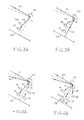
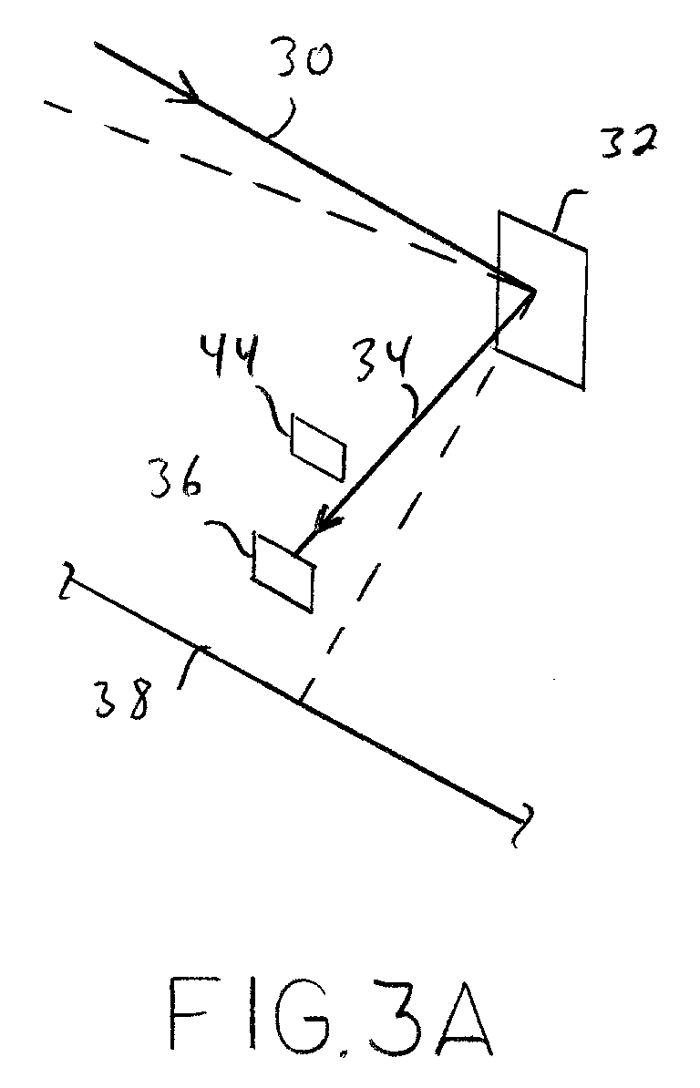
- an imaging system in accordance with an embodiment of the invention involves directing an illumination field 30 toward an illumination modulator 32 along an off-axis direction such that the zero order reflected illumination field 34 is directed toward an energy absorbing block filter 36 when the modulator is not activated. In this case, no illumination should be directed toward the imaging surface 38 when the modulator is not activated.
- the +/- first order reflected fields 40 and 42 are directed toward the imaging surface 38 and another energy absorbing block filter 44 respectively.
- the first order reflected field 40 is directed toward the imaging surface 38 along a direction that is normal to the surface 38.
- the reflected field 42 is not used in imaging, reducing throughput efficiency, the system provides a high contrast ratio.
- Another system of the invention may further include an additional illumination field 50 that is directed along an off-axis (e.g., a negative off-axis direction with respect to the field 30) toward the modulator 32 such that the zero order reflected illumination field 52 is directed toward an energy absorbing block filter 54 when the modulator is not activated as shown in Figure 4A. Again, no illumination should be directed toward the imaging surface 38 when the modulator is not activated.
- the +/- first order reflected fields 56 and 58 are directed toward the imaging surface 38 and another energy absorbing block filter 60 respectively.
- the first order reflected field 56 is coincident with the first order reflected field 40 and both are directed toward the imaging surface 38 along a direction that is normal to the surface 38.
- the system of Figures 4A and 4B may employ two independent illumination sources or may employ optics for splitting the illumination field from one illumination source to provide the illumination fields 30 and 50.
- the modulator may have a plurality of modulator elements along a horizontal direction across the modulator to provide a two first order reflections as shown in Figure 4A.
- Figures 5A and 5B show a further system of the invention similar to the system of Figure 4A and 4B in which the incident and reflected signals are coplanar.
- the system involves directing illumination fields 70 and 72 via beam splitters 74 and 76 toward an illumination modulator 78 along off-axis directions such that the zero order reflected illumination fields 80 and 82 are directed toward energy absorbing block filters 84 and 86 when the modulator is not activated as shown in Figure 5A. In this case, no illumination should be directed toward the imaging surface 88 when the modulator is not activated.
- the first order reflected fields 90 and 92 are directed toward the imaging surface 88 and the first order reflected fields 94 and 96 are directed toward energy absorbing block filters 98 and 100 respectively.
- the first order reflected fields 90 and 92 are coincident and are directed toward the imaging surface 88 along a direction that is normal to the surface 88. Again, although the reflected fields 94 and 96 are not used in imaging, the system provides a high contrast ratio.
- a benefit of using coplanar incident and reflected fields is that for illumination fields that are in the shape of a line, the coplanar system reduces any aberrations that may result in reflected fields when an incident field is directed toward the modulator from a high angle of incidence.
- Figure 6 shows an imaging system in which illumination fields 102 and 104 are directed via a field lens system 106 toward a GLV 108 having a grating spacing of, for example 8.5 ⁇ m .
- the illumination fields are each folded into collimated space at the GLV 108.
- the first order reflected fields from the GLV 108 are directed coincident with one another as shown at 110 and are directed through imaging optics 112 onto the imaging surface of an imaging drum 114.
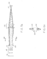
- Figures 7A and 7B show an illumination system in accordance with a further embodiment of the invention in which the modulator is off in Figure 7A and on in Figure 7B.
- the illumination system includes a plurality of illumination sources 120 that direct illumination via optics 122 through a broad mask 124 onto a modulator 126.
- the reflected illumination is dispersed in many directions, but when the modulator is turned on, the reflected illumination is directed via imaging optics 128 onto a surface 130 of an imageable medium as shown in Figure 7B.
- the system may include many illumination sources 120 that are positioned around the zero order direction (132).
- the system in effect, floods the modulator with illumination, but reflects only the illumination along the zero order using the imaging optics 128 as shown in Figure 8B.
- the illumination sources 120 may include one or more lens bars with a slow axis diffuser for single axis uniform angular diffusion.
- the illuminated line at the modulator may be broader than the active area and the mask without affecting the contrast ratio, although a loss of throughput may result.
- Figure 9 shows a side view of the imaging system of Figure 7B taken along line 9 - 9 in which the width of the imaging line on the modulator 126 and on the imaging surface 130 may be seen.
Landscapes
- Physics & Mathematics (AREA)
- General Physics & Mathematics (AREA)
- Optics & Photonics (AREA)
- Microscoopes, Condenser (AREA)
- Electronic Switches (AREA)
- Mechanical Light Control Or Optical Switches (AREA)
- Optical Modulation, Optical Deflection, Nonlinear Optics, Optical Demodulation, Optical Logic Elements (AREA)
- Optical Radar Systems And Details Thereof (AREA)
- Investigating Or Analysing Materials By Optical Means (AREA)
- Investigating Materials By The Use Of Optical Means Adapted For Particular Applications (AREA)
Abstract
Description
- The present invention relates to an imaging system empolying off-axis illumination of an illumination modulator.
- The invention generally relates to imaging systems, and relates in particular to imaging systems that employ an illumination modulator. Imaging systems such as those disclosed in U.S. Patent No. 6,433,934, may include an illumination source, a field lens system, an illumination modulator, imaging optics and an imaging surface. During imaging, the field lens system directs the illumination field onto the light modulator and the light modulator reflects the illumination field toward the imaging surface in one mode and reflects the illumination field away from the imaging surface in another mode. The modulator may, for example, include a Grating Light Valve (GLV) as sold by Silicon Light Machines of Sunnyvale, California, and the system may direct, via the imaging optics, either the zero order reflection or the first order reflection toward the imaging surface in various embodiments.
- In particular, the image may be recorded from the zero
order reflection 10 of theillumination field 12 from themodulator 14 at theimaging surface 16 as shown in Figure 1A during imaging. As shown in Figure 1B, when themodulator 14 is activated, theillumination field 12 is reflected atfirst order reflections 18A and 18B, and to a lesser extent at further order reflections (not shown). Thefirst order reflections 18A and 18B are blocked from reaching theimaging surface 16 by energy absorbingblocking filters 20A and 20B. Imaging occurs, therefore, when themodulator 14 is not activated as shown in Figure 1A. Ideally, no illumination should be directed along the path of the zero order reflection when themodulator 14 is activated as shown in Figure 1B. In practice, however, it may be difficult to completely remove illumination from the zero order direction. Theillumination field 12 andreflected fields - Another conventional imaging system may employ an energy absorbing
block filter 22 in the zeroorder direction 10 as shown in Figure 2A, and alens 24 to direct thefirst order reflections 18A and 18B toward theimaging surface 16 as shown in Figure 2B. Such an imaging system, however, requires very precise alignment of the components to ensure that thefirst order reflections 18A and 18B converge at a common focal point at theimaging surface 16. Any mis-alignment of these components may significantly reduce image quality. Further, off-axis imaging limits the available depth of focus in the imaging system. - Also, many imaging systems employ an illumination field that is generally in the shape of a line of illumination, permitting a line of picture elements (or pixels) to be imaged simultaneously. The
illumination fields modulator 14 and along theimaging surface 16 respectively. The use of an illumination field in the shape of a line may further complicate certain of the off-axis imaging constraints. - In certain applications it is desirable to provide an imaging system having a high contrast ratio that does not image when the power is not applied to the modulator, yet does not require highly precise alignment of numerous components and may be readily adjusted to optimum image quality.
- The above-mentioned problems are solved by a system having the specific features set out in
claim 1. Specific features for preferred embodiments of the invention are set out in the dependent claims. - The invention provides an imaging system that includes a first off-axis illumination source for providing an first illumination field at a surface of an illumination modulator such that when the modulator is in a first non-activated mode a zero-order reflected illumination field is directed toward a first illumination blocking device, and when the modulator is in a second activated mode one first order reflected illumination field is directed toward an imaging surface while another first order reflected illumination field is directed toward a second illumination blocking device in accordance with an embodiment.
- The imaging system may further include a second off-axis illumination source for providing a second illumination field at a surface of the illumination modulator such that when the modulator is in the first non-activated mode a zero-order second reflected illumination field is directed toward a second illumination blocking device, and when the modulator is in the second activated mode a first order second reflected illumination field is directed toward the imaging surface in accordance with a further embodiment of the invention.
- Further advantages and embodiments of the present invention will become apparent from the following description and drawings.
-
- Figures 1A and 1B show illustrative diagrammatic views of a prior art imaging system;
- Figures 2A and 2B show illustrative diagrammatic views of another prior art imaging system;
- Figures 3A and 3B show illustrative diagrammatic views of an imaging system in accordance with an embodiment of the invention;
- Figures 4A and 4B show illustrative diagrammatic views of an imaging system in accordance with another embodiment of the invention;
- Figures 5A and 5B show illustrative diagrammatic views of an imaging system in accordance with a further embodiment of the invention;
- Figure 6 shows an illustrative diagrammatic top view of an imaging system in accordance with another embodiment of the invention;
- Figures 7A and 7B show illustrative diagrammatic top views of an imaging system in accordance with a further embodiment of the invention;
- Figure 8A shows an illustrative diagrammatic end view of a portion
of the imaging system shown in Figure 7A taken along
line 8A - 8A thereof; - Figure 8B shows an illustrative diagrammatic end view of a portion of the imaging system shown in Figure 7B taken along line 8B - 8B thereof; and
- Figure 9 shows an illustrative diagrammatic side view of the imaging system shown in Figure 7B taken along line 9 - 9 thereof.
-
- The drawings are shown for illustrative purposes only and are not to scale.
- Systems of the invention may be used in a variety of imaging systems such as, for example, thermal imaging systems that include an illumination field, an illumination modulator and an imaging surface (e.g., an external imaging drum). The modulator receives the illumination field via a field lens system and directs a modulated illumination field toward the imaging surface via imaging optics. The illumination source, field lens system, modulator, imaging optics and imaging surface may be as disclosed in U.S. Patent No. 6,433,934, the disclosure of which is hereby incorporated by reference. The modulator may include a Grating Light Valve (GLV) as sold by Silicon Light Machines of Sunnyvale, California.
- As shown in Figure 3A, an imaging system in accordance with an embodiment of the invention involves directing an
illumination field 30 toward anillumination modulator 32 along an off-axis direction such that the zero order reflectedillumination field 34 is directed toward an energy absorbingblock filter 36 when the modulator is not activated. In this case, no illumination should be directed toward theimaging surface 38 when the modulator is not activated. During imaging as shown in Figure 3B, the +/- first order reflectedfields imaging surface 38 and another energy absorbingblock filter 44 respectively. The first order reflectedfield 40 is directed toward theimaging surface 38 along a direction that is normal to thesurface 38. Although thereflected field 42 is not used in imaging, reducing throughput efficiency, the system provides a high contrast ratio. - Another system of the invention may further include an
additional illumination field 50 that is directed along an off-axis (e.g., a negative off-axis direction with respect to the field 30) toward themodulator 32 such that the zero order reflectedillumination field 52 is directed toward an energy absorbingblock filter 54 when the modulator is not activated as shown in Figure 4A. Again, no illumination should be directed toward theimaging surface 38 when the modulator is not activated. During imaging as shown in Figure 4B, the +/- first order reflectedfields imaging surface 38 and another energy absorbingblock filter 60 respectively. The first order reflectedfield 56 is coincident with the first order reflectedfield 40 and both are directed toward theimaging surface 38 along a direction that is normal to thesurface 38. The system of Figures 4A and 4B may employ two independent illumination sources or may employ optics for splitting the illumination field from one illumination source to provide theillumination fields - Figures 5A and 5B show a further system of the invention similar to the system of Figure 4A and 4B in which the incident and reflected signals are coplanar. The system involves directing
illumination fields beam splitters illumination modulator 78 along off-axis directions such that the zero order reflectedillumination fields block filters imaging surface 88 when the modulator is not activated. During imaging as shown in Figure 5B, the first order reflectedfields imaging surface 88 and the first order reflectedfields block filters fields imaging surface 88 along a direction that is normal to thesurface 88. Again, although thereflected fields - Figure 6 shows an imaging system in which
illumination fields field lens system 106 toward a GLV 108 having a grating spacing of, for example 8.5 µ m . The illumination fields are each folded into collimated space at the GLV 108. During actuation, the first order reflected fields from theGLV 108 are directed coincident with one another as shown at 110 and are directed throughimaging optics 112 onto the imaging surface of animaging drum 114. - Figures 7A and 7B show an illumination system in accordance with a further embodiment of the invention in which the modulator is off in Figure 7A and on in Figure 7B. In particular, the illumination system includes a plurality of
illumination sources 120 that direct illumination viaoptics 122 through abroad mask 124 onto amodulator 126. When the modulator is off, the reflected illumination is dispersed in many directions, but when the modulator is turned on, the reflected illumination is directed viaimaging optics 128 onto asurface 130 of an imageable medium as shown in Figure 7B. As shown in Figure 8A, the system may includemany illumination sources 120 that are positioned around the zero order direction (132). The system, in effect, floods the modulator with illumination, but reflects only the illumination along the zero order using theimaging optics 128 as shown in Figure 8B. Theillumination sources 120 may include one or more lens bars with a slow axis diffuser for single axis uniform angular diffusion. The illuminated line at the modulator may be broader than the active area and the mask without affecting the contrast ratio, although a loss of throughput may result. Figure 9 shows a side view of the imaging system of Figure 7B taken along line 9 - 9 in which the width of the imaging line on themodulator 126 and on theimaging surface 130 may be seen. - Those skilled in the art will appreciate that numerous modifications and variations may be made to the above disclosed embodiments without departing from the spirit and scope of the invention.
Claims (9)
- An imaging system comprising:said imaging system being characterized in that:an off-axis illumination source for providing an illumination field (30) at a surface of an illumination modulator (32), said modulator having a first and a second mode;a first illumination blocking device (36);a second illumination blocking device (44);an imaging surface (38);when said modulator (32) is in said first mode, a zero-order reflected illumination field (34) is directed toward said first illumination blocking device (36);when said modulator (32) is in said second mode, a first first-order reflected illumination field (40) is directed toward said imaging surface (38) while a second first-order reflected illumination field (42) is directed toward said second illumination blocking device (44).
- An imaging system comprising:said imaging system being characterized in that:a first off-axis illumination source for providing a first illumination field (30) at a surface of an illumination modulator (32), said modulator having a first and a second mode;a second off-axis illumination source for providing a second illumination field (50) at said surface of said illumination modulator (32);a first illumination blocking device (36);a second illumination blocking device (44);a third illumination blocking device (54);a fourth illumination blocking device (60);an imaging surface (38);when said modulator (32) is in said first mode, a first zero-order reflected illumination field (34) is directed toward said first illumination blocking device (36) and a second zero-order reflected illumination filed (52) is directed towards said third illumination blocking device (54);when said modulator (32) is in said second mode, a first first-order reflected illumination field (40) and a second first-order reflected illumination field (56) are directed toward said imaging surface (38), while a third first-order reflected illumination field (42) is directed toward said second illumination blocking device (44) and a fourth first-order reflected illumination field (58) is directed toward said fourth illumination blocking device (60).
- The imaging system according to claim 2, wherein said first and second off-axis illumination fields are produced by a common illumination source.
- The imaging system according to anyone of the claims 2 or 3, wherein said first (40) first-order reflected illumination field is coincident with said second (56) first-order second reflected illumination field.
- The imaging system according to claim 1, wherein said first-order reflected illumination field (40) is directed toward the imaging surface along a direction that is normal to said modulator (32).
- The imaging system according to anyone of the previous claims, wherein said first mode is a non-activated mode and wherein said second mode is an activated mode.
- The imaging system according to anyone of the previous claims, wherein said first mode is a first activated mode and wherein said second mode is a second activated mode.
- The imaging system according to anyone of the previous claims, wherein the directions of said illumination field (70,72), said zero-order reflected illumination fields (80,82) and said first-order illumination fields (90,92) define a single plane.
- An imaging system according to the previous claim, wherein said illumination modulator (126) comprises modulator elements mutually spaced from one another along a direction that is orthogonal with regard to said single plane.
Applications Claiming Priority (2)
| Application Number | Priority Date | Filing Date | Title |
|---|---|---|---|
| US868528 | 2004-06-15 | ||
| US10/868,528 US7012766B2 (en) | 2004-06-15 | 2004-06-15 | Imaging system and method employing off-axis illumination of an illumination modulator |
Publications (2)
| Publication Number | Publication Date |
|---|---|
| EP1607225A2 true EP1607225A2 (en) | 2005-12-21 |
| EP1607225A3 EP1607225A3 (en) | 2008-10-08 |
Family
ID=35004299
Family Applications (1)
| Application Number | Title | Priority Date | Filing Date |
|---|---|---|---|
| EP05105249A Withdrawn EP1607225A3 (en) | 2004-06-15 | 2005-06-15 | Imaging system and method employing off-axis illumination of an illumination modulator |
Country Status (3)
| Country | Link |
|---|---|
| US (1) | US7012766B2 (en) |
| EP (1) | EP1607225A3 (en) |
| JP (1) | JP2006072322A (en) |
Citations (1)
| Publication number | Priority date | Publication date | Assignee | Title |
|---|---|---|---|---|
| US6433934B1 (en) | 2000-08-11 | 2002-08-13 | Yakov Reznichenko | Illumination system for use in imaging systems |
Family Cites Families (1)
| Publication number | Priority date | Publication date | Assignee | Title |
|---|---|---|---|---|
| US6411425B1 (en) * | 2000-09-27 | 2002-06-25 | Eastman Kodak Company | Electromechanical grating display system with spatially separated light beams |
-
2004
- 2004-06-15 US US10/868,528 patent/US7012766B2/en not_active Expired - Fee Related
-
2005
- 2005-06-08 JP JP2005168136A patent/JP2006072322A/en not_active Withdrawn
- 2005-06-15 EP EP05105249A patent/EP1607225A3/en not_active Withdrawn
Patent Citations (1)
| Publication number | Priority date | Publication date | Assignee | Title |
|---|---|---|---|---|
| US6433934B1 (en) | 2000-08-11 | 2002-08-13 | Yakov Reznichenko | Illumination system for use in imaging systems |
Also Published As
| Publication number | Publication date |
|---|---|
| EP1607225A3 (en) | 2008-10-08 |
| US20050275957A1 (en) | 2005-12-15 |
| JP2006072322A (en) | 2006-03-16 |
| US7012766B2 (en) | 2006-03-14 |
Similar Documents
| Publication | Publication Date | Title |
|---|---|---|
| US4251129A (en) | Photoelectric detecting device | |
| US4653880A (en) | Reflective beam splitting objective | |
| US4199219A (en) | Device for scanning an object with a light beam | |
| JP2975719B2 (en) | Confocal optics | |
| JPS6011325B2 (en) | scanning device | |
| JP7130625B2 (en) | Microscope for observing individually illuminated oblique planes with microlens array | |
| JPH07110451A (en) | Optical scanning device | |
| US4993792A (en) | Scanning optical system in which a ghost image is eliminated | |
| JPS63765B2 (en) | ||
| US7012766B2 (en) | Imaging system and method employing off-axis illumination of an illumination modulator | |
| JP2005031280A (en) | Exposure apparatus | |
| JPS62265613A (en) | Two-dimensional deflecting device for light beam | |
| US5191463A (en) | Scanning optical system in which a ghost image is elminated | |
| US6504137B1 (en) | Focusing system and method for use in imaging systems | |
| JP3048267B2 (en) | Microscope optics | |
| JP3290705B2 (en) | Confocal optics | |
| JP2003083723A (en) | Three-dimensional shape measuring optical system | |
| JP3362308B2 (en) | Integrated transmission and reception optical communication device | |
| US20250123368A1 (en) | Light emission module and wide angle scanning system | |
| EP1376194A3 (en) | Refracting element array, diffracting element array and exposure apparatus | |
| JP2001255480A (en) | Optical scanning device | |
| CA1318162C (en) | Arrangement for imaging multiple arrays of light beams | |
| JP2002031772A5 (en) | ||
| JPH0658464B2 (en) | Beam optical scanning optical device | |
| JPS5915216A (en) | optical scanning device |
Legal Events
| Date | Code | Title | Description |
|---|---|---|---|
| PUAI | Public reference made under article 153(3) epc to a published international application that has entered the european phase |
Free format text: ORIGINAL CODE: 0009012 |
|
| AK | Designated contracting states |
Kind code of ref document: A2 Designated state(s): AT BE BG CH CY CZ DE DK EE ES FI FR GB GR HU IE IS IT LI LT LU MC NL PL PT RO SE SI SK TR |
|
| AX | Request for extension of the european patent |
Extension state: AL BA HR LV MK YU |
|
| PUAL | Search report despatched |
Free format text: ORIGINAL CODE: 0009013 |
|
| AK | Designated contracting states |
Kind code of ref document: A3 Designated state(s): AT BE BG CH CY CZ DE DK EE ES FI FR GB GR HU IE IS IT LI LT LU MC NL PL PT RO SE SI SK TR |
|
| AX | Request for extension of the european patent |
Extension state: AL BA HR LV MK YU |
|
| RIC1 | Information provided on ipc code assigned before grant |
Ipc: G02B 26/08 20060101ALI20080901BHEP Ipc: B41J 2/465 20060101AFI20051013BHEP |
|
| 17P | Request for examination filed |
Effective date: 20090408 |
|
| AKX | Designation fees paid |
Designated state(s): DE FR GB |
|
| GRAP | Despatch of communication of intention to grant a patent |
Free format text: ORIGINAL CODE: EPIDOSNIGR1 |
|
| STAA | Information on the status of an ep patent application or granted ep patent |
Free format text: STATUS: THE APPLICATION IS DEEMED TO BE WITHDRAWN |
|
| 18D | Application deemed to be withdrawn |
Effective date: 20100415 |