EP1605685A1 - Image sensor with shared reset signal and row select - Google Patents
Image sensor with shared reset signal and row select Download PDFInfo
- Publication number
- EP1605685A1 EP1605685A1 EP04253371A EP04253371A EP1605685A1 EP 1605685 A1 EP1605685 A1 EP 1605685A1 EP 04253371 A EP04253371 A EP 04253371A EP 04253371 A EP04253371 A EP 04253371A EP 1605685 A1 EP1605685 A1 EP 1605685A1
- Authority
- EP
- European Patent Office
- Prior art keywords
- image sensor
- read
- floating diffusion
- reset voltage
- reset
- Prior art date
- Legal status (The legal status is an assumption and is not a legal conclusion. Google has not performed a legal analysis and makes no representation as to the accuracy of the status listed.)
- Granted
Links
- 238000009792 diffusion process Methods 0.000 claims abstract description 22
- 239000007787 solid Substances 0.000 claims description 13
- 239000003990 capacitor Substances 0.000 claims description 10
- 238000005286 illumination Methods 0.000 claims description 4
- 230000003287 optical effect Effects 0.000 description 4
- 241000699666 Mus <mouse, genus> Species 0.000 description 3
- 102100033118 Phosphatidate cytidylyltransferase 1 Human genes 0.000 description 2
- 101710178747 Phosphatidate cytidylyltransferase 1 Proteins 0.000 description 2
- 102100033126 Phosphatidate cytidylyltransferase 2 Human genes 0.000 description 2
- 101710178746 Phosphatidate cytidylyltransferase 2 Proteins 0.000 description 2
- 238000010586 diagram Methods 0.000 description 2
- 230000000694 effects Effects 0.000 description 2
- 238000000034 method Methods 0.000 description 2
- 239000000523 sample Substances 0.000 description 2
- 241000699670 Mus sp. Species 0.000 description 1
- 230000005540 biological transmission Effects 0.000 description 1
- 230000001413 cellular effect Effects 0.000 description 1
- 230000008878 coupling Effects 0.000 description 1
- 238000010168 coupling process Methods 0.000 description 1
- 238000005859 coupling reaction Methods 0.000 description 1
- 238000002347 injection Methods 0.000 description 1
- 239000007924 injection Substances 0.000 description 1
- 239000013074 reference sample Substances 0.000 description 1
- 238000005070 sampling Methods 0.000 description 1
Images





Classifications
-
- H—ELECTRICITY
- H04—ELECTRIC COMMUNICATION TECHNIQUE
- H04N—PICTORIAL COMMUNICATION, e.g. TELEVISION
- H04N25/00—Circuitry of solid-state image sensors [SSIS]; Control thereof
- H04N25/70—SSIS architectures; Circuits associated therewith
- H04N25/76—Addressed sensors, e.g. MOS or CMOS sensors
- H04N25/766—Addressed sensors, e.g. MOS or CMOS sensors comprising control or output lines used for a plurality of functions, e.g. for pixel output, driving, reset or power
-
- H—ELECTRICITY
- H04—ELECTRIC COMMUNICATION TECHNIQUE
- H04N—PICTORIAL COMMUNICATION, e.g. TELEVISION
- H04N25/00—Circuitry of solid-state image sensors [SSIS]; Control thereof
- H04N25/70—SSIS architectures; Circuits associated therewith
- H04N25/76—Addressed sensors, e.g. MOS or CMOS sensors
- H04N25/77—Pixel circuitry, e.g. memories, A/D converters, pixel amplifiers, shared circuits or shared components
- H04N25/778—Pixel circuitry, e.g. memories, A/D converters, pixel amplifiers, shared circuits or shared components comprising amplifiers shared between a plurality of pixels, i.e. at least one part of the amplifier must be on the sensor array itself
Definitions
- This invention relates to solid state image sensors, and is particularly but not exclusively useful in image sensors for use in mobile applications such as cellular phones.
- the invention also relates to devices, such as mobile phones, digital cameras and optical mice (computer pointing devices) incorporating solid state image sensors.
- Image sensors using pinned photodiode pixels are well known. Such image sensors in many applications have the advantage that both the image sensitive element and the image processing circuitry can be embodied in a single chip which can be manufactured using CMOS techniques.
- the present invention seeks to provide an image sensor which addresses these problems.
- the invention provides a solid state image sensor comprising an array of pixels arranged in rows and columns, each pixel having a pinned photodiode connected to a floating diffusion via a transfer gate, the floating diffusion providing an output to a column output line via a source follower.
- Each row has a transfer gate control line.
- the image sensor includes at least one read/reset voltage supply line connected to the floating diffusion via a read/reset transistor. The or each read/reset voltage supply line is driven by a decoder circuit at alternately a predetermined reset voltage and a substantially lower voltage.
- the invention further provides a digital camera, a mobile telephone, and a computer pointing device, each having such an image sensor.
- a pixel 10 of an image array has three horizontal lines: a reset line RST(j), a transfer gate line TG(j), and a read line RD(j), and two vertical lines: a reset voltage line VRT and a signal line Vx.
- VRT the reset potential of the floating diffusion FD
- VRT must supply current (typically a few mA) to bias the source followers at a sufficiently high voltage to cause complete charge transfer from the pinned photodiode without lag; typically the required voltage is around 3V.
- the supply voltage to the chip is often only 2.4-2.5V, and thus the 3V supply must be generated from a charge pump.
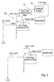
- an array of pixels 10 is supplied at 3V at 12 from a battery supply Vdd of 2.4V via a charge pump 14 and a voltage regulator 16 controlled by a bandgap voltage 18.
- the load current required to be delivered by the charge pump 14 determines the size of the pump capacitors, clock frequency, and efficiency. Often this necessitates a storage capacitor 20 of a size which can only be provided off-chip, which increases the system physical size and cost.
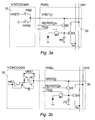
- FIG. 3 there is shown the operating principle of a single pixel 30 in one embodiment of the present invention.
- the pixel 30 operates as a pinned photodiode pixel using three transistors M1-M3, the floating diffusion being shown as a capacitor FD.
- Fig. 3a shows the Y-decoder circuit 32 schematically as an analog multiplexer.
- Fig. 3b shows the circuit 32 in the form of a level shifter.
- the timing of the pixel 30 is illustrated in Fig. 4.
- RD/RST(j) and rst(j) are maintained in these states by the Y-decoder 32 for all rows of pixels (j) which are not being read.
- the reset and signal voltages from the pixel are sampled by signals CDS1 and CDS2 at the base of the column.
- the RD/RST(j) line falls to 0V causing charge injection and reset coupling to produce a small decrease in the voltage on FD.
- the voltage on Vx follows this change and is sampled by CDS1 on a column capacitor. This sample is the black reference sample from the pixel.
- the sampled voltages are subtracted to remove kT/C noise introduced when releasing FD from reset.
- VRST still has to be typically 3V which can be produced by a charge pump 36 supplying a voltage regulator 38.
- Fig. 6 illustrates the voltage conditions on M3 during and after reset
- the invention thus makes it possible to dispense with off-chip storage elements. Further, the invention allows a pinned-photodiode arrangement which requires only three (or fewer) transistors per pixel.
- the senor may form part of a digital camera in which a camera lens focuses a desired image onto the image plane of the image sensor.
- the image sensor may be incorporated in a mobile phone having the customary receiving and transmitting means for digital signals.
- a further use is in an optical mouse, or pointing device, for use with a computer.
- the optical mouse has a housing which provides a button surface and which contains an illumination source, a lens, and a solid state image sensor.
- the lens provides optical transmission of highlights, produced by the illumination source on a mouse mat or equivalent to the image sensor.
- the invention is particularly suited to such applications, where efficient power supply arrangements are desirable to minimise current draw and battery size, and to prolong battery life.
Landscapes
- Engineering & Computer Science (AREA)
- Multimedia (AREA)
- Signal Processing (AREA)
- Solid State Image Pick-Up Elements (AREA)
- Transforming Light Signals Into Electric Signals (AREA)
Abstract
Description
Claims (14)
- A solid state image sensor comprising an array of pixels arranged in rows and columns, each pixel having a pinned photodiode connected to a floating diffusion via a transfer gate, the floating diffusion providing an output to a column output line via a source follower;
in which each row has a transfer gate control line;
and including at least one read/reset voltage supply line connected to the floating diffusion via a read/reset transistor, the or each read/reset voltage supply line being driven by a decoder circuit at alternately a predetermined reset voltage and a substantially lower voltage. - a solid state image sensor according to claim 1, in which said substantially lower voltage is between zero and a few hundred millivolts above ground.
- A solid state image sensor according to claim 1 or claim 2, in which each pixel includes a read/reset transistor and each row has a read/reset voltage supply line.
- A solid state image sensor according to claim 1 or claim 2, in which a number of pixels in a column share a common floating diffusion, an associated common read/reset transistor, and a common read/reset voltage supply line.
- An image sensor according to any preceding claim, in which said decoder circuit is an analog multiplexer.
- An image sensor according to any of claims 1 to 4, in which said decoder circuit is a level shifter.
- An image sensor according to any preceding claim, in which each column line is connected alternately to a black level store and a signal level store in synchronism with said read/reset voltages, and the stored values are subtracted to cancel kT/C noise.
- An image sensor according to claim 7, in which said stores are column capacitors.
- An image sensor according to any preceding claim, in which the read/reset voltage decoders are supplied with said predetermined reset voltage by a power supply circuit which includes a charge pump circuit, the charge pump circuit including any associated storage capacitors being entirely on-chip.
- An image sensor according to claim 9, in which the charge pump circuit includes an on-chip storage capacitor of about 20µF.
- An image sensor according to claim 9 or claim 10, in which power to the remainder of the image sensor is supplied by a second power supply circuit at a lower voltage than that of the charge pump.
- A digital camera having a solid state image sensor comprising an array of pixels arranged in rows and columns, each pixel having a pinned photodiode connected to a floating diffusion via a transfer gate, the floating diffusion providing an output to a column output line via a source follower;
in which each row has a transfer gate control line;
and including at least one read/reset voltage supply line connected to the floating diffusion via a read/reset transistor, the or each read/reset voltage supply line being driven by a decoder circuit at alternately a predetermined reset voltage and a substantially lower voltage. - A mobile telephone comprising receiving means and transmitting means for digital data and a solid state image sensor, the image sensor comprising an array of pixels arranged in rows and columns, each pixel having a pinned photodiode connected to a floating diffusion via a transfer gate, the floating diffusion providing an output to a column output line via a source follower;
in which each row has a transfer gate control line;
and including at least one read/reset voltage supply line connected to the floating diffusion via a read/reset transistor, the or each read/reset voltage supply line being driven by a decoder circuit at alternately a predetermined reset voltage and a substantially lower voltage. - A pointing device for a computer system comprising a housing having a button surface, a source of illumination mounted within the housing, and a solid state image sensor mounted within the housing and optically coupled by a lens to highlights originating from the illumination source;
and in which the solid state image sensor comprises an array of pixels arranged in rows and columns, each pixel having a pinned photodiode connected to a floating diffusion via a transfer gate, the floating diffusion providing an output to a column output line via a source follower;
in which each row has a transfer gate control line;
and including at least one read/reset voltage supply line connected to the floating diffusion via a read/reset transistor, the or each read/reset voltage supply line being driven by a decoder circuit at alternately a predetermined reset voltage and a substantially lower voltage.
Priority Applications (3)
| Application Number | Priority Date | Filing Date | Title |
|---|---|---|---|
| DE602004017969T DE602004017969D1 (en) | 2004-06-05 | 2004-06-05 | Image sensor with split reset signals and line selection |
| EP04253371A EP1605685B1 (en) | 2004-06-05 | 2004-06-05 | Image sensor with shared reset signal and row select |
| US11/144,112 US7830432B2 (en) | 2004-06-05 | 2005-06-03 | Image sensor for mobile use and associated methods |
Applications Claiming Priority (1)
| Application Number | Priority Date | Filing Date | Title |
|---|---|---|---|
| EP04253371A EP1605685B1 (en) | 2004-06-05 | 2004-06-05 | Image sensor with shared reset signal and row select |
Publications (2)
| Publication Number | Publication Date |
|---|---|
| EP1605685A1 true EP1605685A1 (en) | 2005-12-14 |
| EP1605685B1 EP1605685B1 (en) | 2008-11-26 |
Family
ID=34930377
Family Applications (1)
| Application Number | Title | Priority Date | Filing Date |
|---|---|---|---|
| EP04253371A Expired - Lifetime EP1605685B1 (en) | 2004-06-05 | 2004-06-05 | Image sensor with shared reset signal and row select |
Country Status (3)
| Country | Link |
|---|---|
| US (1) | US7830432B2 (en) |
| EP (1) | EP1605685B1 (en) |
| DE (1) | DE602004017969D1 (en) |
Cited By (4)
| Publication number | Priority date | Publication date | Assignee | Title |
|---|---|---|---|---|
| EP1944961A1 (en) * | 2007-01-12 | 2008-07-16 | STMicroelectronics (Research & Development) Limited | Image sensor power supply |
| WO2008108884A1 (en) | 2007-03-08 | 2008-09-12 | Imagerlabs, Inc. | Ultra low noise cmos imager |
| EP2180514A3 (en) * | 2008-10-22 | 2011-03-23 | Sony Corporation | Solid state image sensor, method for driving a solid state image sensor, imaging apparatus, and electronic device |
| EP2062434A4 (en) * | 2006-09-11 | 2011-08-17 | Siliconfile Technologies Inc | PIXEL COMPRISING THREE TRANSISTORS AND A PIXEL MATRIX CONTAINING PIXELS |
Families Citing this family (8)
| Publication number | Priority date | Publication date | Assignee | Title |
|---|---|---|---|---|
| JP4818018B2 (en) * | 2006-08-01 | 2011-11-16 | キヤノン株式会社 | Photoelectric conversion device and imaging system using the same |
| JP4979375B2 (en) * | 2006-12-28 | 2012-07-18 | キヤノン株式会社 | Solid-state imaging device and imaging system |
| JP5181982B2 (en) * | 2008-09-30 | 2013-04-10 | ソニー株式会社 | Solid-state imaging device and camera system |
| JP2010273158A (en) * | 2009-05-22 | 2010-12-02 | Toshiba Corp | Power supply noise elimination circuit |
| JP2012253544A (en) * | 2011-06-02 | 2012-12-20 | Toshiba Corp | Solid-state imaging device |
| KR102083776B1 (en) * | 2013-09-03 | 2020-04-16 | 삼성전자 주식회사 | Image sensor for supplying a different voltage to pixels based on illumination change, operation method thereof, and device having image sensor |
| EP3661192B1 (en) * | 2018-11-30 | 2022-10-05 | ams Sensors Belgium BVBA | Pixel drive voltage generation using a charge pump |
| US20220021830A1 (en) * | 2020-07-20 | 2022-01-20 | Novatek Microelectronics Corp. | Optical sensing device and method thereof |
Citations (6)
| Publication number | Priority date | Publication date | Assignee | Title |
|---|---|---|---|---|
| EP0905788A2 (en) * | 1997-09-29 | 1999-03-31 | Canon Kabushiki Kaisha | MOS type image sensing device |
| EP1017107A2 (en) * | 1998-12-30 | 2000-07-05 | Eastman Kodak Company | Photogate active pixel sensor with high fill factor and correlated double sampling |
| EP1017231A2 (en) * | 1998-12-30 | 2000-07-05 | Eastman Kodak Company | Photodiode active pixel sensor with shared reset signal and row select |
| EP1117249A2 (en) * | 1999-12-14 | 2001-07-18 | Omnivision Technologies Inc. | Improved active pixel sensor reset circuit for reducing image lag |
| EP1353500A2 (en) * | 2002-04-05 | 2003-10-15 | CSEM Centre Suisse d'Electronique et de Microtechnique | Image sensor |
| US20040069930A1 (en) * | 1998-03-16 | 2004-04-15 | Silicon Video, Inc. | Photo imager with shared reset FET and pixel amplifier |
Family Cites Families (7)
| Publication number | Priority date | Publication date | Assignee | Title |
|---|---|---|---|---|
| US6320616B1 (en) * | 1997-06-02 | 2001-11-20 | Sarnoff Corporation | CMOS image sensor with reduced fixed pattern noise |
| US6667768B1 (en) * | 1998-02-17 | 2003-12-23 | Micron Technology, Inc. | Photodiode-type pixel for global electronic shutter and reduced lag |
| US6140630A (en) * | 1998-10-14 | 2000-10-31 | Micron Technology, Inc. | Vcc pump for CMOS imagers |
| US7106357B2 (en) * | 2001-08-27 | 2006-09-12 | Olympus Optical Co., Ltd. | Portable information terminal device having camera feature |
| US20030076431A1 (en) * | 2001-10-24 | 2003-04-24 | Krymski Alexander I. | Image sensor with pixels having multiple capacitive storage elements |
| JP4132850B2 (en) * | 2002-02-06 | 2008-08-13 | 富士通株式会社 | CMOS image sensor and control method thereof |
| US20040001056A1 (en) * | 2002-06-28 | 2004-01-01 | Honeywell International Inc. | Electrochromic window driver |
-
2004
- 2004-06-05 DE DE602004017969T patent/DE602004017969D1/en not_active Expired - Fee Related
- 2004-06-05 EP EP04253371A patent/EP1605685B1/en not_active Expired - Lifetime
-
2005
- 2005-06-03 US US11/144,112 patent/US7830432B2/en active Active
Patent Citations (6)
| Publication number | Priority date | Publication date | Assignee | Title |
|---|---|---|---|---|
| EP0905788A2 (en) * | 1997-09-29 | 1999-03-31 | Canon Kabushiki Kaisha | MOS type image sensing device |
| US20040069930A1 (en) * | 1998-03-16 | 2004-04-15 | Silicon Video, Inc. | Photo imager with shared reset FET and pixel amplifier |
| EP1017107A2 (en) * | 1998-12-30 | 2000-07-05 | Eastman Kodak Company | Photogate active pixel sensor with high fill factor and correlated double sampling |
| EP1017231A2 (en) * | 1998-12-30 | 2000-07-05 | Eastman Kodak Company | Photodiode active pixel sensor with shared reset signal and row select |
| EP1117249A2 (en) * | 1999-12-14 | 2001-07-18 | Omnivision Technologies Inc. | Improved active pixel sensor reset circuit for reducing image lag |
| EP1353500A2 (en) * | 2002-04-05 | 2003-10-15 | CSEM Centre Suisse d'Electronique et de Microtechnique | Image sensor |
Cited By (9)
| Publication number | Priority date | Publication date | Assignee | Title |
|---|---|---|---|---|
| EP2062434A4 (en) * | 2006-09-11 | 2011-08-17 | Siliconfile Technologies Inc | PIXEL COMPRISING THREE TRANSISTORS AND A PIXEL MATRIX CONTAINING PIXELS |
| EP1944961A1 (en) * | 2007-01-12 | 2008-07-16 | STMicroelectronics (Research & Development) Limited | Image sensor power supply |
| US8120700B2 (en) | 2007-01-12 | 2012-02-21 | Stmicroelectronics (Research & Development) Limited | Image sensor power supply |
| WO2008108884A1 (en) | 2007-03-08 | 2008-09-12 | Imagerlabs, Inc. | Ultra low noise cmos imager |
| EP2135443A4 (en) * | 2007-03-08 | 2011-12-21 | Imagerlabs Inc | VERY LOW NOISE CMOS IMAGER |
| EP2180514A3 (en) * | 2008-10-22 | 2011-03-23 | Sony Corporation | Solid state image sensor, method for driving a solid state image sensor, imaging apparatus, and electronic device |
| US8570412B2 (en) | 2008-10-22 | 2013-10-29 | Sony Corporation | Solid state image sensor, method for driving a solid state image sensor, imaging apparatus, and electronic device |
| US9247172B2 (en) | 2008-10-22 | 2016-01-26 | Sony Corporation | Solid state image sensor, method for driving a solid state image sensor, imaging apparatus, and electronic device |
| US9781371B2 (en) | 2008-10-22 | 2017-10-03 | Sony Corporation | Solid state image sensor, method for driving a solid state image sensor, imaging apparatus, and electronic device |
Also Published As
| Publication number | Publication date |
|---|---|
| EP1605685B1 (en) | 2008-11-26 |
| US20050269607A1 (en) | 2005-12-08 |
| US7830432B2 (en) | 2010-11-09 |
| DE602004017969D1 (en) | 2009-01-08 |
Similar Documents
| Publication | Publication Date | Title |
|---|---|---|
| KR101705491B1 (en) | Solid-state image pickup apparatus, signal processing method for a solid-state image pickup apparatus, and electronic apparatus | |
| KR101095720B1 (en) | Display device including an image sensor | |
| US8618589B2 (en) | Solid-state imaging device and driving method therefor | |
| US7595827B2 (en) | Imaging device | |
| CN206993236U (en) | A kind of imaging sensor and system | |
| US20220060647A1 (en) | Cds circuit, operating method thereof, and image sensor including cds circuit | |
| US11438530B2 (en) | Pixel unit with a design for half row reading, an imaging apparatus including the same, and an imaging method thereof | |
| US10277856B2 (en) | Solid-state imaging device, method for driving solid-state imaging device, and electronic apparatus | |
| JP7029698B2 (en) | Imaging device | |
| US9319612B2 (en) | Imagers with improved analog-to-digital circuitry | |
| US8411184B2 (en) | Column output circuits for image sensors | |
| US20160105624A1 (en) | Imaging device, imaging system, and method for driving imaging device | |
| US12418735B2 (en) | Solid-state imaging device, method for driving solid-state imaging device, and electronic apparatus | |
| EP1605685B1 (en) | Image sensor with shared reset signal and row select | |
| US8724002B2 (en) | Imaging pixels with dummy transistors that reduce reset charge injection | |
| US10630897B2 (en) | Image sensors with charge overflow capabilities | |
| CN119183033A (en) | Image sensor, operation method thereof, and electronic device | |
| US20090115878A1 (en) | Method, system and apparatus to boost pixel floating diffusion node voltage | |
| US10153318B2 (en) | Image sensor device with first and second source followers and related methods | |
| US9918029B2 (en) | Imaging systems with switchable column power control | |
| KR100621558B1 (en) | CMOS image sensor and its driving method | |
| JP2020114020A (en) | Image sensor and image-capturing device | |
| KR100690883B1 (en) | Image sensor | |
| CN116018819A (en) | Detection device | |
| KR20090015286A (en) | Image sensor and its driving method |
Legal Events
| Date | Code | Title | Description |
|---|---|---|---|
| PUAI | Public reference made under article 153(3) epc to a published international application that has entered the european phase |
Free format text: ORIGINAL CODE: 0009012 |
|
| AK | Designated contracting states |
Kind code of ref document: A1 Designated state(s): AT BE BG CH CY CZ DE DK EE ES FI FR GB GR HU IE IT LI LU MC NL PL PT RO SE SI SK TR |
|
| AX | Request for extension of the european patent |
Extension state: AL HR LT LV MK |
|
| 17P | Request for examination filed |
Effective date: 20060515 |
|
| 17Q | First examination report despatched |
Effective date: 20060721 |
|
| AKX | Designation fees paid |
Designated state(s): DE FR GB IT |
|
| GRAP | Despatch of communication of intention to grant a patent |
Free format text: ORIGINAL CODE: EPIDOSNIGR1 |
|
| GRAS | Grant fee paid |
Free format text: ORIGINAL CODE: EPIDOSNIGR3 |
|
| RAP1 | Party data changed (applicant data changed or rights of an application transferred) |
Owner name: STMICROELECTRONICS (RESEARCH & DEVELOPMENT) LIMITE |
|
| GRAA | (expected) grant |
Free format text: ORIGINAL CODE: 0009210 |
|
| AK | Designated contracting states |
Kind code of ref document: B1 Designated state(s): DE FR GB IT |
|
| REG | Reference to a national code |
Ref country code: GB Ref legal event code: FG4D |
|
| REF | Corresponds to: |
Ref document number: 602004017969 Country of ref document: DE Date of ref document: 20090108 Kind code of ref document: P |
|
| PLBE | No opposition filed within time limit |
Free format text: ORIGINAL CODE: 0009261 |
|
| STAA | Information on the status of an ep patent application or granted ep patent |
Free format text: STATUS: NO OPPOSITION FILED WITHIN TIME LIMIT |
|
| 26N | No opposition filed |
Effective date: 20090827 |
|
| PG25 | Lapsed in a contracting state [announced via postgrant information from national office to epo] |
Ref country code: DE Free format text: LAPSE BECAUSE OF NON-PAYMENT OF DUE FEES Effective date: 20100101 |
|
| PG25 | Lapsed in a contracting state [announced via postgrant information from national office to epo] |
Ref country code: IT Free format text: LAPSE BECAUSE OF FAILURE TO SUBMIT A TRANSLATION OF THE DESCRIPTION OR TO PAY THE FEE WITHIN THE PRESCRIBED TIME-LIMIT Effective date: 20081126 |
|
| REG | Reference to a national code |
Ref country code: FR Ref legal event code: PLFP Year of fee payment: 13 |
|
| REG | Reference to a national code |
Ref country code: FR Ref legal event code: PLFP Year of fee payment: 14 |
|
| REG | Reference to a national code |
Ref country code: FR Ref legal event code: PLFP Year of fee payment: 15 |
|
| PGFP | Annual fee paid to national office [announced via postgrant information from national office to epo] |
Ref country code: FR Payment date: 20230523 Year of fee payment: 20 |
|
| PGFP | Annual fee paid to national office [announced via postgrant information from national office to epo] |
Ref country code: GB Payment date: 20230523 Year of fee payment: 20 |
|
| REG | Reference to a national code |
Ref country code: GB Ref legal event code: PE20 Expiry date: 20240604 |
|
| PG25 | Lapsed in a contracting state [announced via postgrant information from national office to epo] |
Ref country code: GB Free format text: LAPSE BECAUSE OF EXPIRATION OF PROTECTION Effective date: 20240604 |
|
| PG25 | Lapsed in a contracting state [announced via postgrant information from national office to epo] |
Ref country code: GB Free format text: LAPSE BECAUSE OF EXPIRATION OF PROTECTION Effective date: 20240604 |