EP1605468A1 - Semiconductor memory - Google Patents
Semiconductor memory Download PDFInfo
- Publication number
- EP1605468A1 EP1605468A1 EP03715371A EP03715371A EP1605468A1 EP 1605468 A1 EP1605468 A1 EP 1605468A1 EP 03715371 A EP03715371 A EP 03715371A EP 03715371 A EP03715371 A EP 03715371A EP 1605468 A1 EP1605468 A1 EP 1605468A1
- Authority
- EP
- European Patent Office
- Prior art keywords
- cell
- guarantee
- data
- memory device
- semiconductor memory
- Prior art date
- Legal status (The legal status is an assumption and is not a legal conclusion. Google has not performed a legal analysis and makes no representation as to the accuracy of the status listed.)
- Granted
Links
Images






Classifications
-
- G—PHYSICS
- G11—INFORMATION STORAGE
- G11C—STATIC STORES
- G11C11/00—Digital stores characterised by the use of particular electric or magnetic storage elements; Storage elements therefor
- G11C11/21—Digital stores characterised by the use of particular electric or magnetic storage elements; Storage elements therefor using electric elements
- G11C11/22—Digital stores characterised by the use of particular electric or magnetic storage elements; Storage elements therefor using electric elements using ferroelectric elements
Definitions
- the present invention is made to solve such problems, and an object thereof is to securely retain data as nonvolatile binary data regardless of operating condition in a nonvolatile semiconductor memory device which has an operating condition involving destruction of data, thereby suppressing loss of data.
- the read data when a minute potential of the bit line generated by the data read out from the memory cell is amplified by a sense amplifier, the read data can be simultaneously written to the guarantee cell automatically, so that the data to be destroyed by reading can be securely retained until a restore operation is completed.
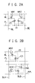
- Fig. 2B is a diagram showing a configuration example of a memory cell (1T/1C type cell) of the ferroelectric memory.
- a memory cell 22 and a reference cell 23 for outputting a reference potential are constituted of N-channel MOS transistors (transfer gates) MN3, MN4, and ferroelectric capacitors C3, C4, respectively.
- the ferroelectric memory has the same memory cell structure as a DRAM, which can be highly integrated similarly to the DRAM.
- the DRAM retains data by storing an electric charge in a dielectric capacitor.
- a transfer gate is opened (turned to an ON state)
- a minute potential corresponding to data is generated on a bit line by the electric charge discharged from the dielectric capacitor, and this minute potential is amplified by a sense amplifier to retrieve data "1", "0".
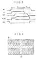
- Fig. 5 is a block diagram showing a configuration example of the bank 41 shown in Fig. 4.
- the bank 41 is constituted of two blocks 51 -A , 51 -B , a word line drive circuit 52, control circuits 53 -A , 53 -B and switches 54 -A , 54 -B provided corresponding to the blocks 51 -A , 51 -B respectively.
- the word line drive circuit 52 selectively activates word lines MWLj, SWL according to a decode result of the address information or the like.
- a memory cell is provided at each intersection of the word lines MWLj and the plate lines MPLj -A and the bit lines, and a guarantee cell is provided at each intersection of the word line SWL and the plate line SPL -A and the bit lines.
- the plate lines MPLj -A , MPLj -B of both the blocks will not be activated at the same time.
- all the plate lines in the other block are in an inactive state.
- active block the block in which the plate lines are activated
- sep block the block in which all the plate lines retain the inactive state
- BLi, /BLi are bit lines
- MWLj, SWL are word lines
- MPLj, SPL are plate lines
- PRC is a precharge signal line
- CL is a column signal line
- DBi, /DBi are data signal lines connected to a data bus
- PSA, NSA are control signal lines.
- the memory cells 61 have the same configuration except that they are connected to the different word lines MWLj and plate lines MPLj, the configuration will be described with reference to the memory cell 61 which is connected to a word line MWL1 and a plate line MPL1.
- the guarantee cell 62 is configured similarly to the memory cell 61 and constituted of two N-channel MOS transistors (transfer gates) MN7, MN8 and two ferroelectric capacitors C7, C8.
- One electrodes of the ferroelectric capacitors C7, C8 are connected to the bit lines BLi, /BLi via the transistors MN7, MN8 whose gates are connected to the word line SWL, and the other electrodes are connected to the plate line SPL.
- each column unit 56 has only one guarantee cell 62
- the gates of the transistors MN7, MN8 may be connected to the power supply voltage VDD with the guarantee cell 62 being configured as shown in Fig. 6.
- signal lines to which the bit lines BLi, /BLi are connected via the transistors MN11, MN12 are not the data signal lines DBi, /DBi but guarantee flag signal lines for setting the guarantee flag, and the rest of which has the same configuration as the column unit 56, so that the description thereof is omitted.
- the address information is retained in the guarantee cell.
- the loss of the address information can be prevented, but it is conceivable that the circuit configuration becomes complicated or the time needed for processing of access becomes long (an access cycle becomes slow) since the address information should be written to the guarantee cell before access to the memory cell is carried out.
- a nonvolatile ferroelectric latch circuit is provided in an address buffer unit 71 to which address information PAD is inputted externally, and the address information is retained in the address buffer unit 71 not by the guarantee cell but by the ferroelectric latch circuit and is supplied to a bank (block) as necessary.
- the transistors MP3 and MN15 and the transistors MP4 and MN16 constitute inverters respectively, and these two inverters are cross-coupled to constitute an SRAM (Static Random Access Memory) cell.
- SRAM Static Random Access Memory
- One input/output node of the SRAM cell is connected to a signal line SX via the transistor MN18 whose gate is connected to a signal line SCL, and the other input/output node is connected to a signal line SZ via the transistor MN19 whose gate is connected to the signal line SCL. Further, the signal lines SX, SZ are connected to the ground via the transistors MN20, MN21 whose gates are connected to a reset signal line RST. Incidentally, the signal lines SX, SZ are signal lines in a complementary relationship.
- One electrodes of the ferroelectric capacitors C10, C12 are connected commonly to the one input/output node of the SRAM cell, and one electrodes of the ferroelectric capacitors C11, C13 are connected commonly to the other input/output node of the SRAM cell. Further, the other electrodes of the ferroelectric capacitors C10, C11 are connected to the ground, and the other electrodes of the ferroelectric capacitors C12, C13 are connected to the signal line SPL.
- ferroelectric latch circuit To the ferroelectric latch circuit shown in Fig. 8, an output of a latch circuit of a not-shown address buffer which latches inputted address information is inputted. Further, the ferroelectric latch circuit is needed to be initialized once before usage in order to set the ferroelectric capacitors C10, C11 to be load capacitors to a predetermined state.
- Initialization in the ferroelectric latch circuit is performed such that, in a state that the power supply to the SRAM cell is cut off, the power supply voltage VDD is applied to the input/output nodes of the SRAM cell by the signal lines SX, SZ and the like, and thereafter they are discharged to the ground level.
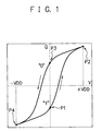
- the state of the ferroelectric capacitors C10, C11 transit on a linear term (linear region, which is the region between the point P1 and the point P4 shown in Fig. 1 (not including the other points)) which is not accompanied by a switching operation (inversion of polarization).
- Fig. 9 is a timing chart showing a write operation in the ferroelectric latch circuit shown in Fig. 8.
- Fig. 10 is a timing chart showing a read operation in the ferroelectric latch circuit shown in Fig. 8.
- the potentials of the signal lines PND, NND change respectively to "L”, "H” to supply power to the SRAM cell (at time T101 in Fig. 10), which makes the SRAM cell to act as a sense amplifier to amplify the potential of the input/output nodes of the SRAM cell. Accordingly, the potentials of the input/output nodes of the SRAM cell become the power supply voltage or the ground level.
- the potentials of the input/output nodes of the SRAM cell are transmitted to the signal lines SX, SZ via the transistors MN18, MN19, and thus data retained as potentials ADD' of the signal lines SX, SZ is read out.
- ferroelectric latch circuit shown in Fig. 8 is just an example and is not limited to this. Further, the circuit provided in the address buffer unit 71 for retaining the address information is not limited to the ferroelectric latch circuit, which may be any nonvolatile latch circuit.
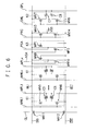
- Fig. 11 is a timing chart showing a reading sequence of data in the ferroelectric memory according to the first embodiment.
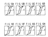
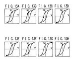
- Fig. 12A to Fig. 12H, and Fig. 13A to Fig. 13H are diagrams for describing polarization states of the ferroelectric capacitors of the memory cell and the guarantee cell during the reading sequence of data, respectively.
- the word line MWL, the plate line MPL, the bit lines BL, /BL and so on are word line, plate line, bit lines and so on connected to a memory cell from which data is to be read.
- ⁇ denotes a polarization state of the ferroelectric capacitor retaining the data "0”
- ⁇ denotes a polarization state of the ferroelectric capacitor retaining the data "1”.
- ⁇ and ⁇ denote polarization states of the ferroelectric capacitors connected to the same bit lines as the ferroelectric capacitors retaining the data "0" and the data "1" respectively.
- the guarantee flag is set before starting access to the memory cell in the memory device (ferroelectric memory).
- the bit lines to which the guarantee flag cell is connected are precharged to the power supply voltage VDD to write the data "1" in the guarantee flag cell.
- the potential of the precharge signal line PRC becomes "H” to precharge the bit lines BL, /BL to the ground level. Thereafter, the potential of the precharge signal line PRC is deactivated to "L", which changes the bit lines BL, /BL to a floating state.
- the polarization states of the ferroelectric capacitors of the memory cell and the guarantee cell in this initial state are as shown in Fig. 12A, Fig. 13A.
- the memory cell retains data, and the two ferroelectric capacitors in the memory cell are in different polarization states from each other which correspond to the data "1" and the data "0" respectively (refer to Fig. 12A).
- the guarantee cell is not needed to retain data in the initial state, which is just needed to operate so as to allow writing of data when the data is read out from the memory cell, so that the two ferroelectric capacitors in the guarantee cell are in the polarization state corresponding to the data "0" (refer to Fig. 13A).
- the reason why the initial state of the guarantee cell is a state of retaining the data "0" is to reduce time required for driving the plate line SPL so as to enable writing of data in the guarantee cell with the potential of the plate line SPL being "L".
- the state of retaining the data "0" is set as the initial state of the guarantee cell so that the data "1" will be automatically written to the guarantee cell when the potentials of the bit lines transit to the power supply voltage.
- Fig. 12C time T3
- Fig. 12D time T4
- a voltage is applied in a direction from the bit lines BL, /BL side to the plate line SPL side.
- the applied voltage becomes equal to or higher than a predetermined voltage
- the polarization direction of the ferroelectric capacitor is inverted to change from the initial state of retaining the data "0" to a state of retaining the data "1".
- the ferroelectric capacitor of the guarantee cell connected to the bit line that transits to the ground level maintains the initial state since the applied voltage is very low (refer to Fig. 13C, Fig. 13D showing the polarization states at time T3, T4).
- the data retained by the two ferroelectric capacitors of the guarantee cell is the same as the data retained by the ferroelectric capacitors of the memory cell before reading out. Therefore, in the ferroelectric memory that is destructive reading, the data retained in the memory cell before reading out can be securely retained not in an unstable state by an electric charge but in a stable state.
- the ferroelectric capacitors of the guarantee cell are in polarization states as shown in Fig. 13F.
- the restore operation is completed, the data retained in the guarantee cell becomes unnecessary, and thus the guarantee cell has to be returned to the initial state to be capable of responding to operations such as next reading of data from the memory cell or the like.
- the state of the guarantee cell after the restore operation is completed is the same state as the memory cell before reading, and the initial state of the guarantee cell is almost the same as the state of the memory cell at the time that the data reading operation is completed. Therefore, the guarantee cell can be initialized by the same method as the reading of data from the memory cell.
- the plate line SPL is turned to "H".
- the ferroelectric capacitors of the guarantee cell discharge an electric charge and change to the state of retaining the data "0" as shown in Fig. 13G, and thereafter the word line SWL and the plate line SPL are turned to "L".
- the ferroelectric capacitors of the guarantee cell return to the initial state as shown in Fig. 13H.
- the guarantee cell performs initialization while the bit lines BL, /BL are precharged to the ground level, thereby suppressing increase of time required for processing.
- bit lines BL, /BL are not in the floating state and are clamped to the ground level. At this time, no change of polarization state occurs in the memory cell as shown in Fig. 12G, Fig. 12H.
- the guarantee flag is initialized (changed to the data "0") after access (the read operation and the restore operation) to the memory cell is completed. Since the guarantee flag cell is connected to the same word line and plate line SPL as the guarantee cell, the guarantee flag is initialized automatically at the same time as the guarantee cell by the above-described initialization operation of the guarantee cell.
- the guarantee cell 62 is provided on the bit lines BL, /BL to which the memory cells 61 are connected, and when the minute potentials on the bit lines BL, /BL generated by the data read out from the memory cell 61 are amplified by the sense amplifier 63, the read data is written at the same time to the guarantee cell 62 by the amplified potentials of the bit lines BL, /BL.
- the data retaining function in the ferroelectric memory is improved, the period in which the retaining state of data is unstable is reduced, and the destructively read data can be securely retained as nonvolatile binary data. Accordingly, even when a contingency occurs before the restore operation in which the data read out from the memory cell 61 is written back to the memory cell is completed, loss of the read data can be suppressed. Further, requirements for power supply can be alleviated, and capacitors for power supply provided in the conventional ferroelectric memory for preventing loss of data due to a power cut-off can be reduced, which suppresses increase in chip area and allows efficient use of chip or miniaturization of chip.
- the ferroelectric memory according to the first embodiment While in a state that the reading and writing sequences abnormally finish due to a power cut-off or the like and the data in the memory cell is destroyed, the ferroelectric memory according to the first embodiment writes data from the guarantee cell to the memory cell in the startup operation after the power is turned on.
- the writing process of data from the guarantee cell to the memory cell in the startup operation depends on a storing method of the address information, so that the following description will be divided into the case of storing the address information in the guarantee cell and the case of storing it in a nonvolatile latch circuit as shown in Fig. 7 and Fig. 8.
- Fig. 14 is a flowchart showing an example of the startup operation in the ferroelectric memory according to the first embodiment.
- step S1 When the power is turned on in the memory device (ferroelectric memory), it is judged whether a self check flag is "0" or not in step S1. Here, an initial value of the self check flag after turning on the power is "0". Therefore, the operation mode of the memory device transits to a self check mode.
- the memory device is configured not to accept any control from the outside when the memory device is operating in the self check mode. Further, in order to notify that the operation mode is the self check mode to an external controller or the like, the memory device may be configured to output a signal denoting that it is in the self check mode (for example, a signal using the self check flag) to the outside.
- a signal denoting that it is in the self check mode for example, a signal using the self check flag
- step S2 reading of the guarantee block is performed in step S2.
- the address of the guarantee cell (a local address in the memory device) is specified to be the same as that for reading data from the memory cell, and then the word line SWL and the plate line SPL are activated to allow reading of data from the guarantee cell in the active block.
- the address of the guarantee cell is different from a normal address such as the address of the memory cell, which is for example an address in an address region to which access from the outside is prohibited, in order to prevent destruction of data by wrong access to the guarantee cell. Therefore, a decode logic for accessing the guarantee cell and a decode logic for accessing the memory cell are independent from each other, and thus the word lines MWL, SWL are independently controllable. With this configuration, usability thereof is improved, and an advantaged that double selection and activation of the word lines can be prevented is obtained.
- the data read from the guarantee cell is amplified by the sense amplifier and maintained on the bit lines BL, /BL. Further, a guarantee flag and address information are read from the guarantee cell in the sleep block and amplified by the sense amplifier, and thereafter the address information is outputted to the internal address bus ADB to initialize the guarantee cell in the sleep block. Incidentally, judgment of whether it is in the active block or the sleep block is done according to the value of the guarantee flag.
- step S3 the value of the self check flag is set to "1", and the flow returns to step S1. According to the result of judgment in step S1, the flow goes to step S4, which judges whether the value of the guarantee flag is "1" or not, in other words, the restore operation is completed or not. If the value of the guarantee flag is "0" as a result of the judgment in step S4, the process is terminated and a normal operation is started.
- step S4 if the value of the guarantee flag is "1" as a result of the judgment in step S4, the word line and plate line corresponding to the memory cell in which data is destroyed are selectively activated based on a decode result of the address information obtained in step S2.
- the data read out from the guarantee cell and retained in the bit lines BL, /BL is written to the memory cell to thereby complete the restoration of the destroyed data, and thus the normal operation is started.
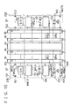
- Fig. 15 is a diagram showing a concrete configuration example of a bank in the ferroelectric memory in the case of storing the address information in the guarantee cell.
- Fig. 15 denotes a plate line drive circuit
- 56 denote column units for retaining data
- 57 denote column units for retaining a guarantee flag.
- the column units 57 are each connected to bit lines BL1, /BL1 (BL2, /BL2) and have a plurality of memory cells 151 controlled by word lines MWLj and plate lines MPL1j (MPL2j), a guarantee cell 152 controlled by a word line SWL and a plate line SPL1 (SPL2), and a sense amplifier 153.
- bit lines BL1, /BL1 (BL2, /BL2) and guarantee flag signal lines FG1, /FG1 (FG2, /FG2) are connected via N-channel MOS transistors MN22, MN23 whose gates are connected to a column signal line CL1 (CL2). Further, the bit lines BL1, /BL1 (BL2, /BL2) are connected to the ground via N-channel MOS transistors MN24, MN25 whose gates are connected to precharge control signal lines SPR1 (SPR2), and to the bit line BL1 (BL2), a guarantee flag output line SF1 (SF2) is further connected.
- bit lines BL1, /BL1 BL2, /BL2
- N-channel MOS transistors MN26, MN27 whose gates are connected to an address control line ADCT1 (ADCT2) are provided.
- the column units 56 are each configured similarly to the column unit 57.
- Bit lines BL, /BL included in the column units 56 are connected to an address bus ADB via transistors MN26, MN27 whose gates are connected to the address control line ADCT1 (ADCT2), and are connected to a data bus DTB via transistors MN22, MN23 whose gates are connected to the column signal line CL1 (CL2).
- Fig. 16 is a circuit diagram showing an example of a circuit generating potentials (address control signals) of the address control lines ADCT1, ADCT2 shown in Fig. 15.
- SF1, SF2 are guarantee flag output lines
- SCHK is a signal line outputting a potential related to the value of the self check flag
- BS1, BS2 are block selection signal lines.
- the signal line SCHK is "H” when the operation mode is the self check mode, and otherwise (normal operation) it is “L”.
- the block selection signal lines BS1, BS2 are "H” when the block is selected, in other words, when it is an active block, and otherwise it is "L".
- the guarantee flag output line SF1 and the signal line SCHK are each connected to input terminals of a negative logical product operation circuit (NAND circuit) 161.
- An output terminal of the NAND circuit 161 is connected to one input terminal of a negative logical sum operation circuit (NOR circuit) 163 via an inverter 162.
- NOR circuit negative logical sum operation circuit
- the address control line ADCT1 is configured identically using the guarantee flag line SF2, the signal line SCHK, and the block selection signal line BS1 and by a NAND circuit 165, inverters 166, 168 and a NOR circuit 167, and therefore the description of which is omitted.
- Fig. 17 is a circuit diagram showing an example of a circuit generating potentials of the precharge control signal lines SPR1, SPR2 shown in Fig. 15.
- SF1, SF2 are guarantee flag output lines
- /SCHK is a signal line outputting a potential related to a logically inverted value of the value of the self check flag
- PRC is a precharge signal line
- SAE is a sense amplifier signal line.
- the signal line /SCHK is "L" when the operation mode is the self check mode, and otherwise (normal operation mode) it is "H”.
- the guarantee flag output line SF1 is connected, and to the other input terminal thereof, the sense amplifier signal line SAE is connected.
- the precharge signal line PRC is connected, and to the other input terminal thereof, an output terminal of the AND circuit 179 is connected via a signal line SFC 1.
- the precharge signal line PRC is connected, and to the other input terminal thereof, the signal line /SCHK is connected.
- the precharge control signal line SPR2 is configured identically using the precharge signal line PRC, the guarantee flag output line SF2, the sense amplifier signal line SAE, and the signal line /SCHK, and by AND circuits 180, 175, 176, a NOR circuit 177, and an inverter 178, and therefore the description of which is omitted.
- Fig. 18 is a timing chart showing a startup operation in the ferroelectric memory shown in Fig. 15.
- a block on the side having bit lines BLS, /BLS and a guarantee flag output line SFS is explained as a sleep block
- a block on the side having bit lines BLA, /BLA and a guarantee flag output line SFA is explained as an active block.
- the potential of the precharge signal line becomes "L” again, and writing of data from the guarantee cell to the memory cell and initializing of the guarantee cell are performed after time T11.
- a potential of a word line WLx is selectively turned to "H” based on the address signal ADD
- the potential of the sense amplifier signal line SAE becomes "H”.
- a potential of a plate line PLx is selectively turned to "H", which turns to "L” after a predetermined period passes. Accordingly, the potentials of the bit lines BLA, /BLA according to data read out from the guarantee cell on the active block side are used to write the data "0" and the data "1" to the memory cell respectively, thereby restoring destroyed data.
- the word line SWL and the plate line SPL become "H” sequentially to initialize the guarantee cell.
- the word line SWL and the plate line SPL become "L”, and thus the operation mode transits from the self check mode to the normal operation mode (the potential of the signal line SCHK becomes "L").
- Fig. 19 is a flowchart showing another example of the startup operation in the ferroelectric memory according to the first embodiment.
- steps performing the same process as the steps shown in Fig. 14 are designated the same reference numerals, and steps performing not the same but corresponding process are designated the same reference numerals with "'".
- the startup operation in the ferroelectric memory shown in Fig. 19 is the same as the startup operation in the ferroelectric memory shown in Fig. 14 except the process in step S2' and that reading of address information (step S11) is performed between step S4 and step S5.
- step S2' and step S11 Only step S2' and step S11 will be described below.
- step S2 shown in Fig. 14 the data, guarantee flag, and address information are read out from the guarantee cell, but in step S2', the address information is not stored in the guarantee cell, so that only the data and the guarantee flag are read out from the guarantee cell.
- step S11 to which the flow goes when the value of the guarantee flag is "1" as a result of judgment in step S4, the address information is read out from the nonvolatile latch circuit and supplied to each bank via the address bus, and the flow goes to step S5.
- Fig. 20 is a diagram showing a concrete configuration example of a bank in the ferroelectric memory in the case of storing address information in the nonvolatile latch circuit.
- blocks and so on having the same functions as the blocks and so on shown in Fig. 15 are designated the same reference numerals, and duplicating descriptions are omitted.
- a difference from the configuration of the bank in the ferroelectric memory shown in Fig. 15 is only that the gates of the N-channel MOS transistors MN26, MN27 are connected to the ground.
- the transistors MN26, MN27 are constantly in an OFF state.
- the transistors MN26, MN27 may be omitted.
- a startup operation in the ferroelectric memory shown in Fig. 20 is different only in that the address information is read out from the nonvolatile latch circuit, and the rest of the operation is the same as in the timing chart shown in Fig. 18.
- An operational description of the entire startup operation in the ferroelectric memory shown in Fig. 20 is omitted, and only reading and writing of the address information in the nonvolatile latch circuit will be described.
- Fig. 21 is a timing chart showing a read operation of the address information in the nonvolatile ferroelectric latch circuit shown in Fig. 8.
- polarization directions of the ferroelectric capacitors C10 to C13 are shown corresponding to binary logic values.
- the ferroelectric capacitors C10, C11, C13 each have a polarization direction corresponding to the data "0"
- the ferroelectric capacitor C12 has a polarization direction corresponding to the data "1".
- the potential of the signal line SPL is turned to "H” in a state that the power supply to the SRAM cell is cut off (state that the potentials of the signal lines PND, NND are “H", "L” respectively), which generates potentials corresponding to data retained in the ferroelectric capacitors C12, C13 on nodes NDX, NDZ of the SRAM cell.
- the ferroelectric capacitors C12, C13 retain the data "1” and the data "0” respectively, so that the potential of the node NDX becomes higher than the potential of the node NDZ.
- the potentials of the signal lines PND, NND are turned to "L”, “H” respectively to supply power to the SRAM cell, and the nodes NDX, NDZ are amplified based on a potential difference by the SRAM cell, which then transit to the power supply voltage and the ground level respectively.
- the potential of the signal line SCL is turned to "H”
- the potentials of the nodes NDX, NDZ are transmitted to the signal lines SX, SZ, and thus address information ADD of digital data is obtained at time T21.
- a reset signal RST is turned to "H"
- the potentials of the signal lines SX, SZ are turned to the ground level
- the signal line SPL is turned to "H"
- Fig. 22 is a timing chart showing a write operation of the address information during the normal operation in the nonvolatile ferroelectric latch circuit shown in Fig. 8. Incidentally, also in Fig. 22, the polarization directions of the ferroelectric capacitors C10 to C13 are shown corresponding to binary logic values similarly to Fig. 21.
- the potential of the reset signal RST is turned to "H” in a state that the power supply to the SRAM cell is cut off, and the potentials of the signals SX, SZ (nodes NDX, NDZ) are turned to "L".
- the data of the ferroelectric capacitors C12, C13 is destructively read and the ferroelectric capacitors C12, C13 are initialized.
- the ferroelectric memory As described above, in the ferroelectric memory according to the first embodiment, during the startup operation after the power is turned on, data in the guarantee block, especially in the guarantee flag cell, is read out, and it is judged whether the power is cut off or not in a state that the reading or writing sequence is completed. Then, if the guarantee flag is set (it is "1"), it is judged that the power is cut off in a state that the sequence is not completed (the restore operation is failed), and data retained in the guarantee cell is written to and restored in the memory cell based on retained address information.
- the guarantee cell is added to the bit lines BLi, /BLi to which the memory cells 61 are connected as shown in Fig. 6, and the memory cells 61 and the guarantee cell 62 are always in a state of being connected electrically. Therefore, it is conceivable that increase in capacity due to addition of the guarantee cell 62 causes decrease in operation speed (sense speed) of the sense amplifier 63, or an electric charge discharged during initialization of the guarantee cell 62 charges the bit lines BLi, /BLi.
- a ferroelectric memory to be described below that is application of a semiconductor memory device according to the second embodiment of the present invention allows electrical separation of memory cells and a guarantee cell by transfer gates (transistor) provided on bit lines, and enables control of an electrical connection state between the guarantee cell and the bit lines to which the memory cells are connected.
- transfer gates transistor
- Configurations of the overall ferroelectric memory and a bank which are application of the semiconductor memory device according to the second embodiment of the present invention, are the same as the ferroelectric memory in the first embodiment shown in Fig. 4 and Fig. 5, and thus the description thereof is omitted.
- Fig. 23 is a circuit diagram showing an example of a column unit of the ferroelectric memory in the second embodiment.
- circuit components and so on having the same function as the circuit components shown in Fig. 6 are designated the same reference numerals, and duplicating descriptions are omitted.
- bit lines BLi, /BLi to which the memory cells 61 are connected and bit lines BLi' and /BLi' to which the guarantee cell is connected are connected via N-channel MOS transistors (transfer gates) MN28, MN29 whose gates are connected to the control signal line SCL. Further, in the column unit shown in Fig. 23, the bit lines BLi, /BLi to which the memory cells 61 are connected and bit lines BLi' and /BLi' to which the guarantee cell is connected are connected via N-channel MOS transistors (transfer gates) MN28, MN29 whose gates are connected to the control signal line SCL. Further, in the column unit shown in Fig.
- N-channel MOS transistors MN30, MN31 whose gates are connected to a precharge signal line PRC' and capable of connecting the bit lines BLi', /BLi' to the ground level so that the bit lines BLi', /BLi' to which the guarantee cell is connected can be precharged to the ground level independently from the bit lines BLi, /BLi.
- a data reading sequence of the ferroelectric memory in the second embodiment can be performed in substantially the same manner as in the ferroelectric memory in the above-described first embodiment.
- data read out from the memory cell can be retained in the guarantee cell until a sequence is completed, even in a so-called "read, modify, write” sequence in which data is read out from a memory cell and thereafter externally inputted data is written to this memory cell.
- the bit lines BLi, /BLi, and the bit lines BLi', /BLi' can be independently controlled even when timing of initialization or the like is different.
- swing or noise of the ground potential due to concentration of electric charges to the ground wiring can be suppressed, and recharging of the bit lines BLi, /BLi, which are once discharge and precharged to the ground level, due to the initialization of the guarantee cell 62 can be prevented, so that the increase in precharge time can be suppressed.
- control signal line SCL may be connected to a pad portion in the ferroelectric memory or an external terminal owned by a chip, so as to allow control of whether or not to activate the data guarantee function by the guarantee cell 62.
- the control signal line SCL when the control signal line SCL is connected to the pad portion, it can be connected to the power supply voltage or the ground level via a bonding wire or the like, thereby allowing the control of whether or not to activate the data guarantee function during production of chips.
- the control signal line SCL is connected to the external terminal owned by a chip, whether or not to activate the data guarantee function can be easily controlled externally for every user, even when it is in a state that the power is supplied.
- writing of data to the guarantee cell 62 when the data guarantee function is not used, writing of data to the guarantee cell 62 is not performed, so that the startup operation after turning on the power can be configured not to perform the self check, thereby reducing the startup time after the power is turned on.
- the transfer gates MN28, MN29 whose gates are connected to the control signal line SCL are provided on the bit lines between the memory cells 61 and the guarantee cell 62, but the guarantee cell 62 and the bit lines BLi, /BLi may be connected via the transfer gates MN28, MN29 whose gates are connected to the control signal line SCL.
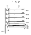
- Fig. 24 is a diagram showing characteristic elements of the ferroelectric memory according to the third embodiment, and showing address decoders 241, 242, a memory cell block 58, and a guarantee block 59 in a bank of the ferroelectric memory.
- the memory cell block 58 is constituted of first to fourth memory cell blocks BLK1 to BLK4 which are partitioned according to addresses for selecting a row direction (word line MWL).
- the guarantee block 59 is constituted of first to fourth guarantee blocks SC1 to SC4 which respectively correspond to the first to fourth blocks BLK1 to BLK4, and each of four guarantee cells connected to one bit line is arranged in each of the first to fourth guarantee blocks SC1 to SC4.
- the memory cell block 58 and the guarantee block 59 are each constituted of four blocks in Fig. 24, the number of blocks is not limited to four, which may be any number.
- the ferroelectric memory having the column units 56 constituted by the 2T/2C type memory cells is described as an example, but the present invention is applicable to a ferroelectric memory having column units constituted by the 1T/1C type memory cells.
- a guarantee cell having ferroelectric capacitors is connected, and by a read operation of data from a memory cell, data is read out from the memory cell, and the data is written to the guarantee cell. Accordingly, the data read out from the memory cell is automatically written to the guarantee cell, and the data can be retained securely until a restore operation completes, which make it possible to suppress loss of data due to destructive reading, and the data can be retained in a stable state even when the operation of the semiconductor memory device becomes incomplete or stops due to a power cut-off or the like. Therefore, regardless of operating condition of the semiconductor memory device, data can be securely retained as nonvolatile binary data, and the loss of data can be suppressed.
- the data can be restored by writing data retained in the guarantee cell to the memory cell after the power is turned on, which can suppress mismatch of data before and after the power cut-off.
Landscapes
- Engineering & Computer Science (AREA)
- Computer Hardware Design (AREA)
- Dram (AREA)
- Semiconductor Memories (AREA)
Abstract
Description
Claims (25)
- A semiconductor memory device, comprising:wherein during a read operation of data in connection with said memory cell, data is read out from said memory cell, and the data is written to said guarantee cell.a plurality of word lines;a plurality of plate lines provided adjacent to said word lines respectively;a plurality of bit lines provided in an orthogonal direction to said word lines and said plate lines;a memory cell provided at each intersection of pairs of said word lines and said plate lines adjacent to said word lines and said bit lines, said memory cell having a ferroelectric capacitor; anda guarantee cell connected commonly with said memory cell to said bit lines, said guarantee cell having a ferroelectric capacitor,
- The semiconductor memory device according to claim 1,
wherein data is written to said guarantee cell using potentials of said bit lines generated according to the data read from said memory cell. - The semiconductor memory device according to claim 1,
wherein said guarantee cell has the same cell structure as said memory cell. - The semiconductor memory device according to claim 1,
wherein said guarantee cell is constituted of a ferroelectric capacitor only. - The semiconductor memory device according to claim 1, further comprising:a guarantee flag cell storing a guarantee flag which indicates whether access processing to said memory cell is completed or not.
- The semiconductor memory device according to claim 5,
wherein said guarantee flag cell is connected to said plate line to which said guarantee cell is connected. - The semiconductor memory device according to claim 5,
wherein when power is turned on, it is judged whether the access processing is in a completed state or not based on the guarantee flag, and when the access processing is not in a completed state, data retained in said guarantee cell is written to said memory cell. - The semiconductor memory device according to claim 1,
wherein address information for accessing said memory cell is stored in a nonvolatile storage area. - The semiconductor memory device according to claim 8,
wherein the address information is stored in a guarantee cell which is included in a block in an inactive state provided in the same bank as a block which is activated based on the address information. - The semiconductor memory device according to claim 8, further comprising:a ferroelectric latch circuit having a ferroelectric capacitor retaining the address information.
- The semiconductor memory device according to claim 1, further comprising:a transfer gate controlling whether or not to electrically connect said bit line to which said memory cell is connected and said bit line to which said guarantee cell is connected.
- The semiconductor memory device according to claim 11, further comprising:a first precharge circuit connected to said bit line to which said memory cell is connected and configured to turn said bit line to a ground potential; anda second precharge circuit connected to said bit line to which said guarantee cell is connected and configured to turn said bit line to the ground potential.
- The semiconductor memory device according to claim 11,
wherein whether to enable a data guarantee function or not is optionally selectable, and when the data guarantee function is not enabled, said transfer gate is closed. - The semiconductor memory device according to claim 13, further comprising:a pad portion to which a signal line is connected, the signal line being associated with a control signal for optionally switching whether to enable the data guarantee function or not.
- The semiconductor memory device according to claim 13, further comprising:an external terminal to which a signal line is connected, the signal line being associated with a control signal for optionally switching whether to enable the data guarantee function or not.
- The semiconductor memory device according to claim 1, further comprising:a transfer gate controlling whether or not to electrically connect said guarantee cell to said bit line to which said memory cell is connected.
- The semiconductor memory device according to claim 1,
wherein a plurality of said guarantee cells are connected to said bit lines, and
wherein a guarantee cell to be used is selected from the plurality of said guarantee cells according to inputted address information. - The semiconductor memory device according to claim 1,
wherein an initial state of said guarantee cell is a state of having a polarization direction which is retained during a reading operation of data. - The semiconductor memory device according to claim 1,
wherein when reading or writing of data from/to said memory cell is performed, a potential of said plate line to which said guarantee cell is connected is a ground potential. - The semiconductor memory device according to claim 19,
wherein said guarantee cell is initialized by setting a potential of said connected plate line to a power supply potential. - The semiconductor memory device according to claim 1,
wherein during a precharge period to turn said bit line to a ground potential, said guarantee cell is initialized. - The semiconductor memory device according to claim 1,
wherein an address area of an address assigned to said memory cell and an address area of an address assigned to said guarantee cell are different. - The semiconductor memory device according to claim 1,
wherein said guarantee cell is provided in an address area to which access from the outside is prohibited. - The semiconductor memory device according to claim 11,
wherein when data is read out from said memory cell and thereafter data is written from the outside to said memory cell, said transfer gate is closed before the data from the outside is supplied to said bit line to which said memory cell is connected. - The semiconductor memory device according to claim 1,
wherein during a self check operation after power is turned on, access from the outside to said memory cell is prohibited, and a notification signal notifying that the self check operation is in progress is outputted to the outside.
Applications Claiming Priority (1)
| Application Number | Priority Date | Filing Date | Title |
|---|---|---|---|
| PCT/JP2003/003317 WO2004084227A1 (en) | 2003-03-19 | 2003-03-19 | Semiconductor memory |
Publications (3)
| Publication Number | Publication Date |
|---|---|
| EP1605468A1 true EP1605468A1 (en) | 2005-12-14 |
| EP1605468A4 EP1605468A4 (en) | 2006-08-02 |
| EP1605468B1 EP1605468B1 (en) | 2008-08-06 |
Family
ID=33018153
Family Applications (1)
| Application Number | Title | Priority Date | Filing Date |
|---|---|---|---|
| EP03715371A Expired - Lifetime EP1605468B1 (en) | 2003-03-19 | 2003-03-19 | Semiconductor memory |
Country Status (5)
| Country | Link |
|---|---|
| US (1) | US7133306B2 (en) |
| EP (1) | EP1605468B1 (en) |
| JP (1) | JP4125724B2 (en) |
| CN (1) | CN100446118C (en) |
| WO (1) | WO2004084227A1 (en) |
Families Citing this family (12)
| Publication number | Priority date | Publication date | Assignee | Title |
|---|---|---|---|---|
| FR2890483A1 (en) * | 2005-09-08 | 2007-03-09 | St Microelectronics Sa | REMAINING VOLATILE MEMORY CELL |
| WO2009025346A1 (en) * | 2007-08-22 | 2009-02-26 | Rohm Co., Ltd. | Data holding device |
| JP6015531B2 (en) * | 2013-04-01 | 2016-10-26 | 富士通セミコンダクター株式会社 | Logic circuit |
| US10373665B2 (en) | 2016-03-10 | 2019-08-06 | Micron Technology, Inc. | Parallel access techniques within memory sections through section independence |
| US9899073B2 (en) | 2016-06-27 | 2018-02-20 | Micron Technology, Inc. | Multi-level storage in ferroelectric memory |
| JP6625942B2 (en) * | 2016-07-29 | 2019-12-25 | 株式会社東芝 | Semiconductor storage device |
| US9812204B1 (en) * | 2016-10-28 | 2017-11-07 | AUCMOS Technologies USA, Inc. | Ferroelectric memory cell without a plate line |
| JP6860411B2 (en) * | 2017-04-27 | 2021-04-14 | ラピスセミコンダクタ株式会社 | Non-volatile semiconductor storage device |
| US11462249B2 (en) | 2020-06-30 | 2022-10-04 | Micron Technology, Inc. | System and method for reading and writing memory management data using a non-volatile cell based register |
| US11501815B2 (en) * | 2021-02-09 | 2022-11-15 | Micron Technology, Inc. | Sensing scheme for a memory with shared sense components |
| US11508426B1 (en) * | 2021-10-26 | 2022-11-22 | Ferroelectric Memory Gmbh | Memory device, memory cell arrangement, and methods thereof |
| CN116206642B (en) * | 2022-11-03 | 2024-03-29 | 北京超弦存储器研究院 | Semiconductor memory device having a memory cell with a memory cell having a memory cell with a memory cell |
Family Cites Families (13)
| Publication number | Priority date | Publication date | Assignee | Title |
|---|---|---|---|---|
| JP2823176B2 (en) | 1991-09-30 | 1998-11-11 | シャープ株式会社 | Nonvolatile storage device and readout method thereof |
| JP3590115B2 (en) * | 1994-12-20 | 2004-11-17 | 株式会社日立製作所 | Semiconductor memory |
| JPH098247A (en) * | 1995-06-15 | 1997-01-10 | Hitachi Ltd | Semiconductor memory device |
| JPH0997496A (en) * | 1995-09-29 | 1997-04-08 | Nec Corp | Ferroelectric substance memory device and data reading method |
| CN1183166A (en) * | 1996-03-25 | 1998-05-27 | 松下电子工业株式会社 | Ferroelectric memory device |
| JP3741230B2 (en) * | 1996-04-18 | 2006-02-01 | 株式会社日立製作所 | Ferroelectric memory |
| US5880989A (en) * | 1997-11-14 | 1999-03-09 | Ramtron International Corporation | Sensing methodology for a 1T/1C ferroelectric memory |
| JP2000187989A (en) * | 1998-12-24 | 2000-07-04 | Matsushita Electric Ind Co Ltd | Data storage device |
| DE10008243B4 (en) * | 2000-02-23 | 2005-09-22 | Infineon Technologies Ag | Integrated memory with plate line segments |
| JP4031904B2 (en) * | 2000-10-31 | 2008-01-09 | 富士通株式会社 | DATA READING CIRCUIT, DATA READING METHOD, AND DATA STORAGE DEVICE |
| JP4329919B2 (en) * | 2001-03-13 | 2009-09-09 | Okiセミコンダクタ株式会社 | Semiconductor memory and driving method of semiconductor memory |
| JP4146680B2 (en) * | 2002-07-18 | 2008-09-10 | 松下電器産業株式会社 | Ferroelectric memory device and reading method thereof |
| CN1303692C (en) * | 2002-09-04 | 2007-03-07 | 松下电器产业株式会社 | Semiconductor memory device, method for fabricating the same, and method for driving the same |
-
2003
- 2003-03-19 JP JP2004569574A patent/JP4125724B2/en not_active Expired - Fee Related
- 2003-03-19 WO PCT/JP2003/003317 patent/WO2004084227A1/en not_active Ceased
- 2003-03-19 CN CNB038245965A patent/CN100446118C/en not_active Expired - Fee Related
- 2003-03-19 EP EP03715371A patent/EP1605468B1/en not_active Expired - Lifetime
-
2005
- 2005-03-15 US US11/079,314 patent/US7133306B2/en not_active Expired - Lifetime
Also Published As
| Publication number | Publication date |
|---|---|
| US20050180222A1 (en) | 2005-08-18 |
| EP1605468A4 (en) | 2006-08-02 |
| CN1689110A (en) | 2005-10-26 |
| CN100446118C (en) | 2008-12-24 |
| WO2004084227A1 (en) | 2004-09-30 |
| JPWO2004084227A1 (en) | 2006-06-29 |
| US7133306B2 (en) | 2006-11-07 |
| JP4125724B2 (en) | 2008-07-30 |
| EP1605468B1 (en) | 2008-08-06 |
Similar Documents
| Publication | Publication Date | Title |
|---|---|---|
| US6317355B1 (en) | Nonvolatile ferroelectric memory device with column redundancy circuit and method for relieving failed address thereof | |
| US6950368B2 (en) | Low-voltage sense amplifier and method | |
| US6819582B2 (en) | Nonvolatile ferroelectric memory device with split word lines | |
| JP5196449B2 (en) | Semiconductor memory and program | |
| WO2006083034A1 (en) | Semiconductor storage apparatus and method for driving the same | |
| JPH08203266A (en) | Ferroelectric memory device | |
| EP1605468B1 (en) | Semiconductor memory | |
| KR0164377B1 (en) | Sub-word line driver | |
| JPH09134592A (en) | Sub-word line decoder of semiconductor memory device and semiconductor memory device thereof | |
| KR20130018588A (en) | Non-volatile static random access memory devices and methods of operations | |
| JP4357249B2 (en) | Semiconductor memory device | |
| US5698876A (en) | Memory standard cell macro for semiconductor device | |
| JP2004199726A (en) | Semiconductor storage device | |
| US6778422B2 (en) | Ferroelectric memory | |
| EP1598829A1 (en) | Semiconductor memory | |
| US7050323B2 (en) | Ferroelectric memory | |
| US7924605B2 (en) | Semiconductor memory device | |
| JP4477629B2 (en) | Ferroelectric memory | |
| KR100295301B1 (en) | Semiconductor mamory device with input/output masking function without destruction of data bit | |
| JP2004095135A (en) | Ferroelectric memory device and its program method | |
| JPH06309869A (en) | Semiconductor storage device | |
| JP2002352581A (en) | Semiconductor integrated circuit | |
| US7142465B2 (en) | Semiconductor memory | |
| KR20050113303A (en) | Sub word line driver in semiconductor memory device | |
| KR100334868B1 (en) | A high voltage generation device controlled by a refresh command |
Legal Events
| Date | Code | Title | Description |
|---|---|---|---|
| PUAI | Public reference made under article 153(3) epc to a published international application that has entered the european phase |
Free format text: ORIGINAL CODE: 0009012 |
|
| 17P | Request for examination filed |
Effective date: 20050331 |
|
| AK | Designated contracting states |
Kind code of ref document: A1 Designated state(s): AT BE BG CH CY CZ DE DK EE ES FI FR GB GR HU IE IT LI LU MC NL PT RO SE SI SK TR |
|
| RBV | Designated contracting states (corrected) |
Designated state(s): FR IT |
|
| A4 | Supplementary search report drawn up and despatched |
Effective date: 20060630 |
|
| REG | Reference to a national code |
Ref country code: DE Ref legal event code: 8566 |
|
| 17Q | First examination report despatched |
Effective date: 20061011 |
|
| GRAP | Despatch of communication of intention to grant a patent |
Free format text: ORIGINAL CODE: EPIDOSNIGR1 |
|
| GRAS | Grant fee paid |
Free format text: ORIGINAL CODE: EPIDOSNIGR3 |
|
| GRAA | (expected) grant |
Free format text: ORIGINAL CODE: 0009210 |
|
| AK | Designated contracting states |
Kind code of ref document: B1 Designated state(s): FR IT |
|
| REG | Reference to a national code |
Ref country code: FR Ref legal event code: TP |
|
| PLBE | No opposition filed within time limit |
Free format text: ORIGINAL CODE: 0009261 |
|
| STAA | Information on the status of an ep patent application or granted ep patent |
Free format text: STATUS: NO OPPOSITION FILED WITHIN TIME LIMIT |
|
| 26N | No opposition filed |
Effective date: 20090507 |
|
| PG25 | Lapsed in a contracting state [announced via postgrant information from national office to epo] |
Ref country code: IT Free format text: LAPSE BECAUSE OF FAILURE TO SUBMIT A TRANSLATION OF THE DESCRIPTION OR TO PAY THE FEE WITHIN THE PRESCRIBED TIME-LIMIT Effective date: 20080806 |
|
| PGFP | Annual fee paid to national office [announced via postgrant information from national office to epo] |
Ref country code: FR Payment date: 20090320 Year of fee payment: 7 |
|
| REG | Reference to a national code |
Ref country code: FR Ref legal event code: ST Effective date: 20101130 |
|
| PG25 | Lapsed in a contracting state [announced via postgrant information from national office to epo] |
Ref country code: FR Free format text: LAPSE BECAUSE OF NON-PAYMENT OF DUE FEES Effective date: 20100331 |