EP1604757A2 - Manufacturing method of die for optical element molding - Google Patents
Manufacturing method of die for optical element molding Download PDFInfo
- Publication number
- EP1604757A2 EP1604757A2 EP05251886A EP05251886A EP1604757A2 EP 1604757 A2 EP1604757 A2 EP 1604757A2 EP 05251886 A EP05251886 A EP 05251886A EP 05251886 A EP05251886 A EP 05251886A EP 1604757 A2 EP1604757 A2 EP 1604757A2
- Authority
- EP
- European Patent Office
- Prior art keywords
- manufacturing
- film layer
- die
- amorphous alloy
- super
- Prior art date
- Legal status (The legal status is an assumption and is not a legal conclusion. Google has not performed a legal analysis and makes no representation as to the accuracy of the status listed.)
- Granted
Links
- 230000003287 optical effect Effects 0.000 title claims abstract description 340
- 238000000465 moulding Methods 0.000 title claims abstract description 197
- 238000004519 manufacturing process Methods 0.000 title claims abstract description 122
- 229910000808 amorphous metal alloy Inorganic materials 0.000 claims abstract description 189
- 238000004781 supercooling Methods 0.000 claims abstract description 133
- 238000012546 transfer Methods 0.000 claims abstract description 132
- 239000000110 cooling liquid Substances 0.000 claims abstract description 129
- 239000012071 phase Substances 0.000 claims abstract description 128
- 239000000463 material Substances 0.000 claims abstract description 103
- 238000010438 heat treatment Methods 0.000 claims abstract description 34
- 230000009477 glass transition Effects 0.000 claims abstract description 24
- 239000000203 mixture Substances 0.000 claims description 74
- 238000000034 method Methods 0.000 claims description 62
- 229910052759 nickel Inorganic materials 0.000 claims description 32
- 229910052710 silicon Inorganic materials 0.000 claims description 26
- 229910052742 iron Inorganic materials 0.000 claims description 24
- 229910052726 zirconium Inorganic materials 0.000 claims description 24
- 229910052763 palladium Inorganic materials 0.000 claims description 23
- 229910052799 carbon Inorganic materials 0.000 claims description 22
- 229910052718 tin Inorganic materials 0.000 claims description 22
- 229910052782 aluminium Inorganic materials 0.000 claims description 21
- 229910052802 copper Inorganic materials 0.000 claims description 21
- 229910052796 boron Inorganic materials 0.000 claims description 20
- 229910003460 diamond Inorganic materials 0.000 claims description 20
- 239000010432 diamond Substances 0.000 claims description 20
- 229910052698 phosphorus Inorganic materials 0.000 claims description 20
- 239000010970 precious metal Substances 0.000 claims description 20
- 229910052719 titanium Inorganic materials 0.000 claims description 20
- OKTJSMMVPCPJKN-UHFFFAOYSA-N Carbon Chemical compound [C] OKTJSMMVPCPJKN-UHFFFAOYSA-N 0.000 claims description 17
- 229910052751 metal Inorganic materials 0.000 claims description 17
- MCMNRKCIXSYSNV-UHFFFAOYSA-N Zirconium dioxide Chemical compound O=[Zr]=O MCMNRKCIXSYSNV-UHFFFAOYSA-N 0.000 claims description 16
- 229910052735 hafnium Inorganic materials 0.000 claims description 14
- 230000000694 effects Effects 0.000 claims description 13
- 229910052721 tungsten Inorganic materials 0.000 claims description 12
- 230000008859 change Effects 0.000 claims description 11
- 230000004075 alteration Effects 0.000 claims description 10
- 238000005229 chemical vapour deposition Methods 0.000 claims description 10
- 229910052741 iridium Inorganic materials 0.000 claims description 10
- 238000005240 physical vapour deposition Methods 0.000 claims description 10
- 239000002994 raw material Substances 0.000 claims description 10
- 229910052703 rhodium Inorganic materials 0.000 claims description 10
- 229910052709 silver Inorganic materials 0.000 claims description 10
- 229910052750 molybdenum Inorganic materials 0.000 claims description 9
- ATJFFYVFTNAWJD-UHFFFAOYSA-N Tin Chemical compound [Sn] ATJFFYVFTNAWJD-UHFFFAOYSA-N 0.000 claims description 8
- PNEYBMLMFCGWSK-UHFFFAOYSA-N aluminium oxide Inorganic materials [O-2].[O-2].[O-2].[Al+3].[Al+3] PNEYBMLMFCGWSK-UHFFFAOYSA-N 0.000 claims description 8
- 229910052804 chromium Inorganic materials 0.000 claims description 8
- 229910052697 platinum Inorganic materials 0.000 claims description 8
- 239000000126 substance Substances 0.000 claims description 8
- 229910052723 transition metal Inorganic materials 0.000 claims description 8
- 229910010037 TiAlN Inorganic materials 0.000 claims description 7
- 230000002265 prevention Effects 0.000 claims description 7
- 238000001771 vacuum deposition Methods 0.000 claims description 7
- 238000007733 ion plating Methods 0.000 claims description 5
- 230000008602 contraction Effects 0.000 claims description 3
- 229910052707 ruthenium Inorganic materials 0.000 claims description 3
- 229910052737 gold Inorganic materials 0.000 claims description 2
- 238000007740 vapor deposition Methods 0.000 claims description 2
- 229910052727 yttrium Inorganic materials 0.000 claims description 2
- 229910052581 Si3N4 Inorganic materials 0.000 claims 4
- JMANVNJQNLATNU-UHFFFAOYSA-N oxalonitrile Chemical compound N#CC#N JMANVNJQNLATNU-UHFFFAOYSA-N 0.000 claims 4
- HQVNEWCFYHHQES-UHFFFAOYSA-N silicon nitride Chemical compound N12[Si]34N5[Si]62N3[Si]51N64 HQVNEWCFYHHQES-UHFFFAOYSA-N 0.000 claims 4
- UONOETXJSWQNOL-UHFFFAOYSA-N tungsten carbide Chemical compound [W+]#[C-] UONOETXJSWQNOL-UHFFFAOYSA-N 0.000 claims 4
- -1 TiA1N Chemical compound 0.000 claims 2
- 239000010410 layer Substances 0.000 description 122
- 238000012545 processing Methods 0.000 description 48
- 230000008569 process Effects 0.000 description 34
- KDLHZDBZIXYQEI-UHFFFAOYSA-N palladium Substances [Pd] KDLHZDBZIXYQEI-UHFFFAOYSA-N 0.000 description 33
- PXHVJJICTQNCMI-UHFFFAOYSA-N Nickel Chemical compound [Ni] PXHVJJICTQNCMI-UHFFFAOYSA-N 0.000 description 30
- 238000005520 cutting process Methods 0.000 description 30
- XEEYBQQBJWHFJM-UHFFFAOYSA-N iron Substances [Fe] XEEYBQQBJWHFJM-UHFFFAOYSA-N 0.000 description 20
- 239000000956 alloy Substances 0.000 description 16
- 229910045601 alloy Inorganic materials 0.000 description 14
- 230000015572 biosynthetic process Effects 0.000 description 13
- 238000007747 plating Methods 0.000 description 11
- 230000003578 releasing effect Effects 0.000 description 11
- 239000013590 bulk material Substances 0.000 description 9
- 238000001816 cooling Methods 0.000 description 9
- 238000002425 crystallisation Methods 0.000 description 8
- 230000008025 crystallization Effects 0.000 description 8
- 239000011521 glass Substances 0.000 description 8
- 238000000227 grinding Methods 0.000 description 8
- 239000002184 metal Substances 0.000 description 8
- 239000004033 plastic Substances 0.000 description 7
- 230000001681 protective effect Effects 0.000 description 7
- 239000013078 crystal Substances 0.000 description 6
- 239000005300 metallic glass Substances 0.000 description 6
- 238000005516 engineering process Methods 0.000 description 5
- 230000002093 peripheral effect Effects 0.000 description 5
- 239000010703 silicon Substances 0.000 description 5
- 230000000052 comparative effect Effects 0.000 description 4
- 238000012937 correction Methods 0.000 description 4
- 230000004907 flux Effects 0.000 description 4
- 239000002245 particle Substances 0.000 description 4
- 230000009471 action Effects 0.000 description 3
- 230000003247 decreasing effect Effects 0.000 description 3
- 230000006866 deterioration Effects 0.000 description 3
- 239000006185 dispersion Substances 0.000 description 3
- 238000003825 pressing Methods 0.000 description 3
- 239000010935 stainless steel Substances 0.000 description 3
- 229910001220 stainless steel Inorganic materials 0.000 description 3
- 229910000831 Steel Inorganic materials 0.000 description 2
- 239000012530 fluid Substances 0.000 description 2
- 239000007789 gas Substances 0.000 description 2
- 150000002739 metals Chemical class 0.000 description 2
- 238000004554 molding of glass Methods 0.000 description 2
- 230000003647 oxidation Effects 0.000 description 2
- 238000007254 oxidation reaction Methods 0.000 description 2
- 239000011241 protective layer Substances 0.000 description 2
- 239000010959 steel Substances 0.000 description 2
- 238000003860 storage Methods 0.000 description 2
- 239000013077 target material Substances 0.000 description 2
- 230000007704 transition Effects 0.000 description 2
- UFHFLCQGNIYNRP-UHFFFAOYSA-N Hydrogen Chemical compound [H][H] UFHFLCQGNIYNRP-UHFFFAOYSA-N 0.000 description 1
- 230000005540 biological transmission Effects 0.000 description 1
- 229910052794 bromium Inorganic materials 0.000 description 1
- 239000000919 ceramic Substances 0.000 description 1
- 238000004891 communication Methods 0.000 description 1
- 239000000498 cooling water Substances 0.000 description 1
- 230000007547 defect Effects 0.000 description 1
- 238000011161 development Methods 0.000 description 1
- 238000001312 dry etching Methods 0.000 description 1
- 238000007772 electroless plating Methods 0.000 description 1
- 230000007613 environmental effect Effects 0.000 description 1
- BHEPBYXIRTUNPN-UHFFFAOYSA-N hydridophosphorus(.) (triplet) Chemical compound [PH] BHEPBYXIRTUNPN-UHFFFAOYSA-N 0.000 description 1
- 229910052739 hydrogen Inorganic materials 0.000 description 1
- 239000001257 hydrogen Substances 0.000 description 1
- 238000001746 injection moulding Methods 0.000 description 1
- 238000003754 machining Methods 0.000 description 1
- 235000012054 meals Nutrition 0.000 description 1
- 238000005272 metallurgy Methods 0.000 description 1
- 238000010137 moulding (plastic) Methods 0.000 description 1
- 150000004767 nitrides Chemical class 0.000 description 1
- 230000010355 oscillation Effects 0.000 description 1
- 150000002940 palladium Chemical class 0.000 description 1
- 239000010453 quartz Substances 0.000 description 1
- 230000009467 reduction Effects 0.000 description 1
- 239000011347 resin Substances 0.000 description 1
- 229920005989 resin Polymers 0.000 description 1
- SBIBMFFZSBJNJF-UHFFFAOYSA-N selenium;zinc Chemical compound [Se]=[Zn] SBIBMFFZSBJNJF-UHFFFAOYSA-N 0.000 description 1
- 238000007086 side reaction Methods 0.000 description 1
- VYPSYNLAJGMNEJ-UHFFFAOYSA-N silicon dioxide Inorganic materials O=[Si]=O VYPSYNLAJGMNEJ-UHFFFAOYSA-N 0.000 description 1
- 239000000243 solution Substances 0.000 description 1
- 239000004575 stone Substances 0.000 description 1
- 239000000758 substrate Substances 0.000 description 1
- 230000003746 surface roughness Effects 0.000 description 1
- 238000001721 transfer moulding Methods 0.000 description 1
- 238000007738 vacuum evaporation Methods 0.000 description 1
- XLYOFNOQVPJJNP-UHFFFAOYSA-N water Substances O XLYOFNOQVPJJNP-UHFFFAOYSA-N 0.000 description 1
Images
Classifications
-
- B—PERFORMING OPERATIONS; TRANSPORTING
- B29—WORKING OF PLASTICS; WORKING OF SUBSTANCES IN A PLASTIC STATE IN GENERAL
- B29C—SHAPING OR JOINING OF PLASTICS; SHAPING OF MATERIAL IN A PLASTIC STATE, NOT OTHERWISE PROVIDED FOR; AFTER-TREATMENT OF THE SHAPED PRODUCTS, e.g. REPAIRING
- B29C33/00—Moulds or cores; Details thereof or accessories therefor
- B29C33/42—Moulds or cores; Details thereof or accessories therefor characterised by the shape of the moulding surface, e.g. ribs or grooves
- B29C33/424—Moulding surfaces provided with means for marking or patterning
-
- C—CHEMISTRY; METALLURGY
- C12—BIOCHEMISTRY; BEER; SPIRITS; WINE; VINEGAR; MICROBIOLOGY; ENZYMOLOGY; MUTATION OR GENETIC ENGINEERING
- C12G—WINE; PREPARATION THEREOF; ALCOHOLIC BEVERAGES; PREPARATION OF ALCOHOLIC BEVERAGES NOT PROVIDED FOR IN SUBCLASSES C12C OR C12H
- C12G3/00—Preparation of other alcoholic beverages
- C12G3/08—Preparation of other alcoholic beverages by methods for altering the composition of fermented solutions or alcoholic beverages not provided for in groups C12G3/02 - C12G3/07
-
- C—CHEMISTRY; METALLURGY
- C03—GLASS; MINERAL OR SLAG WOOL
- C03B—MANUFACTURE, SHAPING, OR SUPPLEMENTARY PROCESSES
- C03B11/00—Pressing molten glass or performed glass reheated to equivalent low viscosity without blowing
- C03B11/06—Construction of plunger or mould
- C03B11/08—Construction of plunger or mould for making solid articles, e.g. lenses
- C03B11/082—Construction of plunger or mould for making solid articles, e.g. lenses having profiled, patterned or microstructured surfaces
-
- C—CHEMISTRY; METALLURGY
- C03—GLASS; MINERAL OR SLAG WOOL
- C03B—MANUFACTURE, SHAPING, OR SUPPLEMENTARY PROCESSES
- C03B11/00—Pressing molten glass or performed glass reheated to equivalent low viscosity without blowing
- C03B11/06—Construction of plunger or mould
- C03B11/08—Construction of plunger or mould for making solid articles, e.g. lenses
- C03B11/084—Construction of plunger or mould for making solid articles, e.g. lenses material composition or material properties of press dies therefor
- C03B11/086—Construction of plunger or mould for making solid articles, e.g. lenses material composition or material properties of press dies therefor of coated dies
-
- C—CHEMISTRY; METALLURGY
- C03—GLASS; MINERAL OR SLAG WOOL
- C03B—MANUFACTURE, SHAPING, OR SUPPLEMENTARY PROCESSES
- C03B2215/00—Press-moulding glass
- C03B2215/02—Press-mould materials
- C03B2215/08—Coated press-mould dies
- C03B2215/14—Die top coat materials, e.g. materials for the glass-contacting layers
- C03B2215/16—Metals or alloys, e.g. Ni-P, Ni-B, amorphous metals
-
- C—CHEMISTRY; METALLURGY
- C03—GLASS; MINERAL OR SLAG WOOL
- C03B—MANUFACTURE, SHAPING, OR SUPPLEMENTARY PROCESSES
- C03B2215/00—Press-moulding glass
- C03B2215/02—Press-mould materials
- C03B2215/08—Coated press-mould dies
- C03B2215/14—Die top coat materials, e.g. materials for the glass-contacting layers
- C03B2215/16—Metals or alloys, e.g. Ni-P, Ni-B, amorphous metals
- C03B2215/17—Metals or alloys, e.g. Ni-P, Ni-B, amorphous metals comprising one or more of the noble meals, i.e. Ag, Au, platinum group metals
-
- C—CHEMISTRY; METALLURGY
- C03—GLASS; MINERAL OR SLAG WOOL
- C03B—MANUFACTURE, SHAPING, OR SUPPLEMENTARY PROCESSES
- C03B2215/00—Press-moulding glass
- C03B2215/02—Press-mould materials
- C03B2215/08—Coated press-mould dies
- C03B2215/14—Die top coat materials, e.g. materials for the glass-contacting layers
- C03B2215/20—Oxide ceramics
-
- C—CHEMISTRY; METALLURGY
- C03—GLASS; MINERAL OR SLAG WOOL
- C03B—MANUFACTURE, SHAPING, OR SUPPLEMENTARY PROCESSES
- C03B2215/00—Press-moulding glass
- C03B2215/02—Press-mould materials
- C03B2215/08—Coated press-mould dies
- C03B2215/14—Die top coat materials, e.g. materials for the glass-contacting layers
- C03B2215/22—Non-oxide ceramics
-
- C—CHEMISTRY; METALLURGY
- C03—GLASS; MINERAL OR SLAG WOOL
- C03B—MANUFACTURE, SHAPING, OR SUPPLEMENTARY PROCESSES
- C03B2215/00—Press-moulding glass
- C03B2215/02—Press-mould materials
- C03B2215/08—Coated press-mould dies
- C03B2215/14—Die top coat materials, e.g. materials for the glass-contacting layers
- C03B2215/24—Carbon, e.g. diamond, graphite, amorphous carbon
-
- C—CHEMISTRY; METALLURGY
- C03—GLASS; MINERAL OR SLAG WOOL
- C03B—MANUFACTURE, SHAPING, OR SUPPLEMENTARY PROCESSES
- C03B2215/00—Press-moulding glass
- C03B2215/02—Press-mould materials
- C03B2215/08—Coated press-mould dies
- C03B2215/30—Intermediate layers, e.g. graded zone of base/top material
- C03B2215/32—Intermediate layers, e.g. graded zone of base/top material of metallic or silicon material
-
- C—CHEMISTRY; METALLURGY
- C03—GLASS; MINERAL OR SLAG WOOL
- C03B—MANUFACTURE, SHAPING, OR SUPPLEMENTARY PROCESSES
- C03B2215/00—Press-moulding glass
- C03B2215/02—Press-mould materials
- C03B2215/08—Coated press-mould dies
- C03B2215/30—Intermediate layers, e.g. graded zone of base/top material
- C03B2215/34—Intermediate layers, e.g. graded zone of base/top material of ceramic or cermet material, e.g. diamond-like carbon
-
- C—CHEMISTRY; METALLURGY
- C03—GLASS; MINERAL OR SLAG WOOL
- C03B—MANUFACTURE, SHAPING, OR SUPPLEMENTARY PROCESSES
- C03B2215/00—Press-moulding glass
- C03B2215/40—Product characteristics
- C03B2215/41—Profiled surfaces
- C03B2215/412—Profiled surfaces fine structured, e.g. fresnel lenses, prismatic reflectors, other sharp-edged surface profiles
-
- Y—GENERAL TAGGING OF NEW TECHNOLOGICAL DEVELOPMENTS; GENERAL TAGGING OF CROSS-SECTIONAL TECHNOLOGIES SPANNING OVER SEVERAL SECTIONS OF THE IPC; TECHNICAL SUBJECTS COVERED BY FORMER USPC CROSS-REFERENCE ART COLLECTIONS [XRACs] AND DIGESTS
- Y02—TECHNOLOGIES OR APPLICATIONS FOR MITIGATION OR ADAPTATION AGAINST CLIMATE CHANGE
- Y02P—CLIMATE CHANGE MITIGATION TECHNOLOGIES IN THE PRODUCTION OR PROCESSING OF GOODS
- Y02P40/00—Technologies relating to the processing of minerals
- Y02P40/50—Glass production, e.g. reusing waste heat during processing or shaping
- Y02P40/57—Improving the yield, e-g- reduction of reject rates
Definitions
- the present invention relates to a manufacturing method for manufacturing a die for optical element molding by using a master die.
- a blank (primary product) is manufactured by, for example, steel or stainless steel, and an alloy of an amorphous-like nickel and phosphorous is filmed in the thickness of about 100 ⁇ m by a chemical plating, which is called electroless plating, on it, and this plating layer is cutting processed by a diamond tool in an ultra-precise processing machine, and a highly accurate optical surface transfer surface for molding the optical surface of the optical element is obtained.
- the optical surface transfer surface is largely cutting processed by a diamond tool, however, in such a case, the influence such as a condition of a cutting edge of the tool or processing condition, a change of processing environmental temperature is exerted, and there is also a problem that the shape of the optical surface transfer surface finished after cutting processing, is delicately dispersed.
- This processing dispersion of the optical surface transfer surface is due to the poorness of the machinability of the raw material.
- the optical surface shape error of about 100 nm is generated, and even in the case where processing is conducted very carefully, the shape error of about 50 nm is remained. This is a limit of processing accuracy when a large amount of optical surface transfer surfaces of the same shape are created.
- an optical element in which a ring-shaped zone diffraction groove (diffraction ring-shaped zone) is provided on the optical surface and by which the chromatic aberration is efficiently corrected is put into practical use in the optical information recording field, and a large amount of optical elements are manufactured.
- an optical material plastic or glass is used, however, in the infrared optical system, a crystal material such as ZnSe is also used.
- Such an optical element can be produced in a large amount and effectively by molding, however, it is a very important problem, at the time of molding, how high-accurately and effectively minute diffraction grooves on the optical surface of the optical element are manufactured by the die for optical element molding.
- the sharpness of the cutting edge controls the exactness of the diffraction groove shape, and when it is transferred as the optical surface of the optical element, the diffraction efficiency is largely influenced.
- the dimension of the cutting edge is made sufficiently small, in such a case, because, on the small cutting edge portion, the cutting resistance is concentrically imposed, it is necessary that the incised amount is decreased, and the number of time of processing is increased until the entire optical surface is uniformly cut and removed. Further, it is necessary that the feed speed of the tool is made slow in order also to prevent the deterioration of the surface roughness of the optical surface by the cutter mark of the small cutting edge, and the optical surface transfer surface processing time of one time also becomes long.
- the minute structure which is several times smaller or less than the wavelength of the light source to be used, is provided on the optical surface and a new optical function is added to the optical element.
- the ordinary light converging function by the refraction of the molded lens and a positive dispersion generated as the side reaction at the time are cancelled by using a large negative dispersion by the diffraction obtained when the diffraction groove is provided on the surface of the aspheric surface optical surface, and a method in which the achromatic function, which is originally impossible only by the refraction, is added to a single lens optical element, is put in practice in the objective lens for pick-up apparatus for optical disk, which is DVD/CD compatible.
- the optical surface on which protrusions like this are formed is a minute structure which is so-called a moth eye, and when the structural bodies which are minuter than the wavelength of the light are arranged in a period shorter than the wavelength, any longer, each structure is not diffracted and acts on the light wave as an average refractive index.
- Such an area is generally called an equivalent refractive index area. Relating to such an equivalent refractive index area, for example, it is written in Institute of electronic information communication papers C Vol. J83-C No.3 pp. 173 - 181, March, 2000.
- the minute structure of the equivalent refractive index area According to the minute structure of the equivalent refractive index area, a larger reflection prevention effect can be obtained than the conventional reflection prevention coat while the angle dependency of the reflection prevention effect or wavelength dependency is deceased.
- plastic molding because the optical surface and the minute structure are simultaneously created, it is considered that a merit in the production in which the lens function and the reflection prevention function are simultaneously obtained, and the after processing that the reflection prevention coat processing is conducted after the molding is not necessary, is large, and is remarked.
- the strong optical anisotropy can be given to the optical surface.
- the double refraction optical element which is conventionally manufactured by cutting the crystal such as quartz crystal, can be obtained by molding. Further, when it is combined with a refraction or reflection optical element, a new optical function can be added to it.
- the optical anisotropy in this case is called a structural double refraction.
- the optical element when the optical element is formed by using the scalar area, equivalent refractive index area or resonance area, it is necessary to form the minute protrusions (or hollows)on the optical surface.
- the molding In order to make mass-production of the optical element having such minute protrusions (or hollows), generally, it can be said appropriate that the molding is conducted by making plastic as a raw material.
- the optical surface transfer surface provided with the hollows (or protrusions) corresponding to the minute protrusions (or hollows) is provided in the die for molding of the optical element.
- the minute structure is blaze-shape or sinking comb-shape
- it is difficult to push the metallic glass to the bottom of groove as the result, there is also a possibility that the tip of the minute structure corresponding to the blaze-shape or sinking comb-shape transferred on the molding transfer surface of the die for optical element molding is brought to a rounded shape.
- the optical element is molded by such a die for optical element molding, because its molding transfer surface shape is transferred onto the optical surface of the optical element as it is, the optical surface of the optical element in which the shape of the primary part of the blaze-shape or sinking comb-shape is inaccurate, is formed, and characteristic of the optical element is lowered.
- the present invention is attained in view of such a problem of conventional technology, and the object of the present invention is to provide a manufacturing method of the die for optical element molding which is easily manufactured and which can increase the dimension accuracy of the optical element.
- One of modes of the present invention is a manufacturing method of the die for optical element molding, and which is characterized in that it has: a process for forming the first film layer of the amorphous alloy having the super-cooling liquid phase formed of a predetermined composition on the master transfer surface of the master die for molding the molding transfer surface of the die for optical element molding; a process for heating the first film layer (called also a heating press process) more than the glass transition point of the amorphous alloy having the super-cooling liquid phase while pressing under the condition that the surface of the first film layer and the shifted surface of the base material of the die for optical element molding are faced; and a process for peeling the first film layer from the master die, and for shifting the first film layer to the base material of the die for optical element molding.
- the present invention is a method in which the film layer of the amorphous alloy having the super-cooling liquid phase is formed on the master transfer surface of the master die and by shifting this to the die for optical element molding, the molding transfer surface is obtained.
- the shape of the master transfer surface of the master die is transferred onto the transferred surface of the die, because the dynamic transfer by the heating press is not used, even in a case where a minute structure is formed on the master transfer surface, the possibility that it is broken is very low.
- the very accurate molding transfer surface (for example, the shape accuracy is less than 50 nm to the master die) can be obtained. Accordingly, when one master die having an accurate master transfer surface is created, any number of the die for optical element molding having the same molding transfer surface shape can be obtained.
- Patent Documents relating to a bulk material of the amorphous alloy having the super-cooling area are well known.
- the amorphous alloy metal having the super-cooling area of the bulk material there is a problem that it is difficult to stably manufacture the amorphous condition of the crystal structure which is a its large characteristic.
- the alloy (called mother alloy) is manufactured in the arc furnace in the way of desired composition, and the mother alloy is heated in the high temperature and liquefied, after that, rapidly cooled at the cooling speed of 10 4 °C/sec.
- the mother alloy is an alloy only mixed with the metal of the same composition ratio in the furnace, and the crystal condition is a polycrystalline substance. Accordingly, in order to obtain the amorphous alloy having the super-cooling liquid phase of the bulk material, because this cooling process is absolutely necessary, man-day is increased and the manufacturing method is limited because the heated alloy is uniformly rapidly cooled, and further, the skill is necessary for the cooling technology.
- the amorphous alloy having the super-cooling liquid phase can be piled in a form of film, and for example, when only a mother alloy can be prepared as a target, because the amorphous alloy having a thin film-like super-cooling liquid phase can be comparatively easily obtained, as compared to a case where the bulk material is used, the manufacturing time period is very much shortened. Further, because the film can be formed into the essential film thickness, the saving of the amorphous alloy having the super-cooling liquid phase can be intended, and the manufacturing cost can be suppressed.
- the amorphous condition is not always necessary, and when a desired composition ratio is satisfied, there is also a merit that, by scattering and piling particles, it is naturally brought into the amorphous condition. That is, when only a mother alloy target of the same composition ratio as the amorphous alloy having a desired super-cooling liquid phase is prepared, also for the amorphous alloy having the super-cooling liquid phase of the material ⁇ composition ratio in which it is difficult to be stably produced in the bulk material, further, also for the material ⁇ composition ratio which is not made into the amorphous in the bulk material, it can be easily made into the amorphous and the film can be formed.
- the amorphous alloy having the super-cooling liquid phase so-called metallic glass will be described.
- This is structured by amorphous alloy material which is brought into the super-cooling liquid when heated, and in contrast to that the ordinary metals are poly-crystal structure, because the structure is amorphous-like, the composition is uniform also in micro-structure, and this is excellent in the mechanical strength or normal temperature chemical resistance, and has the glass transition point, and because, when it is heated in the range between the glass transition point which is the super-cooling liquid phase and the crystallization temperature (normally, the glass transition point is +10 - +100 °C), it is softened into glass-like (becomes viscous fluid body), it has the characteristic which normal metals do not have, and in which the press molding processing can be conducted.
- the material which is conventionally known is only soft metal, and only by ductility-mode cutting by the amount of very minute depth of cut (about 100 nm), the high hardness material such as silicon or glass can be cutting-processed, however, the efficiency is very low. Accordingly, it can be said that, to use the amorphous alloy as the die material, is a discovery for suggesting the very large application development for the optical surface creation processing centering around the master die. The same processing characteristic comes oout in a form that the grinding ratio can be obtained largely, also for the grinding processing by using the diamond grinding stone.
- the film thickness of the amorphous alloy having the super-cooling liquid phase formed in the master die it is 0.01 ⁇ m - 500 ⁇ m. In the case of the film thickness within this range, the generation of pit is suppressed, and it can be uniformly heated when the amorphous alloy is shifted from the master die to the transferred surface of the metallic mold, and a possibility that the amorphous alloy is crystallized when one portion of it is excessively heated, is low. In the view point in the same manner, it is preferable that the film thickness is 10 - 200 ⁇ m, further, it is preferable that the film thickness is 10 - 100 ⁇ m.
- the manufacturing method of the die for optical element molding has a process for forming the second film layer of the amorphous alloy having the super-cooling liquid phase on a shifted surface of the base material of the die for optical element molding.
- the first film layer is shifted to the base material of the die for optical element molding
- composition of the amorphous alloy having the super-cooling liquid phase of the first film layer formed on the master transfer surface of the master die and the composition of the amorphous alloy having the super-cooling liquid phase of the second film layer formed on the transferred surface of the die for the optical element molding are the same.
- the film layer of the same composition as the film layer of the amorphous alloy having the super-cooling liquid phase formed on the master die is formed also on the base material of the die for the optical element molding, when the film layer of the amorphous alloy having the super-cooling liquid phase formed on the master die and the contact surface of the film layer of the amorphous alloy having the super-cooling liquid phase formed on the base material are heated and close contact with each other, the adhesion of mutual film layers is increased because they have the same composition.
- the adhesion of the base material to the amorphous alloy film layer can be more increased. Thereby, an increase of the durability (life) of the die for the optical element molding can be intended.
- the manufacturing method of the die for the optical element molding has a process for forming the second film layer of the amorphous alloy having the super-cooling liquid phase on the shifted surface of the base material of the die for the optical element molding before a process by which at least the first film layer is peeled from the master die and shifted to the base material of the die for the optical element molding
- the composition of the amorphous alloy having the super-cooling liquid phase of the first film layer and the composition of the amorphous alloy having the super-cooling liquid phase of the second film layer are different from each other.
- the film layer of the amorphous alloy having the super-cooling liquid phase formed on the base material of the die for the optical element molding is composed of the different composition from the film layer of the amorphous alloy having the super-cooling liquid phase formed on the master die, the glass transition points can be differed from each other.
- the temperature areas can be respectively changed when the film layer of the amorphous alloy having the super-cooling liquid phase is peeled from the master die.
- the film thickness of the second film layer formed on the transferred surface of the base material of the die for the optical element molding in the same as the first film layer formed on the master transfer surface of the master die, it is preferable that the film thickness is 0.01 ⁇ m - 500 ⁇ m. From the same reason, in the same view point, 10 - 200 ⁇ m is preferable, and further, 10 - 100 ⁇ m is preferable.
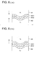
- Fig. 6(a) it is assumed that the film layer of the amorphous alloy MG1 having the super-cooling liquid phase is formed on the master die M1 and the film layer of the amorphous alloy MG2 having the super-cooling liquid phase is formed on the master die M2.
- the master die M1 and the die M2 for optical element molding are heated to the temperature T1 (350 °C ⁇ T1: where, T1 is not larger than the glass crystallization temperature) more than the glass transition point of the amorphous alloy of the formed film layer, and as shown in Fig. 6(a), the film layers of the amorphous alloy are faced so that they are brought into contact with each other, and pressed. After that, they are cooled once, and the die temperature is lowered from temperature T1.
- T1 350 °C ⁇ T1: where, T1 is not larger than the glass crystallization temperature
- the die temperature of only the master die M1 side is heated to T2 (300 °C ⁇ T2 ⁇ 350 °C: where, T2 is not larger than the glass crystallization temperature), and the die temperature of the die M2 side for optical element molding is made to keep the temperature T1' ( ⁇ 300 °C), the mutual bonding strength of the amorphous alloy MG1 and the master die M1 is weakened more than the mutual bonding power of the die M2 for optical element molding and the amorphous alloy MG2, and more than the mutual bonding power of the amorphous alloy MG2, MG1. From such a condition, as shown in Fig.
- the amorphous alloy MG1 when the master die M1 is separated from the die M2 for optical element molding, the amorphous alloy MG1 is peeled as its shape is transferred from the master die M1 and further, cooled to the normal temperature, it forms a part of the die M2 for optical element molding together with the amorphous alloy MG2. That is, when the glass transition point temperatures of the amorphous alloys MG1, MG2 are adjusted, the mold-releasing property can be increased.
- the die for optical element molding of the present invention it is preferable that it has a process by which the function film (the first function film) is provided on the master transfer surface, before a process by which the film layer of the amorphous alloy having the super-cooling liquid phase is formed on the master transfer surface of the master die.
- the first function film contains at least one kind of element selected from precious metal elements of Pt, Ir, Ru, Rh, Ag, transition metal elements of Fe, Co, Ni, Cr, W, Ti, Mo, Zr, and alumina, chromina, wc, nitriding-silicon, nitriding-carbon, TiN, TiAlN, zirconia, diamond, diamond-like carbon, carbon.
- the first function film contains at least one kind of element selected from the precious metal elements of Pt, Ir, Pd, Au, Ru, Rh, Ag, and the transition metal elements of Fe, Co, Ni, Cr, W, Ti, Mo, Zr.
- function films listed in them has a function as the protective film, for example, at the time of molding of glass mold, and in order to improve the mold-releasing function between the glass and the metallic mold at the time of molding, the function film is provided on the molding transfer surface of the metallic mold.
- the mold-releasing performance when the film layer of the amorphous alloy having the super-cooling liquid phase is peeled from the master die can be increased, and the breakage of the film layer at the time of peeling can be prevented.
- this function film layer can function as the protective layer of the metallic mold, and there is an effect that the film layer of the amorphous alloy having the super-cooling liquid phase or the material is protected from the influence such as the breakage ⁇ deterioration ⁇ adhesion from the heat or pressure at the time of the molding transfer of the optical element.
- the first function film also contains at least one material selected from materials of alumina, chromina, WC, nitriding-silicon, nitriding-carbon, TiN, TiAlN, zirconia, diamond, diamond-like carbon, carbon.
- function films listed in them has a function as the protective film, for example, at the time of molding of glass mold, and in order to improve the mold-releasing function between the glass and the metallic mold at the time of molding, the function film is provided on the molding transfer surface of the metallic mold.
- the mold-releasing performance when the film layer of the amorphous alloy having the super-cooling liquid phase is peeled from the master die can be increased, and the breakage of the film layer at the time of peeling can be prevented.
- this function film layer can function as the protective layer of the metallic mold, and there is an effect that the film layer of the amorphous alloy having the super-cooling liquid phase or the material is protected from the influence such as the breakage ⁇ deterioration ⁇ adhesion from the heat or pressure at the time of the molding transfer of the optical element.
- the film thickness of the first function film of the present invention is 0.01 - 20 ⁇ m.
- the function as the mold-releasing property or protective film can be obtained.
- the die for optical element molding of the present invention it is further preferable that it has a process by which the second function film is further provided on the film of the first function film before a process by which the film layer of the amorphous alloy having the super-cooling liquid phase is formed.
- the second function film also contains at least one kind of element selected from the precious metal elements of Pt, Ir, Pd, Au, Ru, Rh, Ag, transition metal elements of Fe, Co, Ni, Cr, W, Ti, Mo, Zr, and alumina, chromina, wc, nitriding-silicon, nitriding-carbon, TiN, TiAlN, zirconia, diamond, diamond-like carbon, carbon.
- the second function film contains at least one kind of element selected from the precious metal elements of Pt, Ir, Pd, Au, Ru, Rh, Ag, and the transition metal elements of Fe, Co, Ni, Cr, W, Ti, Mo, Zr.
- the second function film contains at least one kind of material selected from alumina, chromina, wc, nitriding-silicon, nitriding-carbon, TiN, TiAlN, zirconia, diamond, diamond-like carbon, carbon.
- the die-releasing effect from the master die at the time of molding transfer can be given, for example, to the first function film closest from the master transfer surface of the master die, and the effect as the die protective film can be given to the second function film.
- the first function film is formed of carbon
- the second function film can be formed of Pt film.
- the film thickness can be easily adjusted when the function film is formed by the vacuum evaporation method. Further, in a viewpoint that the function film is uniformly formed, it is preferable that the function film is formed by PVD (Physical Vapor Deposition) processing.
- PVD Physical Vapor Deposition
- DVD processing spattering method, ion-plating method, and vacuum evaporation method are preferably used.
- CVD Chemical Vapor Deposition
- the optical shape of the master transfer surface of the master die is changed corresponding to at least one of the thickness of the function film formed on the transfer surface of the master die and the thermal contraction of the optical element material, to the optical surface shape of the optical element molded by using the die for the optical element molding manufactured by the master die.
- the manufacturing method of the die for optical element molding of the present invention it is one of preferable modes that, after a process in which the film layer of the amorphous alloy having the super-cooling area formed on the master transfer surface is peeled from the master transfer surface, and shifted to the base material of the die for optical element molding, the function film remains on the master transfer surface. According to such a structure, the protection of the master transfer surface can be intended.
- the manufacturing method of the die for optical element molding of the present invention it is also one of preferable modes that, after a process in which the film layer of the amorphous alloy having the super-cooling area formed on the master transfer surface is peeled from the master transfer surface, and transited on the base material of the die for optical element molding, the function film is transited on the molding transfer surface of the die for optical element molding.
- the protection of the molding transfer surface can be intended.
- the manufacturing method of the die for the optical element molding further has a process for removing the function film transited on the molding transfer surface of the die for the optical element molding.
- a process for removing the function film transited on the molding transfer surface of the die for the optical element molding it can be suppressed that the die-releasing film adhered to the molding transfer surface is adhered to the optical surface of the optical element.
- the ring-shaped zone structure around the optical axis is formed on the optical surface of the optical element molded by using the die for the optical element molding manufactured by the master die.
- the function of the optical element molded by the die for the optical element molding manufactured by the manufacturing method can be more increased.
- the ring-shaped zone structure is an optical path difference addition structure.
- the function of the optical element molded by the die for the optical element molding manufactured by the manufacturing method can be more increased.
- the optical path difference addition structure so-called NPS (Non-Periodic Surface) structure is well known.
- the cross section in the optical axis direction of the ring-shaped zone structure is a saw-toothed-like blaze type diffractive structure.
- the cross section in the optical axis direction of the ring-shaped zone structure is a step-like diffrctive structure.
- the function of the optical element molded by the die for the optical element molding manufactured by the manufacturing method can be more increased.
- a step-like diffractive structure a wavelength selection diffractive structure is well known.
- the ring-shaped zone structure has a function by which the aberration change of the optical element due to the wavelength change of the light source which irradiates the light onto the optical element, is corrected.
- the optical element appropriate for an optical pick-up apparatus by which the recording and/or reproducing of the information is conducted on, for example, the optical disk, can be provided.
- the ring-shaped zone structure has a function to correct the aberration change due to the temperature change of the optical element.
- the optical element appropriate for, for example, the optical pick-up apparatus by which the recording and/or reproducing of the information is conducted on the optical disk, can be provided.
- corresponding protrusions or hollows are formed on the master transfer surface of the master die so that a plurality of protrusions or hollows are formed on the optical surface of the optical element formed by the molding transfer surface of the die for optical element molding, and the corresponding hollows or protrusions are formed on the molding transfer surface of the die for optical element molding.
- the function of the optical element molded by the die for the optical element molding manufactured by the manufacturing method can be more increased.
- the protrusions or hollows are arranged at the interval of several-tens to several-hundreds nano-meter, it can be easily formed by the transfer molding without necessity of mechanical processing.
- hollows or protrusions include the mixture of both of hollows and protrusions.
- the protrusions or hollows on the optical surface of the optical element form the minute structure of the equivalent refractive index area.
- the interval of the protrusions or hollows is not larger than the wavelength of the light transmitting the optical surface of the optical element.
- the protrusions or hollows on the optical surface of the optical element form the minute structure generating the reflection prevention effect.
- the interval of the protrusions or hollows is not larger than the wavelength of the light transmitting the optical surface of the optical element.
- the protrusions or hollows on the optical surface of the optical element form the minute structure generating the structure double refraction.
- the interval of the protrusions or hollows is not larger than the wavelength of the light transmitting the optical surface of the optical element.
- the protrusions or hollows on the optical surface of the optical element form the minute structure in the resonance area.
- the interval of the protrusions or hollows is not larger than the wavelength of the light transmitting the optical surface of the optical element.
- the protrusions or hollows on the optical surface of the optical element exist in a part of the optical surface, and on a part of the molding transfer surface, corresponding hollows or protrusions exist so that the optical surface is transfer-formed.
- corresponding protrusions or hollows are formed on the master transfer surface of the master die so that the protrusions or hollows of the optical surface of the optical element are formed on a part of the optical surface, and corresponding hollows and protrusions are formed on the molding transfer surface of the die for optical element molding.
- protrusions or hollows of the minute structure are formed on the optical surface of the optical element so that they have a plurality of shapes or arrangement patterns, and they are arranged partially on the optical surface, the optical surface can exhibit partially the optical function of these minute structures.
- the optical function generated by each shape or arrangement pattern of the protrusion or recess of the minute structure is partially or selectively provided to the light flux passing the optical surface, and a plurality of optical functions can be incorporated into one light flux.
- the molding transfer surface of the die for the optical element molding is formed of only the aspheric surface shape. That is, the optical surface not having the minute structure can also be molded.
- the film layer of the amorphous alloy film having the super-cooling liquid phase is formed by the vacuum evaporation method.
- the film layer is formed by PVD (Physical Vapor Deposition) processing.
- the spattering method ion-plating method and vacuum evaporation method are preferably used.
- CVD Chemical Vapor Deposition
- compositions of the amorphous alloy having the super-cooling liquid phase are listed below, however, the amorphous alloy having the super-cooling liquid phase used in the present invention is not limited to these compositons.
- the film layer of the amorphous alloy having the super-cooling liquid phase contains Pd in the rate of more than 20 mol % and not more than 90 mol %.
- composition of the film layer of the amorphous alloy having the super-cooling liquid phase contains more than one of any of Cu, Ni, Al, Si, P, B, at least in the rate of more than 1 mol %.
- the film layer of the amorphous alloy having the super-cooling liquid phase contains any of Fe, Co, Hf, Ti, Cu, Ni, Al, Sn, Si, P, B, more than one at least in the rate of more than 1 mol %.
- the film layer of the amorphous alloy having the super-cooling liquid phase contains Ti in the rate of more than 20 mol % and not more than 90 mol %. Because the film layer of the amorphous alloy having the super-cooling liquid phase can be formed without using the precious metal class element, the burden in the cost is lightened.
- any of Hf, Zr, Cu, Ni, Co, Fe, Sn, Al, Si, P, B is contained more than one at least in the rate of more than 1 mol %.
- the film layer of the amorphous alloy having the super-cooling liquid phase contains Mg in the rate of more than 20 mol % and not more than 90 mol %. Because the film layer of the amorphous alloy having the super-cooling liquid phase can be formed without using the precious metal class element, the burden in the cost is lightened. Further, because the glass transition point Tg is brought into the vicinity of 150 °C, the temperature control becomes comparatively easy.
- any of Y, Hf, Zr, Cu, Fe, Co, Ni, Al, Si, P, B is contained more than one at least in the rate of more than 1 mol %.
- the film layer of the amorphous alloy having the super-cooling liquid phase contains La in the rate of more than 20 mol % and not more than 90 mol %. Because the film layer of the amorphous alloy having the super-cooling liquid phase can be formed without using the precious metal class element, the burden in the cost is lightened. Further, because the glass transition point Tg is brought into the vicinity of 180 - 200 °C, the temperature control becomes comparatively easy.
- any of Cu, Ni, Co, Al, Si, P, B, Hf, Zr is contained more than one at least in the rate of more than 1 mol %.
- the film layer of the amorphous alloy having the super-cooling liquid phase contains Fe in the rate of more than 20 mol % and not more than 90 mol %. Because the film layer of the amorphous alloy having the super-cooling liquid phase can be formed without using the precious metal class element, the burden in the cost is lightened.
- composition of the film layer of the amorphous alloy having the super-cooling liquid phase contains Co in the rate of more than 20 mol % and not more than 90 mol %. Because the film layer of the amorphous alloy having the super-cooling liquid phase can be formed without using the precious metal class element, the burden in the cost is lightened.
- any of Ni, Hf, Fe, Zr, Ti, Cu, Ni, Al, Sn, Si, P, B, is contained more than one at least in the rate of more than 1 mol %.
- the film layer of the amorphous alloy having the super-cooling liquid phase contains Ni in the rate of more than 20 mol % and not more than 90 mol %. Because the film layer of the amorphous alloy having the super-cooling liquid phase can be formed without using the precious metal class element, the burden in the cost is lightened.
- the film layer of the amorphous alloy having the super-cooling liquid phase contains Mo in the rate of more than 20 mol % and not more than 90 mol %.
- any of Fe, Co, Ni, Cu, Hf, Zr, Ti, W, Sn, Al, Si, P, B, Pd is contained more than one at least in the rate of more than 1 mol %.
- the film layer of the amorphous alloy having the super-cooling liquid phase contains Pt in the rate of more than 20 mol % and not more than 90 mol %.
- any of Mo, Fe, Co, Ni, Cu, Hf, Zr, Ti, W, Sn, Al, Si, P, B, Pd, is contained more than one at least in the rate of more than 1 mol %.
- any of precious metal elements of Os, Pt, Ir, Au, Ag, Rh, Pd, Ru is contained more than one at least in the rate of more than 1 mol %.
- the die for the optical element molding is manufactured by the manufacturing method of the present invention, a highly accurate die for the optical element molding can be obtained.
- optical element is molded by the die for the optical element molding, in spite of a low cost, a high accurate optical element can be obtained.
- the optical element can be manufactured at low cost and easily when plastic material is a raw material.
- the optical element is excellent in the aberration characteristic, and when compared to the plastic material, the performance of the product is stable to the circumstance of high temperature and high humidity, and durability is excellent.
- the optical element is a lens, and for example, when it is used for the optical pick-up apparatus, its optical characteristic can be exhibited.
- the diffractive structure used in the present specification indicates when, on the surface of the optical surface of the optical element (for example, lens), a relief formed as the concentric ring-shaped zone around the optical axis is provided, the diffraction surface by whose diffraction an action by which the light flux is light converged or diverged is given to the light flux.
- each ring-shaped zone is a saw-toothed shape, however, such a shape is included.
- the diffraction ring-shaped zone is called also the diffraction groove.
- the shape of each of minute structures or arrangement period such as the arrangement of the ring-shaped zone structures or protrusions (or hollows) is not related. Even when what sort of minute structure it is, when it is the structure manufactured for the purpose to add a new function to the optical element, the die for the optical element molding or the optical element molded thereby, is included in a category of the present invention. Further, as the newly added function, it is not limited to a function to reduce the aberration. Even a case where the aberration is intentionally increased corresponding to the characteristic of the optical system, so long as it is conducted for the purpose finally to bring it near to the aberration which is an ideal, it is included in a category of the present invention.
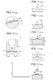
- Figs. 1(a) to 1(g) are views showing an example of the manufacturing process of the master die for manufacturing the die for optical element molding.
- a creation of the shape of the master transfer surface is not limited to the following method, but, for example, as shown by an example which will be described later, it may also be formed by the cutting processing.
- the master transfer surface 1a is formed on the master die material 1.
- a master transfer surface 1a it is preferable when its shape is determined considering the thickness of the function film which will be described later, or the thermal contraction of the raw material of the optical element, to the designed optical surface shape of the lens (an example of the optical element) desired to be formed by the die for optical element molding.
- the periphery of the master transfer surface 1a is a mother geometrical dimension reference surface 1b corresponding to a tilt reference plane.
- the resist R is coated on the master transfer surface 1a and the mother geometrical dimension reference surface 1b (spin coat).
- the resist R is coated with an equal film thickness on the master transfer surface 1a and on the upper surface of the master die material 1 including the mother geometrical dimension reference surface 1b.
- the electronic beam LB is irradiated by the exposing machine, and the minute pattern is exposure-formed. Succeedingly, as shown in Fig. 1(c), the master die material 1 is sintered in the solution, and on the master transfer surface 1a, the resist R is removed corresponding to the exposure-formed minute pattern.
- the beam diameter of the electronic beam LB is very small, and the exposure can be conducted at the interval of several-tens to several-hundreds nano-meter, the resist R can be removed corresponding to it.
- the upper surface of the master die material 1 from which the resist R is partially removed is exposed in the atmosphere of ion-shower IS (accelerated argon-ion) (dry etching), and corresponding to the pattern of the resist R, the surface of the master die material 1 is removed.
- ion-shower IS accelerated argon-ion
- dry etching dry etching
- a target T precious metal film, transition meal film, ceramics, or oxide ⁇ nitride ⁇ diamond
- the function film FM Fig. 1 (g)
- the function film FM is as thin as possible.
- the target T is changed to a predetermined composition one, and as shown in Fig. 1(e), from here, the amorphous alloy particles having the super-cooling liquid phase are scattered, and the film layer MG of 0.1 ⁇ m - 500 ⁇ m of the amorphous alloy having the super-cooling liquid phase is formed on the master transfer surface 1a (a process to form the film layer of the amorphous alloy having the super-cooling liquid phase).
- An enlarged view of the master transfer surface 1a after such a process is shown in Fig. 1(g).
- the master die material 1 formed in such a manner is fixed by a bolt 3 in a form to close one end of the tubular cylinder 2, and the master die 4 is formed (Fig. 1(f)). Between a cylinder 2 and the master die material 1, a groove 2a is formed on the end surface of the cylinder 2 so that an air vent is formed.
- a large-scale equipment is necessary, and its manufacturing cost is also high, however, when there is one equipment, because a large amount of the dies for optical element molding can be manufactured in the manner as will be described later, it is not particularly problem.
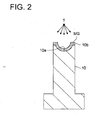
- Fig. 2 is a sectional view of the die for optical element molding.
- the base material 10 is formed from stainless steel.
- the material of the base material 10 is not particularly limited, however, commonly used die material such as steel or stainless steel is preferable, and in this case, there is a merit that a supply is stable and the price is low.
- the base material 10 as a blank corresponds to the optical surface (for example, aspheric surface) of the optical element in one end (in the view, an upper end), however, when the concave portion (shifted surface) 10a whose curvature is larger than it, or equal to it, and a peripheral surface 10b of its periphery are formed, it has the approximate shape of the metallic mold.
- the accuracy of the shape of the concave portion 10a and peripheral surface 10b depends on the film thickness of the amorphous alloy MG (hereinafter, simply called amorphous alloy) having the super-cooling liquid phase provided on the surface, however, when it is a case where the film of the amorphous alloy MG of about 100 ⁇ m is formed, and it has the accuracy of 10 - 20 ⁇ m, because it is enough, the blank processing itself takes a time period of about several-tens minutes by using a NC lathe. Onto this concave portion 10a and the peripheral surface 10b, the amorphous alloy MG having the super-cooling liquid phase is adhered in the following manner.
- amorphous alloy MG hereinafter, simply called amorphous alloy
- the amorphous alloy MG is film-formed on the surface of the concave portion 10a and the peripheral surface 10b, in the manner whose detail will be described later in examples, by the PVC processing such as spattering or vapor deposition, or Chemical vapor deposition method (a process to form the film layer of the amorphous alloy having the super-cooling liquid phase on the shifted surface).
- the composition of the film layer of the amorphous alloy having the super-cooling liquid phase can be same as that of the film layer formed on the master die material 1, or different from that.
- the amorphous alloy MG is film-formed, however, the film formation may be only on the concave portion 10a.
- the film formation of the amorphous alloy MG described above is, in Chemical vapor deposition method, because the master die material 1 or base material 10 becomes high temperature, disadvantageous in the characteristic of the amorphous alloy which is in a state of super-cooling liquid, however, the present invention is not limited to either one of Chemical vapor deposition method or Physical vapor deposition method.
- the Physical vapor deposition method by which the amorphous alloy MG is comparatively easily film-formed there is a processing such as spattering, ion plating, or vacuum evaporation, however, herein, any one may be used.
- the target material in the spattering method, may also be not always in the amorphous condition, and when the structuring atom is adhered in a desired composition ratio to the master die material 1 or base material 10, in the principle of the spattering, because the quick cooling is followed at the time of the adhering, the target material can be easily film-formed in the amorphous condition.
- the film formation speed is about 0.2 - several ⁇ m/h, and when the output of the spattering apparatus is increased, the time period of the film formation can be easily reduced, however, because the temperature of the master die material 1 or base material 10 is risen, and it does not become amorphous-like, the cooling of the master die material 1 or base material 10 by the water cooling becomes necessary.
- the amorphous alloy spread out in unnecessary part there is a possibility that the designed shape of_the die for optical element molding is damaged. Therefore, there is a case where it is necessary that the excepting part of the film formation part is masked, or after film formation, the spread out part is removed by the diamond cutting or grinding processing.
- the amorphous alloy MG is good in the machinability, and the removed amount is small, there is scarcely a burden of the processing man-hour or cost.
- the amorphous alloy MG when used for only a very limited part of the master die or the die for optical element molding in this manner, the amorphous alloy of the kind in which conventionally although having an excellent physical characteristic, the manufacturing of the bulk shape is difficult, can also be applied for the die for optical element molding.
- the highly hard amorphous alloy such as nickel-series or copper-series can be expected for the high durability as the metallic mold material, however, because it can hardly be brought into the bulk-like, by the method of the preceding application, the application to the die for optical element molding is difficult, however, as in the present embodiment, when the film is formed, the application becomes possible.
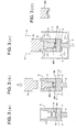
- Figs. 3(a) - 3(d) are views showing a formation process of the optical transfer surface of the die for optical element molding by the heating press and the geometrical dimension reference surface transfer surface.
- a support 5 is attached as shown in Fig. 3(a) to the master die 4 made in the process shown in Figs. 1(a) - 1(g).
- the master transfer surface 1a and the periphery of the mother geometrical dimension reference surface 1b are preliminarily heated by the heater H arranged in the periphery of the master die material 1, and the base material 10 made in the process shown in Fig. 2, is inserted into a cylinder 2, and pressed by a plunger 6 (heating press process).
- the air in the cylinder 2 flows out to the outside through an air vent (groove 2a).
- the amorphous alloy MG of the master die 4 which is heated higher than the glass transition point Tg, and the amorphous alloy MG of the base material 10 are fused with each other, and integrated.
- the amorphous alloy MG is quickly cooled.
- a cooling may also be a natural cooling.
- the function film FM when the function film FM remains on the master transfer surface 1a side, it functions as a protective film of the master die material 1, and when it is shifted to the base material 10 side together with the amorphous alloy MG, it functions as a protective film of the metallic mold.
- the function film FM when, as the raw material of the function film FM, for example, a material which is dissipated by the heat, is used, after the function film FM is opened to the air, when passing through a process by which it is heated and removed, the accurate optical element can be obtained.
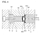
- Fig. 4 is a sectional view of a die-set including the die for optical element molding for forming the lens which is an example of the optical element.
- the die for optical element molding 10' on which the amorphous alloy MG is film-formed and the die for optical element molding 11' on which the amorphous alloy MG' is film-formed in the same manner are inserted into the die-set metallic molds 13, 14, so that mutual optical surface transfer surfaces MGa, MGa' and mutual geometrical dimension reference surface transfer surfaces MGb, MGb' are faced each other, and when the fused plastic material PL is injected from a gate, not shown, between the die for optical element moldings 10', 11', in the same manner as the ordinal injection molding, and further, cooled, a lens having a desired shape can be obtained.
- the optical surface transfer surface MGa or geometrical dimension reference surface transfer surface MGb is created by the heating press molding, it is enough when a part on which the amorphous alloy MG is film-formed is preponderantly heated and softened, and pressed to the heated master die 1.
- the amorphous ally MG is not used for the entire die for optical element molding 10', but limited to be used for only a layer forming the optical surface transfer surface MGa or geometrical dimension reference surface transfer surface MGb and only its periphery, and it is not necessary that the entire base material 10 is uniformly heated.
- the temperature control can also be accurately conducted, and because the press deformation amount is also small, the pressing time period can be very much reduced.
- the crystallization is not concerned about, and the heating press molding can be retried any number of times, thereby, the shape correction of the optical surface transfer surface MGa or recycle can be conducted without melting-down, further, also for a certain kind of amorphous alloy in which, although it has the excellent physical characteristic, the heating press molding can not be conducted for a reason that it is easily crystallized, it can be applied for the die for optical element molding.
- the atmosphere of the heating press molding it is preferable that, ordinarily, it is conducted in the vacuum in order to prevent the oxidation of the amorphous alloy or the crystallization according to that, and because, even when palladium amorphous alloy is heated in the air, the alloy is hardly oxidized, the heating press molding can be conducted in the air.
- the heating press molding apparatus does not need to keep the vacuum atmosphere, it can be made further simple, and there is a merit that the heating press molding can be conducted in the air while being directly visually observed.
- palladium amorphous alloy there is Pd 40 Cu 30 Ni 10 P 20 or Pd 76 Cu 6 Si 18 , Pd 61 Pt 15 Cu 6 Si 18 , however, when palladium is not contained at least more than 20 mol %, the other composition atom is brought to be oxidized or easily crystallized, and the heating press molding in the air becomes difficult. On the one hand, when the containing amount of palladium is more than 80 mol %, generally, the glass transition point does not exist, and the amorphous alloy is not formed.
- the amorphous alloy in which the heating press molding is stably conducted in the air it is preferable that palladium containing amount is not smaller than 20 mol % and not larger than 80 mol %. Further, when viewed from the composition atom other than palladium which is the maximum containing atom, it is necessary that any one of Cu, Ni, Al, Si, Pd, Br is contained more than one at least more than 3 mol %, for forming the amorphous-like amorphous alloy.
- the amorphous alloy of the precious metal such as palladium series is used for the die for optical element molding, because there is a precious bare metal value by only one of metallic molds, in the molding production process of the optical element, in order to treat a lot of such precious and small parts, a problem in the security that the storage control is made severe, is inevitable.
- the film thickness of the amorphous alloy can be made to abut 100 ⁇ m, and the bare metal value is merely comma several %, there is a very important practical characteristic to the technology of the preceding application in which the storage control may be the same as the conventional one.
- the chemical plating processing as in the conventional metallic mold is not necessary at all, and the optical surface transfer surface can be created highly accurately and efficiently, and accordingly, there is an excellent characteristic in which, although the high accurate optical surface of the optical element can be transfer-molded, it is low cost and short delivery time period and can be handled in the same production form as the conventional one. Further, the metallic mold for molding of the optical element having the minute structure can also be easily created.
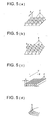
- Figs. 5(a) - 5(d) are perspective views enlargedly showing an example of the optical surface of a lens formed by such a die for optical element molding.
- a structure an example of the minute structure of the equivalent refractive index area in which, on the optical surface of the lens, as an example of a plurality of protrusions, a many number of minute cylinders C are matrix-likely formed, is shown.
- the wavelength of the light transmitting the lens is about 650 nm. Accordingly, when the interval ⁇ of the minute cylinder C is 160 nm, the light incident on such an objective lens is slightly reflected, and the objective lens whose light transmission is very high, can be provided.
- a large number of minute triangle cones T separated by the interval ⁇ are formed, and it has the same remarkable effect as Fig. 5(a).
- this interval ⁇ when it is not larger than 0.1 - 0.2 ⁇ m, it is preferable because scattering is lowered.
- a large number of fins F an example of the minute structure of the structure double refraction separated by the interval ⁇ are formed. The length of fin F is longer than the wavelength of the transmitting light (in the above example, not smaller than 650 ⁇ m).
- the lens provided with such a structure transmits the light having the oscillation surface in the direction along the fin F, however, a so-called polarizing effect that the light in the direction crossing the fin F is not transmitted is taken.
- a so-called polarizing effect that the light in the direction crossing the fin F is not transmitted is taken.
- the blaze type diffraction ring-shaped zone D whose section in the optical axis direction is saw-tooth-like, is formed.
- the chromatic aberration correction and the temperature correction which are effects corresponding to the shape, are described in detail, for example, in Tokkai No. 2001-195769, the description hereafter will be neglected.
- NPS NPS
- DOE can also be formed.
- the bottom surface is made a curved surface having an appropriate curvature of the spherical surface or aspheric surface, and the protrusions may also be provided on the curved surface.
- a comparative example carried out by the present inventors will be described below.
- a base material of the die for the optical element molding of about 3 - 5 mm diameter
- a material in which iron is contained in main component, and which can be easily cut is prepared.
- 5 blank metallic molds (called also base material of the metallic mold) are manufactured by cutting ⁇ grinding processing.
- a die base material surface of the blank metallic mold is (grinding ⁇ cutting) processed in the shape accuracy not larger than 100 ⁇ m, and the concave surface corresponding to the aspheric surface of the optical element is formed.
- the film layers of the amorphous alloy having the super-cooling liquid phase between 295 - 396 °C are respectively formed in the film thickness of 0.02, 10, 50, 100, 500 ⁇ m.
- the master die initially, as the master die material of the die for the optical element molding of about 3 - 5 mm diameter, a material in-which iron is contained in main component, and which can be easily cut, is prepared.
- the master die material is manufactured by cutting ⁇ grinding processing.
- the master transfer surface of the master die material is (grinding ⁇ cutting) processed in the shape accuracy of not larger than 100 ⁇ m.
- the electroless nickel plating is film-formed in the thickness of about 100 ⁇ m. This plated master die molding transfer surface is cut by the diamond tool, and the master die is completed.
- the master die in which the amorphous alloy film layer is not formed is arranged facing the raw material of the metallic mold in which the amorphous alloy film layer having the super-cooling liquid phase between 295 - 395 °C is formed, and heated to 310 °C more than the glass transition point, and by press molding for one hour under a force of 300 N, the shape and structure of the master transfer surface of the master die are transferred onto the amorphous alloy film layer of the raw material of the metallic mold.
- a large amount of high accurate metallic molds can be obtained only by simple processes of heating and pressing.
- the minute structure for example, blazé shape
- the heating press pressure is too high (more than 500 N, particularly, a case where a half part of it is touched, inclined and brought into contact with the die)
- the temperature of a part of the amorphous alloy film layer in contact with the master transfer surface does not arrive to the glass transition temperature, there is a possibility that the minute structure or the master die shape is broken.
- the master transfer surface of the master die on which the amorphous alloy film layer is formed and the base material (or, base material of the metallic mold on which the amorphous alloy film layer having the super-cooling liquid phase is formed) are oppositely arranged, and in the atmosphere (about 100 Pa) substituted by He-gas, when it is heated to 310 °C which is more than the glass transition point, and press-molded under 200 N for one hour, the amorphous alloy film layer formed on the master transfer surface of the master die is peeled form the master die, and transferred onto the base material (or, onto the base material on which the amorphous alloy film layer having the super-cooling liquid phase is formed) of the metallic mold, (for the above 5-kinds of the film thickness of the amorphous alloys on the master die, it is conducted in the same manner).
- the temperature of the master die is 330 °C
- the temperature of the base material of the metallic mold is 300 °C, although they are more than Tg
- the thermal gradient is provided, it becomes a good condition in a point of releasing from the master die and an increase of the adhesion to the die material.
- the heat control can be effectively conducted, and the heater output can be greatly utilized.
- the manufacturing method of the die for optical element molding because it is not the shape transfer by the dynamic molding method, but the transfer by the reversal shape by the film formation method such as the spattering, it can be seen that any of minute shapes of the master die can also be transferred, and there is no damage of the die.
- the film thickness of the amorphous alloy formed on the master die are distributed as described above, the same effect can be obtained.
- a manufacturing method of the die for optical element molding by which the accuracy of dimension of the optical element can be increased although the manufacture is easy, can be provided.
Landscapes
- Engineering & Computer Science (AREA)
- Chemical & Material Sciences (AREA)
- Organic Chemistry (AREA)
- Manufacturing & Machinery (AREA)
- Materials Engineering (AREA)
- Mechanical Engineering (AREA)
- Biochemistry (AREA)
- Life Sciences & Earth Sciences (AREA)
- Health & Medical Sciences (AREA)
- Bioinformatics & Cheminformatics (AREA)
- General Engineering & Computer Science (AREA)
- General Health & Medical Sciences (AREA)
- Genetics & Genomics (AREA)
- Wood Science & Technology (AREA)
- Zoology (AREA)
- Moulds For Moulding Plastics Or The Like (AREA)
- Diffracting Gratings Or Hologram Optical Elements (AREA)
Abstract
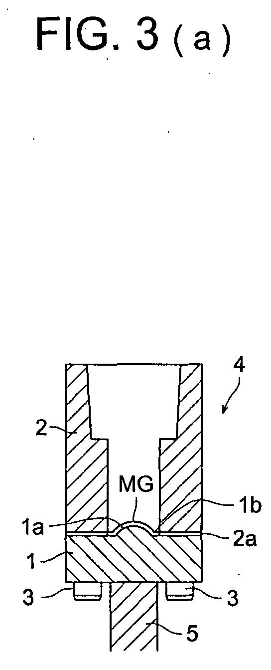
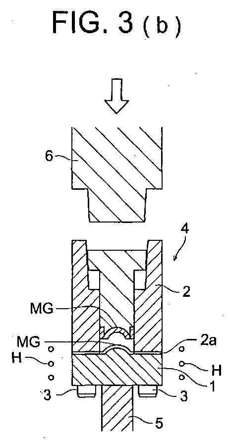
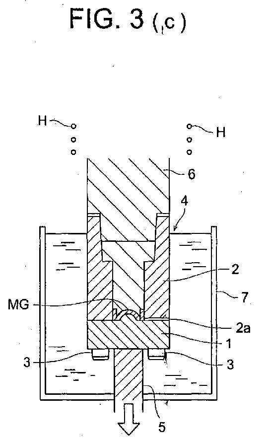
Description
As this interval Δ, when it is not larger than 0.1 - 0.2 µm, it is preferable because scattering is lowered. In Fig. 5(c), on the optical surface of the lens, as an example of a plurality of protrusions, a large number of fins F (an example of the minute structure of the structure double refraction) separated by the interval Δ are formed. The length of fin F is longer than the wavelength of the transmitting light (in the above example, not smaller than 650 µm). The lens provided with such a structure transmits the light having the oscillation surface in the direction along the fin F, however, a so-called polarizing effect that the light in the direction crossing the fin F is not transmitted is taken. In Fig. 5(d), on the optical surface of the lens, as an example of the ring-shaped zone structure around the optical axis, the blaze type diffraction ring-shaped zone D whose section in the optical axis direction is saw-tooth-like, is formed. For the diffraction ring-shaped zone D, because the chromatic aberration correction and the temperature correction, which are effects corresponding to the shape, are described in detail, for example, in Tokkai No. 2001-195769, the description hereafter will be neglected. As the other ring-shaped zone structure, NPS, DOE can also be formed. Further, in Figs. 5(a) - (c), an example in which those protrusions are provided on the plane is shown in order to simply describe it, however, the bottom surface is made a curved surface having an appropriate curvature of the spherical surface or aspheric surface, and the protrusions may also be provided on the curved surface.
Claims (58)
- A manufacturing method of a die for molding an optical element, the manufacturing method comprising:forming the first film layer of an amorphous alloy having a super-cooling liquid phase onto a master transfer surface of a master die for molding a molding transfer surface of the die;heating the first film layer to more than a glass transition point of the amorphous alloy having the super-cooling liquid phase while a surface of the first film layer and a transferred surface of a base material of the die are being faced and pressed; andpeeling the first film layer from the master die and transferring the first film layer onto the base material of the die to form the molding transfer surface of the die.
- The manufacturing method of claim 1, wherein, in the step of forming the first film layer on the master transfer surface of the master die, the film thickness of the first film layer is 0.01 - 500 µm.
- The manufacturing method of claim 1 or 2, wherein the manufacturing method further comprises forming a second film layer of an amorphous alloy having a super-cooling liquid phase on the transferred surface of the base material of the die before the step of peeling the first film layer from the master die and transferring the first film layer onto the base material of the die, and
wherein, in the step of transferring the first film layer onto the base material of the die, at least one of the first film layer and the second film layer is heated above the glass transition point of at least one of the amorphous alloy having the super-cooling liquid phase of the first film layer and the amorphous alloy having the super-cooling liquid phase of the second film layer while the first film layer and the second film layer are faced and being pressed. - The manufacturing method of claim 3, wherein a composition of the amorphous alloy having the super-cooling liquid phase of the first film layer and the composition of the amorphous alloy having the super-cooling liquid phase of the second film layer are the same.
- The manufacturing method of claim 3, wherein a composition of the amorphous alloy having the super-cooling liquid phase of the first film layer and the composition of the amorphous alloy having the super-cooling liquid phase of the second film layer are different from each other.
- The manufacturing method of claim 3, 4 or 5, wherein the film thickness of the second film layer is 0.01 - 500 µm.
- The manufacturing method according to any one of the preceding claims, wherein the manufacturing method further comprises providing a first function film on the master transfer surface of the master die, before the step of forming the first film layer of the amorphous alloy having the super-cooling liquid phase on the master transfer surface of the master die.
- The manufacturing method of claim 7, wherein the film thickness of the first function film is 0.01 - 20 µm.
- The manufacturing method of claim 7 or 8, wherein the first function film contains at least one kind of substance selected from the group consisting of precious metal elements of Pt, Ir, Pd, Au, Ru, Rh, and Ag, the transition metal elements of Fe, Co, Ni, Cr, W, Ti, Mo and Zr, alumina, chromina, tungsten carbide, silicon nitride, carbon nitride, TiN, TiAlN, zirconia, diamond, diamond-like carbon and carbon.
- The manufacturing method of claim 7, 8 or 9, wherein the first function film contains at least one kind of element selected from the group consisting of the precious metal elements of Pt, Ir, Pd, Au, Ru, Rh and Ag, and the transition metal elements of Fe, Co, Ni, Cr, W, Ti, Mo and Zr.
- The manufacturing method according to any one of claims 7 to 10, wherein the first function film contains at least one kind of raw material selected from the group consisting of alumina, chromina, tungsten carbide, silicon nitride, carbon nitride, TiN, TiAlN, zirconia, diamond, diamond-like carbon and carbon.
- The manufacturing method according to any one of claims 7 to 11, wherein the manufacturing method further comprises providing a second function film on the first function film, before the step of forming the first film layer of the amorphous alloy having the super-cooling liquid phase onto the master transfer surface of the master die.
- The manufacturing method of claim 12, wherein the film thickness of the second function film is 0.01 - 20 µm.
- The manufacturing method of claim 12 or 13, wherein the second function film contains at least one kind of substance selected from the group consisting of precious metal elements of Pt, Ir, Pd, Au, Ru, Rh and Ag, transition metal elements of Fe, Co, Ni, Cr, W, Ti, Mo and Zr, alumina, chromina, tungsten carbide, silicon nitride, carbon nitride, TiN, TiAlN, zirconia, diamond, diamond-like carbon and carbon.
- The manufacturing method of claim 12, 13 or 14, wherein the second function film contains at least one kind of element selected from the group consisting of the precious metal elements of Pt, Ir, Pd, Au, Ru, Rh and Ag and the transition metal elements of Fe, Co, Ni, Cr, W, Ti, Mo and Zr.
- The manufacturing method according to any one of claims 12 to 15, wherein the second function film contains at least one kind of raw material selected from the group consisting of alumina, chromina, tungsten carbide, silicon nitride, carbon nitride, Tin, TiA1N, zirconia, diamond, diamond-like carbon and carbon.
- The manufacturing method according to any one of claims 7 to 16, wherein the first function film is formed by one or more of the following methods:a vapor deposition method;a chemical vapor deposition method;a physical vapor deposition method;a spattering method;an ion-plating method; anda vacuum evaporation method.
- The manufacturing method according to any one of claims 7 to 17, wherein the optical shape of the master transfer surface of the master die is made to be different from a shape of an optical surface of an optical element, which is formed by the molding transfer surface of the die, the molding transfer surface being formed by the master transfer surface, and
wherein the difference is determined in accordance with at least one of the thickness of the first function film formed on the master transfer surface and a heat contraction of an optical element material. - The manufacturing method according to any one of claims 7 to 18, wherein the first function film remains on the master transfer surface after the steps of peeling the first film layer from the master die and transferring the first film layer onto the base material of the die.
- The manufacturing method according to any one of claims 7 to 19, wherein the first function film is transferred onto the molding transfer surface of the die after the steps of peeling the first film layer from the master die and transferring the first film layer onto the base material of the die.
- The manufacturing method of claim 20, wherein the manufacturing method further comprises removing the first function film transferred onto the molding transfer surface of the die.
- The manufacturing method according to any one of the preceding claims, wherein a ring-shaped zone structure around an optical axis of the optical element is formed on an optical surface of the optical element formed by the molding transfer surface of the die.
- The manufacturing method of claim 22, wherein the ring-shaped zone structure is an optical path difference-generating structure.
- The manufacturing method of claim 22 or 23, wherein the ring-shaped zone structure is a blaze type diffractive structure whose sectional shape in the optical axis direction is sawtooth shape.
- The manufacturing method of claim 22, 23 or 24, wherein the ring-shaped zone structure is the diffractive structure whose sectional shape including the optical axis is step-like shape.
- The manufacturing method according to any one of claims 22 to 25, wherein the optical element is used in an optical pickup apparatus, and the ring-shaped zone structure has a function by which an aberration change of the optical element due to a wavelength change of a light source to irradiate light onto the optical element is corrected.
- The manufacturing method according to any one of claims 22 to 26, wherein the ring-shaped zone structure has a function by which an aberration change due to a temperature change of the optical element is corrected.
- The manufacturing method according to any one of the preceding claims, wherein a plurality of protrusions or hollows are formed on the molding transfer surface of the die by a plurality of protrusions or hollows formed on the master transfer surface of the master die so that a plurality of protrusions or hollows corresponding to the protrusions or hollows on the molding transfer surface of the die are formed on an optical surface of the optical element.
- The manufacturing method of claim 28, wherein the protrusions or hollows of the optical surface of the optical element form a minute structure of an equivalent refractive index area.
- The manufacturing method of claim 28 or 29, wherein the protrusions or hollows of the optical surface of the optical element form a minute structure, which generates a reflection prevention effect.
- The manufacturing method of claim 28, 29 or 30, wherein the protrusions or hollows of the optical surface of the optical element form a minute structure, which generates a structure double refraction.
- The manufacturing method according to any one of claims 28 to 31, wherein the protrusions or hollows of the optical surface of the optical element form the minute structure of the resonance area.
- The manufacturing method according to any one of claims 28 to 32, wherein the protrusions or hollows on the molding transfer surface of the die are formed on a part of the molding transfer surface of the die so that the protrusions or hollows of the optical surface of the optical element are formed on a part of the optical surface.
- The manufacturing method according to any one of the preceding claims, wherein the protrusions or hollows formed on the molding transfer surface of the die is formed on a part of the molding transfer surface of the die so that the protrusions or hollows of the optical surface of the optical element include at least a plurality of shapes or arrangement patterns and are formed on a part of the optical surface of the optical element.
- The manufacturing method according to any one of the preceding claims, wherein the molding transfer surface of the die is formed of only the aspheric surface shape.
- The manufacturing method according to any one of the preceding claims, wherein the first film layer is formed by a vacuum evaporation method.
- The manufacturing method of claim 36, wherein the first film layer is formed by one or more of the following methods:a chemical vapor deposition method;a physical vapor deposition method;a spattering method;an ion-plating method; anda vacuum evaporation method.
- The manufacturing method according to any one of the preceding claims, wherein the composition of the amorphous alloy having the super-cooling liquid phase of the first film layer contains Pd in the rate of not smaller than 20 mol% and not larger than 90 mol%.
- The manufacturing method of claim 38, wherein the composition of the amorphous alloy having the super-cooling liquid phase of the first film layer contains at least one kind of element selected from the group consisting of Cu, Ni, Al, Si, P and B in a rate of not smaller than 1 mol%.
- The manufacturing method according to any one of the preceding claims, wherein composition of the amorphous alloy having the super-cooling liquid phase of the first film layer contains Zr in the rate of not smaller than 20 mol% and not larger than 90 mol%.
- The manufacturing method of claim 40, wherein the composition of the amorphous alloy having the super-cooling liquid phase of the first film layer contains at least one kind of element selected from the group consisting of Fe, Co, Hf, Ti, Cu, Ni, Al, Sn, Si, P and B in a rate of not smaller than 1 mol%.
- The manufacturing method according to any one of the preceding claims, wherein the composition of the amorphous alloy having the super-cooling liquid phase of the first film layer contains Ti in the rate of not smaller than 20 mol% and not larger than 90 mol%.
- The manufacturing method of claim 42, wherein the composition of the amorphous alloy having the super-cooling liquid phase of the first film layer contains at least one kind of element selected from the group consisting of Hf, Zr, Cu, Ni, Co, Fe, Sn, Al, Si, P and B in a rate of not smaller than 1 mol%.
- The manufacturing method according to any one of the preceding claims, wherein the composition of the amorphous alloy having the super-cooling liquid phase of the first film layer contains Mg in the rate of not smaller than 20 mol% and not larger than 90 mol%.
- The manufacturing method of claim 44, wherein the composition of the amorphous alloy having the super-cooling liquid phase of the first film layer contains at least one kind of element selected from the group consisting of Y, Hf, Zr, Cu, Fe, Co, Ni, Al, Si, P and B in a rate of not smaller than 1 mol%.
- The manufacturing method according to any one of the preceding claims, wherein the composition of the amorphous alloy having the super-cooling liquid phase of the first film layer contains La in the rate of not smaller than 20 mol% and not larger than 90 mol%.
- The manufacturing method of claim 46, wherein the composition of the amorphous alloy having the super-cooling liquid phase of the first film layer contains at least one kind of element selected from the group consisting of Cu, Ni, Co, Al, Si, P, B, Hf and Zr in a rate of not smaller than 1 mol%.
- The manufacturing method according to any one of the preceding claims, wherein the composition of the amorphous alloy having the super-cooling liquid phase of the first film layer contains Fe in the rate of not smaller than 20 mol% and not larger than 90 mol%.
- The manufacturing method of claim 48, wherein the composition of the amorphous alloy having the super-cooling liquid phase of the first film layer contains at least one kind of element selected from the group consisting of Co, Ni, Hf, Zr, Ti, Cu, Ni, Al, Sn, Si, P and B in a rate of not smaller than 1 mol%.
- The manufacturing method according to any one of the preceding claims, wherein the composition of the amorphous alloy having the super-cooling liquid phase of the first film layer contains Co in the rate of not smaller than 20 mol% and not larger than 90 mol%.
- The manufacturing method of claim 50, wherein the composition of the amorphous alloy having the super-cooling liquid phase of the first film layer contains at least one kind of element selected from the group consisting of Ni, Hf, Fe, Zr, Ti, Cu, Ni, Al, Sn, Si, P and B in a rate of not smaller than 1 mol%.
- The manufacturing method according to any one of the preceding claims, wherein the composition of the amorphous alloy having the super-cooling liquid phase of the first film layer contains Ni in the rate of not smaller than 20 mol% and not larger than 90 mol%.
- The manufacturing method of claim 52, wherein the composition of the amorphous alloy having the super-cooling liquid phase of the first film layer contains at least one kind of element selected from the group consisting of Co, Hf, Fe, Zr, Ti, Cu, Ni, Al, Sn, Si, P and B in a rate of not smaller than 1 mol%.
- The manufacturing method according to any one of the preceding claims, wherein the composition of the amorphous alloy having the super-cooling liquid phase of the first film layer contains Mo in the rate of not smaller than 20 mol% and not larger than 90 mol%.
- The manufacturing method of claim 54, wherein the composition of the amorphous alloy having the super-cooling liquid phase of the first film layer contains at least one kind of element selected from the group consisting of Fe, Co, Ni, Cu, Hf, Zr, Ti, W, Sn, Al, Si, P, B and Pd in a rate of not smaller than 1 mol%.
- The manufacturing method according to any one of the preceding claims, wherein the composition of the amorphous alloy having the super-cooling liquid phase of the first film layer contains Pt in the rate of not smaller than 20 mol% and not larger than 90 mol%.
- The manufacturing method of claim 56, wherein the composition of the amorphous alloy having the super-cooling liquid phase of the first film layer contains at least one kind of element selected from the group consisting of Fe, Co, Ni, Cu, Hf, Zr, Ti, W, Sn, Al, Si, P, B and Pd in a rate of not smaller than 1 mol%.
- The manufacturing method according to any one of the preceding claims, wherein the composition of the amorphous alloy having the super-cooling liquid phase of the first film layer contains at least one kind of precious metal element selected from the group consisting of Os, Pt, Ir, Au, Ag, Rh, Pd and Ru in a rate of not smaller than 1 mol%.
Applications Claiming Priority (2)
| Application Number | Priority Date | Filing Date | Title |
|---|---|---|---|
| JP2004104251 | 2004-03-31 | ||
| JP2004104251 | 2004-03-31 |
Publications (3)
| Publication Number | Publication Date |
|---|---|
| EP1604757A2 true EP1604757A2 (en) | 2005-12-14 |
| EP1604757A3 EP1604757A3 (en) | 2005-12-21 |
| EP1604757B1 EP1604757B1 (en) | 2008-12-24 |
Family
ID=35044956
Family Applications (1)
| Application Number | Title | Priority Date | Filing Date |
|---|---|---|---|
| EP05251886A Expired - Lifetime EP1604757B1 (en) | 2004-03-31 | 2005-03-24 | Manufacturing method of die for optical element molding |
Country Status (8)
| Country | Link |
|---|---|
| US (1) | US7366395B2 (en) |
| EP (1) | EP1604757B1 (en) |
| JP (1) | JP4525677B2 (en) |
| KR (1) | KR101139071B1 (en) |
| CN (1) | CN1676477B (en) |
| DE (1) | DE602005011892D1 (en) |
| TW (1) | TWI346092B (en) |
| WO (1) | WO2005097450A1 (en) |
Cited By (1)
| Publication number | Priority date | Publication date | Assignee | Title |
|---|---|---|---|---|
| RU2457185C1 (en) * | 2011-02-11 | 2012-07-27 | Открытое акционерное общество "Обнинское научно-производственное предприятие "Технология" | Device for extrusion of hollow glass articles |
Families Citing this family (38)
| Publication number | Priority date | Publication date | Assignee | Title |
|---|---|---|---|---|
| US7488170B2 (en) * | 2004-04-09 | 2009-02-10 | Konica Minolta Opto, Inc. | Metallic mold for optical element and optical element |
| WO2007046437A1 (en) * | 2005-10-19 | 2007-04-26 | The Circle For The Promotion Of Science And Engineering | Corrosion-resistant heat-resistant alloy for molding die and die for molding optical device |
| JP4753249B2 (en) * | 2006-01-13 | 2011-08-24 | 株式会社神戸製鋼所 | Mold for glass molding |
| CN101675174A (en) * | 2007-02-13 | 2010-03-17 | 耶鲁大学 | Method for imprinting and erasing amorphous metal alloys |
| JP2009280410A (en) * | 2008-04-21 | 2009-12-03 | Konica Minolta Opto Inc | Mold for forming glass substrate, method of manufacturing glass substrate, method of manufacturing glass substrate for information recording medium, method of manufacturing information recording medium, glass substrate for information recording medium, and information recording medium |
| TW201111144A (en) | 2009-09-30 | 2011-04-01 | E Pin Optical Industry Co Ltd | High sag optical lens and method for fast molding the same |
| US8459331B2 (en) | 2011-08-08 | 2013-06-11 | Crucible Intellectual Property, Llc | Vacuum mold |
| US8858868B2 (en) | 2011-08-12 | 2014-10-14 | Crucible Intellectual Property, Llc | Temperature regulated vessel |
| JP5941253B2 (en) * | 2011-08-22 | 2016-06-29 | 株式会社小糸製作所 | Vehicle lamp |
| JP5723078B2 (en) | 2011-11-11 | 2015-05-27 | クルーシブル インテレクチュアル プロパティ エルエルシーCrucible Intellectual Property Llc | Dual plunger rod for controlled transfer in injection molding system |
| US9302320B2 (en) | 2011-11-11 | 2016-04-05 | Apple Inc. | Melt-containment plunger tip for horizontal metal die casting |
| US20130125590A1 (en) * | 2011-11-23 | 2013-05-23 | Jiangwei Feng | Reconditioning glass-forming molds |
| CN102615820A (en) * | 2012-04-12 | 2012-08-01 | 中国科学院物理研究所 | Metallic glass-based plastic thermal embossing micro-molding mold and preparation method thereof |
| US9314839B2 (en) | 2012-07-05 | 2016-04-19 | Apple Inc. | Cast core insert out of etchable material |
| US8701742B2 (en) | 2012-09-27 | 2014-04-22 | Apple Inc. | Counter-gravity casting of hollow shapes |
| US9004151B2 (en) | 2012-09-27 | 2015-04-14 | Apple Inc. | Temperature regulated melt crucible for cold chamber die casting |
| US8826968B2 (en) | 2012-09-27 | 2014-09-09 | Apple Inc. | Cold chamber die casting with melt crucible under vacuum environment |
| US8833432B2 (en) | 2012-09-27 | 2014-09-16 | Apple Inc. | Injection compression molding of amorphous alloys |
| US8813816B2 (en) | 2012-09-27 | 2014-08-26 | Apple Inc. | Methods of melting and introducing amorphous alloy feedstock for casting or processing |
| US8813814B2 (en) | 2012-09-28 | 2014-08-26 | Apple Inc. | Optimized multi-stage inductive melting of amorphous alloys |
| US8813813B2 (en) | 2012-09-28 | 2014-08-26 | Apple Inc. | Continuous amorphous feedstock skull melting |
| US8813817B2 (en) | 2012-09-28 | 2014-08-26 | Apple Inc. | Cold chamber die casting of amorphous alloys using cold crucible induction melting techniques |
| US10197335B2 (en) | 2012-10-15 | 2019-02-05 | Apple Inc. | Inline melt control via RF power |
| JP6199086B2 (en) * | 2013-06-13 | 2017-09-20 | 東洋鋼鈑株式会社 | Palladium-plated coating material and method for producing palladium-plated coating material |
| US9925583B2 (en) | 2013-07-11 | 2018-03-27 | Crucible Intellectual Property, Llc | Manifold collar for distributing fluid through a cold crucible |
| US9445459B2 (en) | 2013-07-11 | 2016-09-13 | Crucible Intellectual Property, Llc | Slotted shot sleeve for induction melting of material |
| CA2928616A1 (en) | 2013-10-28 | 2015-05-07 | Toyo Kohan Co., Ltd. | Alloy plate coated material and method of producing alloy plate coated material |
| JP6411734B2 (en) * | 2013-12-12 | 2018-10-24 | Hoya株式会社 | Mold for glass optical element blank for polishing, glass optical element blank for polishing, and method for producing optical element |
| US20150175467A1 (en) * | 2013-12-23 | 2015-06-25 | Infineon Technologies Austria Ag | Mold, method for producing a mold, and method for forming a mold article |
| CN103774109B (en) * | 2014-01-26 | 2016-06-08 | 浙江大学 | A kind of supersensitive Fe-Y-B metallic film and preparation method thereof |
| AT14576U1 (en) * | 2014-08-20 | 2016-01-15 | Plansee Se | Metallization for a thin film device, method of making the same and sputtering target |
| US9873151B2 (en) | 2014-09-26 | 2018-01-23 | Crucible Intellectual Property, Llc | Horizontal skull melt shot sleeve |
| CN104730674A (en) * | 2015-02-10 | 2015-06-24 | 华南理工大学 | Manufacturing method for LED optical lens and mold of LED optical lens |
| CN111629876A (en) * | 2017-12-19 | 2020-09-04 | 豪雅镜片泰国有限公司 | Method for manufacturing spectacle lens molding die and method for manufacturing spectacle lens |
| CN111847852B (en) * | 2020-07-23 | 2023-11-14 | 北方夜视技术股份有限公司 | Spherical forming system and method for lobster eye optical device |
| CN112062450B (en) * | 2020-08-31 | 2022-05-27 | 深圳大学 | Preparation method of amorphous glass hot-pressing mold and hot-pressing mold |
| EP4122689B1 (en) * | 2021-07-20 | 2026-04-29 | Essilor International | Low thermal conductivity metal insert with surface microstructures |
| CN118023841A (en) * | 2024-01-08 | 2024-05-14 | 南宁燎旺车灯股份有限公司 | A processing method to avoid cutting marks on parts |
Family Cites Families (13)
| Publication number | Priority date | Publication date | Assignee | Title |
|---|---|---|---|---|
| JP3147481B2 (en) * | 1992-04-21 | 2001-03-19 | 松下電器産業株式会社 | Mold for forming glass diffraction grating, method for manufacturing the same, and method for manufacturing glass diffraction grating |
| JPH0725628A (en) * | 1993-07-09 | 1995-01-27 | Matsushita Electric Ind Co Ltd | Mold for molding fine optical glass element and method for manufacturing the same |
| JPH07172849A (en) * | 1993-12-16 | 1995-07-11 | Matsushita Electric Ind Co Ltd | Mold for press-molding optical element and method for manufacturing the same |
| JPH07307553A (en) * | 1994-05-11 | 1995-11-21 | Nitto Denko Corp | Method for forming metal thin film on metal substrate |
| CN1292770A (en) * | 1999-01-05 | 2001-04-25 | 松下电器产业株式会社 | Die for forming optical device, method for manufacturing the same, and optical device |
| US20020118465A1 (en) * | 2001-02-28 | 2002-08-29 | Konica Corporation | Molding die for optical element, optical element and master die |
| JP4203709B2 (en) * | 2001-02-28 | 2009-01-07 | コニカミノルタホールディングス株式会社 | Optical element mold |
| JP2002326230A (en) * | 2001-05-07 | 2002-11-12 | Ricoh Co Ltd | Mold manufacturing method and apparatus, mold and molded product |
| JP3964188B2 (en) * | 2001-11-20 | 2007-08-22 | 明 下河辺 | Mold for optical element molding |
| JP4110506B2 (en) * | 2001-11-21 | 2008-07-02 | コニカミノルタホールディングス株式会社 | Mold for optical element molding |
| JP2003251552A (en) * | 2002-02-27 | 2003-09-09 | Nikon Corp | Processing method, optical element and mold manufacturing method, optical element and optical device |
| JP2005173558A (en) * | 2003-11-21 | 2005-06-30 | Seiko Epson Corp | Circumferential surface processing method, developing roller and photosensitive drum manufacturing method, developing roller and photosensitive drum |
| US7488170B2 (en) * | 2004-04-09 | 2009-02-10 | Konica Minolta Opto, Inc. | Metallic mold for optical element and optical element |
-
2005
- 2005-03-24 TW TW094109132A patent/TWI346092B/en not_active IP Right Cessation
- 2005-03-24 WO PCT/JP2005/005314 patent/WO2005097450A1/en not_active Ceased
- 2005-03-24 JP JP2006512000A patent/JP4525677B2/en not_active Expired - Fee Related
- 2005-03-24 DE DE602005011892T patent/DE602005011892D1/en not_active Expired - Lifetime
- 2005-03-24 EP EP05251886A patent/EP1604757B1/en not_active Expired - Lifetime
- 2005-03-28 CN CN2005100624129A patent/CN1676477B/en not_active Expired - Fee Related
- 2005-03-28 KR KR1020050025444A patent/KR101139071B1/en not_active Expired - Fee Related
- 2005-03-28 US US11/090,232 patent/US7366395B2/en not_active Expired - Fee Related
Cited By (1)
| Publication number | Priority date | Publication date | Assignee | Title |
|---|---|---|---|---|
| RU2457185C1 (en) * | 2011-02-11 | 2012-07-27 | Открытое акционерное общество "Обнинское научно-производственное предприятие "Технология" | Device for extrusion of hollow glass articles |
Also Published As
| Publication number | Publication date |
|---|---|
| EP1604757B1 (en) | 2008-12-24 |
| DE602005011892D1 (en) | 2009-02-05 |
| KR20060044839A (en) | 2006-05-16 |
| TWI346092B (en) | 2011-08-01 |
| KR101139071B1 (en) | 2012-04-30 |
| JPWO2005097450A1 (en) | 2008-02-28 |
| TW200602274A (en) | 2006-01-16 |
| US7366395B2 (en) | 2008-04-29 |
| CN1676477B (en) | 2010-05-26 |
| JP4525677B2 (en) | 2010-08-18 |
| EP1604757A3 (en) | 2005-12-21 |
| US20050242454A1 (en) | 2005-11-03 |
| WO2005097450A1 (en) | 2005-10-20 |
| CN1676477A (en) | 2005-10-05 |
Similar Documents
| Publication | Publication Date | Title |
|---|---|---|
| EP1604757B1 (en) | Manufacturing method of die for optical element molding | |
| US7488170B2 (en) | Metallic mold for optical element and optical element | |
| JP4110506B2 (en) | Mold for optical element molding | |
| US7383701B2 (en) | Method of makeing a molding die | |
| JPWO2007046437A1 (en) | Corrosion-resistant and heat-resistant alloys for molding dies and optical element molding dies | |
| JP4877640B2 (en) | Manufacturing method of molding die for optical element, molding die for optical element, and optical element | |
| TW201130753A (en) | Pressing mold for optical lenses, glass optical lens and method for manufacturing glass optical lenses | |
| US6766999B2 (en) | Optical element molding die and optical element | |
| JP4525900B2 (en) | Manufacturing method of optical element molding die and optical element molding die | |
| JP2002326232A (en) | Mold for molding optical surface, optical element, lens and master mold | |
| JP2005319778A (en) | Optical element molding die, optical element molding method, and optical element | |
| EP1245363B1 (en) | Stamper for forming at least a data recording region on an optical recording substrate, optical recording substrate, and methods for producing such a stamper | |
| JP5282304B2 (en) | Manufacturing method of glass element molding die, glass element molding die, optical element molding method, and glass blank molding method | |
| JP2009051138A (en) | Mold and mold manufacturing method | |
| JP2002326231A (en) | Mold for optical element, optical element and master mold | |
| JP2013136517A (en) | Method for manufacturing mold for forming glass element, mold for forming glass element, method for forming optical element and method for forming glass blank | |
| JP2008146808A (en) | Optical disc mold and manufacturing method thereof | |
| JP2002182024A (en) | Lens and manufacturing method thereof | |
| JPH09180273A (en) | Stamper for forming recording surface of optical recording medium and method for manufacturing optical recording medium | |
| JP2010069685A (en) | Method of manufacturing mold and mold | |
| JP2005125606A (en) | Mold and manufacturing method thereof |
Legal Events
| Date | Code | Title | Description |
|---|---|---|---|
| PUAI | Public reference made under article 153(3) epc to a published international application that has entered the european phase |
Free format text: ORIGINAL CODE: 0009012 |
|
| PUAL | Search report despatched |
Free format text: ORIGINAL CODE: 0009013 |
|
| AK | Designated contracting states |
Kind code of ref document: A2 Designated state(s): AT BE BG CH CY CZ DE DK EE ES FI FR GB GR HU IE IS IT LI LT LU MC NL PL PT RO SE SI SK TR |
|
| AX | Request for extension of the european patent |
Extension state: AL BA HR LV MK YU |
|
| AK | Designated contracting states |
Kind code of ref document: A3 Designated state(s): AT BE BG CH CY CZ DE DK EE ES FI FR GB GR HU IE IS IT LI LT LU MC NL PL PT RO SE SI SK TR |
|
| AX | Request for extension of the european patent |
Extension state: AL BA HR LV MK YU |
|
| 17P | Request for examination filed |
Effective date: 20060511 |
|
| AKX | Designation fees paid |
Designated state(s): DE FR GB NL |
|
| GRAP | Despatch of communication of intention to grant a patent |
Free format text: ORIGINAL CODE: EPIDOSNIGR1 |
|
| GRAS | Grant fee paid |
Free format text: ORIGINAL CODE: EPIDOSNIGR3 |
|
| GRAA | (expected) grant |
Free format text: ORIGINAL CODE: 0009210 |
|
| AK | Designated contracting states |
Kind code of ref document: B1 Designated state(s): DE FR GB NL |
|
| REG | Reference to a national code |
Ref country code: GB Ref legal event code: FG4D |
|
| REF | Corresponds to: |
Ref document number: 602005011892 Country of ref document: DE Date of ref document: 20090205 Kind code of ref document: P |
|
| PLBE | No opposition filed within time limit |
Free format text: ORIGINAL CODE: 0009261 |
|
| STAA | Information on the status of an ep patent application or granted ep patent |
Free format text: STATUS: NO OPPOSITION FILED WITHIN TIME LIMIT |
|
| 26N | No opposition filed |
Effective date: 20090925 |
|
| PGFP | Annual fee paid to national office [announced via postgrant information from national office to epo] |
Ref country code: FR Payment date: 20100324 Year of fee payment: 6 |
|
| PGFP | Annual fee paid to national office [announced via postgrant information from national office to epo] |
Ref country code: GB Payment date: 20100322 Year of fee payment: 6 |
|
| PGFP | Annual fee paid to national office [announced via postgrant information from national office to epo] |
Ref country code: DE Payment date: 20100429 Year of fee payment: 6 Ref country code: NL Payment date: 20100304 Year of fee payment: 6 |
|
| REG | Reference to a national code |
Ref country code: NL Ref legal event code: V1 Effective date: 20111001 |
|
| GBPC | Gb: european patent ceased through non-payment of renewal fee |
Effective date: 20110324 |
|
| REG | Reference to a national code |
Ref country code: FR Ref legal event code: ST Effective date: 20111130 |
|
| PG25 | Lapsed in a contracting state [announced via postgrant information from national office to epo] |
Ref country code: DE Free format text: LAPSE BECAUSE OF NON-PAYMENT OF DUE FEES Effective date: 20111001 Ref country code: FR Free format text: LAPSE BECAUSE OF NON-PAYMENT OF DUE FEES Effective date: 20110331 Ref country code: NL Free format text: LAPSE BECAUSE OF NON-PAYMENT OF DUE FEES Effective date: 20111001 |
|
| REG | Reference to a national code |
Ref country code: DE Ref legal event code: R119 Ref document number: 602005011892 Country of ref document: DE Effective date: 20111001 |
|
| PG25 | Lapsed in a contracting state [announced via postgrant information from national office to epo] |
Ref country code: GB Free format text: LAPSE BECAUSE OF NON-PAYMENT OF DUE FEES Effective date: 20110324 |