EP1603331A1 - Imaging device and method for driving imaging device - Google Patents
Imaging device and method for driving imaging device Download PDFInfo
- Publication number
- EP1603331A1 EP1603331A1 EP04708864A EP04708864A EP1603331A1 EP 1603331 A1 EP1603331 A1 EP 1603331A1 EP 04708864 A EP04708864 A EP 04708864A EP 04708864 A EP04708864 A EP 04708864A EP 1603331 A1 EP1603331 A1 EP 1603331A1
- Authority
- EP
- European Patent Office
- Prior art keywords
- charge
- output
- read out
- signal
- imaging device
- Prior art date
- Legal status (The legal status is an assumption and is not a legal conclusion. Google has not performed a legal analysis and makes no representation as to the accuracy of the status listed.)
- Withdrawn
Links
Images


Classifications
-
- H—ELECTRICITY
- H04—ELECTRIC COMMUNICATION TECHNIQUE
- H04N—PICTORIAL COMMUNICATION, e.g. TELEVISION
- H04N25/00—Circuitry of solid-state image sensors [SSIS]; Control thereof
- H04N25/70—SSIS architectures; Circuits associated therewith
- H04N25/71—Charge-coupled device [CCD] sensors; Charge-transfer registers specially adapted for CCD sensors
-
- H—ELECTRICITY
- H04—ELECTRIC COMMUNICATION TECHNIQUE
- H04N—PICTORIAL COMMUNICATION, e.g. TELEVISION
- H04N25/00—Circuitry of solid-state image sensors [SSIS]; Control thereof
- H04N25/60—Noise processing, e.g. detecting, correcting, reducing or removing noise
- H04N25/67—Noise processing, e.g. detecting, correcting, reducing or removing noise applied to fixed-pattern noise, e.g. non-uniformity of response
Definitions
- the present invention relates to an imaging device which has a photoelectric conversion portion and a charge transfer portion, and to a drive method of an imaging device.
- an imaging device one in which signal charges read out from a plurality of photoelectric conversion portions arranged two-dimensionally in the form of a matrix are transferred in the vertical direction by means of a charge transfer portion, and after those signal charges are transferred in the horizontal direction, each signal charge is voltage-converted by a common charge-detecting means to be output is widely known.
- an imaging device provided with a plurality of charge-detecting means which perform voltage-conversion on signal charges transferred in the vertical direction has been proposed as the one which enables an imaging device to be driven at high speed and so on (for example, Patent Literature 1).
- signal charges transferred in the vertical direction by means of a vertical CCD (Charge Coupled Device) are voltage-converted by the charge-detecting means; signal voltages thus generated by the charge-detecting means are scanned and read out in order by scanning means; and these signal voltages read out are amplified by an output amplifier to be output.
- CCD Charge Coupled Device
- each charge-detecting means may be adjusted separately to be the reference level at the time when signal voltages are output; however, as the number of charge-detecting means provided in one imaging device increases, processes required for the adjustment increase. Thus, in the current situation where a large number of charge-detecting means are used, procedures to be employed become extremely difficult in practice.
- the present invention is made to solve the above-described problems, and is to provide an imaging device and a drive method of an imaging device, in which when a plurality of charge-detecting means are provided, output errors due to dispersion in characteristics of those charge-detecting means can appropriately be corrected.
- An imaging device includes: a photoelectric conversion portion which photoelectrically converts light received; a charge transfer portion which transfers signal charges read out from the photoelectric conversion portion; a plurality of charge-detecting means which perform voltage-conversion on signal charges from the charge transfer portion; scanning means which read out signals voltage-converted by the plurality of charge-detecting means; output means which output signals read out by the scanning means; memory means which, without the transfer of signal charges by the charge transfer portion, store signals read out from the plurality of charge-detecting means by the scanning means and output from the output means; and signal processing means which, with the transfer of signal charges read out from the photoelectric conversion portions to the charge portions, execute predetermined signal processing using signals read out from the plurality of charge-detecting means by the scanning means and output by the output means and signals stored in the memory means.
- the level of signals read out from the plurality of charge-detecting means by the scanning means and output by the output means, without the charge transfer portions transferring signal charges depends on dispersion in characteristics of those charge-detecting means, irrespective of the amount of signal charges read out from the photoelectric conversion portions. Therefore, signals to be stored in the memory means only include output errors due to dispersion in characteristics of those charge-detecting means.
- the level of signals read out from the plurality of charge-detecting means by the scanning means and output by the output means, with transferring signal charges read out from the photoelectric conversion portions to the charge transfer portions depends on the amount of signal charges read out from the photoelectric conversion portion and on dispersion in characteristics of those charge-detecting means.
- a drive method of an imaging device is a drive method of an imaging device having a photoelectric conversion portion which photoelectrically converts light received, a charge transfer portion which transfers signal charges read out from the photoelectric conversion portion, a plurality of charge-detecting means which perform voltage-conversion on signal charges from the charge transfer portion, scanning means which read out signals voltage-converted by these plurality of charge-detecting means, and output means which output signals read out by this scanning means, including the processes of: storing signals read out from the plurality of charge-detecting means by the scanning means and output from the output means without the transfer of signal charges by the charge transfer portions; and executing predetermined signal processing, using signals read out from the plurality of charge-detecting means by the scanning means and output from the output means and signals stored in the storing process with the transfer of signal charges read out from the photoelectric conversion portions to the charge transfer portions.
- the level of signals read out from the plurality of charge-detecting means by the scanning means and output from the output means, without the charge transfer portions transferring signal charges depends on dispersion in characteristics of those charge-detecting means, irrespective of the amount of signal charges read out from the photoelectric conversion portions. Therefore, signals to be stored in the memory process only include output errors due to dispersion in characteristics of those charge-detecting means.
- the level of signals read out from the plurality of charge-detecting means by the scanning means and output from the output means, with transferring signal charges read out from the photoelectric conversion portion to the charge transfer portion depends on the amount of signal charges read out from the photoelectric conversion portions and on dispersion in characteristics of those charge-detecting means.
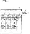
- FIG. 1 is a schematic diagram showing an example of a configuration of an imaging device to which the present invention is applied.
- the imaging device shown in the diagram includes a plurality of photosensors 1, a plurality of charge transfer portions 2, a plurality of charge-detecting circuits 3, a horizontal scanning circuit 4 which serves as scanning means, a horizontal signal line 5, and an output amplifier 6 which serves as output means.
- the plurality of photosensors 1 are disposed two-dimensionally in the form of a matrix.
- Each of photosensors 1 is equivalent to a photoelectric conversion portion which photoelectrically converts light received and is formed of a photodiode, for example.
- the positions of the photosensors 1, are represented by Pmn (P11, P12, P13, ⁇ , P21, P22, P23, ⁇ , P31, P32, P33, ⁇ ), where m rows are provided in the vertical direction and n columns are provided in the horizontal direction, respectively (both m and n are integers of one or above).
- the plurality of charge transfer portions 2 are provided with respect to respective columns of photosensors 1 in the form of line each adjacent to the photosensors 1.
- Each of charge transfer portions 2 transfers in order signal charges read out from a photosensor 1 of each row in the vertical direction (line direction), and is formed of a vertical CCD having a CCD structure, for example.
- the plurality of charge-detecting circuits 3 are provided with respect to each column (each line) of photosensors 1 in the form of a matrix, having a corresponding relation of 1:1 to the charge transfer portions 2.
- Each of the charge-detecting circuits 3 is equivalent to charge-detecting means and includes an FD (floating diffusion) amplifier and an FD reset transistor, for example.
- the charge-detecting circuit 3 is connected to one end of the charge transfer portion 2 (to the portion where vertical transfer ends). With performing voltage-conversion on signal charges read out from the corresponding charge transfer portion 2, each of the charge-detecting circuits 3 generates a signal voltage in accordance with the amount of the relevant signal charge.
- the horizontal scanning circuit 4 selects the plurality of charge-detecting circuits 3 in order in a horizontal direction to sequentially read out signal voltages generated in each of the charge-detecting circuits 3 to the horizontal signal line 5.
- the horizontal scanning circuit 4 outputs a horizontal scanning pulse in synchronization with a horizontal scanning period to the object charge-detecting circuit 3 from which a signal voltage is read out.
- the output amplifier 6 amplifies and outputs signal voltages read out to the horizontal signal line 5 by the above-described horizontal scanning circuit 4, and is connected to one end of the horizontal signal line 5.
- four of the charge-detecting circuits 3 are made to be one group and one output amplifier 6 is provided for each group, for example. In this case, the number of output amplifiers 6 is a quarter of the number of charge-detecting circuits 3.
- FIG. 2 A specific example of a configuration from the charge-detecting circuits 3 to the output amplifier 6 is shown in FIG. 2.
- four charge-detecting circuits (FD) 3 are connected to a common horizontal signal line 5 through corresponding switches 7.
- Each of switches 7 performs a switching operation (ON/OFF operation) in accordance with a horizontal scanning pulse ⁇ Hn (n is an integer of one or above) output from the horizontal scanning circuit 4.
- These switches 7 are each connected between the charge-detecting circuits 3 and the horizontal signal line 5.
- the four charge-detecting circuits 3 and the corresponding four switches 7 are termed 3A, 3B, 3C, 3D, and 7A, 7B, 7C, 7D respectively so as to be discriminated.
- a horizontal scanning pulse ⁇ Hn for horizontal scanning is output from the horizontal scanning circuit 4 to the switches 7A, 7B, 7C, 7D in order.
- the corresponding switch 7A performs a switching operation (turns ON).
- a signal voltage. is read out from the charge-detecting circuit 3A to the horizontal signal line 5, and this signal voltage is amplified in the output amplifier 6 to be output.
- FIG. 3 is a figure showing an example of a configuration for correcting the output level of a signal voltage output from an output amplifier.
- a signal processing circuit 8 to the output terminal of the output amplifier 6 is connected one input terminal of a signal processing circuit 8. Further, between the output terminal of the output amplifier 6 and the other input terminal of the signal processing circuit 8, a sample-hold circuit (hereinafter termed an S/H circuit) 9 and a memory 10 are connected in series.
- S/H circuit sample-hold circuit
- the S/H circuit 9 samples a signal voltage output from the output amplifier 6 in accordance with a sample-hold pulse ( ⁇ SH).
- the memory 10 stores as a memory voltage a signal voltage sampled in the S/H circuit 9 and is equivalent to memory means in the present invention. In this memory 10, a plurality of memory voltages are stored corresponding to timings of sampling.
- signal voltages output from the output amplifier 6 are read out in order from the plurality of charge-detecting circuits 3 to the horizontal signal line 5 by the horizontal scanning circuit 4, without the charge transfer portions 2 transferring (vertically transferring) signal charges.
- the transfer of signal charges by the charge transfer portions 2 can be controlled not to be performed by suspending the output of vertical transfer pulses to the charge transfer portions 2.
- signal voltages corresponding to the four charge-detecting circuits 3A, 3B, 3C, 3D are read out from one output amplifier 6 in order by the horizontal scanning circuit 4 in accordance with the above-described configuration shown in FIG. 2, and each signal voltage is sequentially sampled by a sample-hold pulse ⁇ SH.
- the memory 10 reads out a signal voltage held in the S/H circuit 9 to be written into a predetermined memory area. Further, the memory 10 writes a signal voltage (memory voltage) in synchronization with a sample-hold pulse ⁇ SH.
- a memory voltage Vm1 read out from the charge-detecting circuit 3A and then sampled, a memory voltage Vm2 read out from the charge-detecting circuit 3B and then sampled, a memory voltage Vm3 read out from the charge-detecting circuit 3C and then sampled, and a memory voltage Vm4 read out from the charge-detecting circuit 3D and then sampled are stored (written) separately.
- the signal processing circuit 8 executes predetermined signal processing, using signal voltages output from the output amplifier 6 and memory voltages stored in the memory 10.
- signal voltages output from the output amplifier 6 are the ones read out from the plurality of charge-detecting circuits 3 to the horizontal signal line 5 in order by the horizontal scanning circuit 4, with transferring (vertically transferring) signal charges read out from the photosensors 1 to the charge transfer portions 2.
- the signal processing circuit 8 executes arithmetic processing using signal voltages output from the output amplifier 6 and memory voltages stored in the memory 10, as one of the above-described signal processing.
- the signal processing circuit 8 corrects the level (black level in particular) of signal voltages output from the output amplifier 6, and signal voltages after this correction (hereinafter called corrected signal voltages) are output from the output terminal thereof.
- corrected signal voltages signal voltages after this correction
- the signal processing circuit 8 calculates the difference values between those signal voltages, and the difference values (arithmetic processing results) are output as corrected signal voltages.
- photosensors 1, charge transfer portions 2, charge-detecting circuits 3, horizontal scanning circuit 4,signal processing circuit 8 and memory 10 be formed on the same semiconductor chip.
- photosensors 1, charge transfer portions 2, charge-detecting circuits 3 and horizontal scanning circuit 4 it is also possible to form the photosensors 1, charge transfer portions 2, charge-detecting circuits 3 and horizontal scanning circuit 4 on the same semiconductor chip, and to form the signal processing circuit 8 and memory 10 outside the semiconductor chip.
- FIG. 4 is a block diagram showing an example of a configuration for timing control.
- a reference clock pulse generation portion 11 generates a reference clock pulse at constant intervals.
- a timing pulse generation portion 12 generates various kinds of timing pulses (timing pulses for vertical transfer, timing pulses for horizontal scanning, timing pulses for FD drive, timing pulses for S/H circuit drive, and the like), using reference clock pulse signals generated from the reference clock pulse.
- a vertical driver 13 generates a vertical transfer pulse ( ⁇ Vm) in accordance with a timing pulse for vertical transfer, which is input from the timing pulse generation portion 12, and then drives a charge transfer portion (vertical CCD) 2 using this vertical transfer pulse.
- a horizontal scanning circuit 4 generates a horizontal scanning pulse ( ⁇ Hn) in accordance with a timing pulse for horizontal scanning, which is input from the timing pulse generation portion 12, and then selectively scans each of charge-detecting circuits 3 in order using this horizontal scanning pulse.
- An FD driver 14 generates an FD reset pulse ( ⁇ RS) in accordance with a pulse for FD drive, which is input from the timing pulse generation portion 12, and then drives each of charge-detecting circuits (FD) 3 using this FD reset pulse.
- An S/H driver 15 generates a sample-hold pulse ( ⁇ SH) in accordance with a pulse for S/H drive, which is input from the timing pulse generation portion 12, and then drives an S/H circuit 9 using this sample-hold pulse.
- the FD driver 14 outputs FD reset pulses ⁇ RS at constant intervals
- the S/H driver 15 outputs sample-hold pulses ⁇ SH approximately in the middle of the interval of the FD reset pulses ⁇ RS.
- the sample-hold pulse ⁇ SH four pulses ( ⁇ SH1, ⁇ SH2, ⁇ SH3, ⁇ SH4) are output in chronological order to the above-described S/H circuit 9 shown in FIG. 3.
- the vertical driver 13 outputs no vertical transfer pulse ⁇ Vm. Therefore, the SH pulse output period T1 is a period in which a transfer (vertical transfer) of a signal charge by the charge transfer portion 2, including the readout of a signal charge from the charge transfer portion 2 to the charge-detecting circuit 3, does not take place.
- FD reset pulses ⁇ RS and horizontal scanning pulses ⁇ Hn are continuously output. Accordingly, during the SH pulse output period T1, signal voltages from each of charge-detecting circuits 3 are read out to the horizontal signal line 5 in order by the horizontal scanning circuit 4, and these readout signal voltages are amplified in the output amplifier 6 to be output, without charge transfer portions 2 transferring signal charges. On this occasion, the readout of a signal voltage from each of the charge-detecting circuits 3 to the horizontal signal line 5 is executed in accordance with a horizontal scanning pulse ⁇ Hn output from the horizontal scanning circuit 4.
- the vertical driver 13 starts outputting vertical transfer pulses ⁇ Vm ( ⁇ V1, ⁇ V2, ⁇ V3, ⁇ V4, ⁇ ).
- a signal charge read out from each photosensor 1 to a charge transfer portion 2 is transferred by the charge transfer portion 2 in synchronization with a vertical transfer pulse ⁇ Vm and is read out from the charge transfer portion 2 to the charge-detecting circuit 3.
- a signal charge read out to each of the charge-detecting circuit 3 is converted to a signal voltage in the relevant charge-detecting circuit 3 and subsequently is read out to the output amplifier 6 in order in accordance with a horizontal scanning pulse ⁇ Hn output from the horizontal scanning circuit 4.
- signal voltages read out to the output amplifier 6 are amplified by the relevant output amplifier 6 and subsequently are output from the relevant output amplifier 6.
- SH pulse output period T1 if the output waveform of signal voltages output from the output amplifier 6 is a waveform shown in the upper part of FIG. 6, signal voltages (SH signal voltages) obtained when the S/H circuit 9 samples these signal voltages using the sample-hold pulses ⁇ SH (shown in the middle part of FIG. 6) will be such a waveform as shown in the lower part of FIG. 6.
- the black level of signal voltages output from the output amplifier 6 deviates from a black level BL to be a reference (hereinafter termed a reference black level) due to dispersion in characteristics (dispersion in gain and the like) of the charge-detecting circuits 3 connected to the charge transfer portions 2 in respective column. Therefore, the level of SH signal voltages also deviates from the reference black level BL due to dispersion in characteristics of each of the charge-detecting circuits 3 (charge-detecting circuits 3A, 3B, 3C, 3D shown in FIG. 2). SH signal voltages thus obtained are stored (written) in the memory 10 for respective timings of sampling.
- the voltage value of an SH signal voltage sample-held by a sample-hold pulse ⁇ SH1 is stored in the memory 10 as a memory voltage Vm1.
- the voltage value of an SH signal voltage sample-held by a sample-hold pulse ⁇ SH2, the voltage value of an SH signal voltage sample-held by a sample-hold pulse ⁇ SH3, and the voltage value of an SH signal voltage sample-held by a sample-hold pulse ⁇ SH4 are stored sequentially in the memory 10 as a memory voltage Vm2, a memory voltage Vm3 and a memory voltage Vm4, respectively.
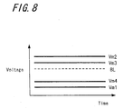
- the memory 10 are stored those four memory voltages (Vm1, Vm2, Vm3, Vm4) as shown in FIG. 8.
- the levels of the memory voltages Vm1, Vm2, Vm3, Vm4 thus stored in the memory 10 depend on dispersion in characteristics of the charge-detecting circuits 3A, 3B, 3C, 3D, irrespective of the amount of signal charges read out from the photosensors 1.
- the level of the memory voltage Vm1 depends on dispersion in characteristics of the charge-detecting circuit 3A
- the level of the memory voltage Vm2 depends on dispersion in characteristics of the charge-detecting circuit 3B
- the level of the memory voltage Vm3 depends on dispersion in characteristics of the charge-detecting circuit 3C
- the level of the memory voltage Vm4 depends on dispersion in characteristics of the charge-detecting circuit 3D.
- the memory voltages (Vm1, Vm2, Vm3, Vm4) stored in the memory 10 only include output errors (deviations from the reference black level BL) due to dispersion in characteristics of the charge-detecting circuits (3A, 3B, 3C, 3D).
- the above-described reference black level BL represents a black level of a signal voltage to be output from an output amplifier 6 when, with no signal charge stored in a photosensor 1, a signal charge is read out from the relevant photosensor 1 to be transferred by a charge transfer portion 2, and this signal charge transferred is voltage-converted in a charge-detecting circuit 3 to be read out to the relevant output amplifier 6.
- the input of readout signal voltages from the output amplifier 6 to the signal processing circuit 8 and the input of memory voltages from the memory 10 to the signal processing circuit 8 are executed in synchronization with each other. Specifically, on the input of a readout signal voltage Vr1 from the output amplifier 6 to the signal processing circuit 8, a memory voltage Vm1 is input from the memory 10 to the signal processing circuit 8 in synchronization with the input.
- a memory voltage Vm2 is input from the memory 10 to the signal processing circuit 8 in synchronization with the input; on the input of a readout signal voltage Vr3 from the output amplifier 6 to the signal processing circuit 8, a memory voltage Vm3 is input from the memory 10 to the signal processing circuit 8 in synchronization with the input;and on the input of a readout signal voltage Vr4 from the output amplifier 6 to the signal processing circuit 8, a memory voltage Vm4 is input from the memory 10 to the signal processing circuit 8 in synchronization with the input.
- the readout signal voltage Vr1 is a signal voltage read out from the charge-detecting circuit 3A and then output from the output amplifier 6, and the readout signal voltage Vr2 is a signal voltage read out from the charge-detecting circuit 3B and then output from the output amplifier 6.
- the readout signal voltage Vr3 is a signal voltage read out from the charge-detecting circuit 3C and then output from the output amplifier 6, and the readout signal voltage Vr4 is a signal voltage read out from the charge-detecting circuit 3D and then output from the output amplifier 6.
- the levels of the readout signal voltages Vr1, Vr2, Vr3, Vr4 depend on both the amount of signal charges read out from the photosensors 1 and dispersion in characteristics of the charge-detecting circuits 3A, 3B, 3C, 3D.
- arithmetic processing (signal processing) using those voltages is executed in the signal processing circuit 8.
- the arithmetic processing in the signal processing circuit 8 is executed such that the black level of readout signal voltages will correspond with the reference black level BL.
- a readout signal voltage Vr1 is input from the output amplifier 6 to the signal processing circuit 8 and a memory voltage Vm1 is input from the memory 10 to the signal processing circuit 8 in synchronization with the input
- one signal voltage for example, the readout signal voltage Vrl
- the other signal voltage for example, the memory voltage Vm1
- the difference between the voltages is calculated in the signal processing circuit 8
- the calculation result difference voltage
- the above-described arithmetic processing (signal processing) is repeatedly executed in the signal processing circuit 8 in the case where a readout signal voltage Vr2 and a memory voltage Vm2 are input, in the case where a readout signal voltage Vr3 and a memory voltage Vm3 are input, and further, in the case where a readout signal voltage Vr4 and a memory voltage Vm4 are input, respectively.
- the black level of correction signal voltages output from the signal processing circuit 8 corresponds with the reference black level BL, and readout signal levels correspond with each other, as shown in the lower part of FIG. 7.
- charge-detecting circuits 3 are made to be one group, and one output amplifier 6 is provided for each group; however, the present invention is not limited thereto, and the number of charge-detecting circuits 3 constituting one group may be more than or less than four. Further, if the number of charge-detecting circuits 3 constituting one group is four or more, output amplifiers 6 may be provided with a corresponding relation of 1:1 to charge-detecting circuits 3. Further, if the number of charge-detecting circuits 3 constituting one group is less than four, signal voltages of all the charge-detecting circuits 3 may be amplified in one common output amplifier 6 to be output.
- an imaging device can be installed in mobile phone units, PDAs (personal digital assistants) and the like.
Landscapes
- Engineering & Computer Science (AREA)
- Multimedia (AREA)
- Signal Processing (AREA)
- Solid State Image Pick-Up Elements (AREA)
- Transforming Light Signals Into Electric Signals (AREA)
Abstract
A configuration of an imaging device includes: an S/H circuit (9) which samples signal voltages read out from a plurality of charge-detecting circuits by a horizontal scanning circuit and output from an output amplifier (6), without the transfer of signal charges by a charge transfer portion; a memory 10 which stores signal voltages sampled by the S/H circuit (9) as memory voltages (Vm1 to Vm4); and a signal processing circuit (8) which executes predetermined signal processing, using signal voltages read out from the plurality of charge-detecting circuits by the horizontal scanning circuit and output from the output amplifier (6) and memory signals stored in the memory (10), with the transfer of signal charges read out from the photoelectric conversion portion to the charge transfer portion. <IMAGE>
Description
The present invention relates to an imaging device which
has a photoelectric conversion portion and a charge transfer
portion, and to a drive method of an imaging device.
As an imaging device, one in which signal charges read out
from a plurality of photoelectric conversion portions arranged
two-dimensionally in the form of a matrix are transferred in the
vertical direction by means of a charge transfer portion, and
after those signal charges are transferred in the horizontal
direction, each signal charge is voltage-converted by a common
charge-detecting means to be output is widely known.
Further, in recent years, an imaging device provided with a
plurality of charge-detecting means which perform voltage-conversion
on signal charges transferred in the vertical
direction has been proposed as the one which enables an imaging
device to be driven at high speed and so on (for example, Patent
Literature 1). In this imaging device, signal charges
transferred in the vertical direction by means of a vertical CCD
(Charge Coupled Device) are voltage-converted by the charge-detecting
means; signal voltages thus generated by the charge-detecting
means are scanned and read out in order by scanning
means; and these signal voltages read out are amplified by an
output amplifier to be output.
Published Japanese Patent Application No. 2002-135656
(claim 1, FIG. 1)
However, in the imaging device described in the above
Patent Literature 1, since a plurality of charge-detecting means
are provided, output errors occur in signal voltages due to
dispersion in characteristics (particularly dispersion in gain)
of each charge-detecting means and the signal voltages are read
out with these output errors included. Therefore, even if
exactly the same amount of signal charge is read out from each
of photoelectric conversion means, there will be dispersion
(level difference) with respect to output signal voltages
finally obtained. As a result, noise in the form of stripes
(vertical stripes or the like) may be generated in an output
image.
In order to cope with the above, characteristics of each
charge-detecting means may be adjusted separately to be the
reference level at the time when signal voltages are output;
however, as the number of charge-detecting means provided in one
imaging device increases, processes required for the adjustment
increase. Thus, in the current situation where a large number
of charge-detecting means are used, procedures to be employed
become extremely difficult in practice.
The present invention is made to solve the above-described
problems, and is to provide an imaging device and a drive method
of an imaging device, in which when a plurality of charge-detecting
means are provided, output errors due to dispersion in
characteristics of those charge-detecting means can
appropriately be corrected.
An imaging device according to the present invention
includes: a photoelectric conversion portion which
photoelectrically converts light received; a charge transfer
portion which transfers signal charges read out from the
photoelectric conversion portion; a plurality of charge-detecting
means which perform voltage-conversion on signal
charges from the charge transfer portion; scanning means which
read out signals voltage-converted by the plurality of charge-detecting
means; output means which output signals read out by
the scanning means; memory means which, without the transfer of
signal charges by the charge transfer portion, store signals
read out from the plurality of charge-detecting means by the
scanning means and output from the output means; and signal
processing means which, with the transfer of signal charges read
out from the photoelectric conversion portions to the charge
portions, execute predetermined signal processing using signals
read out from the plurality of charge-detecting means by the
scanning means and output by the output means and signals stored
in the memory means.
In this imaging device, the level of signals read out from
the plurality of charge-detecting means by the scanning means
and output by the output means, without the charge transfer
portions transferring signal charges, depends on dispersion in
characteristics of those charge-detecting means, irrespective of
the amount of signal charges read out from the photoelectric
conversion portions. Therefore, signals to be stored in the
memory means only include output errors due to dispersion in
characteristics of those charge-detecting means. On the other
hand, the level of signals read out from the plurality of
charge-detecting means by the scanning means and output by the
output means, with transferring signal charges read out from the
photoelectric conversion portions to the charge transfer
portions, depends on the amount of signal charges read out from
the photoelectric conversion portion and on dispersion in
characteristics of those charge-detecting means. Therefore, by
executing predetermined signal processing by the signal
processing means,using signals read out from the plurality of
charge-detecting means by the scanning means and output by the
output means and signals stored in the memory means, with
transferring signal charges read out from the photoelectric
conversion portion to the charge transfer portion, output error
elements due to dispersion in characteristics of respective
charge-detecting circuits can be removed from signal components
output from the output means with signal charges being read out
from the photoelectric conversion portions and with the charge
transfer portions transferring signal charges.
A drive method of an imaging device according to the
present invention is a drive method of an imaging device having
a photoelectric conversion portion which photoelectrically
converts light received, a charge transfer portion which
transfers signal charges read out from the photoelectric
conversion portion, a plurality of charge-detecting means which
perform voltage-conversion on signal charges from the charge
transfer portion, scanning means which read out signals voltage-converted
by these plurality of charge-detecting means, and
output means which output signals read out by this scanning
means, including the processes of: storing signals read out from
the plurality of charge-detecting means by the scanning means
and output from the output means without the transfer of signal
charges by the charge transfer portions; and executing
predetermined signal processing, using signals read out from the
plurality of charge-detecting means by the scanning means and
output from the output means and signals stored in the storing
process with the transfer of signal charges read out from the
photoelectric conversion portions to the charge transfer
portions.
In this drive method of an imaging device, the level of
signals read out from the plurality of charge-detecting means by
the scanning means and output from the output means, without the
charge transfer portions transferring signal charges, depends on
dispersion in characteristics of those charge-detecting means,
irrespective of the amount of signal charges read out from the
photoelectric conversion portions. Therefore, signals to be
stored in the memory process only include output errors due to
dispersion in characteristics of those charge-detecting means.
On the other hand, the level of signals read out from the
plurality of charge-detecting means by the scanning means and
output from the output means, with transferring signal charges
read out from the photoelectric conversion portion to the charge
transfer portion, depends on the amount of signal charges read
out from the photoelectric conversion portions and on dispersion
in characteristics of those charge-detecting means. Accordingly,
by executing predetermined signal processing in the signal
processing process, using signals read out from the plurality of
charge-detecting means by the scanning means and output from the
output means and signals stored in the memory process, with
transferring signal charges read out from the photoelectric
conversion portion to the charge transfer portions, output error
components due to dispersion in characteristics of respective
charge-detecting circuits can be removed from signal components
output by the output means with signal charges being read out
from the photoelectric conversion portions and with the charge
transfer portions transferring signal charges.
Hereinafter, an embodiment of the present invention is
explained in detail when applied to an imaging device which
employs an interline type transfer method, referring to the
drawings; however, the present invention can also be applied to
an imaging device which employs a frame transfer type transfer
method.
FIG. 1 is a schematic diagram showing an example of a
configuration of an imaging device to which the present
invention is applied. The imaging device shown in the diagram
includes a plurality of photosensors 1, a plurality of charge
transfer portions 2, a plurality of charge-detecting circuits 3,
a horizontal scanning circuit 4 which serves as scanning means,
a horizontal signal line 5, and an output amplifier 6 which
serves as output means.
The plurality of photosensors 1 are disposed two-dimensionally
in the form of a matrix. Each of photosensors 1
is equivalent to a photoelectric conversion portion which
photoelectrically converts light received and is formed of a
photodiode, for example. In FIG. 1, the positions of the
photosensors 1, are represented by Pmn (P11, P12, P13, ···, P21,
P22, P23, ···, P31, P32, P33, ···), where m rows are provided in
the vertical direction and n columns are provided in the
horizontal direction, respectively (both m and n are integers of
one or above).
The plurality of charge transfer portions 2 are provided
with respect to respective columns of photosensors 1 in the form
of line each adjacent to the photosensors 1. Each of charge
transfer portions 2 transfers in order signal charges read out
from a photosensor 1 of each row in the vertical direction (line
direction), and is formed of a vertical CCD having a CCD
structure, for example.
The plurality of charge-detecting circuits 3 are provided
with respect to each column (each line) of photosensors 1 in the
form of a matrix, having a corresponding relation of 1:1 to the
charge transfer portions 2. Each of the charge-detecting
circuits 3 is equivalent to charge-detecting means and includes
an FD (floating diffusion) amplifier and an FD reset transistor,
for example. The charge-detecting circuit 3 is connected to one
end of the charge transfer portion 2 (to the portion where
vertical transfer ends). With performing voltage-conversion on
signal charges read out from the corresponding charge transfer
portion 2, each of the charge-detecting circuits 3 generates a
signal voltage in accordance with the amount of the relevant
signal charge.
The horizontal scanning circuit 4 selects the plurality of
charge-detecting circuits 3 in order in a horizontal direction
to sequentially read out signal voltages generated in each of
the charge-detecting circuits 3 to the horizontal signal line 5.
When reading out signal voltages from the charge-detecting
circuits 3 to the horizontal signal line 5, the horizontal
scanning circuit 4 outputs a horizontal scanning pulse in
synchronization with a horizontal scanning period to the object
charge-detecting circuit 3 from which a signal voltage is read
out.
The output amplifier 6 amplifies and outputs signal
voltages read out to the horizontal signal line 5 by the above-described
horizontal scanning circuit 4, and is connected to one
end of the horizontal signal line 5. Regarding this output
amplifier 6, four of the charge-detecting circuits 3 are made to
be one group and one output amplifier 6 is provided for each
group, for example. In this case, the number of output
amplifiers 6 is a quarter of the number of charge-detecting
circuits 3.
A specific example of a configuration from the charge-detecting
circuits 3 to the output amplifier 6 is shown in FIG.
2. As shown in the figure, four charge-detecting circuits (FD)
3 are connected to a common horizontal signal line 5 through
corresponding switches 7. Each of switches 7 performs a
switching operation (ON/OFF operation) in accordance with a
horizontal scanning pulse ϕHn (n is an integer of one or above)
output from the horizontal scanning circuit 4. These switches 7
are each connected between the charge-detecting circuits 3 and
the horizontal signal line 5. Note that in the following
explanations, the four charge-detecting circuits 3 and the
corresponding four switches 7 are termed 3A, 3B, 3C, 3D, and 7A,
7B, 7C, 7D respectively so as to be discriminated.
In the above-described configuration shown in FIG. 2, a
horizontal scanning pulse ϕHn for horizontal scanning is output
from the horizontal scanning circuit 4 to the switches 7A, 7B,
7C, 7D in order. On this occasion, when a horizontal scanning
pulse ϕH1 is output from the horizontal scanning circuit 4, the
corresponding switch 7A performs a switching operation (turns
ON). Thus, a signal voltage.is read out from the charge-detecting
circuit 3A to the horizontal signal line 5, and this
signal voltage is amplified in the output amplifier 6 to be
output.
Similarly, when a horizontal scanning pulse ϕH2 is output
from the horizontal scanning circuit 4, the corresponding switch
7B performs a switching operation (turns ON); thus, a signal
voltage is read out from the charge-detecting circuit 3B to the
horizontal signal line 5, and this signal voltage is amplified
in the output amplifier 6 to be output. Further, when a
horizontal scanning pulse ϕH3 is output from the horizontal
scanning circuit 4, the corresponding switch 7C performs a
switching operation (turns ON); thus, a signal voltage is read
out from the charge-detecting circuit 3C to the horizontal
signal line 5, and this signal voltage is amplified in the
output amplifier 6 to be output. Further, when a horizontal
scanning pulse ϕH4 is output from the horizontal scanning
circuit 4, the corresponding switch 7D performs a switching
operation (turns ON); thus, a signal voltage is read out from
the charge-detecting circuit 3D to the horizontal signal line 5,
and this signal voltage is amplified in the output amplifier 6
to be output.
FIG. 3 is a figure showing an example of a configuration
for correcting the output level of a signal voltage output from
an output amplifier. In FIG. 3, to the output terminal of the
output amplifier 6 is connected one input terminal of a signal
processing circuit 8. Further, between the output terminal of
the output amplifier 6 and the other input terminal of the
signal processing circuit 8, a sample-hold circuit (hereinafter
termed an S/H circuit) 9 and a memory 10 are connected in series.
The S/H circuit 9 samples a signal voltage output from the
output amplifier 6 in accordance with a sample-hold pulse (ϕSH).
The memory 10 stores as a memory voltage a signal voltage
sampled in the S/H circuit 9 and is equivalent to memory means
in the present invention. In this memory 10, a plurality of
memory voltages are stored corresponding to timings of sampling.
On storing memory voltages in the memory 10, signal voltages
output from the output amplifier 6 are read out in order from
the plurality of charge-detecting circuits 3 to the horizontal
signal line 5 by the horizontal scanning circuit 4, without the
charge transfer portions 2 transferring (vertically
transferring) signal charges. Hereupon, the transfer of signal
charges by the charge transfer portions 2 can be controlled not
to be performed by suspending the output of vertical transfer
pulses to the charge transfer portions 2.
Here, signal voltages corresponding to the four charge-detecting
circuits 3A, 3B, 3C, 3D are read out from one output
amplifier 6 in order by the horizontal scanning circuit 4 in
accordance with the above-described configuration shown in FIG.
2, and each signal voltage is sequentially sampled by a sample-hold
pulse ϕSH. Correspondingly, after a predetermined period
of time started from a rise of a sample-hold pulse ϕSH has
passed (before the next sample-hold pulse ϕSH rises), the memory
10 reads out a signal voltage held in the S/H circuit 9 to be
written into a predetermined memory area. Further, the memory
10 writes a signal voltage (memory voltage) in synchronization
with a sample-hold pulse ϕSH. Therefore, in the memory 10, a
memory voltage Vm1 read out from the charge-detecting circuit 3A
and then sampled, a memory voltage Vm2 read out from the charge-detecting
circuit 3B and then sampled, a memory voltage Vm3 read
out from the charge-detecting circuit 3C and then sampled, and a
memory voltage Vm4 read out from the charge-detecting circuit 3D
and then sampled are stored (written) separately.
The signal processing circuit 8 executes predetermined
signal processing, using signal voltages output from the output
amplifier 6 and memory voltages stored in the memory 10. In
this case, signal voltages output from the output amplifier 6
are the ones read out from the plurality of charge-detecting
circuits 3 to the horizontal signal line 5 in order by the
horizontal scanning circuit 4, with transferring (vertically
transferring) signal charges read out from the photosensors 1 to
the charge transfer portions 2.
The signal processing circuit 8 executes arithmetic
processing using signal voltages output from the output
amplifier 6 and memory voltages stored in the memory 10, as one
of the above-described signal processing. In this arithmetic
processing, the signal processing circuit 8 corrects the level
(black level in particular) of signal voltages output from the
output amplifier 6, and signal voltages after this correction
(hereinafter called corrected signal voltages) are output from
the output terminal thereof. Specifically, by means of
arithmetic processing using signal voltages output from the
output amplifier 6 and memory voltages (Vm1, Vm2, Vm3, Vm4) read
out from the memory 10, the signal processing circuit 8
calculates the difference values between those signal voltages,
and the difference values (arithmetic processing results) are
output as corrected signal voltages.
Further, it is desirable that the above-described
photosensors 1, charge transfer portions 2, charge-detecting
circuits 3, horizontal scanning circuit 4,signal processing
circuit 8 and memory 10 be formed on the same semiconductor chip.
However, it is also possible to form the photosensors 1, charge
transfer portions 2, charge-detecting circuits 3 and horizontal
scanning circuit 4 on the same semiconductor chip, and to form
the signal processing circuit 8 and memory 10 outside the
semiconductor chip.
FIG. 4 is a block diagram showing an example of a
configuration for timing control. In FIG. 4, a reference clock
pulse generation portion 11 generates a reference clock pulse at
constant intervals. A timing pulse generation portion 12
generates various kinds of timing pulses (timing pulses for
vertical transfer, timing pulses for horizontal scanning, timing
pulses for FD drive, timing pulses for S/H circuit drive, and
the like), using reference clock pulse signals generated from
the reference clock pulse.
A vertical driver 13 generates a vertical transfer pulse
(ϕVm) in accordance with a timing pulse for vertical transfer,
which is input from the timing pulse generation portion 12, and
then drives a charge transfer portion (vertical CCD) 2 using
this vertical transfer pulse. A horizontal scanning circuit 4
generates a horizontal scanning pulse (ϕHn) in accordance with a
timing pulse for horizontal scanning, which is input from the
timing pulse generation portion 12, and then selectively scans
each of charge-detecting circuits 3 in order using this
horizontal scanning pulse.
An FD driver 14 generates an FD reset pulse (ϕRS) in
accordance with a pulse for FD drive, which is input from the
timing pulse generation portion 12, and then drives each of
charge-detecting circuits (FD) 3 using this FD reset pulse. An
S/H driver 15 generates a sample-hold pulse (ϕSH) in accordance
with a pulse for S/H drive, which is input from the timing pulse
generation portion 12, and then drives an S/H circuit 9 using
this sample-hold pulse.
Next, operations of an imaging device, based on various
kinds of timing pulses generated in the timing pulse generation
portion 12 are explained, referring to the timing charts of FIGS.
5 to 7.
First, in FIG. 5, the FD driver 14 outputs FD reset pulses
ϕRS at constant intervals, and the S/H driver 15 outputs sample-hold
pulses ϕSH approximately in the middle of the interval of
the FD reset pulses ϕRS. Regarding the sample-hold pulse ϕSH,
four pulses (ϕSH1, ϕSH2, ϕSH3, ϕSH4) are output in chronological
order to the above-described S/H circuit 9 shown in FIG. 3.
During a period in which the sample-hold pulses ϕSH are output
(hereinafter called an SH pulse output period) T1, the vertical
driver 13 outputs no vertical transfer pulse ϕVm. Therefore,
the SH pulse output period T1 is a period in which a transfer
(vertical transfer) of a signal charge by the charge transfer
portion 2, including the readout of a signal charge from the
charge transfer portion 2 to the charge-detecting circuit 3,
does not take place.
However, during the SH pulse output period T1, FD reset
pulses ϕRS and horizontal scanning pulses ϕHn are continuously
output. Accordingly, during the SH pulse output period T1,
signal voltages from each of charge-detecting circuits 3 are
read out to the horizontal signal line 5 in order by the
horizontal scanning circuit 4, and these readout signal voltages
are amplified in the output amplifier 6 to be output, without
charge transfer portions 2 transferring signal charges. On this
occasion, the readout of a signal voltage from each of the
charge-detecting circuits 3 to the horizontal signal line 5 is
executed in accordance with a horizontal scanning pulse ϕHn
output from the horizontal scanning circuit 4.
After that, when the output of the sample-hold pulses ϕSH
by the S/H driver 15 is completed, the vertical driver 13 starts
outputting vertical transfer pulses ϕVm (ϕV1, ϕV2, ϕV3, ϕV4,
··· ). Thus, a signal charge read out from each photosensor 1 to
a charge transfer portion 2 is transferred by the charge
transfer portion 2 in synchronization with a vertical transfer
pulse ϕVm and is read out from the charge transfer portion 2 to
the charge-detecting circuit 3. Further, a signal charge read
out to each of the charge-detecting circuit 3 is converted to a
signal voltage in the relevant charge-detecting circuit 3 and
subsequently is read out to the output amplifier 6 in order in
accordance with a horizontal scanning pulse ϕHn output from the
horizontal scanning circuit 4. Therefore, during a period in
which vertical transfer pulses ϕVm are output, with transferring
(vertically transferring) signal charges read out from the
photosensors 1 to the charge transfer portions 2, signal
voltages from each of the charge-detecting circuits 3 are read
out to the horizontal signal line 5 in order by the horizontal
scanning circuit 4, and the signal voltages read out are
amplified in the output amplifier 6 to be output. In this case,
if the charge transfer portion 2 includes a CCD structure, the
transfer of signal charges by the charge transfer portions 2 is
signal charge transfer performed by CCDs. Further, the readout
of a signal voltage from each of the charge-detecting circuits 3
to the horizontal signal line 5 is executed in accordance with a
horizontal scanning pulse ϕHn output from the horizontal
scanning circuit 4.
On the other hand, signal voltages read out to the output
amplifier 6 are amplified by the relevant output amplifier 6 and
subsequently are output from the relevant output amplifier 6.
Here, in the above-described SH pulse output period T1, if the
output waveform of signal voltages output from the output
amplifier 6 is a waveform shown in the upper part of FIG. 6,
signal voltages (SH signal voltages) obtained when the S/H
circuit 9 samples these signal voltages using the sample-hold
pulses ϕSH (shown in the middle part of FIG. 6) will be such a
waveform as shown in the lower part of FIG. 6.
Specifically, the black level of signal voltages output
from the output amplifier 6 deviates from a black level BL to be
a reference (hereinafter termed a reference black level) due to
dispersion in characteristics (dispersion in gain and the like)
of the charge-detecting circuits 3 connected to the charge
transfer portions 2 in respective column. Therefore, the level
of SH signal voltages also deviates from the reference black
level BL due to dispersion in characteristics of each of the
charge-detecting circuits 3 (charge-detecting circuits 3A, 3B,
3C, 3D shown in FIG. 2). SH signal voltages thus obtained are
stored (written) in the memory 10 for respective timings of
sampling.
Specifically, the voltage value of an SH signal voltage
sample-held by a sample-hold pulse ϕSH1 is stored in the memory
10 as a memory voltage Vm1. Similarly, the voltage value of an
SH signal voltage sample-held by a sample-hold pulse ϕSH2, the
voltage value of an SH signal voltage sample-held by a sample-hold
pulse ϕSH3, and the voltage value of an SH signal voltage
sample-held by a sample-hold pulse ϕSH4 are stored sequentially
in the memory 10 as a memory voltage Vm2, a memory voltage Vm3
and a memory voltage Vm4, respectively.
Thus, in the memory 10 are stored those four memory
voltages (Vm1, Vm2, Vm3, Vm4) as shown in FIG. 8. The levels of
the memory voltages Vm1, Vm2, Vm3, Vm4 thus stored in the memory
10 depend on dispersion in characteristics of the charge-detecting
circuits 3A, 3B, 3C, 3D, irrespective of the amount of
signal charges read out from the photosensors 1. Specifically,
the level of the memory voltage Vm1 depends on dispersion in
characteristics of the charge-detecting circuit 3A, the level of
the memory voltage Vm2 depends on dispersion in characteristics
of the charge-detecting circuit 3B, the level of the memory
voltage Vm3 depends on dispersion in characteristics of the
charge-detecting circuit 3C, and the level of the memory voltage
Vm4 depends on dispersion in characteristics of the charge-detecting
circuit 3D. Accordingly, the memory voltages (Vm1,
Vm2, Vm3, Vm4) stored in the memory 10 only include output
errors (deviations from the reference black level BL) due to
dispersion in characteristics of the charge-detecting circuits
(3A, 3B, 3C, 3D).
Note that, the above-described reference black level BL
represents a black level of a signal voltage to be output from
an output amplifier 6 when, with no signal charge stored in a
photosensor 1, a signal charge is read out from the relevant
photosensor 1 to be transferred by a charge transfer portion 2,
and this signal charge transferred is voltage-converted in a
charge-detecting circuit 3 to be read out to the relevant output
amplifier 6.
On the other hand, after starting the output of vertical
transfer pulses ϕVm (in other words, after starting the transfer
of signal charges by the charge transfer portions 2), if signal
voltages read out from each of the charge-detecting circuits 3
in order and then output from the output amplifier 6
(hereinafter termed readout signal voltages) are, for example,
the one shown in the upper part of FIG. 7, these readout signal
voltages are input to one input terminal of a signal processing
circuit 8. Hereupon, the level of readout signal voltages
output from the output amplifier 6 are shown assuming that all
the amount of signal charges read out from the photosensors 1 is
the same. On this occasion, to the other input terminal of the
signal processing circuit 8 are input memory voltages read out
from the memory 10 concurrently with the input of readout signal
voltages to the relevant signal processing circuit 8.
The input of readout signal voltages from the output
amplifier 6 to the signal processing circuit 8 and the input of
memory voltages from the memory 10 to the signal processing
circuit 8 are executed in synchronization with each other.
Specifically, on the input of a readout signal voltage Vr1 from
the output amplifier 6 to the signal processing circuit 8, a
memory voltage Vm1 is input from the memory 10 to the signal
processing circuit 8 in synchronization with the input.
Similarly, on the input of a readout signal voltage Vr2 from the
output amplifier 6 to the signal processing circuit 8, a memory
voltage Vm2 is input from the memory 10 to the signal processing
circuit 8 in synchronization with the input; on the input of a
readout signal voltage Vr3 from the output amplifier 6 to the
signal processing circuit 8, a memory voltage Vm3 is input from
the memory 10 to the signal processing circuit 8 in
synchronization with the input;and on the input of a readout
signal voltage Vr4 from the output amplifier 6 to the signal
processing circuit 8, a memory voltage Vm4 is input from the
memory 10 to the signal processing circuit 8 in synchronization
with the input.
Among these, the readout signal voltage Vr1 is a signal
voltage read out from the charge-detecting circuit 3A and then
output from the output amplifier 6, and the readout signal
voltage Vr2 is a signal voltage read out from the charge-detecting
circuit 3B and then output from the output amplifier 6.
Further, the readout signal voltage Vr3 is a signal voltage read
out from the charge-detecting circuit 3C and then output from
the output amplifier 6, and the readout signal voltage Vr4 is a
signal voltage read out from the charge-detecting circuit 3D and
then output from the output amplifier 6. The levels of the
readout signal voltages Vr1, Vr2, Vr3, Vr4 depend on both the
amount of signal charges read out from the photosensors 1 and
dispersion in characteristics of the charge-detecting circuits
3A, 3B, 3C, 3D.
On the input of a readout signal voltage and a memory
voltage in this manner, arithmetic processing (signal
processing) using those voltages is executed in the signal
processing circuit 8. The arithmetic processing in the signal
processing circuit 8 is executed such that the black level of
readout signal voltages will correspond with the reference black
level BL. Specifically, for example, if a readout signal
voltage Vr1 is input from the output amplifier 6 to the signal
processing circuit 8, and a memory voltage Vm1 is input from the
memory 10 to the signal processing circuit 8 in synchronization
with the input, one signal voltage (for example, the readout
signal voltage Vrl) is made a positive voltage while the other
signal voltage (for example, the memory voltage Vm1) is made a
negative voltage, the difference between the voltages is
calculated in the signal processing circuit 8, and the
calculation result (difference voltage) is output as a corrected
signal voltage. Thus, from signal components output from the
output amplifier 6 as a result of the readout of signal charges
from the photosensors 1 and the transfer of signal charges by
the charge transfer portions 2, output error components due to
dispersion in characteristics of the charge-detecting circuits
3A, 3B, 3C, 3D can be removed and then output.
The above-described arithmetic processing (signal
processing) is repeatedly executed in the signal processing
circuit 8 in the case where a readout signal voltage Vr2 and a
memory voltage Vm2 are input, in the case where a readout signal
voltage Vr3 and a memory voltage Vm3 are input, and further, in
the case where a readout signal voltage Vr4 and a memory voltage
Vm4 are input, respectively. Thus, as described above, if all
the amount of signal charges read out from the photosensors 1 is
the same, the black level of correction signal voltages output
from the signal processing circuit 8 corresponds with the
reference black level BL, and readout signal levels correspond
with each other, as shown in the lower part of FIG. 7.
Therefore, if there is dispersion in characteristics of the
charge-detecting circuits 3, output errors caused by the
dispersion in characteristics can be corrected appropriately.
Further, if there is dispersion in characteristics of each of
the output amplifiers 6, output errors caused by the dispersion
in characteristics can be corrected in an appropriate manner.
Further, other than the charge-detecting circuits 3 and the
output amplifier 6, if there is dispersion in characteristics of
the circuit part (wiring and the like) from the charge-detecting
circuits 3 to the output amplifier 6, output errors caused by
the dispersion in characteristics can be corrected in an
appropriate manner. As a result, noise in a stripe pattern can
be reliably prevented from occurring in an output image.
It should be noted that in the above-described embodiment,
four charge-detecting circuits 3 are made to be one group, and
one output amplifier 6 is provided for each group; however, the
present invention is not limited thereto, and the number of
charge-detecting circuits 3 constituting one group may be more
than or less than four. Further, if the number of charge-detecting
circuits 3 constituting one group is four or more,
output amplifiers 6 may be provided with a corresponding
relation of 1:1 to charge-detecting circuits 3. Further, if the
number of charge-detecting circuits 3 constituting one group is
less than four, signal voltages of all the charge-detecting
circuits 3 may be amplified in one common output amplifier 6 to
be output.
Further, an imaging device according to the present
invention can be installed in mobile phone units, PDAs (personal
digital assistants) and the like.
- 1
- PHOTOSENSOR
- 2
- CHARGE TRANSFER PORTION
- 3
- CHARGE-DETECTING CIRCUIT
- 4 .
- HORIZONTAL SCANNING CIRCUIT
- 5
- HORIZONTAL SIGNAL LINE
- 6
- OUTPUT AMPLIFIER
- 7
- SWITCH
- 8
- SIGNAL PROCESSING CIRCUIT
- 9
- S/H CIRCUIT
- 10
- MEMORY
Claims (13)
- An imaging device comprising:a photoelectric conversion portion which photoelectrically converts light received;a charge transfer portion which transfers signal charges read out from said photoelectric conversion portion;a plurality of charge-detecting means which perform voltage-conversion on signal charges from said charge transfer portion;scanning means which read out signals voltage-converted by said plurality of charge-detecting means;output means which output signals read out by said scanning means;memory means which, without the transfer of signal charges by said charge transfer portion, store signals read out from said plurality of charge-detecting means by said scanning means and output from said output means; andsignal processing means which, with the transfer of signal charges read out from said photoelectric conversion portion to said charge transfer portion, execute predetermined signal processing using signals read out from said plurality of charge-detecting means by said scanning means and output from said output means and signals stored in said memory means.
- An imaging device according to claim 1,
wherein said photoelectric conversion portion, said charge transfer portion, said charge-detecting means, said scanning means, said memory means and said signal processing means are formed on the same semiconductor chip. - An imaging device according to claim 1,
wherein said photoelectric conversion portion, said charge transfer portion, said charge-detecting means and said scanning means are formed on the same semiconductor chip, and said memory means and said signal processing means are formed outside said semiconductor chip. - An imaging device according to claim 1,
wherein said charge transfer portion includes a CCD structure. - An imaging device according to claim 1,
wherein said signal processing means executes, as said predetermined signal processing, arithmetic processing using signals read out from said plurality of charge-detecting means by said scanning means and output from said output means and signals stored in said memory means. - An imaging device according to claim 5,
wherein said signal processing means calculates the difference value of signals by means of said arithmetic processing, and the difference value is output as a corrected signal. - An imaging device according to claim 1,
wherein said scanning means read out in order said signals voltage-converted. - An imaging device according to claim 1, further comprising a sample-hold circuit between said output means and said memory means.
- A drive method of an imaging device including a photoelectric conversion portion which photoelectrically converts light received, a charge transfer portion which transfers signal charges read out from said photoelectric conversion portion, a plurality of charge-detecting means which perform voltage-conversion on signal charges from said charge transfer portions, scanning means which read out signals voltage-converted by said plurality of charge-detecting means, and output means which output signals read out by said scanning means, comprising the steps of:storing signals read out from said plurality of charge-detecting means by said scanning means and output from said output means, without the transfer of signal charges by said charge transfer portion; andexecuting predetermined signal processing, using signals read out from said plurality of charge-detecting means by said scanning means and output from said output means and signals stored in said memory means, with the transfer of signal charges read out from said photoelectric conversion portion to said charge transfer portion.
- A drive method of an imaging device according to claim 9,
wherein the transfer of signal charges by said charge transfer portion is charge transfer by a CCD. - A drive method of an imaging device according to claim 9,
wherein in said signal processing step, arithmetic processing is executed as said predetermined signal processing. - A drive method of an imaging device according to claim 11,
wherein in said signal processing step, the difference value of signals is calculated by means of said arithmetic processing, and the difference value is output as a corrected signal. - A drive method of an imaging device according to claim 9,
wherein said scanning means read out in order said signals voltage-converted.
Applications Claiming Priority (3)
| Application Number | Priority Date | Filing Date | Title |
|---|---|---|---|
| JP2003039102 | 2003-02-18 | ||
| JP2003039102A JP2004266363A (en) | 2003-02-18 | 2003-02-18 | Imaging apparatus and driving method of imaging apparatus |
| PCT/JP2004/001287 WO2004075539A1 (en) | 2003-02-18 | 2004-02-06 | Imaging device and method for driving imaging device |
Publications (1)
| Publication Number | Publication Date |
|---|---|
| EP1603331A1 true EP1603331A1 (en) | 2005-12-07 |
Family
ID=32905157
Family Applications (1)
| Application Number | Title | Priority Date | Filing Date |
|---|---|---|---|
| EP04708864A Withdrawn EP1603331A1 (en) | 2003-02-18 | 2004-02-06 | Imaging device and method for driving imaging device |
Country Status (7)
| Country | Link |
|---|---|
| US (1) | US20060146162A1 (en) |
| EP (1) | EP1603331A1 (en) |
| JP (1) | JP2004266363A (en) |
| KR (1) | KR20050099618A (en) |
| CN (1) | CN1751502A (en) |
| TW (1) | TWI289925B (en) |
| WO (1) | WO2004075539A1 (en) |
Families Citing this family (2)
| Publication number | Priority date | Publication date | Assignee | Title |
|---|---|---|---|---|
| US8557950B2 (en) | 2005-06-16 | 2013-10-15 | Grupo Petrotemex, S.A. De C.V. | High intrinsic viscosity melt phase polyester polymers with acceptable acetaldehyde generation rates |
| JP5282543B2 (en) * | 2008-11-28 | 2013-09-04 | ソニー株式会社 | Solid-state imaging device, driving method of solid-state imaging device, and imaging device |
Family Cites Families (14)
| Publication number | Priority date | Publication date | Assignee | Title |
|---|---|---|---|---|
| US4907089A (en) * | 1988-01-14 | 1990-03-06 | Sony Corp. | Timing pulse generator |
| JPH0287784A (en) * | 1988-09-26 | 1990-03-28 | Canon Inc | Original reading device |
| US5355164A (en) * | 1990-06-25 | 1994-10-11 | Fuji Photo Film Co., Ltd. | Method and apparatus of correction image read signals by removing the influence of dark current therefrom |
| JPH04365274A (en) * | 1991-06-13 | 1992-12-17 | Toshiba Corp | Solid-state image pickup device |
| US5943094A (en) * | 1991-09-04 | 1999-08-24 | Canon Kabushiki Kaisha | Image pickup device with noise data generation |
| US5572155A (en) * | 1994-06-20 | 1996-11-05 | Fuji Photo Film Co., Ltd. | CCD signal read-out circuit free from ailiasing of high-frequency noises |
| KR100220863B1 (en) * | 1995-11-30 | 1999-09-15 | 무네유키 가코우 | The signal reading device of the solid- |
| GB2317522B (en) * | 1996-09-12 | 2000-09-27 | Vsli Vision Limited | Low noise operation of an image sensor |
| JPH11155103A (en) * | 1997-11-21 | 1999-06-08 | Toshiba Corp | Solid-state imaging device |
| US20020176009A1 (en) * | 1998-05-08 | 2002-11-28 | Johnson Sandra Marie | Image processor circuits, systems, and methods |
| JP3792956B2 (en) * | 1999-08-19 | 2006-07-05 | キヤノン株式会社 | Image input device and image input system using the same |
| JP3937716B2 (en) * | 2000-10-24 | 2007-06-27 | キヤノン株式会社 | Solid-state imaging device and imaging system |
| US7050098B2 (en) * | 2001-03-29 | 2006-05-23 | Canon Kabushiki Kaisha | Signal processing apparatus and method, and image sensing apparatus having a plurality of image sensing regions per image frame |
| JP3697172B2 (en) * | 2001-03-29 | 2005-09-21 | キヤノン株式会社 | Signal processing apparatus, signal processing method, and imaging apparatus |
-
2003
- 2003-02-18 JP JP2003039102A patent/JP2004266363A/en active Pending
-
2004
- 2004-02-06 US US10/544,732 patent/US20060146162A1/en not_active Abandoned
- 2004-02-06 EP EP04708864A patent/EP1603331A1/en not_active Withdrawn
- 2004-02-06 CN CNA2004800045064A patent/CN1751502A/en active Pending
- 2004-02-06 WO PCT/JP2004/001287 patent/WO2004075539A1/en not_active Ceased
- 2004-02-06 KR KR1020057014689A patent/KR20050099618A/en not_active Ceased
- 2004-02-18 TW TW093103925A patent/TWI289925B/en not_active IP Right Cessation
Non-Patent Citations (1)
| Title |
|---|
| See references of WO2004075539A1 * |
Also Published As
| Publication number | Publication date |
|---|---|
| KR20050099618A (en) | 2005-10-14 |
| TW200427075A (en) | 2004-12-01 |
| CN1751502A (en) | 2006-03-22 |
| US20060146162A1 (en) | 2006-07-06 |
| JP2004266363A (en) | 2004-09-24 |
| WO2004075539A1 (en) | 2004-09-02 |
| TWI289925B (en) | 2007-11-11 |
Similar Documents
| Publication | Publication Date | Title |
|---|---|---|
| US8031251B2 (en) | Charge transfer device and a driving method thereof and a driving method for solid-state image sensing device | |
| US20100214462A1 (en) | Solid-state image pickup device and method for driving the same | |
| EP1416721B1 (en) | Image pickup apparatus | |
| US7471230B2 (en) | Analog-to-digital converter and semiconductor device | |
| US8274590B2 (en) | Solid-state imaging device driving method | |
| US9024242B2 (en) | Solid-state image pickup device, image pickup apparatus, and driving method | |
| JP4483293B2 (en) | Solid-state imaging device and driving method thereof | |
| US8184172B2 (en) | Solid-state imaging device and driving control method | |
| US10477165B2 (en) | Solid-state imaging apparatus, driving method therefor, and imaging system | |
| KR20060122759A (en) | Solid-state imaging device, its driving method and imaging device | |
| US5539536A (en) | Linear imaging sensor having improved charged transfer circuitry | |
| JP2009027238A (en) | Solid-state imaging device | |
| JP4034614B2 (en) | Solid-state imaging device | |
| EP1603331A1 (en) | Imaging device and method for driving imaging device | |
| CN1288220A (en) | Simulation time relay wire used for image processing | |
| US9307174B2 (en) | Solid-state imaging apparatus using counter to count a clock signal at start of change in level of a reference signal | |
| US8570419B2 (en) | Solid-state imaging device, driving method thereof, and camera | |
| JPH0738814A (en) | Solid-state imaging device | |
| KR100779386B1 (en) | The sensing nodes between adjacent pixels are connected to a CMOS image sensor | |
| US11652940B2 (en) | Photoelectric conversion device and method of controlling photoelectric conversion device | |
| JP3481822B2 (en) | Solid-state imaging device and color linear image sensor | |
| US20210037205A1 (en) | Solid-state image sensing device | |
| JPH10327293A (en) | Picture reader | |
| JP2005039727A (en) | Solid-state imaging device |
Legal Events
| Date | Code | Title | Description |
|---|---|---|---|
| PUAI | Public reference made under article 153(3) epc to a published international application that has entered the european phase |
Free format text: ORIGINAL CODE: 0009012 |
|
| 17P | Request for examination filed |
Effective date: 20050916 |
|
| AK | Designated contracting states |
Kind code of ref document: A1 Designated state(s): AT BE BG CH CY CZ DE DK EE ES FI FR GB GR HU IE IT LI LU MC NL PT RO SE SI SK TR |
|
| AX | Request for extension of the european patent |
Extension state: AL LT LV MK |
|
| DAX | Request for extension of the european patent (deleted) | ||
| RBV | Designated contracting states (corrected) |
Designated state(s): DE FR GB |
|
| STAA | Information on the status of an ep patent application or granted ep patent |
Free format text: STATUS: THE APPLICATION IS DEEMED TO BE WITHDRAWN |
|
| 18D | Application deemed to be withdrawn |
Effective date: 20100901 |