EP1603233A1 - Saw apparatus and elastic wave apparatus - Google Patents
Saw apparatus and elastic wave apparatus Download PDFInfo
- Publication number
- EP1603233A1 EP1603233A1 EP05253374A EP05253374A EP1603233A1 EP 1603233 A1 EP1603233 A1 EP 1603233A1 EP 05253374 A EP05253374 A EP 05253374A EP 05253374 A EP05253374 A EP 05253374A EP 1603233 A1 EP1603233 A1 EP 1603233A1
- Authority
- EP
- European Patent Office
- Prior art keywords
- surface acoustic
- acoustic wave
- thin film
- varistor
- substrate
- Prior art date
- Legal status (The legal status is an assumption and is not a legal conclusion. Google has not performed a legal analysis and makes no representation as to the accuracy of the status listed.)
- Withdrawn
Links
- 238000010897 surface acoustic wave method Methods 0.000 claims abstract description 88
- 239000010409 thin film Substances 0.000 claims abstract description 68
- 239000000758 substrate Substances 0.000 claims abstract description 47
- 239000010408 film Substances 0.000 claims abstract description 30
- 239000013078 crystal Substances 0.000 claims description 11
- 239000000919 ceramic Substances 0.000 claims description 9
- 239000000463 material Substances 0.000 claims description 8
- XLOMVQKBTHCTTD-UHFFFAOYSA-N Zinc monoxide Chemical compound [Zn]=O XLOMVQKBTHCTTD-UHFFFAOYSA-N 0.000 claims description 6
- 239000000843 powder Substances 0.000 claims description 4
- 239000004065 semiconductor Substances 0.000 claims description 4
- 239000000443 aerosol Substances 0.000 claims description 3
- 239000003795 chemical substances by application Substances 0.000 claims description 3
- 238000000151 deposition Methods 0.000 claims description 3
- 238000005530 etching Methods 0.000 claims description 3
- VEALVRVVWBQVSL-UHFFFAOYSA-N strontium titanate Chemical compound [Sr+2].[O-][Ti]([O-])=O VEALVRVVWBQVSL-UHFFFAOYSA-N 0.000 claims description 3
- 239000011787 zinc oxide Substances 0.000 claims description 3
- 230000003068 static effect Effects 0.000 abstract description 21
- 230000005611 electricity Effects 0.000 abstract description 15
- 230000006378 damage Effects 0.000 abstract description 8
- 230000001413 cellular effect Effects 0.000 description 8
- 238000005516 engineering process Methods 0.000 description 8
- 238000000034 method Methods 0.000 description 8
- 238000010586 diagram Methods 0.000 description 7
- 230000001747 exhibiting effect Effects 0.000 description 5
- 230000004888 barrier function Effects 0.000 description 3
- 238000004519 manufacturing process Methods 0.000 description 3
- 238000000206 photolithography Methods 0.000 description 3
- 230000008569 process Effects 0.000 description 3
- 101100165533 Arabidopsis thaliana BLH2 gene Proteins 0.000 description 2
- 101100476710 Saccharomyces cerevisiae (strain ATCC 204508 / S288c) SAW1 gene Proteins 0.000 description 2
- 230000015556 catabolic process Effects 0.000 description 2
- 230000008878 coupling Effects 0.000 description 2
- 238000010168 coupling process Methods 0.000 description 2
- 238000005859 coupling reaction Methods 0.000 description 2
- 230000005684 electric field Effects 0.000 description 2
- 238000010304 firing Methods 0.000 description 2
- PCHJSUWPFVWCPO-UHFFFAOYSA-N gold Chemical compound [Au] PCHJSUWPFVWCPO-UHFFFAOYSA-N 0.000 description 2
- 229910052737 gold Inorganic materials 0.000 description 2
- 239000010931 gold Substances 0.000 description 2
- MRELNEQAGSRDBK-UHFFFAOYSA-N lanthanum(3+);oxygen(2-) Chemical compound [O-2].[O-2].[O-2].[La+3].[La+3] MRELNEQAGSRDBK-UHFFFAOYSA-N 0.000 description 2
- 229910000679 solder Inorganic materials 0.000 description 2
- 101100165535 Arabidopsis thaliana BLH4 gene Proteins 0.000 description 1
- 229910003327 LiNbO3 Inorganic materials 0.000 description 1
- 229910012463 LiTaO3 Inorganic materials 0.000 description 1
- XUIMIQQOPSSXEZ-UHFFFAOYSA-N Silicon Chemical compound [Si] XUIMIQQOPSSXEZ-UHFFFAOYSA-N 0.000 description 1
- XAGFODPZIPBFFR-UHFFFAOYSA-N aluminium Chemical compound [Al] XAGFODPZIPBFFR-UHFFFAOYSA-N 0.000 description 1
- 229910052782 aluminium Inorganic materials 0.000 description 1
- 238000007664 blowing Methods 0.000 description 1
- 239000011248 coating agent Substances 0.000 description 1
- 238000000576 coating method Methods 0.000 description 1
- 229910000428 cobalt oxide Inorganic materials 0.000 description 1
- IVMYJDGYRUAWML-UHFFFAOYSA-N cobalt(ii) oxide Chemical compound [Co]=O IVMYJDGYRUAWML-UHFFFAOYSA-N 0.000 description 1
- 239000004020 conductor Substances 0.000 description 1
- 230000006866 deterioration Effects 0.000 description 1
- 238000007599 discharging Methods 0.000 description 1
- 230000000694 effects Effects 0.000 description 1
- 239000011521 glass Substances 0.000 description 1
- 230000020169 heat generation Effects 0.000 description 1
- 238000010438 heat treatment Methods 0.000 description 1
- 239000000155 melt Substances 0.000 description 1
- 238000010295 mobile communication Methods 0.000 description 1
- MMKQUGHLEMYQSG-UHFFFAOYSA-N oxygen(2-);praseodymium(3+) Chemical compound [O-2].[O-2].[O-2].[Pr+3].[Pr+3] MMKQUGHLEMYQSG-UHFFFAOYSA-N 0.000 description 1
- 229910003447 praseodymium oxide Inorganic materials 0.000 description 1
- 230000000644 propagated effect Effects 0.000 description 1
- 230000009993 protective function Effects 0.000 description 1
- 230000005616 pyroelectricity Effects 0.000 description 1
- 239000010453 quartz Substances 0.000 description 1
- 229920005989 resin Polymers 0.000 description 1
- 239000011347 resin Substances 0.000 description 1
- 230000000630 rising effect Effects 0.000 description 1
- 239000010703 silicon Substances 0.000 description 1
- 229910052710 silicon Inorganic materials 0.000 description 1
- VYPSYNLAJGMNEJ-UHFFFAOYSA-N silicon dioxide Inorganic materials O=[Si]=O VYPSYNLAJGMNEJ-UHFFFAOYSA-N 0.000 description 1
- 238000005245 sintering Methods 0.000 description 1
- 238000004544 sputter deposition Methods 0.000 description 1
Images



Classifications
-
- H—ELECTRICITY
- H03—ELECTRONIC CIRCUITRY
- H03H—IMPEDANCE NETWORKS, e.g. RESONANT CIRCUITS; RESONATORS
- H03H9/00—Networks comprising electromechanical or electro-acoustic elements; Electromechanical resonators
- H03H9/25—Constructional features of resonators using surface acoustic waves
-
- H—ELECTRICITY
- H03—ELECTRONIC CIRCUITRY
- H03H—IMPEDANCE NETWORKS, e.g. RESONANT CIRCUITS; RESONATORS
- H03H9/00—Networks comprising electromechanical or electro-acoustic elements; Electromechanical resonators
- H03H9/02—Details
- H03H9/02535—Details of surface acoustic wave devices
- H03H9/02818—Means for compensation or elimination of undesirable effects
- H03H9/02921—Measures for preventing electric discharge due to pyroelectricity
-
- H—ELECTRICITY
- H03—ELECTRONIC CIRCUITRY
- H03H—IMPEDANCE NETWORKS, e.g. RESONANT CIRCUITS; RESONATORS
- H03H3/00—Apparatus or processes specially adapted for the manufacture of impedance networks, resonating circuits, resonators
- H03H3/007—Apparatus or processes specially adapted for the manufacture of impedance networks, resonating circuits, resonators for the manufacture of electromechanical resonators or networks
- H03H3/08—Apparatus or processes specially adapted for the manufacture of impedance networks, resonating circuits, resonators for the manufacture of electromechanical resonators or networks for the manufacture of resonators or networks using surface acoustic waves
-
- H—ELECTRICITY
- H03—ELECTRONIC CIRCUITRY
- H03H—IMPEDANCE NETWORKS, e.g. RESONANT CIRCUITS; RESONATORS
- H03H9/00—Networks comprising electromechanical or electro-acoustic elements; Electromechanical resonators
- H03H9/02—Details
- H03H9/05—Holders or supports
- H03H9/0538—Constructional combinations of supports or holders with electromechanical or other electronic elements
- H03H9/0542—Constructional combinations of supports or holders with electromechanical or other electronic elements consisting of a lateral arrangement
-
- H—ELECTRICITY
- H03—ELECTRONIC CIRCUITRY
- H03H—IMPEDANCE NETWORKS, e.g. RESONANT CIRCUITS; RESONATORS
- H03H9/00—Networks comprising electromechanical or electro-acoustic elements; Electromechanical resonators
- H03H9/02—Details
- H03H9/05—Holders or supports
- H03H9/0538—Constructional combinations of supports or holders with electromechanical or other electronic elements
- H03H9/0547—Constructional combinations of supports or holders with electromechanical or other electronic elements consisting of a vertical arrangement
-
- H—ELECTRICITY
- H03—ELECTRONIC CIRCUITRY
- H03H—IMPEDANCE NETWORKS, e.g. RESONANT CIRCUITS; RESONATORS
- H03H9/00—Networks comprising electromechanical or electro-acoustic elements; Electromechanical resonators
- H03H9/02—Details
- H03H9/05—Holders or supports
- H03H9/058—Holders or supports for surface acoustic wave devices
- H03H9/059—Holders or supports for surface acoustic wave devices consisting of mounting pads or bumps
-
- H—ELECTRICITY
- H03—ELECTRONIC CIRCUITRY
- H03H—IMPEDANCE NETWORKS, e.g. RESONANT CIRCUITS; RESONATORS
- H03H9/00—Networks comprising electromechanical or electro-acoustic elements; Electromechanical resonators
- H03H9/46—Filters
- H03H9/54—Filters comprising resonators of piezoelectric or electrostrictive material
- H03H9/58—Multiple crystal filters
- H03H9/582—Multiple crystal filters implemented with thin-film techniques
- H03H9/586—Means for mounting to a substrate, i.e. means constituting the material interface confining the waves to a volume
- H03H9/588—Membranes
-
- H—ELECTRICITY
- H03—ELECTRONIC CIRCUITRY
- H03H—IMPEDANCE NETWORKS, e.g. RESONANT CIRCUITS; RESONATORS
- H03H9/00—Networks comprising electromechanical or electro-acoustic elements; Electromechanical resonators
- H03H9/46—Filters
- H03H9/64—Filters using surface acoustic waves
- H03H9/6423—Means for obtaining a particular transfer characteristic
- H03H9/6433—Coupled resonator filters
- H03H9/6483—Ladder SAW filters
Definitions
- the present invention relates generally to a surface acoustic wave apparatus using a surface acoustic wave (SAW) element and an elastic wave apparatus using a film bulk acoustic resonator (FBAR), and, more particularly, to a surface acoustic wave apparatus or an elastic wave apparatus for use in a mobile communication device such as a cellular phone and used for a filter and an antenna sharing unit or duplexer utilizing surface acoustic waves (SAW) or a film bulk acoustic resonator (FBAR).
- SAW surface acoustic wave
- FBAR film bulk acoustic resonator
- a varistor has been used as a discrete component for taking measures againstelectrostatic discharges.
- the varistor has a nonlinear resistance property exhibiting high resistance at low applied voltage and drastically reducing the resistance when the applied voltage becomes high, and thereby, when high voltages are applied, components can be protected from the electrostatic discharges by passing static charges to ground.
- the invention described in Japanese Patent Application Laid-Open Publication No. 2001-168672 is configured such that leak discharges are easily generated by providing a sharp protrusion on a capacitive electrode. In such a configuration, once leak discharge occurs at the capacitive electrode, the protruding leading edge is melted and cut, and subsequent electrostatic discharges can not be induced.
- the thin film showing the varistor characteristics is integrally formed on a piezoelectric substrate onto which the surface acoustic wave element is formed, destruction due to electrostatic discharges can be prevented at the time of a process for incorporating a surface acoustic wave apparatus or an elastic wave apparatus into a mobile device or others.
- Electrodes constituting these resonator 2 and reflectors 3, 4 consist primary of Al and formed on the piezoelectric crystal substrate 1 through the photolithography technology.
- a poly crystal ceramic thin film is made up of these materials by a sputtering method or sintering method.
- This ceramic is made up of crystal grains and grain boundaries, and Schottky barriers are formed in the grain boundary portion. High resistances are exhibited at the Schottky voltage or lower since electrons can not break through the barriers, however, lower resistances are exhibited at higher voltages since electrons breaks through the barriers and electric currents flow.
- the varistor terminal patterns 15, 16 are drawn out in parallel from the opposing interdigital electrodes 11, 12 as shown in Fig. 1 and the varistor thin film 17 is formed in the gap. Therefore, when high voltages are applied due to static electricity, the static charges flow through the varistor thin film 17 and destruction from discharges can be avoided at the interdigital fingers 11, 12.
- Fig. 3 shows an embodiment applying the present invention to a ladder surface acoustic wave filter consisting of a plurality of one-port surface acoustic wave resonators.
- Fig. 4 is an equivalent circuit of the ladder surface acoustic wave filter of Fig. 3.
- Static electricity is transferred from outside via the package and bonding wire to an input terminal pad 181 of the surface acoustic wave apparatus of Fig. 3, and a high voltage is applied between the input terminal pad 181 and an input-side ground terminal pad 182
- Fig. 5 is an example of the present invention applied to a longitudinal-mode coupling multimode surface acoustic wave filter provided with three (3) interdigital transducers and grating reflectors on both sides thereof.
- a pattern of a conductive film is not connected to the input-side ground pad 186 on the surface of the surface acoustic wave chip.
- the input-side ground pad 186 is electrically connected with output-side ground pads 187, 188 in a package. Therefore, by providing a varistor thin film 174 on the input side between the input terminal pad 185 and the output-side ground pads 187, 188 and on the output side between output terminal pads 189, 190 and the input-side ground pad 186, electrostatic destruction can be prevented in all the interdigital electrodes.
- the height of the bump 31 of the gold and solder ball can maintain the gap between the surface of the surface acoustic wave chip 100 and the surface of the package base 30 on the order of 10 to 50 ⁇ m. Since the varistor thin film 17 formed on the surface acoustic wave chip surface is approximately 1 to 10 ⁇ m, the varistor thin film 17 does not contact with the surface of the package base 30.
- the conductive pattern 301 of the package base is connected to an external terminal 303 through a through-hole 302.
- Fig. 7 is an embodiment, which forms the varistor thin film 17 on the surface of the package base 30.
- the varistor thin film 17 is formed on the substrate surface, by exposing the piezoelectric substrate 1 to high temperatures, the fine electrode pattern may be damaged, or the electrode may be destroyed by the pyroelectricity of the substrate.
- the application of the present invention is not limited to this and the present invention can be applied to an elastic wave apparatus using a film bulk acoustic resonator (FBAR).
- FBAR film bulk acoustic resonator
- the package base 30 has cavity regions 40 excavated by anisotropic etching at positions where the film bulk acoustic resonators (FBAR) are disposed. Also, the film bulk acoustic resonators FBAR1, FBAR2 are mounted on the upper side of the positions of the cavity regions 40 in the package base 30.
- the varistor thin film 17 is formed on the package base 30 and connected between a hot electrode and a ground electrode of the necessary film bulk acoustic resonators FBAR1, FBAR2.
- Figs.9a, 9B indicate schematic diagrams of an embodiment which increases the varistor voltage without stacking the varistor thin film as a multilayer.
- Fig.9A shows an embodiment, in which the varistor voltage of the varistor thin film 17 is increased in Fig. 1, and indicates a sectional view along the line A-B.
- the Varistor thin film 17 is connected to the varistor terminal patterns 15,16, which are electrically connected between electrode fingers of the interdigital electrodes, on one side. On the other side opposite to the one side, an electric pattern 117 is formed, at least a part of which is facing to the varistor terminal patterns 15,16.
- the resistance between the hot terminal and the ground terminal becomes low to pass the static charge to ground to enable the interdigital electrodes or the film bulk acoustic resonators of the surface acoustic wave element to be protected.
Landscapes
- Physics & Mathematics (AREA)
- Acoustics & Sound (AREA)
- Chemical & Material Sciences (AREA)
- Crystallography & Structural Chemistry (AREA)
- Engineering & Computer Science (AREA)
- Manufacturing & Machinery (AREA)
- Surface Acoustic Wave Elements And Circuit Networks Thereof (AREA)
- Thermistors And Varistors (AREA)
Abstract
Description
- The present invention relates generally to a surface acoustic wave apparatus using a surface acoustic wave (SAW) element and an elastic wave apparatus using a film bulk acoustic resonator (FBAR), and, more particularly, to a surface acoustic wave apparatus or an elastic wave apparatus for use in a mobile communication device such as a cellular phone and used for a filter and an antenna sharing unit or duplexer utilizing surface acoustic waves (SAW) or a film bulk acoustic resonator (FBAR).
- Recently, corresponding to the demand for miniaturization of mobile devices, a surface acoustic wave apparatus is incorporated into a cellular phone and the like to act as a filter and an antenna duplexer, because of a miniaturized property thereof.
- By the way, generally in cellular phones, static electricity charged in human bodies or objects is applied to internal components through antennas and others. As such an internal component, the surface acoustic wave apparatus has a surface acoustic wave element made up of interdigital (IDT) electrode fingers built up from a thin-film conductor consisting primary of aluminum on a piezoelectric crystal substrate.
- Intervals between the interdigital (IDT) electrode fingers are mainly determined by the center frequency of the filter and, in the case of 1 to 2 GHz band filters, an interval between the adjacent electrode fingers is 0.1 to 0.5 µm. Therefore, an electric discharge is generated between the electrode fingers when static electricity greater than 50 to 100 V is applied to electrodes. At this point, a discharge current with a high current density instantaneously flows through the electrode fingers at the discharging portion, melts and cuts the electrode fingers and deteriorates or destroys properties of the filter.
- Especially, a surface acoustic wave apparatus used as an antenna-duplexer is located at a position electrically connected directly to an antenna and tends to be affected by such electrostatic discharges.
- However, in the surface acoustic wave filter of the antenna duplexer itself, measures have not been taken for the electrostatic discharges until now, and the surface acoustic wave filter has been protected from the electrostatic discharges by inserting a discrete component between the antenna and the surface acoustic wave filter to pass electric charges due to static electricity to ground.
- For example, in IEEE Ultrasonics Symp. pp. 9-12, (1998), Hukushima et al., especially in Fig. 5 and
page 11, proposed inserting a n type, LC high-pass matching circuit between the antenna and the surface acoustic wave filter and passing static charges from a hot terminal to ground through inductances connected in parallel to protect the surface acoustic wave filter. - Also, a varistor has been used as a discrete component for taking measures againstelectrostatic discharges. The varistor has a nonlinear resistance property exhibiting high resistance at low applied voltage and drastically reducing the resistance when the applied voltage becomes high, and thereby, when high voltages are applied, components can be protected from the electrostatic discharges by passing static charges to ground.
- However, the conventional varistor configured as a discrete component has a large capacity (capacitance) not negligible in comparison with 1 to 2 GHz in order to increase a value of the passing current and therefore has a disadvantage that the property of the surface acoustic wave filter is changed by the varistor connected in parallel with the surface acoustic wave filter. The varistors are used for protecting components from the electrostatic discharges when relatively low frequencies of 100 MHz or lower are handled.
- Further, as prior art for taking measures against electrostatic discharges in the surface acoustic wave apparatus, propositions have been made for the technology using a thin-film resistive element (see, e.g., Japanese Patent Application Laid-Open Publication No. 1996-167826), the technology using an impedance matching coil (see, e.g., Japanese Patent Application Laid-Open Publication No. 1999-274886) or the technology using a capacitive element (see, e.g., Japanese Patent Application Laid-Open Publication No. 2001-168672).
- Although the inventions described in Japanese Patent Application Laid-Open Publication Nos. 1996-167826 and 1999-274886 are configured such that electrostatic currents are passed to ground through a resistor or a coil, respectively, since the resistor or the coil is inserted in parallel with a surface acoustic wave element, the property of the surface acoustic wave filter is inevitably affected as in the above case of using the large-capacity varistor.
- Also, the invention described in Japanese Patent Application Laid-Open Publication No. 2001-168672 is configured such that leak discharges are easily generated by providing a sharp protrusion on a capacitive electrode. In such a configuration, once leak discharge occurs at the capacitive electrode, the protruding leading edge is melted and cut, and subsequent electrostatic discharges can not be induced.
- Since mobile devices such as cellular phones are held ir the hand, it is difficult to block external static electricity. Moreover, even if a method is used for protecting the surface acoustic wave filter and the antenna as a circuit from static electricity with prior art described above, in the process when cellular phones are assembled by cellular phone manufacturers, the surface acoustic wave filter before being mounted into the cellular phone does not have resistance to the electrostatic discharges.
- It is therefore desirable to provide a surface acoustic wave apparatus configured to avoid destruction from static electricity when the surface acoustic wave filter and the antenna duplexer are placed alone or incorporated into devices.
- According to a first aspect of the present invention there is provided a surface acoustic wave apparatus comprising a piezoelectric substrate; a surface acoustic wave element having at least one interdigital electrode made up of a conductive film on the piezoelectric substrate; and a thin film electrically connected between terminals connecting to electrode fingers of the interdigital electrode, the thin film having varistor characteristics and formed on the piezoelectric substrate. The thin film showing the varistor characteristics may be formed in the region on the piezoelectric substrate except portions where the interdigital electrode is formed and portions where surface acoustic waves propagate. The thin film showing the varistor characteristics may be made up of semiconductor ceramics such as a zinc oxide or a strontium titanate to which a minute amount of an addition agent is added, the semiconductor ceramics having a crystal grain diameter of 1 µm to 50 µm. The thin film exhibiting varistor characteristics may have a film thickness of 1 µm to 100 µm. When the varistor thin film is formed on the substrate, the film may be formed at a room temperature by the aerosol deposition method, which accelerates and causes micro powders of the material showing the varistor characteristics to collide against a substrate placed in reduced-pressure atmosphere.
- According to a second aspect of the present invention there is provided a surface acoustic wave apparatus comprising a surface acoustic wave chip wherein a surface acoustic wave element having at least one interdigital electrode made up of a conductive film is formed on a piezoelectric substrate; and a package base substrate having a terminal electrode connected via a bump to a terminal electrode of the surface acoustic wave chip formed on the piezoelectric substrate, wherein on the package base substrate, a thin film exhibiting varistor characteristics is formed, which is electrically connected between electrode fingers of the interdigital electrode. The thin film showing the varistor characteristics may be formed on a top surface or an under surface of the package base substrate or within the substrate.
- According to a third aspect of the present invention there is provided an elastic wave apparatus comprising a substrate having a cavity region excavated by anisotropic etching in the direction of thickness; a film bulk acoustic resonator disposed at a position corresponding to the cavity region of the substrate; a thin film having varistor characteristics formed on the substrate, the thin film electrically connected between terminals of the film bulk acoustic resonator.
- By virtue of the above configurations according to the present invention, a thin film acting like a varistor can protect interdigital electrodes of a surface acoustic wave element by making resistance between a hot terminal and a ground terminal low and passing static charges to ground when a high voltage greater than a varistor voltage is applied.
- Since the thin film showing the varistor characteristics is integrally formed on a piezoelectric substrate onto which the surface acoustic wave element is formed, destruction due to electrostatic discharges can be prevented at the time of a process for incorporating a surface acoustic wave apparatus or an elastic wave apparatus into a mobile device or others.
- The above and other features and advantages of the present invention will become more apparent from the following detailed description when taken in conjunction with the accompanying drawings, in which:
- Fig. 1 is a block diagram showing a top view of a first embodiment of a surface acoustic wave apparatus according to the present invention;
- Fig. 2 is a diagram showing varistor characteristics;
- Fig. 3 is a diagram showing an embodiment applying the present invention to a ladder surface acoustic wave filter;
- Fig. 4 shows an equivalent circuit for the embodiment of Fig. 3;
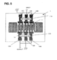
- Fig. 5 shows an example of the present invention applied to a longitudinal-mode coupling multimode surface acoustic wave filter provided with three (3) interdigital transducers and grating reflectors on both sides thereof;
- Fig. 6 is a diagram showing an example of an implementation of a surface acoustic wave apparatus to which the present invention is applied;
- Fig. 7 shows an embodiment which forms a varistor thin film on a surface of a package base;
- Fig. 8 shows an embodiment applying the present invention to an elastic wave apparatus using a film bulk acoustic resonator (FBAR); and
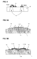
- Fig. 9A shows a first example of a configuration, which increases the varistor voltage without configuring the varistor thin film as a stacked layer.
- Fig. 9B shows a second example of a configuration, which increases the varistor voltage without configuring the varistor thin film as a stacked layer.
-
- Embodiments of the present invention will now be described with reference to the accompanying drawings.
- Fig. 1 is a block diagram showing a top view of a first embodiment of a surface acoustic wave apparatus according to the present invention. In Fig.1, a surface acoustic wave (SAW) element is formed on a
piezoelectric crystal substrate 1 such as quartz, LiTaO3 or LiNbO3. The surface acoustic wave (SAW) element has a resonator, which has opposinginterdigital electrodes reflectors resonator 2. - Electrodes constituting these
resonator 2 andreflectors piezoelectric crystal substrate 1 through the photolithography technology. - A varistor
thin film 17 is formed betweenvaristor terminal patterns bus bars interdigital electrodes varistor terminal patterns thin film 17 may be disposed upside down. - The varistor
thin film 17 refers to a thin-film object showing a nonlinear resistance property which drastically reduces a value of resistance when an applied voltage exceeds a varistor voltage Vv (and increases a current i), as shown in Fig.2. The materials include, for example, so-called semiconductor ceramics such as a zinc oxide with the addition of a minute amount of a lanthanum oxide, praseodymium oxide or cobalt oxide as an addition agent, and a strontium titanate. - A poly crystal ceramic thin film is made up of these materials by a sputtering method or sintering method. This ceramic is made up of crystal grains and grain boundaries, and Schottky barriers are formed in the grain boundary portion. High resistances are exhibited at the Schottky voltage or lower since electrons can not break through the barriers, however, lower resistances are exhibited at higher voltages since electrons breaks through the barriers and electric currents flow.
- Now, a method of fabrication for a thin-film varistor is considered. A proposition has been made for a method of a thin-film varistor at relatively low temperature with hydrothermal processing (see, e.g., Japanese Patent Application Laid-Open Publication No. 1993-299210). In the method, the hydrothermal processing is treated at temperatures higher than 100 °C.
- As this, generally, after varistor films are formed, the films must be burned at high temperatures or subjected to heat treatments at temperatures higher than 100 °C. However, after electrode patterns consisting mostly of Al are formed on the piezoelectric substrate, it is not desirable to raise the temperature of the substrate because of deterioration of the electrodes. Therefore, the varistor thin film can be formed at relatively lowtemperatures such as a room temperature or temperatures lower than 100 °C by use of the aerosol deposition method which forms fine thin films by reducing the burned or thermally treated varistor materials to micro powders and blowing the powders to the substrate placed in reduced-pressure atmosphere.
- In Fig. 1, when
bonding wires terminal pads interdigital electrode - According to the present invention, the
varistor terminal patterns interdigital electrodes thin film 17 is formed in the gap. Therefore, when high voltages are applied due to static electricity, the static charges flow through the varistorthin film 17 and destruction from discharges can be avoided at theinterdigital fingers - The varistor voltage can be changed by crystal grain diameters, grain boundaries and gap distances between the
varistor terminal patterns interdigital fingers thin film 17 can not be exerted since discharges between theinterdigital fingers thin film 17 exhibits low resistance even at the signal voltages applied to the surface acoustic wave element. - Therefore, the varistor voltage is desired to be 20 to 100 V for the surface acoustic wave filter in the frequency range of 1 to 2 GHz.
- Fig. 3 shows an embodiment applying the present invention to a ladder surface acoustic wave filter consisting of a plurality of one-port surface acoustic wave resonators. Fig. 4 is an equivalent circuit of the ladder surface acoustic wave filter of Fig. 3.
- A plurality of (e.g. four) one-port surface acoustic wave resonators SAW1 to SAW4 are connected by conductive patterns in parallel and serially to make up a band-pass filter on the
piezoelectric substrate 1.Terminal pads 181 to 184 on chips in outer edges are connected via bonding wires to package terminals, which are not shown. - Static electricity is transferred from outside via the package and bonding wire to an
input terminal pad 181 of the surface acoustic wave apparatus of Fig. 3, and a high voltage is applied between theinput terminal pad 181 and an input-sideground terminal pad 182 - If this high voltage exceeds the varistor voltage, a static charge flows through a varistor
thin film 171 to ground to protect the surface acoustic wave resonator SAW1 from the electrostatic discharges. - Also in this embodiment, in a second-level surface acoustic wave element SAW2, a varistor
thin film 172 is connected betweeninterdigital electrode fingers thin film 172 is not needed in principle. However, the varistorthin film 172 is useful for protection from destruction of the interdigital electrode fingers due to generated charges within elements, for example, high voltages due to pyroelectric effects generated by thepiezoelectric substrate 1. - Fig. 5 is an example of the present invention applied to a longitudinal-mode coupling multimode surface acoustic wave filter provided with three (3) interdigital transducers and grating reflectors on both sides thereof.
- When static electricity is applied to an
input terminal pad 185 configured on apiezoelectric crystal substrate 1, the static electricity is transferred to a center interdigital electrode, and difference in potential from an input-side ground pad 186 is applied between adjacentinterdigital electrode fingers - In Fig. 5, a pattern of a conductive film is not connected to the input-
side ground pad 186 on the surface of the surface acoustic wave chip. In this case, it is assumed that the input-side ground pad 186 is electrically connected with output-side ground pads thin film 174 on the input side between theinput terminal pad 185 and the output-side ground pads output terminal pads side ground pad 186, electrostatic destruction can be prevented in all the interdigital electrodes. - Fig. 6 is a diagram showing an example of an implementation of a surface acoustic wave apparatus to which the present invention is applied. This is an example in which flip chip implementation technology is applied to the surface acoustic wave apparatus structure according to the present invention in the implementation. This implementation technology is an implementation method which flips the surface acoustic
wave element chip 100 previously shown in Fig. 1 and Fig. 3 vertically and which connects theterminal pad 18 on the surface of thechip 100 with aconductive pattern 301 on apackage base 30 using abump 31 of a gold or solder ball without a bonding wire. Then, by covering with a cap or coating with resins, a small and thin surface acoustic wave filter is achieved. - The height of the
bump 31 of the gold and solder ball can maintain the gap between the surface of the surfaceacoustic wave chip 100 and the surface of thepackage base 30 on the order of 10 to 50 µm. Since the varistorthin film 17 formed on the surface acoustic wave chip surface is approximately 1 to 10 µm, the varistorthin film 17 does not contact with the surface of thepackage base 30. - In Fig. 6, the
conductive pattern 301 of the package base is connected to anexternal terminal 303 through a through-hole 302. - Fig. 7 is an embodiment, which forms the varistor
thin film 17 on the surface of thepackage base 30. In the embodiment shown in Fig. 1, after forming the conductive pattern of the surface acoustic wave electrode pattern on thepiezoelectric substrate 1 with the photolithography technology or the like, when the varistorthin film 17 is formed on the substrate surface, by exposing thepiezoelectric substrate 1 to high temperatures, the fine electrode pattern may be damaged, or the electrode may be destroyed by the pyroelectricity of the substrate. - Therefore, in this embodiment, the varistor
thin film 17 is formed on thepackage 30 side instead of the surface acoustic wave chip surface. In general, low-temperature co-fired ceramics (LTCC) or high-temperature co-fired ceramics (HTCC) are used as the material of thepackage base 30 of the surface acoustic wave element. Recently, other than above materials, silicon single crystals, glasses and sapphires are developed. Since each of these materials has excellent heat resistance, the degree of freedom is increased in setting up a temperature rising or temperature profile when the varistorthin film 17 is formed. - Therefore, varistor thin films can be formed which are excellent in terms of management of a crystal grain diameter and film quality and having less variation in the varistor characteristics.
- Also, if the
package base 30 is ceramics, a green sheet for the varistor thin film can be stacked with a green sheet for the firing of the package base to perform the firing at the same time. Other than forming on the surface of the package base, the varistor thin film may be embedded within the backside of the package base or the intermediate layer of the package base. - Subsequently, as shown in Fig. 6, connection is made to the surface acoustic wave chip 10 forming only the surface acoustic wave element via the
bump 31. - Although the above embodiments are mainly described with an example of the surface acoustic wave apparatus using the surface acoustic wave resonator, the application of the present invention is not limited to this and the present invention can be applied to an elastic wave apparatus using a film bulk acoustic resonator (FBAR).
- Fig. 8 is an embodiment applying the present invention to an elastic wave apparatus using a film bulk acoustic resonator (FBAR). The film bulk acoustic resonator (FBAR) is an element exhibiting a resonator property with elastic waves propagated within a thin film rather than surface waves.
- In Fig. 8, the
package base 30 hascavity regions 40 excavated by anisotropic etching at positions where the film bulk acoustic resonators (FBAR) are disposed. Also, the film bulk acoustic resonators FBAR1, FBAR2 are mounted on the upper side of the positions of thecavity regions 40 in thepackage base 30. When high voltages are applied to the film bulk acoustic resonators due to accumulated charges, the discharge breakdown may occur. Therefore, as is the case with the embodiments previously described, the varistorthin film 17 is formed on thepackage base 30 and connected between a hot electrode and a ground electrode of the necessary film bulk acoustic resonators FBAR1, FBAR2. - In this way, the discharge breakdown can be avoided in the film bulk acoustic resonators FBAR1, FBAR2.
- Now, it is necessary to increase a varistor voltage in order to adjust a discharge destroy voltage, if necessary. In this case, it is possible to increase the varistor voltage by stacking varistor thin films via conductive films as a multi layer to connect the varistor thin films in series. But, this may make the production costs high.
- Accordingly, Figs.9a, 9B indicate schematic diagrams of an embodiment which increases the varistor voltage without stacking the varistor thin film as a multilayer. Fig.9A shows an embodiment, in which the varistor voltage of the varistor
thin film 17 is increased in Fig. 1, and indicates a sectional view along the line A-B. - The Varistor
thin film 17 is connected to thevaristor terminal patterns electric pattern 117 is formed, at least a part of which is facing to thevaristor terminal patterns - At this time, an electric field applied on the varistor
thin film 17 due to static electricity comes to be connected in series between the portion "a" at which thevaristor terminal pattern 15 faces to theelectric pattern 117 and the portion "b" at which thevaristor terminal pattern 16 faces theelectric pattern 117. Thereby, the varistor voltage can be increased without stacking the varistor thin film and the conductive film as a multilayer. - Also, if the varistor voltage is more increased by increasing the number of serial stages, the
electric pattern 117 is divided intoelectrodes electric pattern 118 is formed having portions each facing theelectrodes - As described above, with the present invention, when static electricity with a voltage higher than the varistor voltage is applied, the resistance between the hot terminal and the ground terminal becomes low to pass the static charge to ground to enable the interdigital electrodes or the film bulk acoustic resonators of the surface acoustic wave element to be protected.
- Also, the thin film exhibiting varistor characteristics is integrally formed on the piezoelectric substrate onto which the surface acoustic wave element is formed and, therefore, destruction due to electrostatic discharges can be prevented at the time of a process for incorporating the relevant element into a mobile device or others. Therefore, it is expected that the reliability and production efficiency of cellular phones and others are improved.
- While illustrative and presently preferred embodiments of the present invention have been described in detail herein, it is to be understood that the inventive concepts may be otherwise variously embodied and employed and that the appended claims are intended to be construed to include such variations except insofar as limited by the prior art.
Claims (10)
- A surface acoustic wave apparatus comprising:a piezoelectric substrate;a surface acoustic wave element having at least one interdigital electrode made of a conductive film on the piezoelectric substrate; anda thin film electrically connected between terminals connecting to electrode fingers of the interdigital electrode, the thin film showing varistor characteristics and formed on the piezoelectric substrate.
- The surface acoustic wave apparatus according to claim 1, wherein the thin film showing the varistor characteristics is formed in a region of the piezoelectric substrate other than portions where the interdigital electrode is formed and portions where surface acoustic waves propagate.
- The surface acoustic wave apparatus according to claim 1 or 2, wherein the thin film showing the varistor characteristics is made up of semiconductor ceramics such as a zinc oxide or a strontium titanate to which a minute amount of an addition agent is added and which has a crystal grain diameter of 1 µm to 50 µm.
- The surface acoustic wave apparatus of claims 1, 2, or 3, wherein the thin film showing the varistor characteristics has a film thickness of 1 µm to 100 µm.
- The surface acoustic wave apparatus of claim 1, 2, 3, or 4, wherein the thin film showing the varistor characteristics is formed at room temperature by the aerosol deposition method which accelerates and causes micro powders of material showing varistor characteristics to collide against a substrate placed in reduced-pressure atmosphere.
- A surface acoustic wave apparatus comprising:a surface acoustic wave chip wherein a surface acoustic wave element having at least one interdigital electrode made up of a conductive film is formed on a piezoelectric substrate; anda package base substrate having a terminal electrode connected via a bump to a terminal electrode of the surface acoustic wave chip formed on the piezoelectric substrate, whereinon the package base substrate, a thin film showing the varistor characteristics is formed, which is electrically connected between electrode fingers of the interdigital electrode.
- The surface acoustic wave apparatus according to claim 6, wherein the thin film showing the varistor characteristics is formed on a top surface or an under surface of the package base substrate or within the substrate.
- An elastic wave apparatus comprising:a substrate having a cavity region excavated by anisotropic etching in the direction of thickness;a film bulk acoustic resonator disposed at a position corresponding to the cavity region of the substrate; anda thin film showing varistor characteristics formed on the substrate, the thin film electrically connected between terminals of the film bulk acoustic resonator.
- The surface acoustic wave apparatus of any of claims 1-7,
wherein the thin film showing varistor characteristics is electrically connected between the terminals connecting to electrode fingers of the interdigital electrode, and on the other side opposite to the one side, an electric pattern is formed, at least a part of which is facing to the terminals. - The elastic wave apparatus according to claim 8, wherein the thin film showing varistor characteristics is electrically connected between the terminals connecting to electrode fingers of the interdigital electrode, and on the other side opposite to the one side, an electric pattern is formed, at least a part of which is facing to the terminals.
Applications Claiming Priority (4)
| Application Number | Priority Date | Filing Date | Title |
|---|---|---|---|
| JP2004164100 | 2004-06-02 | ||
| JP2004164100 | 2004-06-02 | ||
| JP2005138836A JP4697528B2 (en) | 2004-06-02 | 2005-05-11 | Elastic wave device |
| JP2005138836 | 2005-05-11 |
Publications (1)
| Publication Number | Publication Date |
|---|---|
| EP1603233A1 true EP1603233A1 (en) | 2005-12-07 |
Family
ID=34941538
Family Applications (1)
| Application Number | Title | Priority Date | Filing Date |
|---|---|---|---|
| EP05253374A Withdrawn EP1603233A1 (en) | 2004-06-02 | 2005-06-01 | Saw apparatus and elastic wave apparatus |
Country Status (4)
| Country | Link |
|---|---|
| US (1) | US7190241B2 (en) |
| EP (1) | EP1603233A1 (en) |
| JP (1) | JP4697528B2 (en) |
| KR (1) | KR100643112B1 (en) |
Families Citing this family (7)
| Publication number | Priority date | Publication date | Assignee | Title |
|---|---|---|---|---|
| JP2004297619A (en) * | 2003-03-27 | 2004-10-21 | Kyocera Corp | Surface acoustic wave device |
| JP5039290B2 (en) * | 2005-08-25 | 2012-10-03 | 太陽誘電株式会社 | Filter and antenna duplexer |
| JP5141766B2 (en) * | 2008-07-10 | 2013-02-13 | 株式会社村田製作所 | Elastic wave device and ladder-type filter device |
| TWI566446B (en) * | 2013-11-20 | 2017-01-11 | 財團法人工業技術研究院 | Surface elastic wave generator, transceiver, and generation method thereof |
| JP6573853B2 (en) * | 2016-08-10 | 2019-09-11 | 太陽誘電株式会社 | Elastic wave device and manufacturing method thereof |
| JP7086592B2 (en) | 2016-12-21 | 2022-06-20 | スカイワークス ソリューションズ,インコーポレイテッド | Radio frequency system with overtemperature protection, surface acoustic wave filter and packaged module |
| KR20230103296A (en) | 2021-12-31 | 2023-07-07 | 삼성전기주식회사 | Acoustic resonator package |
Citations (5)
| Publication number | Priority date | Publication date | Assignee | Title |
|---|---|---|---|---|
| JPH0329407A (en) * | 1989-06-26 | 1991-02-07 | Mitsubishi Electric Corp | Surface acoustic wave generator |
| JPH08167826A (en) * | 1994-12-13 | 1996-06-25 | Nec Corp | Surface acoustic wave element |
| DE19631745C1 (en) * | 1996-08-06 | 1997-10-16 | Siemens Ag | Surface acoustic wave device with overload protection impedance |
| US20040021191A1 (en) * | 2002-07-30 | 2004-02-05 | Bradley Paul D. | Electrostatic discharge protection of thin-film resonators |
| US20040087286A1 (en) * | 2002-08-08 | 2004-05-06 | Tatsuya Inoue | High-frequency device |
Family Cites Families (11)
| Publication number | Priority date | Publication date | Assignee | Title |
|---|---|---|---|---|
| JPS55117293A (en) * | 1979-02-28 | 1980-09-09 | Matsushita Electric Ind Co Ltd | Piezoelectric vibrating unit |
| JPS5610725A (en) * | 1979-07-09 | 1981-02-03 | Murata Mfg Co Ltd | Elastic surface wave device |
| US4438417A (en) * | 1980-06-17 | 1984-03-20 | Tokyo Shibaura Denki Kabushiki Kaisha | Filter circuit utilizing a surface acoustic wave filter |
| JPS6178220A (en) * | 1984-09-26 | 1986-04-21 | Matsushita Electric Ind Co Ltd | surface wave filter |
| JPS6266605A (en) * | 1985-09-19 | 1987-03-26 | 富士電機株式会社 | Voltage nonlinear resistance element |
| JP2912081B2 (en) | 1992-04-16 | 1999-06-28 | 株式会社村田製作所 | Manufacturing method of thin film varistor and thin film varistor |
| DE4414160C1 (en) * | 1994-04-22 | 1995-12-21 | Siemens Matsushita Components | Component working with surface acoustic waves, in particular surface wave filters |
| JPH11274886A (en) * | 1998-03-26 | 1999-10-08 | Nec Shizuoka Ltd | Surface acoustic wave filter |
| JP2001127588A (en) * | 1999-10-28 | 2001-05-11 | Tdk Corp | Surface acoustic wave duplexer |
| JP2001168672A (en) | 1999-12-08 | 2001-06-22 | Matsushita Electric Ind Co Ltd | Surface acoustic wave device |
| JP3846406B2 (en) * | 2002-01-10 | 2006-11-15 | 株式会社村田製作所 | Electronic component, manufacturing method thereof, filter and duplexer using the same, and electronic communication device |
-
2005
- 2005-05-11 JP JP2005138836A patent/JP4697528B2/en not_active Expired - Fee Related
- 2005-05-27 US US11/138,422 patent/US7190241B2/en not_active Expired - Lifetime
- 2005-06-01 KR KR1020050046550A patent/KR100643112B1/en not_active Expired - Fee Related
- 2005-06-01 EP EP05253374A patent/EP1603233A1/en not_active Withdrawn
Patent Citations (5)
| Publication number | Priority date | Publication date | Assignee | Title |
|---|---|---|---|---|
| JPH0329407A (en) * | 1989-06-26 | 1991-02-07 | Mitsubishi Electric Corp | Surface acoustic wave generator |
| JPH08167826A (en) * | 1994-12-13 | 1996-06-25 | Nec Corp | Surface acoustic wave element |
| DE19631745C1 (en) * | 1996-08-06 | 1997-10-16 | Siemens Ag | Surface acoustic wave device with overload protection impedance |
| US20040021191A1 (en) * | 2002-07-30 | 2004-02-05 | Bradley Paul D. | Electrostatic discharge protection of thin-film resonators |
| US20040087286A1 (en) * | 2002-08-08 | 2004-05-06 | Tatsuya Inoue | High-frequency device |
Non-Patent Citations (2)
| Title |
|---|
| PATENT ABSTRACTS OF JAPAN vol. 015, no. 157 (E - 1058) 19 April 1991 (1991-04-19) * |
| PATENT ABSTRACTS OF JAPAN vol. 1996, no. 10 31 October 1996 (1996-10-31) * |
Also Published As
| Publication number | Publication date |
|---|---|
| JP4697528B2 (en) | 2011-06-08 |
| KR20060046351A (en) | 2006-05-17 |
| KR100643112B1 (en) | 2006-11-10 |
| JP2006020285A (en) | 2006-01-19 |
| US20050270124A1 (en) | 2005-12-08 |
| US7190241B2 (en) | 2007-03-13 |
Similar Documents
| Publication | Publication Date | Title |
|---|---|---|
| US7688161B2 (en) | Acoustic wave device and filter using the same | |
| EP2530838B1 (en) | Tunable filter | |
| EP1209807B1 (en) | Filter structure and arrangement comprising piezoelectric resonators | |
| US7477000B2 (en) | Surface acoustic wave device with electro-static discharge protection | |
| JP4518877B2 (en) | Surface acoustic wave device | |
| US7190241B2 (en) | Elastic wave apparatus | |
| JP2004297619A (en) | Surface acoustic wave device | |
| US7301421B2 (en) | Surface acoustic wave device, manufacturing method therefor, and communications equipment | |
| US20190123710A1 (en) | Surface acoustic wave devices using beryllium conductors | |
| CN100508386C (en) | elastic wave device | |
| JP4454410B2 (en) | Surface acoustic wave device, method of manufacturing the same, and communication device | |
| JP4458954B2 (en) | Surface acoustic wave device, method of manufacturing the same, and communication device | |
| JP4467403B2 (en) | Surface acoustic wave element and communication apparatus | |
| JP4610244B2 (en) | Manufacturing method of surface acoustic wave device | |
| KR100402066B1 (en) | A stack filter using FBAR | |
| US20250070749A1 (en) | Acoustic wave device and multiplexer | |
| JP4454411B2 (en) | Surface acoustic wave device, method of manufacturing the same, and communication device | |
| JP3290140B2 (en) | Method for manufacturing surface acoustic wave device | |
| KR102825977B1 (en) | Filters and Multiplexers | |
| KR102205988B1 (en) | SAW filter package and a method for manufacturing the same | |
| KR102066962B1 (en) | Filter including acoustic wave resonator | |
| JP2004235896A (en) | Surface acoustic wave device | |
| JP4514572B2 (en) | Surface acoustic wave device and communication device | |
| CN120185577A (en) | Elastic wave filter | |
| CN120074425A (en) | Acoustic filter device with low edge steepness |
Legal Events
| Date | Code | Title | Description |
|---|---|---|---|
| PUAI | Public reference made under article 153(3) epc to a published international application that has entered the european phase |
Free format text: ORIGINAL CODE: 0009012 |
|
| AK | Designated contracting states |
Kind code of ref document: A1 Designated state(s): AT BE BG CH CY CZ DE DK EE ES FI FR GB GR HU IE IS IT LI LT LU MC NL PL PT RO SE SI SK TR |
|
| AX | Request for extension of the european patent |
Extension state: AL BA HR LV MK YU |
|
| 17P | Request for examination filed |
Effective date: 20060606 |
|
| 17Q | First examination report despatched |
Effective date: 20060711 |
|
| AKX | Designation fees paid |
Designated state(s): DE FR GB |
|
| RAP1 | Party data changed (applicant data changed or rights of an application transferred) |
Owner name: TAIYO YUDEN CO., LTD. |
|
| GRAP | Despatch of communication of intention to grant a patent |
Free format text: ORIGINAL CODE: EPIDOSNIGR1 |
|
| RIC1 | Information provided on ipc code assigned before grant |
Ipc: H03H 9/02 20060101ALI20120330BHEP Ipc: H03H 9/64 20060101ALI20120330BHEP Ipc: H03H 9/05 20060101ALI20120330BHEP Ipc: H03H 9/58 20060101AFI20120330BHEP |
|
| STAA | Information on the status of an ep patent application or granted ep patent |
Free format text: STATUS: THE APPLICATION IS DEEMED TO BE WITHDRAWN |
|
| 18D | Application deemed to be withdrawn |
Effective date: 20120907 |