TECHNICAL FIELD
The present invention relates to a semiconductor laser
device, in particular, a multi-wavelength semiconductor laser
device made of a plurality of semiconductor laser elements that
oscillate at mutually different wavelengths, and a
manufacturing method thereof.
BACKGROUND ART
In an existing monolithic two-wavelength laser made of
two semiconductor laser elements, high reflectance coatings at
faces thereof are each formed as a film having a different
structure by making use of a mask. In the case of a
multi-layered film most suitable for a first wavelength being
formed, by covering a facet of the second semiconductor laser
element of the second wavelength with a mask, on the contrary,
in the case a multi-layered film most suitable for a second
wavelength being formed, by covering a facet of the first
semiconductor laser element of the first wavelength with a mask,
a high reflectance coating of the multi-layered film most
suitable for each is separately formed. A distance between
light emitting spots of two wavelengths of the monolithic
two-wavelength laser is one hundred and several tens
micrometers or less. Therefore, according to an existing method
in which films having different structures are separately
formed by use of the mask, high positioning accuracy is
necessary, resulting in poor productivity.
Furthermore, in order to enable to more improve the
productivity of two-wavelength semiconductor laser devices, a
resonator having a multi-layered reflective film that can be
used in two wavelength ranges has been proposed
(JP-A-2001-57413). This two-wavelength semiconductor laser
device has a structure of a multi-layered reflective film that
has a film thickness that an optical length to an average
wavelength λ of two wavelengths is (1/4 + j) × λ (j = 0, 1, 2,
...). The reason for adapting the film thickness to an average
wavelength of two wavelengths is that in a multi-layered film
of which wavelength is adapted to one wavelength range, the
reflectance to the other wavelength is extremely deteriorated.
However, in such two-wavelength semiconductor laser
device, since an average wavelength λ is deviated from both
wavelengths, it is difficult to obtain high reflectance close
to 100% for both wavelengths. In particular, in the case of
a two-wavelength semiconductor laser device having relatively
largely different wavelength ranges such as a 405 nm range and
a 650 nm range being manufactured, differences of the
respective wavelengths from the average wavelength become
large. Therefore, it is furthermore difficult to dispose high
reflectance multi-layered films to both wavelengths.
DISCLOSURE OF INVENTION
In order to solve the above-mentioned problems, the
present invention has an object, for example, to provide a
multi-wavelength semiconductor laser device that has high
reflectance multi-layered films that can be collectively
formed with the same structure on two or more semiconductor
laser element facets and a manufacturing method thereof.
According to the present invention, there is provided a
multi-wavelength semiconductor laser device comprising:
wherein the plurality of semiconductor laser elements
have a reflective film that is deposited on at least one of a
front facet and a backside facet thereof and has a multilayer
structure common to the semiconductor laser elements,
wherein the reflective film includes first and second
reflective regions disposed in a film thickness direction
thereof, the first reflective region having a first
predetermined reflectance to a first wavelength oscillated at
a first semiconductor laser element of the semiconductor laser
elements; and the second reflective region having a second
predetermined reflectance to a second wavelength that is
oscillated at a second semiconductor laser element other than
the first semiconductor laser element and different from the
first wavelength.
Furthermore according to the present invention, there is
provided a method of manufacturing a multi-wavelength
semiconductor laser device that includes a plurality of
semiconductor laser elements each of which oscillates at a
wavelength different from each other, comprising the steps of:
BRIEF DESCRIPTION OF THE DRAWINGS
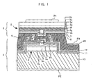
Fig. 1 is a schematic sectional view showing a
two-wavelength semiconductor laser device according to an
embodiment according to the present invention.
Fig. 2 is a schematic perspective view showing the
two-wavelength semiconductor laser device according to an
embodiment according to the invention.
Fig. 3 is a schematic sectional view showing a
multi-layered film of the two-wavelength semiconductor laser
device according to an embodiment according to the invention.
Fig. 4 is a flowchart showing a method of determining a
multi-layered film of the two-wavelength semiconductor laser
device according to an embodiment according to the invention.
Figs. 5 through 10 are flowcharts partially showing a
method of determining the multi-layered film of the
two-wavelength semiconductor laser device according to an
embodiment according to the invention.
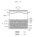
Fig. 11 is a schematic sectional view showing the
multi-layered film of the two-wavelength semiconductor laser
device according to an embodiment according to the invention.
Fig. 12 is a graph showing, of the reflectance of the
multi-layered film of the two-wavelength semiconductor laser
device according to an embodiment according to the invention,
dependency on film thickness of a phase adjustment region.
Fig. 13 is a schematic sectional view showing a
multi-layered film of a two-wavelength semiconductor laser
device according to another embodiment according to the
invention.
Fig. 14 is a graph showing, of the reflectance of the
multi-layered film of the two-wavelength semiconductor laser
device according to another embodiment according to the
invention, dependency on thickness in a phase adjustment
region.
Fig. 15 is a schematic perspective view showing a
two-wavelength semiconductor laser device according to still
another embodiment according to the invention.
DETAILED DESCRIPTION OF THE INVENTION
In the following, modes for carrying out the present
invention will be detailed with reference to attached drawings.
<Two-wavelength semiconductor laser device>
Fig. 1 is a sectional view showing an example in which
a multi-wavelength semiconductor laser device according to the
invention is applied to a two-wavelength semiconductor laser
device 1. Such a two-wavelength semiconductor laser device 1
has a hybrid structure in which a first light-emitting element
2 that is a GaN-based compound semiconductor laser (405 nm band
laser) and a second light-emitting element 3 that is an
AlGaInP-based compound semiconductor laser (650 nm band laser)
are solidly integrated with a fusing metal layer 4.
The first light-emitting element 2 includes a laser part
5 having a ridge stripe waveguide 6, and the second
light-emitting element 3 includes a laser part 9 that is formed
on an n-GaAs substrate 13 and has a ridge stripe waveguide 10.
Furthermore, an ohmic electrode P1 is formed on the laser
part 5, an ohmic electrode P2 is formed on the n-GaAs substrate
13, and an ohmic electrode P3 is formed on an exposed portion
4R of the fusing metal layer 4.
When a driving current is supplied through the ohmic
electrodes P1 and P3, 405 nm band laser light is emitted from
the first light-emitting element 2. And when a driving current
is supplied through the ohmic electrodes P2 and P3, 650 nm band
laser light is emitted from the second light-emitting element
3.
The laser part 5 of the first light-emitting element 2
has a multilayer structure in which a bottom layer 5b, an n-type
cladding layer 5c, an n-type guide layer 5d, an active layer
5e, an electron barrier layer 5f, a p-type guide layer 5g, a
p-type cladding layer 5h and a p-type contact layer 5i are
sequentially stacked in this order, wherein the p-type contact
layer 5i and the p-type cladding layer 5h are partially etched
and removed, and thereby the above ridge waveguide 6 is formed
in a stripe shape that extends from this side of paper space
toward a back side thereof.
Except for the p-type contact layer 5i of the ridge
waveguide 6, on the whole surface of the p-type cladding layer
5h, an insulating layer 7 is formed, and further, on the whole
surface of the p-type contact layer 5i and the insulating layer
7, an ohmic electrode layer 8 is formed.
Accordingly, the ridge waveguide 6 is electrically
connected through the p-type contact layer 5i and the ohmic
electrode layer 8 to the fusing metal layer 4.
More specifically, the bottom layer 5b is made of
Si-doped n-type GaN and formed into a thickness in the range
of substantially 5 to 15 µm. The n-type cladding layer 5c is
made of n-type Al0.08Ga0.92N and formed into a thickness of
substantially 0.8 µm. The n-type guide layer 5d is made of
n-type GaN and formed into a thickness of substantially 0.2 µm.
The active layer 5e has a thickness of substantially
several tens nanometers and a multiple quantum well structure
that includes a well layer and a barrier layer that are made
of InxGa1-xN (0 ≤ x) different in the composition from one
another, such as In0.08Ga0.92N and In0.01Ga0.99N. The electron
barrier layer 5f is made of AlGaN and has a thickness of
substantially 0.02 µm. The p-type guide layer 5g is made of
Mg-doped p-type GaN and has a thickness of substantially 0.02
µm.
The p-type cladding layer 5h is made of p-type Al0.08Ga0.92N
and has a thickness of substantially 0.4 µm. The p-type contact
layer 5i is made of p-type GaN and has a thickness of
substantially 0.1 µm.
Furthermore, the ohmic electrode layer 8 is made of any
one of Pd, Pt, Au or Ni or an alloy thereof, and the insulating
layer 7 is made of SiO2 or the like.
Still furthermore, the fusing metal layer 4 is made of
an alloy that is generated by fusing a fusing metal layer 4a
made of Au and a fusing metal layer 4b made of Sn.
The laser part 9 of the second light-emitting element 3
has a multilayer structure in which on an n-type GaAs substrate
13, a n-type buffer layer 9a, an n-type cladding layer 9b, an
active layer 9c, a p-type cladding layer 9d, a smoothing layer
9e and a p-type contact layer 9f are deposited in this order.
Subsequently, by removing the p-type contact layer 9f and
the smoothing layer 9e and a part of the p-type cladding layer
9d by means of the etching or the like, the ridge waveguide 10
is formed in a stripe shape that extends from this side of the
paper space to a back side thereof. Furthermore, after the
ridge waveguide 10 is formed, with a region where the laser part
9 is to be formed and the ridge waveguide 10 masked, a non-masked
region is etched to a relatively deep portion of the n-type GaAs
substrate 13, and thereby the laser part 9 having a projected
sectional shape as shown in Fig. 1 is formed.
An entire surface of the laser part 9 and the n-type GaAs
substrate 13 except for the p-type contact layer 9f is covered
with an insulating layer 11, and furthermore an ohmic electrode
layer 12 is deposited on an entire surface of the p-type contact
layer 9f and the insulating layer 11, and thereby the p-type
contact layer 9f is electrically connected to the ohmic
electrode layer 12 and further connected electrically through
the ohmic electrode layer 12 to the fusing metal layer 4.
More specifically, the buffer layer 9a is made of
Si-doped n-type GaAs and formed into a thickness of
substantially 0.5 µm. The n-type cladding layer 9b is made of
n-type Al0.35Ga0.15 In0.5P and formed into a thickness of
substantially 1.2 µm.
The active layer 9c has a thickness of substantially ten
and several nanometers and a strained quantum well structure
made of GaInP and AlGaInP . The p-type cladding layer 9d is made
of Zn-doped p-type Al0.35Ga0.15 In0.5P and has a thickness of
substantially 1.2 µm. The smoothing layer 9e is made of p-type
Ga0.51In0.49P and has a thickness of substantially 0.05 µm. The
p-type contact layer 9f is made of p-type GaAs and has a
thickness of substantially 0.2 µm.
Furthermore, the ohmic electrode layer 12 is made of any
one of Ti, Pt, Cr, Au or Au-Zn or an alloy thereof, and the
insulating layer 7 is made of SiO2 or the like.
In manufacturing the two-wavelength semiconductor laser
provided with the first and second light-emitting elements 2,
3, shown in Fig. 1, for instance, there are used a bonding
technique with a fusing metal (fusing metal layer 4) and a laser
liftoff technique as a removal technique of a substrate on which
a GaN-based compound semiconductor is epitaxialy grown.
The first light-emitting element 2 is manufactured in
such a way that, on a sapphire substrate, layers from the bottom
layer 5b to the p-type contact layer 5i are deposited by means
of MOCVD process or the like, followed by etching to form the
laser part 5 and the ridge waveguide 6, and on the entire surface
thereof, the insulating layer 7, the ohmic electrode layer 8
and the fusing metal layer 4 are sequentially deposited.
The second light-emitting element 3 is manufactured in
such a way that, on the n-type GaAs substrate 13, layers from
the n-type buffer layer 9a to the p-type contact layer 9f are
deposited by means of MOCVD process or the like, followed by
etching to form the laser part 9 and the ridge waveguide 10,
and over the entire surface thereof, the insulating layer 11,
the ohmic electrode layer 12 and the fusing metal layer 4 are
sequentially deposited.
Wafers of the first and second light-emitting elements
2 and 3 are bonded through the respective fusing metal layers
4.
The sapphire substrate of the first light-emitting
element 2 is removed by use of laser lift-off process. That
is, UV light that transmits sapphire and is absorbed by GaN is
irradiated from the back surface of the sapphire substrate to
decompose GaN in the vicinity of the interface of sapphire and
GaN, and thereby the sapphire substrate is peeled. At this time,
in a region other than the laser part 9, the first
light-emitting element 2 is not fused. Therefore, in the region,
the exposure portion 4R of the fusing metal layer is formed.
By cleaving the GaAs substrate 13, a resonator facet is
formed. The cleaved substrate i.e., a laser bar carrying
semiconductor laser elements that oscillate at different
wavelengths is formed.
As shown in Fig. 2, on every facet of the resonator, a
reflective film is collectively formed for each facet by means
of sputtering process and so on. Here, a facet of laser diode
is coated with a low reflectance film made of a single layer
film of alumina, for example, and a backside facet is formed
as a high reflectance film made of a multi-layered film
described later. Since the resonator facet is formed by
cleaving the GaAs substrate 13, the light emitting spots of the
two light-emitting elements are in the same plane. The first
light-emitting element 2 oscillates laser light having a
wavelength λ1 = 405 nm, and the second light-emitting element
3 oscillates laser light having a wavelength λ2 = 650 nm.
<Multi-layered film of backside facet>
A structure of the multi-layered film (reflective film)
of the backside facet in the two-wavelength semiconductor laser
device is in common for the two semiconductor laser elements
and, as shown in Fig. 3, constituted of, for instance, three
regions. That is, the multi-layered film 12 includes a first
reflective region 121 that is constituted of dielectric films
1Di1, ... 1Dik deposited in k layers on a side that is in contact
with a semiconductor Semi that is a semiconductor laser body;
and a second reflective region 122 that is constituted of
dielectric films 2Di1, ... 2Di1 deposited in 1 layers that are
more separated from the semiconductor Semi than the first
reflective region.
Each of the dielectric films 1Di1, ... 1Dik of the first
reflective region 121 has a predetermined optical thickness
(refractive index × film thickness) to the first wavelength λ1,
and the predetermined optical thicknesses are each set at (2p
+ 1)/4 × λ1 (wherein p = 0, 1, 2, ...). Each of the dielectric
films 2Dil, ... 2Dil of the second reflective region 122 has a
predetermined optical thickness to the second wavelength λ2,
and the predetermined optical thicknesses are each set at (2q
+ 1) / 4 × λ2 (wherein q = 0, 1, 2, ...). In order to obtain
refractive index steps, each of the dielectric films is set
differently in the refractive index from adjacently ones.
Therefore, the respective film thicknesses become different
from one another.
In the above structure, the phases of lights reflected
by the first reflective region 121 and the second reflective
region 122 are not always coincident with each other.
Accordingly, the multi-layered film 12 may further contain a
phase adjustment region 123 between the reflective regions 121
and 122. Since light radiated from the semiconductor has two
wavelengths λ1, λ2, within a range that makes the respective
phase differences of both wavelengths smaller, an optical
thickness of the phase adjustment region 123 is determined. The
phase adjustment region 123 is made of a single layer dielectric
film that is either higher or lower in the refractive index than
both dielectric films in the first and second reflective
regions 121, 122 that come into contact therewith.
Another method of determining the optical thickness of
the multi-layered film 12 is carried out as follows. That is,
in a system where the first reflective region is present on the
semiconductor and there exists infinite phase adjustment
region thereon, the first reflective region is constituted of
a multi-layered film the reflectance of which, seen from the
semiconductor, becomes substantially the same as the first
predetermined reflectance R1 to the first wavelength λ1.
The second reflective region is constituted of such a
multi-layered film, in a system where the second reflective
region is present on the phase adjustment region, the
reflectance of which, seen from the phase adjustment region,
becomes substantially the same as the second predetermined
reflectance R2 to the second wavelength λ2.
As to the optical thickness of the phase adjustment
region, the film thickness d3 and the refractive index n3
defining the optical thickness are determined such that the
reflectance of a reflective film as a whole becomes the first
predetermined reflectance R1 to the first wavelength λ1 and the
second predetermined reflectance R2 to the second wavelength
λ2.
<Example of determination of multi-layered film>
The method of determining a multi-layered film according
to the invention will be explained based on a flowchart shown
in Fig. 4.
As a first step (S1), in order that for all of the first
and second reflective regions as well as the phase adjustment
region, a high refractive index material and a low refractive
index material are alternately disposed, dielectrics materials
of the respective layers are determined. In k layers of
dielectrics in the first reflective region, their refractive
indices are denoted as n11, n12, ... n1k to the first wavelength
and m11, m12, ... m1k to the second wavelength, and their
thicknesses are in terms of d11, d12, ... d1k . In 1 layers of
dielectrics in the second reflective region, their refractive
indices are denoted as n21, n22, ... n21 to the first wavelength
and m21, m22, ... m21 to the second wavelength, and their
thicknesses are in terms of d21, d22, ... d21 · In the phase
adjustment region, its refractive index is denoted as n3 to the
first wavelength and m3 to the second wavelength, and its
thickness is in terms of d3.
In the next place, as a second step (S2), film thicknesses
d21, d22, ... d21 of the respective layers in the second reflective
region 122 are determined so that the optical thicknesses
become (2p + 1) /4 × λ2 (wherein p = 0, 1, 2, ...) to the second
wavelength λ2.
Next, as a third step (S3), the reflectances R12, R22 of
the second reflective region to the first and second
wavelengths λ1, λ2 seen from the single layer phase adjustment
region (refractive indices to the first and second wavelengths:
n3 and m3) are calculated, respectively. In the third step,
as shown in Fig. 5, the refractive index n3 of the phase
adjustment region to the first wavelength and the reflectance
of an initial layer are initially set (S31), then the amplitude
reflectance R2j is repeatedly calculated based on the
reflectance r2j + 1 and the phase retardation δj of the respective
layers up to the predetermined 1 layer (S32). On reaching the
1 layer (S33), the reflectance R12 of the second reflective
region to the first wavelength can be obtained (S34) . Further,
similarly, as shown in Fig. 6, the refractive index m3 of the
phase adjustment region to the second wavelength and the
reflectance of an initial layer are initially set (S311), then
the amplitude reflectance R2j is repeatedly calculated based
on the reflectance r2j+1 and the phase retardation δj of the
respective layers up to the predetermined 1 layer (S321). On
reaching the 1 layer (S331), the reflectance R22 of the second
reflective region to the second wavelength can be obtained
(S341).
Subsequently, as a fourth step (S4) shown in Fig. 4, with
the film thickness of the single layer phase adjustment region
as variable x, the reflectances R13 (x), R23 (x) to the first
and second wavelengths λ1, λ2 of the phase adjustment region
and the second reflective region seen from the first contact
region in the first reflective region with the phase adjustment
region (refractive indices to the first and second wavelengths:
n11 and m11) are calculated by use of the reflectances R12, R22.
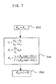
In the fourth step, as shown in Fig. 7, the reflectance R12 is
set as an initial value (S41), then the amplitude reflectance
R3 is calculated based on the single layer reflectance r3 and
the phase retardation δ3 (S42), and thereby a result to the first
wavelength, R3 = R13 (x), can be obtained (S43) . Furthermore,
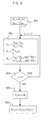
similarly to the above, as shown in Fig. 8, the reflectance R22
is set as an initial value (S411), then the amplitude
reflectance R3 is calculated based on the single layer
reflectance r3 and the phase retardation δ3 (S421), and thereby
a result to the second wavelength, R3 = R23 (x), can be obtained
(S431).
In the next place, as a fifth step (S5) shown in Fig. 4,
the film thicknesses d11, d12, ... d1k of the respective layers in
the first reflective region 121 are determined so that the
optical thickness becomes (2q + 1) /4 × λ1 (wherein, q = 0, 1,
2, ...) to the first wavelength λ1 (S5).
Subsequently, as a sixth step (S6), the reflectances R1
(x), R2 (x) of the multi-layered film as a whole for each
wavelength seen from the semiconductor to the first and second
wavelengths λ1, λ2, (reflectances to the first and second
wavelengths: nsem1 and msem1) respectively, are calculated with
the obtained reflectances R13 (x), R23 (x), and thereby the
energy reflectances F1 (x) = R1 (x) × R1 (x) *, F2 (x) R2 (x)
× R2 (x) * are obtained. Here, the R1 (x) * and R2 (x) * denote
complex conjugate values of the R1 (x), R2 (x), respectively.
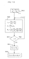
In the sixth step, as shown in Fig. 9, to the first wavelength,
the reflectance nsem1 of the semiconductor to the first
wavelength and the obtained reflectance R13 (x) are set as
initial values (S61), then the amplitude reflectance R1j is
repeatedly calculated based on the reflectance r1j + 1 and the
phase retardation δj of the respective layers up to the
predetermined k layer (S62). Upon reaching the k layer (S63),
the reflectance R1 (x) of the whole multi-layered film to the
first wavelength is obtained (S64). Subsequently, the energy
reflectance F1 (x) = R1 (x) × R1 (x) * to the first wavelength
is calculated (S65). Furthermore, similarly to the above, as
shown in Fig. 10, to the second wavelength, the reflectance msemi
of the semiconductor to the second wavelength and the obtained
reflectance R23 (x) are set as initial values (S611), then the
amplitude reflectance R1j is repeatedly calculated based on the
reflectance r1j+1 and the phase retardation δj of the respective
layers up to the predetermined k layer (S621). Upon reaching
the k layer (S631), the reflectance R2 (x) of the whole
multi-layered film to the second wavelength is obtained (S641).
Subsequently, the energy reflectance F2(x) = R2(x) × R2 (x) *
to the second wavelength is calculated (S651).
In the next place, as a seventh step (S7) shown in Fig.
4, since the reflectance of the multi-layered film as a whole
to each of the first and second wavelengths λ1, λ2 varies
according to the film thickness x of the single layer phase
adjustment region, a range of the film thickness x of the phase
adjustment region where high reflectance can be obtained to
each of the wavelengths is calculated. That is, with x that
satisfies F1' (x) = 0 and F1' ' (x) < 0 as d1p, a range of x, d1min
≤ x ≤ d1max, that satisfies F1 (x) ≥ F1(d1p) × a, is obtained.
Furthermore, with x that satisfies F2' (x) = 0 and F2" (x) <
0 as d2p, a range of x, d2min ≤ x ≤ d2max, that satisfies F2 (x)
≥ F2(d2p) × a is obtained (S7). Here, a can be set at, for
instance, 0.95.
Subsequently, as an eighth step (S8) shown in Fig. 4, the
film thickness of the phase adjustment layer is determined in
the range that satisfies d1min ≤ x ≤ d1max and d2min ≤ x ≤ d2max.
According to the present invention, even when two or more
wavelengths are relatively largely different from each other,
a multi-layered film structure that can be high in the
reflectance to a plurality of wavelengths can be attained.
<Embodiments>
With the first and second wavelengths λ1 and λ2 set at
405 nm and 650 nm respectively, a two-wavelength semiconductor
laser device is designed and manufactured.
In Fig. 11, a configuration example (I) of a
multi-layered film of a two-wavelength semiconductor laser
device according to an embodiment is shown. A first reflective
region 121 in contact with a semiconductor Semi has a structure
of four layers and is made of dielectric films 1Di1, ... 1Di4.
A second reflective region 122 deposited more separated from
the semiconductor Semi than the first reflective region is made
of three layers of dielectric films 2Di1, ... 2Di3. A phase
adjustment region 123 between the both reflective regions is
a single layer.
The first reflective region 121 that is in contact with
the semiconductor is designed so as to be high in the
reflectance to the wavelength 405 nm. Specifically, a
dielectrics that is low in the refractive index to the
wavelength 405 nm and a dielectrics that is high in the
refractive index thereto are alternately deposited with film
thicknesses such that the respective optical thicknesses
(refractive index × film thickness) become (2p + 1) /4 × 405 nm
(wherein, p = 0, 1, 2, ...). For instance, when SiO2 and TiO2,
respectively, are used as a low refractive index dielectrics
material and a high refractive index material, the refractive
indices to wavelength 405 nm, respectively, are 1.47 and 2.98.
Accordingly, film thicknesses where the optical thicknesses
become 101 nm at p = 0 in the above equation become 69 nm and
34 nm, respectively. Accordingly, as shown in Fig. 11, with
these film thicknesses of 69 nm and 34 nm, each of dielectric
films of SiO2 and TiO2 is alternately deposited as to be 1Di1,
... 1Di4. The second reflective region 122 that is in contact
with air is designed so as to be high in the reflectance to the
wavelength 650 nm. Specifically, a dielectrics that is low in
the refractive index to the wavelength 650 nm and a dielectrics
that is high in the refractive index thereto are alternately
deposited with film thicknesses such that the respective
optical thicknesses (refractive index × film thickness) become
(2q + 1)/4 × 650 nm (wherein, q = 0, 1, 2, ...). For instance,
when SiO2 and TiO2 are used as a low refractive index dielectrics
material and a high refractive index material respectively, the
refractive indices to the wavelength 650 nm, respectively, are
1.45 and 2.57. Accordingly, film thicknesses where the optical
thicknesses become 162 nm at q = 0 in the above equation become
112 nm and 63 nm, respectively. Accordingly, as shown in Fig.
11, with these film thicknesses of 112 nm and 63 nm, each of
dielectric films of SiO2 and TiO2 is alternately deposited to
be 2Di1, ... 2Di3. That is, in the multi-layered structure shown
in Fig. 11, the dielectric film of the first reflective region
121 is formed into a multi-layered film made of two pairs of
SiO2 (69 nm) and TiO2 (34 nm), the second reflective region 122
is formed into a multi-layered film made of TiO2 (63 nm)/SiO2
(112 nm)/TiO2 (63 nm), and a film thickness of the phase
adjustment layer 123 that is, for instance, a single layer film
of SiO2 is set at x (nm).
The film thickness x of a single layer of the phase
adjustment region 123 that uses SiO2 as the dielectrics is
determined based on the flowchart shown in Fig. 4. In this case,
the reflectance of the multi-layered film 12 of the
two-wavelength semiconductor laser device exhibits the
dependency on the film thickness x of the phase adjustment
region. That is, as shown in Fig. 12, since the reflectance
periodically varies with the film thickness x of the phase
adjustment region 123 for each of oscillation wavelengths, the
film thickness x of the phase adjustment region is determined
in the vicinity of the peak thereof. For instance, as obvious
from Fig. 12, in the film thickness of 50 nm, the reflectance
of 94% is obtained to the wavelength 405 nm and that of 80% is
obtained to the wavelength of 650 nm. This film thickness is
selected for the phase adjustment region. In practice,
according to the first and second wavelengths, 405 nm and 650
nm, periods of the reflectance variation are different from
each other. Therefore, the film thickness of the phase
adjustment region is selected so that the reflectance may be
high for both the wavelengths. A range of the film thickness
x of the phase adjustment region 123 where, for instance, 95%
or more of the peak intensity can be obtained is 17 nm ≤ x ≤
91 nm for the wavelength of 405 nm and 0 nm ≤ x ≤ 98 nm for the
wavelength of 650 nm. Accordingly, the film thickness is
selected among these. Thus, as to the film thickness x of the
phase adjustment region 123, a range of the film thickness where
the predetermined ratio of the peak intensity can be obtained
in each of the wavelengths is obtained, and from a region where
the film thickness ranges overlap each other, the film
thickness x can be selected.
In Fig. 13, a configuration example of a multi-layered
film (II) of a two-wavelength semiconductor laser device
according to another embodiment is shown. Dielectrics films
1Di1, ... 1Di6 of the first reflective region are formed into a
multi-layered film of three pairs of SiO2 (69 nm) and TiO2 (34
nm), that is, 6 layers. The dielectric films 2Di1, ... 2Di5 of
the second reflective region are formed into a multi-layered
film of TiO2 (63 nm)/SiO2 (112 nm) /TiO2 (63 nm)/SiO2 (112
nm) /TiO2 (63 nm), that is, 5 layers. And the phase adjustment
region is made of a single layer film of SiO2 having a film
thickness x (nm). As shown in Fig. 14, the reflectance of the
multi-layered film 12 exhibits the dependency on the film
thickness x of the phase adjustment region. Accordingly, a
range of the film thickness x where the intensity becomes, for
instance, 95% or more of the peak intensity is 25 nm ≤ x ≤ 140
nm for the wavelength of 405 nm and 75 nm ≤ x ≤ 190 nm for the
wavelength of 650 nm. Accordingly, the film thickness is
selected of the overlap thereof. For instance, at the film
thickness of 100 nm, values of the reflectance to wavelengths
405 and 650 nm are 98% and 96%, respectively. Therefore, very
high reflectance can be obtained for both wavelengths.
As another embodiment, in a two-wavelength semiconductor
laser device according to a configuration example of
multi-layered film (III), similarly to the above embodiment,
the multi-layered film has a structure that includes a first
reflective region in contact with the semiconductor and made
of dielectric films of 2.5 pairs of SiO2 (69 nm)/TiO2 (34 nm),
that is, 5 layers. A second reflective region deposited more
separated from the semiconductor than the first reflective
region and made of dielectric films of two pairs of SiO2 (112
nm)/TiO2 (63 nm), that is, 4 layers. And a phase adjustment
region TiO2 (75 nm) between both reflective regions.
The values of reflectance to the
wavelengths 405 nm and
650 nm in the configuration examples (I), (II) and (III) of the
above multi-layered films are summarized in Tables 1, 2 and 3.
| Configuration example I | Light reflectance at 405 nm | Light reflectance at 650 nm |
| | Dielectrics | Film thickness (nm) | Repetition number of layers | 94% | 80% |
| First reflective region | SiO2 | 69 | 2 pairs |
| TiO |
| 2 | 34 |
| Phase adjustment region | SiO | 2 | 50 |
| Second reflective region | TiO2 | 63 | 1.5 pairs |
| SiO2 | 112 |
| Configuration example II | Light reflectance at 405 nm | Light reflectance at 650 nm |
| | Dielectrics | Film thickness (nm) | Repetition number of layers | 98% | 96% |
| First reflective region | SiO2 | 69 | 3 pairs |
| TiO |
| 2 | 34 |
| Phase adjustment region | SiO | 2 | 100 |
| Second reflective region | TiO2 | 63 | 2.5 pairs |
| SiO2 | 112 |
| Configuration example III | Light reflectance at 405 nm | Light reflectance at 650 nm |
| | Dielectrics | Film thickness (nm) | Repetition number of layers | 95% | 92% |
| First reflective region | SiO2 | 69 | 2.5 pairs |
| TiO |
| 2 | 34 |
| Phase adjustment region | TiO | 2 | 75 |
| Second reflective region | SiO2 | 112 | 2 pairs |
| TiO2 | 63 |
In the above embodiments, cases where SiO2 and TiO2 are
used as the materials of the multi-layered films are explained.
However, materials such as Al2O3, ZrO2 , Si3N4, Ta2O5 and so on
may be used in appropriate combinations.
A reflective region of a quarter-wave film to a short
wavelength and a reflective region of a quarter-wave film to
a long wavelength may be deposited in either order. However,
in the first reflective region, when the low reflectance is set
to the second wavelength (wavelength 650 nm in the above
embodiment), over a wide range of the film thickness x of the
phase adjustment region, the reflectance of the multi-layered
film 12 to the second wavelength can be made higher. The
dielectrics multi-layered film is easy in designing the
reflectance high to short wavelengths with low to long
wavelengths. Accordingly, as to the order of deposition of the
first reflective region and the second reflective region, it
is preferable to form a quarter-wave film to the short
wavelength in the first reflective region and a quarter-wave
film to the long wavelength in the second reflective region.
A case where as to an order of deposition of the first reflective
region and the second reflective region, a quarter-wave film
to the short wavelength is formed in the first reflective region
and a quarter-wave film to the long wavelength is formed in the
second reflective region was explained. In another embodiment,
even if the second wavelength is reflected by the first
reflective region, as far as the phase difference of reflected
light from the first reflective region and reflected light from
the second reflective region can be sufficiently adjusted in
the phase adjustment region, high reflectance can be obtained
even to the second wavelength. Accordingly, the reflective
region of a quarter-wave film to a short wavelength and the
reflective region of a quarter-wave film to a long wavelength
may be deposited in whatever order.
Furthermore, in the above embodiments, the phase
adjustment region is disposed between the first reflective
region and the second reflective region. However, depending
on the number of layers in the first and second reflective
regions, in some cases, when the film thickness of the phase
adjustment region is zero, the phase difference of both
wavelengths becomes smaller. In this case, the multi-layered
film is formed with the first and second reflective regions in
direct contact.
Still furthermore, the two-wavelength semiconductor
laser device has been explained above, however, the present
invention can be applied also to multi-wavelength
semiconductor laser devices having three or more semiconductor
laser elements.
According to a multi-wavelength laser of the invention,
multi-layered films at facets of a resonator may be obtained
with high reflectance to all of a plurality of wavelengths.
Therefore, the characteristics of all laser elements can be
improved. Furthermore, since the film formation can be
collectively performed to all of the laser elements, the
productivity can be also improved.
Furthermore, even in the case where a distance between
light emitting spots is so small (for instance 50 µm or less)
that a conventional method in which films of different
structures are separately formed by use of masks can be hardly
applied, according to the invention, a multi-layered film that
has high reflectance to both wavelengths can be easily
manufactured. Still furthermore, even in the case where
difference of two wavelength ranges is so large (for instance,
405 nm band and 650 nm band) that a conventional method in which
a film is designed so as to adapt to an average wavelength of
two wavelengths can be applied with difficulty, the
multi-layered film according to the invention can obtain
sufficient characteristics.
The two-wavelength semiconductor laser device shown in
Fig. 1 is manufactured by bonding two semiconductor laser
elements formed on separate substrates. However, in another
embodiment, as shown in Fig. 15, the two-wavelength
semiconductor laser device may have a monolithic structure in
which two ridge type semiconductor laser elements that
oscillate at wavelengths λ1 and λ2, which are different from
each other such as 650 nm and 780 nm, are formed on the same
substrate with an isolation groove intervened therebetween. As
materials that constitute each of active layers of a plurality
of semiconductor laser elements, other than GaN and AlGaInP,
any material that can be used in the relevant field, such as
AlGaAs materials, InGaAsP materials, PbSnTe materials, can be
used. By appropriately adjusting compositional ratios of these
materials, semiconductor laser elements having an active layer,
a cladding layer and so on that have desired characteristics
can be obtained. Furthermore, an active layer of a
semiconductor laser diode may have, other than a multiple
quantum well structure, a structure such as a single quantum
well structure, a bulk active layer structure and so on.