TECHNICAL FIELD
The present invention relates to a connection structure between a coaxial connector
and a multilayer board for use in, for example, a high-frequency circuit of a
communication device and so on.
BACKGROUND ART
In a conventional connection structure between a coaxial connector and a multilayer
board, the signal line pattern of the transmission line (hereinafter, referred to as
'electroconductive pattern') of a high-frequency multilayer board (hereinafter, referred
to as 'multilayer board') mounted in an electroconductive casing and the core wire of a
coaxial connector have been directly electrically connected by use of suitable brazing
material (see, for instance, JP-A-2001-177311).
The operation will now be described as below.
A high frequency signal input from the coaxial connector passes the connection
between the coaxial connector and the multilayer board, and propagates through the
transmission line formed on the multilayer board; and also in the propagating line in
the direction opposite thereto, a high frequency signal that has propagated through the
transmission line passes the connection between the coaxial connector and the
multilayer board, and propagates toward the coaxial connector.
In the above operation, in the connecting portion between the coaxial connector and
the multilayer board, the spacing between the grounding face on the casing and the
core wire of the coaxial connector becomes large because the multilayer board has its
thickness, to thereby cause the impedance of the transmission line in this area to be
greatly disordered, and induce the transmission line to be dielectric. Here, there is a
trend toward larger degree of the dielectric property thereof with increasing thickness
of the multilayer board. In addition, in the multilayer board, because it is difficult to
form the transmission line pattern in the uppermost layer of this board and the ground
pattern in the layer located immediately under the layer closely to the end face of the
board, a large pattern margin forms between the end face of the board and the end of
the ground pattern. For this reason, in the vicinity of the end face of the multilayer
board, it is impossible to form the ground pattern constituting the transmission line.
Therefore, there arises a problem that the impedance of the transmission line is greatly
disordered also in this area to thereby induce the transmission line to be dielectric.
On this account, in the conventional connection structure between the coaxial
connector and the multilayer board, it is arranged that the coaxial connector is
equipped with a capacitive coaxial line in order to cancel the above-mentioned
dielectric property of the transmission line, and thereby an impedance match is
schemed to ensure its performance capabilities.
The conventional connection structure between the coaxial connector and the
multilayer board has been arranged as mentioned above. As a result, around the
frequencies designed such that the impedance match is provided, the capacitive coaxial
line provided on the coaxial connector and the dielectric transmission line provided in
the connection between the coaxial connector and the multilayer board mutually cancel
the capacitive property and the dielectric property to thus render the matching. This
reduces the disorder of impedance, thereby enabling the obtainment of a certain level
of return-loss characteristic. However, at frequencies away from the designed
frequencies, the match cannot be provided, and the disorder of impedance in the
connection between the coaxial connector and the multilayer board increases, thereby
making it impossible to obtain the low return-loss characteristic indispensable to the
high-frequency circuit. From these factors, in the conventional connection structure
between the coaxial connector and the multilayer board, it is very difficult to obtain
favorable return-loss characteristics over a wide frequency band. As a result, there is a
problem that countermeasures to development of broadband in communication
equipments seen in recent years cannot be implemented.
The present invention has been accomplished to solve the above-mentioned problem.
An object of the present invention is to provide a connection structure between a
coaxial connector and a multilayer board that can greatly reduce the disorder of
impedance due to the electrical connecting portion between the coaxial connector and
the board, and that can obtain an excellent return-loss characteristic over a broad band.
DISCLOSURE OF THE INVENTION
According to one aspect of the present invention, there is provided a connection
structure between a coaxial connector and a multilayer board, the connection structure
including: a casing; a coaxial connector that is provided in this casing, and has a core
wire; a multilayer board that is provided in the casing, and has a first signal line
pattern; a transfer board that is provided in the casing located between this multilayer
board and the coaxial connector, has a second signal line pattern, and that is formed so
that the thickness of the transfer board is smaller than the thickness of the multilayer
board; a connecting means for electrically connecting the core wire of the coaxial
connector and the second signal line pattern; and a transmission line that electrically
connects the first signal line pattern to the second signal line pattern, and suppresses
an electromagnetic field distribution in an inward direction of the multilayer board.
According to another aspect of the present invention, there is provided a connection
structure between a coaxial connector and a multilayer board comprising: a casing in
which an upper floor, a lower floor, and a sidewall, which is adjacent to the upper
floor, are formed; a coaxial connector that is provided on the sidewall, and has a core
wire; a multilayer board that is provided on the lower floor, and has a first signal line
pattern; a transfer board that is provided on the upper floor, and has a second signal
line pattern; a connecting means for electrically connecting the core wire of the
coaxial connector and the second signal line pattern; and a transmission line that
electrically connects the first signal line pattern to the second signal line pattern, and
suppresses an electromagnetic field distribution in an inward direction of the
multilayer board.
According to still another aspect of the present invention, there is provided a
connection structure between a coaxial connector and a multilayer board, wherein the
transmission line is a coplanar-type transmission line.
According to still another aspect of the present invention, there is provided a
connection structure between a coaxial connector and a multilayer board, wherein the
multilayer board that has the first signal line pattern includes a microstripline-type
transmission line or a coplanar-type transmission line.
According to still another aspect of the present invention, there is provided a
connection structure between a coaxial connector and a multilayer board, wherein the
transfer board has a second backside ground pattern, and this second backside ground
pattern and the second signal line pattern are electrically connected by use of a via
hole formed on the side of the multilayer board.
Thereby, it is arranged that the transfer board, which electrically connects the high-frequency
board mounted in the electroconductive casing and the coaxial connector, be
disposed between the board and the connector. This eliminates the need for mounting a
control-system circuit on the transfer board. Therefore, a single-layer-double-sided
board can be used as the transfer board, thereby enabling the extreme reduction of the
thickness of the transfer board. As compared to the conventional connection structure
in which the multilayer board and the coaxial connector are directly electrically
connected, it is possible to place the signal line pattern of the transfer board and the
core wire of the coaxial connector extremely closely to the grounding face. As a result,
the disorder of impedance in the transmission line can be greatly improved, to thereby
ensure an excellent return-loss characteristic in a broad band.
BRIEF DESCRIPTION OF THE DRAWINGS
- FIG. 1
- is a longitudinal sectional side view of a connection structure between a
coaxial connector and a multilayer board in accordance with a first
embodiment of the present invention.
- FIG. 2
- is a partially cutout plan view of FIG. 1.
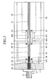
- FIG. 3
- is a partially cutout plan view of a connection structure between a coaxial
connector and a multilayer board in accordance with a second embodiment of
the present invention.
- FIG. 4
- is a partially cutout plan view of a connection structure between a coaxial
connector and a multilayer board in accordance with a third embodiment of the
present invention.
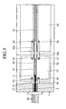
- FIG. 5
- is a partially cutout plan view of a connection structure between a coaxial
connector and a multilayer board, in accordance with a fourth embodiment of
the present invention.
- FIG. 6
- is a partially cutout plan view of a connection structure between a coaxial
connector and a multilayer board in accordance with a fifth embodiment of the
present invention.
BEST MODE FOR CARRYING OUT THE INVENTION
An embodiment of the present invention will now be described with reference to the
drawings in order to make description in further detail of the present invention.
EMBODIMENT 1
FIG. 1 is a longitudinal sectional side view of a connection structure between a coaxial
connector and a multilayer board in accordance with a first embodiment of the present
invention, and FIG. 2 is a partially cutout plan view of FIG. 1.
As shown in FIG. 1 and FIG. 2, a coaxial connector 10 and a multilayer board (high-frequency
board) 20 are mounted on an electroconductive casing 1, and a transfer or
intermediate board 30 electrically connecting the both is disposed between the coaxial
connector 10 and the multilayer board 20.
To explain in further detail, a connector-mounting hole 2 is prepared at the sidewall of
the casing 1, and the core wire 11 of the coaxial connector 10 is inserted into this
connector-mounting hole 2 through an insulator 12. Moreover, the transfer board 30 is
mounted on the inner wall of the casing 1. The transfer board 30 is constructed of a
double-sided board on the top surface of which a signal line pattern 31 composing a
microstripline-type transmission line is formed and on the bottom surface of which the
ground pattern of a microstripline-type transmission line (hereinafter, referred to as
'ground pattern') 32 is formed, and in the vicinity of the one end side of the transfer
board (in the vicinity of the end portion of the board that is opposite to the connector-mounting
hole 2), a via hole 33 that electrically connects the top surface layer of the
board and the ground pattern 32 is provided. Here, the core wire 11 of the coaxial
connector 10 inserted in the connector-mounting hole 2, as mentioned above, extends
to the upper portion of the signal line pattern 31 of the transfer board 30 mounted on
the inner wall of the casing 1, and is electrically connected to the signal line pattern 31
with a brazing material such as solder.
Further, the multilayer board 20 is mounted on the inner wall of the casing 1 so as to
be adjacent to the transfer board 30 on the side of the wall that is opposite to the
connector-mounting hole 2. The multilayer board 20 has a signal line pattern 21
constituting a microstripline-type transmission line located on the top surface thereof,
the ground pattern 22 of the microstripline transmission line located on the board-internal
layer (hereinafter, referred to as 'board-internal-layer ground pattern'), and a
board-bottom-surface ground pattern 23; and further, the multilayer board has a via
hole 24 that electrically interconnects these patterns 22, 23 and the top surface of the
board at one place near the transfer board 30.
Furthermore, on the top surfaces on the neighboring sides of the multilayer board 20
and the transfer board 30, the signal line patterns 21 and 31 of both the boards are
electrically connected each other by means of ribbon bonding or the like. Similarly,
the via holes 24 and 33 are mutually electrically connected by means of ribbon
bonding or the like. In such a way, a transmission line is formed such that the signal
line pattern 31 of the transfer board 30 and the signal line pattern 21 located on the top
surface of the multilayer board 20, and the ground patterns 22, 23, and 32 are
electrically connected by coplanar- type transmission lines 40, 40a. Briefly, this
transmission line constructs a high-frequency transmission line that is continuous by
extending across the transfer board 30 and the multilayer board 20.
The operation will now be described as below.
A high frequency signal input from the coaxial connector 10 passes the connecting
portion between the core wire 11 of the coaxial connector 10 and the signal line
pattern 31 of the transfer board 30, propagates through the microstripline-type
transmission line 31 constructed of the above-described signal line pattern, then passes
the coplanar-type transmission line 40, and subsequently propagates through the
microstripline-type transmission line 21 constructed of the signal line pattern formed
on the multilayer board 20. Also in the case of the propagating line in the opposite
direction thereto, the high frequency signal, which has propagated through the
microstripline-type transmission line constructed of the signal line pattern 21 formed
on the top surface of the multilayer board 20, passes the coplanar-type transmission
line 40, then propagates through the microstripline-type transmission line constructed
of the signal line pattern 31 formed on the transfer board 30, passes the connection
between the core wire 11 of the coaxial connector 10 and the signal line pattern 31
formed on the transfer board 30, and propagates to the coaxial connector 10.
According to the first embodiment described above, it is arranged as follows: the
transfer board 30 is disposed between the multilayer board 20 mounted in the
electroconductive casing 1 and the coaxial connector 10; the signal line pattern 31
formed on the transfer board 30 and the core wire 11 of the coaxial connector 10 are
electrically connected; and further, the signal line pattern 31 formed on the transfer
board 30 and the signal line pattern 21 formed on the tope surface of the multilayer
board 20 are electrically connected by the coplanar-type transmission line 40. As a
result, there is an effect that the disorder of impedance can be greatly reduced, and an
excellent return-loss characteristic can be ensured over a broad band.
In other words, according to the above first embodiment, the disorder of impedance
may be caused in the electrical connection between the coaxial connector 10 and the
transfer board 30; however, in contrast to the circuit on the multilayer board 20, a
control system circuit does not need to be mounted on the transfer board 30. This
enables the transfer board 30 to have an optimum board structure and design.
Therefore, the thickness of the transfer board 30 can be extremely reduced. This can
place the signal line pattern 31 formed on the top surface of the transfer board 30
much closer to the ground pattern 32 formed on the bottom surface thereof, and can
also place the grounding face formed on the casing much closer to the core wire 11 of
the coaxial connector in comparison with the structure in which the multilayer board
20 is electrically directly connected to the coaxial connector 10. Consequently, there is
an effect that in this area the disorder of impedance of the transmission line is greatly
improved.
In addition, in the multilayer board 20, it is difficult to form the inner-layer ground
pattern 22 of the microstripline-type transmission line to be close to the end face of the
board, where the ground pattern 22 is constructed of the signal line pattern 21 formed
on the uppermost layer thereof and the inner-layer ground pattern 22 located
immediately under the line pattern 21. For this reason, there exists a pattern margin
M1 (see FIG. 1 and FIG. 2) between the end face of the inner-layer ground pattern 22
and the end face of the board. However, the transfer board 30 is constructed of a
single-layered, double-sided board, not a multilayer board. Therefore, the employment
of, for example, an alumina substrate as the transfer board 30 enables the great
reduction of the pattern margin M2 between the end face of the ground pattern 32
formed on the bottom surface of the substrate and the end face to the substrate. Briefly,
in the transfer board 30, it is possible to form the ground pattern 32 located on the
bottom surface thereof closely to the end face of the board. For this reason, there is an
effect that the disorder of impedance of the transmission line in the vicinity of the end
face of the board caused in the multilayer board 20 can be greatly reduced. As a result,
there is an effect that an excellent return-loss characteristic over a broad band can be
obtained by the above-described connection or joining between the coaxial connector
10 and the transfer board 30.
In contrast, if it is arranged that the signal line patterns 21, 31 forming the
microstripline-type transmission line that is common to the surfaces of the multilayer
board 20 and of the transfer board 30 are connected to each other, so that the two
boards 20, 30 may be connected to each other, the pattern margin M1 of the internal
layer of the multilayer board 20, the thickness of the multilayer board 20, and the
thickness of the wall of the board gap become large. In this case, the impedance is
greatly disordered in the connected portion between both the boards 20 and 30, and the
excellent return-loss characteristic cannot be obtained.
However, according to the above first embodiment, the signal line pattern 31 formed
on the transfer board 30 and the signal line pattern 21 formed on the top surface of the
multilayer board 20 are connected by the coplanar-type transmission line 40 formed by
means of ribbon bonding or the like. Thereby, the electromagnetic field in the
connection propagates through the coplanar-type transmission line 40 to be
concentrated on the transmission line only, thereby greatly reducing the distribution of
the electromagnetic field in an inward direction of the board. Therefore, the influence
of the disorder of impedance is hardly received, which may be caused by the
transmission line in the vicinity of the end face of the multilayer board 20, depending
on the presence or absence of the internal-layer ground pattern 22 of the board
multilayer 20, the thickness of the wall of the board gap, and the thickness of the
multilayer board 20. For this reason, there is an effect that a favorable return-loss
characteristic can be obtained over a broad band in the electrical connection between
the above-described transfer board 30 and the multilayer board 20 as well. As a result,
there is an effect that a favorable return-loss characteristic can be obtained over a
broad band in the entire transmission line extending from the coaxial connector 10 to
the transfer board 30 and the multilayer board 20 as well.
EMBODIMENT 2
FIG. 3 is a partially cutout plan view of a connection structure between a coaxial
connector and a multilayer board according to a second embodiment of the present
invention. The same or equivalent parts as the ones in FIG. 1 and FIG. 2 are designated
by similar numerals to omit the repetitive explanation.
In the second embodiment, in the connection structure between the coaxial connector
and the multilayer board according to the above first embodiment, it is arranged such
that also in the vicinity of the end face of the transfer board 30 on the side of the
coaxial connector 10, two coaxial-connector-to-transfer-board via holes 34 are
provided, thereby electrically connecting the via holes 34 and the electroconductive
casing 1 by use of two transfer-board-connecting lines 41 formed by means of ribbon
bonding or the like.
According to the second embodiment of such a structure, a coplanar-type transmission
line is constructed by using the two coaxial-connector-to-transfer-board connecting
lines 41, which are electrically connected from the two coaxial-connector-to-transfer-board
via holes 34 to the electroconductive casing 1, and the core wire 11 of the
coaxial connectors 10. As a result, the disorder of impedance can be suppressed still
more effectively as compared to the case that performs the electrical connection
between the coaxial connector 10 and the transfer board 30 by only the core wire 11 of
the coaxial connector 10. Therefore, there is an effect that the return-loss characteristic
can be further improved as compared to the case in the above-mentioned first
embodiment.
EMBODIMENT 3
FIG. 4 is a partially cutout plan view of a connection structure between a coaxial
connector and a multilayer board according to a third embodiment of the present
invention. The same parts as the ones in FIG. 3 are designated by similar numerals to
omit the repetitive explanation.
In the third embodiment, in the connection structure between the coaxial connector and
the multilayer board according to the second embodiment, it is arranged that a
coplanar-type transmission line 35 is formed on the top surface of the transfer board
30 instead of the microstripline.
Thus, according to the above third embodiment, the connection structure is arranged so
that the top surface of the transfer board 30 is provided with the coplanar-type
transmission line 35. Accordingly, the coplanar-type transmission line is constructed of
two coaxial-connector-to-transfer-board connecting lines 41, which are connected from
the coaxial-connector-to-transfer-board via holes 34 to the electroconductive casing 1,
and the core wire 11 of the coaxial connector 10. Thereby, when the electromagnetic
wave is propagated from this coplanar-type transmission line to the transfer board 30,
and also when the electromagnetic wave is propagated in the opposite direction
thereof, in either case, the propagation thereof can be always performed while keeping
up the electromagnetic-field-transmission mode of the coplanar type. For this reason,
there is an effect that the deterioration of the return-loss characteristic can be
suppressed more effectively as compared to the case in the formation of the
microstripline-type transmission line on the top surface of the transfer board 30, which
needs the conversion of the electromagnetic-field-transmission mode between the
microstripline type and the coplanar type. Similarly, when the electromagnetic wave is
propagated from the transfer board 30 to the coplanar-type transmission line 40, or
also when the electromagnetic wave is propagated in the opposite direction, the
propagation thereof can be always performed while keeping up the electromagnetic-field-transmission
mode of the coplanar type. Accordingly, there is an effect that the
deterioration of the return-loss characteristic can be suppressed more positively as
compared to the case on the formation of only the microstripline-type transmission
line on the top surface of the transfer board 30, which needs the conversion of the
electromagnetic-field-transmission mode between the microstripline type and the
coplanar type. Consequently, there is an effect that the return-loss characteristic can be
improved more effectively in the third embodiment than in the above-mentioned
second embodiment.
EMBODIMENT 4
FIG. 5 is a partially cutout plan view of a connection structure between a coaxial
connector and a multilayer board according to a fourth embodiment of the present
invention. The same parts as the ones in FIG. 3 are designated by similar numerals to
omit the repetitive explanation.
In the above third embodiment, the coplanar-type transmission line 35 is substituted
for the microstripline-type transmission line 31 used on the transfer board 30 in the
above second embodiment; however, in the fourth embodiment, a coplanar-type
transmission line 25 is substituted for the microstripline-type transmission line 21 used
on the multilayer board 20 in the above second embodiment.
According to the fourth embodiment, it is arranged that the coplanar-type transmission
line 25 replacing the microstripline-type transmission line 21 according to the above
second embodiment be provided on the top surface of the multilayer board 20. Thus,
when the electromagnetic wave is propagated from the multilayer board 20 to the
coplanar-type transmission line 25, and also when the electromagnetic wave is
propagated in the opposite direction, in either case, the propagation thereof can be
always performed while keeping up the electromagnetic field transmission mode of the
coplanar type. Accordingly, there is an effect that the deterioration of the return-loss
characteristic can be suppressed more effectively as compared to the case on the
formation of the microstripline-type transmission line on the top surface of the
multilayer board 20, which needs the conversion of the electromagnetic-field-transmission
mode between the microstripline type and the coplanar type. Therefore,
there is an effect that the return-loss characteristic can be improved more effectively in
the fourth embodiment than in the above-mentioned second embodiment.
EMBODIMENT 5
FIG. 6 is a partially cutout plan view of a connection structure between a coaxial
connector and a multilayer board according to a fifth embodiment of the present
invention. The same parts as the ones in FIG. 3 are designated by similar numerals to
omit the repetitive explanation.
In the fifth embodiment, it is arranged that coplanar- type transmission lines 35 and 25
replacing the microstripline- type transmission lines 31 and 21 according to the above
second embodiment are formed on both the top surfaces of the transfer board 30 and
the multilayer board 20.
According to the fifth embodiment in which the coplanar- type transmission lines 35
and 25 are thus formed on both the top surfaces of the transfer board 30 and the
multilayer board 20, when the electromagnetic wave is propagated from the coplanar-type
transmission line, which is constructed of the two electroconductive-casing-to-transfer-board
connecting lines 41 connected from the coaxial-connector-to-transfer-board
via holes 34 to the electroconductive casing 1 and the core wire 11 of the
coaxial connector 10, to the transfer board 30, and also when the electromagnetic wave
is propagated in the opposite direction, in either case, the propagation thereof can be
always performed while keeping up the electromagnetic field transmission mode of the
coplanar type. For this reason, there is an effect that the deterioration of the return-loss
characteristic can be suppressed more positively as compared to the case that is formed
with the microstripline-type transmission line on the top surface of the transfer board
30 such that the conversion of the electromagnetic-field-transmission mode between
the microstripline type and the coplanar type is necessary.
Further, when the electromagnetic wave is propagated from the transfer board 30 to the
coplanar-type transmission line 40, and also when the electromagnetic wave is
propagated in the opposite direction, in either case, the propagation thereof can be
always performed while keeping up the electromagnetic-field-transmission mode of
the coplanar type. For this reason, there is an effect that the deterioration in the return
loss characteristic can be suppressed more positively as compared to the case that is
formed with the microstripline-type transmission line. Furthermore, when the
electromagnetic wave is propagated from the multilayer board 20 to the coplanar-type
transmission line 40, and also when the electromagnetic wave is propagated in the
opposite direction, in either case, the propagation thereof can be always performed
while keeping up the electromagnetic-field-transmission mode of the coplanar type.
Consequently, there is an effect that the deterioration of the return-loss characteristic
can be suppressed more effectively as compared to the case formed with the
microstripline-type transmission line on the top surface of the multilayer board 20
such that the conversion of the electromagnetic-field-transmission mode between the
microstripline type and the coplanar type is necessary. Therefore, there is an effect that
the return-loss characteristic can be improved more positively in the fifth embodiment
than in the above-mentioned second embodiment 2.
INDUSTRIAL APPLICABILITY
As mentioned above, a connection structure between a coaxial connector and a
multilayer board according to the present invention can be used for a high-frequency
circuits and so on of communication apparatuses.