EP1602972A1 - Method for manufacturing optical device - Google Patents
Method for manufacturing optical device Download PDFInfo
- Publication number
- EP1602972A1 EP1602972A1 EP04717772A EP04717772A EP1602972A1 EP 1602972 A1 EP1602972 A1 EP 1602972A1 EP 04717772 A EP04717772 A EP 04717772A EP 04717772 A EP04717772 A EP 04717772A EP 1602972 A1 EP1602972 A1 EP 1602972A1
- Authority
- EP
- European Patent Office
- Prior art keywords
- optical
- optical component
- positioning
- casing
- manufacturing
- Prior art date
- Legal status (The legal status is an assumption and is not a legal conclusion. Google has not performed a legal analysis and makes no representation as to the accuracy of the status listed.)
- Withdrawn
Links
Images























Classifications
-
- H—ELECTRICITY
- H04—ELECTRIC COMMUNICATION TECHNIQUE
- H04N—PICTORIAL COMMUNICATION, e.g. TELEVISION
- H04N9/00—Details of colour television systems
- H04N9/12—Picture reproducers
- H04N9/31—Projection devices for colour picture display, e.g. using electronic spatial light modulators [ESLM]
- H04N9/3141—Constructional details thereof
- H04N9/317—Convergence or focusing systems
-
- G—PHYSICS
- G03—PHOTOGRAPHY; CINEMATOGRAPHY; ANALOGOUS TECHNIQUES USING WAVES OTHER THAN OPTICAL WAVES; ELECTROGRAPHY; HOLOGRAPHY
- G03B—APPARATUS OR ARRANGEMENTS FOR TAKING PHOTOGRAPHS OR FOR PROJECTING OR VIEWING THEM; APPARATUS OR ARRANGEMENTS EMPLOYING ANALOGOUS TECHNIQUES USING WAVES OTHER THAN OPTICAL WAVES; ACCESSORIES THEREFOR
- G03B21/00—Projectors or projection-type viewers; Accessories therefor
- G03B21/14—Details
- G03B21/145—Housing details, e.g. position adjustments thereof
-
- G—PHYSICS
- G02—OPTICS
- G02B—OPTICAL ELEMENTS, SYSTEMS OR APPARATUS
- G02B27/00—Optical systems or apparatus not provided for by any of the groups G02B1/00 - G02B26/00, G02B30/00
- G02B27/10—Beam splitting or combining systems
- G02B27/1006—Beam splitting or combining systems for splitting or combining different wavelengths
- G02B27/1013—Beam splitting or combining systems for splitting or combining different wavelengths for colour or multispectral image sensors, e.g. splitting an image into monochromatic image components on respective sensors
-
- G—PHYSICS
- G02—OPTICS
- G02B—OPTICAL ELEMENTS, SYSTEMS OR APPARATUS
- G02B27/00—Optical systems or apparatus not provided for by any of the groups G02B1/00 - G02B26/00, G02B30/00
- G02B27/10—Beam splitting or combining systems
- G02B27/1006—Beam splitting or combining systems for splitting or combining different wavelengths
- G02B27/102—Beam splitting or combining systems for splitting or combining different wavelengths for generating a colour image from monochromatic image signal sources
-
- G—PHYSICS
- G02—OPTICS
- G02B—OPTICAL ELEMENTS, SYSTEMS OR APPARATUS
- G02B27/00—Optical systems or apparatus not provided for by any of the groups G02B1/00 - G02B26/00, G02B30/00
- G02B27/10—Beam splitting or combining systems
- G02B27/1006—Beam splitting or combining systems for splitting or combining different wavelengths
- G02B27/102—Beam splitting or combining systems for splitting or combining different wavelengths for generating a colour image from monochromatic image signal sources
- G02B27/1046—Beam splitting or combining systems for splitting or combining different wavelengths for generating a colour image from monochromatic image signal sources for use with transmissive spatial light modulators
-
- G—PHYSICS
- G02—OPTICS
- G02B—OPTICAL ELEMENTS, SYSTEMS OR APPARATUS
- G02B27/00—Optical systems or apparatus not provided for by any of the groups G02B1/00 - G02B26/00, G02B30/00
- G02B27/10—Beam splitting or combining systems
- G02B27/1073—Beam splitting or combining systems characterized by manufacturing or alignment methods
-
- G—PHYSICS
- G02—OPTICS
- G02B—OPTICAL ELEMENTS, SYSTEMS OR APPARATUS
- G02B27/00—Optical systems or apparatus not provided for by any of the groups G02B1/00 - G02B26/00, G02B30/00
- G02B27/10—Beam splitting or combining systems
- G02B27/14—Beam splitting or combining systems operating by reflection only
- G02B27/145—Beam splitting or combining systems operating by reflection only having sequential partially reflecting surfaces
-
- G—PHYSICS
- G02—OPTICS
- G02B—OPTICAL ELEMENTS, SYSTEMS OR APPARATUS
- G02B27/00—Optical systems or apparatus not provided for by any of the groups G02B1/00 - G02B26/00, G02B30/00
- G02B27/10—Beam splitting or combining systems
- G02B27/14—Beam splitting or combining systems operating by reflection only
- G02B27/149—Beam splitting or combining systems operating by reflection only using crossed beamsplitting surfaces, e.g. cross-dichroic cubes or X-cubes
-
- G—PHYSICS
- G02—OPTICS
- G02B—OPTICAL ELEMENTS, SYSTEMS OR APPARATUS
- G02B27/00—Optical systems or apparatus not provided for by any of the groups G02B1/00 - G02B26/00, G02B30/00
- G02B27/62—Optical apparatus specially adapted for adjusting optical elements during the assembly of optical systems
-
- G—PHYSICS
- G02—OPTICS
- G02B—OPTICAL ELEMENTS, SYSTEMS OR APPARATUS
- G02B7/00—Mountings, adjusting means, or light-tight connections, for optical elements
- G02B7/003—Alignment of optical elements
-
- H—ELECTRICITY
- H04—ELECTRIC COMMUNICATION TECHNIQUE
- H04N—PICTORIAL COMMUNICATION, e.g. TELEVISION
- H04N9/00—Details of colour television systems
- H04N9/12—Picture reproducers
- H04N9/31—Projection devices for colour picture display, e.g. using electronic spatial light modulators [ESLM]
- H04N9/3102—Projection devices for colour picture display, e.g. using electronic spatial light modulators [ESLM] using two-dimensional electronic spatial light modulators
- H04N9/3105—Projection devices for colour picture display, e.g. using electronic spatial light modulators [ESLM] using two-dimensional electronic spatial light modulators for displaying all colours simultaneously, e.g. by using two or more electronic spatial light modulators
-
- G—PHYSICS
- G03—PHOTOGRAPHY; CINEMATOGRAPHY; ANALOGOUS TECHNIQUES USING WAVES OTHER THAN OPTICAL WAVES; ELECTROGRAPHY; HOLOGRAPHY
- G03B—APPARATUS OR ARRANGEMENTS FOR TAKING PHOTOGRAPHS OR FOR PROJECTING OR VIEWING THEM; APPARATUS OR ARRANGEMENTS EMPLOYING ANALOGOUS TECHNIQUES USING WAVES OTHER THAN OPTICAL WAVES; ACCESSORIES THEREFOR
- G03B2217/00—Details of cameras or camera bodies; Accessories therefor
- G03B2217/002—Details of arrangement of components in or on camera body
Definitions
- the present invention relates to a method for manufacturing an optical device.
- the projector includes an optical device that mainly consists of: optical components such as a lens for superposing the light beam irradiated by the light source on an image formation area of the optical modulator, a dichroic mirror for separating the light beam irradiated by the light source into three color lights (R, G and B) and a reflection mirror for conducting the light beam irradiated by the light source to the optical modulator; and an optical component casing, in which the optical components are housed and arranged at predetermined positions on an illumination optical axis of the light beam irradiated by the light source.
- optical components such as a lens for superposing the light beam irradiated by the light source on an image formation area of the optical modulator, a dichroic mirror for separating the light beam irradiated by the light source into three color lights (R, G and B) and a reflection mirror for conducting the light beam irradiated by the light source to the optical modulator; and an optical component casing, in which the optical components are
- the optical component casing is a synthetic resin molding product which is manufactured by molding such as injection molding with grooves formed on an inner side thereof to respectively engage with the optical components.
- Such optical device is so manufactured that the respective optical components are slid from an upper side of the optical component casing to be housed and arranged therein to engage with the grooves of the optical component casing.
- the grooves formed on the inner side of the optical component casing serve as external position reference of the optical component casing.
- the optical component can easily be housed and arranged in the optical component casing
- the groove formed on the inner side of the optical component casing requires to be formed in a highly accurate manner.
- a molding die for the optical component casing needs to be a complicated profile and to be highly accurately manufactured, the production cost of the optical component casing may be increased, and consequently, the production cost of the optical device may be increased.
- An object of the present invention is to provide a method for manufacturing an optical device that can reduce the production cost and can easily be manufactured.
- a method for manufacturing an optical device that includes a plurality of optical components arranged on an optical path of a light beam irradiated by a light source and an optical component casing with an illumination optical axis of the light beam being set therein, in which the optical components are housed and arranged at predetermined positions on the illumination optical axis, in which the optical component casing includes a casing body having a plurality of holes penetrating toward the inside, in which the plurality of optical components are housed and arranged therein, and a plurality of positioning members for positioning the plurality of optical components at the predetermined positions in the casing body, the method includes: an optical component housing operation for housing the plurality of optical components in the casing body; an optical component positioning operation for shifting the optical components to adjust the positions of the optical components, and positioning the optical components at the predetermined positions on the illumination optical axis of the light beam irradiated by the light source by the positioning members; and an optical component position fixing operation for fixing the positions of the optical components on
- the casing body of the optical component casing may be any profile as long as the plurality of optical components can be housed and arranged therein.
- the casing body may be a container structure or a hollow structure.
- the casing body may be a synthetic resin molding product manufactured by molding such as injection molding in the same manner as the conventional art, a structure formed by sheet metal processing, or a structure formed by BMC (Bulk Molding Compound).
- the method for manufacturing the optical device includes the optical component housing operation, the optical component positioning operation and the optical component position fixing operation.
- the plurality of optical components are housed in the casing body in the optical component housing operation, and the optical components are shifted so that the positions of the optical components are adjusted to be positioned in the casing body by the positioning members in the optical component positioning operation. After the optical components are positioned, the positions of the optical components are fixed in the casing body.
- the optical device can easily be manufactured.
- the manufacturing accuracy of the optical component casing need not to be so high as compared to an optical component casing having external position reference faces therein and being required to be highly accurately manufactured. Accordingly, the production cost of the optical component casing can be reduced, and consequently, the production cost of the optical device can be reduced.
- the optical component housing operation further includes the positioning member inserting process, the optical component housing process, and the positioning member abutting process. Since the positioning member is placed in the casing body together with the optical component after the positions of the optical components are adjusted by shifting, the optical components can easily and promptly be positioned by the positioning members in the optical component positioning operation.
- the optical component position fixing operation when the optical component is fixed on the casing body together with the positioning member, the optical component can be held by the positioning member, a member such as a holder frame for holding the optical component can be omitted, and the production cost can further be reduced when the optical device is manufactured.
- the positioning member in the above method for manufacturing the optical device, in the positioning member abutting process, the positioning member abuts on the optical component arranged along an inner side of the casing body.
- the optical component arranged along the inner side of the casing body is a full reflection mirror for conducting the light beam irradiated by the light source to a predetermined position.
- the positioning member abuts on a back side of the optical component such as the full reflection mirror or the end of the optical component such as the full reflection mirror. Accordingly, in the optical component positioning operation, the positioning member can easily and promptly position the optical component after the position of the optical component is adjusted by the optical component such as the full reflection mirror.
- the optical component position fixing operation when the optical component is fixed on the casing body together with the positioning member, the optical component such as the full reflection mirror can be held by the positioning member while the positioning member can be arranged at the position not interfering with the light beam irradiated by the light source, thus manufacturing the optical device that forms a fine optical image.
- the positioning member includes a plate body and a plurality of pins projected on an end of the plate body, in the positioning member inserting process, the plurality of pins are inserted to the plurality of holes, in the positioning member abutting process, tip ends of the plurality of inserted pins abut on the optical component, and in the optical component positioning operation, the optical component abutting on the plurality of pins is shifted by shifting the plate body to adjust the position of the optical component, and the optical component is positioned at the predetermined position on the illumination optical axis of the light beam irradiated by the light source.
- the positioning member has the plate body and the plurality of pins.
- the plurality of pins of the positioning member are inserted to the plurality of holes formed on the casing body.
- the plurality of inserted pins abut on the optical component such as the full reflection mirror.
- the optical component positioning process the optical component abutting on the plurality of pins is shifted by shifting the plate body so that the position of the optical component is adjusted, and the optical component is positioned at the predetermined position by the positioning member. Accordingly, the plurality of pins can be shifted at once by shifting the plate body as compared to, for example, that the optical component is positioned by shifting the plurality of pins one by one, thus easily and promptly positioning the optical component such as the full reflection mirror.
- the positioning member in the above method for manufacturing the optical device, in the positioning member abutting process, the positioning member abuts on the optical component to be housed in the casing body in a manner orthogonal to the illumination optical axis of the light beam irradiated by the light source.
- the optical component housed in the casing body to be orthogonal to the illumination optical axis of the light beam irradiated by the light source may be a light beam separating optical element for separating the light beam irradiated by the light source, a focusing optical element for focusing the light beam irradiated by the light source at a predetermined position, or the like.
- the positioning member is placed on the casing body together with the optical component in the optical component housing operation, while the positioning member abuts on the outer periphery of the optical component such as the light beam separating optical element or the focusing optical element in the positioning member abutting process of the optical component housing operation. Accordingly, in the optical component positioning operation, the optical component can easily and promptly be positioned by the positioning member after the optical component such as the light beam separating optical element or the focusing optical element is shifted for adjusting the position thereof.
- the positioning member has a groove having a V-shaped cross section, and in the positioning member abutting process, the groove of the positioning member abuts on an outer periphery of the optical component.
- the positioning member has the groove having an approximately V-shaped cross-section. Since the groove abuts on the outer periphery of the optical component such as the light beam separating optical element or the focusing optical element in the positioning member abutting process of the optical component housing operation, the optical component such as the light beam separating optical element or the focusing optical element can accurately be positioned by the positioning member in the optical component positioning operation.
- the position of the optical component such as the light beam separating optical element or the focusing optical element can securely be fixed by the positioning member.
- a support face is formed on a periphery of the hole and is extended toward the inside of the casing body, and in the positioning member inserting process, the positioning member is inserted to the hole so that the support face supports the positioning member.
- the positioning member in the positioning member inserting process, the positioning member is inserted to the hole formed on the casing body while the positioning member is supported by the support face formed on the periphery of the hole, thus accurately positioning the optical component by the positioning member in the optical component positioning operation.
- the position of the optical component can further securely be fixed by the positioning member and the support face for supporting the positioning member.
- the optical component casing includes a rework member that is mountable on an outer side of the casing body and is provided with a screw member and a support member having a hole to which the screw member is inserted, the support member abutting on the outer side of the casing body, the positioning member has a screw configuration screwing with the screw member, and after the optical component position fixing operation, a rework operation is provided in which the support member abuts on a position corresponding to the hole of the casing body and the screwing state between the screw member and the screw configuration is changed to shift the positioning member, so that the fixing state of the optical component is released from the casing body.
- the optical component casing includes the rework member having the screw member and the support member, and capable of being mounted on the outer side of the casing body.
- the positioning member has a screwing configuration that can screw with the screw member of the rework member.
- the casing body has a pair of plate members oppositely arranged, the positioning member has a spacer interposed between the members, and the optical component housing operation includes a spacer placing process for placing the spacer on the plate member, an optical component arranging process for arranging the optical component so that ends of the optical component oppose to the pair of plate members, and a spacer abutting process for abutting the spacer to the end of the optical component.
- optical component arranged in the above-described optical component arranging process is preferably an optical component housed in an inclined manner relative to the inner side of the casing body.
- optical component may be a color-separating optical element for separating the light beam irradiated by the light source into a plurality of color lights.
- the lateral side of the casing body may serve as the pair of plate members, or a member other than the lateral side of the casing body may serve as the pair of plate members.
- the optical component housing operation includes the spacer placing process, the optical component arranging process, and the spacer abutting process. Since the spacers of the positioning member are placed on the plate member together with the optical component such as the color-separating optical element, the optical component such as the color-separating optical element can easily and promptly be positioned after the optical component is shifted for adjusting the position thereof.
- the optical component position fixing operation when the optical component is fixed on the casing body together with the spacers, the optical component can be held by the spacers, a member such as a holder frame for holding the optical component such as the color-separating optical element can be omitted, and the production cost can further be reduced when the optical device is manufactured.
- the pair of plate members are composed of the lateral side of the casing body.
- the pair of plate members are composed of the lateral side of the casing body, when the optical device is manufactured, an operation for placing the pair of plate members in the casing body can be omitted, thus easily and promptly manufacturing the optical device.
- the positioning member includes the spacer, a mount fixed on a bottom side of the casing body, and the pair of plate members vertically provided on the mount, in the spacer placing process, the spacer is placed on the pair of plate members, and in the optical component arranging process, the optical component is arranged so that the ends of the optical component oppose to the pair of plate members.
- the optical component is arranged on the positioning member.
- the positioning member on which the optical component is arranged is housed in the casing body, accordingly, the optical component can easily be housed without a cumbersome work of housing the optical component such as the color-separating optical element in the casing body with the various optical components being closely arranged, in an inclined manner relative to the lateral side of the casing body, thus easily manufacturing the optical device.
- the positioning member since the lateral side of the casing body does not serve as the plate members, but the positioning member includes the plate member, even when the profile of the optical component such as the color-separating optical element is changed, the profile of the casing body is not necessary to be changed, and the plate members of the positioning member can correspond by changing the adjacent distance thereof.
- support faces are formed on the pair of plate members and are extended toward the other plate member, and in the spacer placing process, the spacer is placed on the support face.
- the optical component can accurately be positioned by the spacer in the optical component positioning operation.
- the position of the optical component can securely be fixed by the spacer and the support face for supporting the spacer.
- the spacer has a slanted face slanted along an inclined direction of the optical component, and in the spacer abutting process, the slanted face of the spacer abuts on the end of the optical component.
- the spacer in the spacer abutting process, since the slanted face of the spacer abuts on the end of the optical component, the spacer can securely abut on the optical component, so that the optical component can accurately be positioned by the spacer in the optical component positioning operation.
- the position of the optical component can securely be fixed by the spacer.
- the optical component casing includes a rework member that is mountable on an outer side of the casing body and is provided with a screw member and a support member having a hole to which the screw member is inserted, the support member abutting on the outer side of the casing body, the spacer has a screw configuration screwing with the screw member, and after the optical component position fixing operation, a rework operation is provided in which the support member abuts on a position corresponding to the spacer of the plate member and the screwing state between the screw member and the screw configuration is changed to shift the spacer, so that the fixing state of the optical component is released from the plate member.
- the optical component casing includes the rework member having the screw member and the support member, and capable of being mounted on the plate member.
- the spacer of the positioning member has a screwing configuration that can screw with the screw member of the rework member.
- an adhesive is filled between the optical component and the positioning member and also between the positioning member and the casing body, the optical component positioning operation is performed with the adhesive not being cured, and in the optical component position fixing operation, after the optical component is positioned in the optical component positioning operation, the adhesive is cured so that the position of the optical component is fixed on the casing body together with the positioning member.
- the optical component is positioned with the adhesive filled between the optical component and the positioning member, and also between the positioning member and the casing body. Further, in the optical component position fixing operation, the position of the optical component is fixed on the casing body by the filled adhesive being cured. Accordingly, the position of the optical component can easily be fixed on the casing body.
- the adhesive is a light curing adhesive
- the positioning member is a light transmissive component
- a light beam is irradiated on the light curing adhesive through the positioning member to cure the light curing adhesive so that the position of the optical component is fixed on the casing body together with the positioning member.
- synthetic resin such as acrylic material, sapphire glass, crystal, quarts and fluorite can be applied for the light-transmissive component.
- the light curing adhesive is used for fixing the position of the optical component on the casing body, and the positioning member is made of the light-transmissive component.
- the light beam is irradiated between the members via the positioning member to cure the light curing adhesive. Accordingly, the light curing adhesive can easily and securely be cured.
- the position of the optical component can easily and securely be fixed at the optimum position.
- a method for manufacturing an optical device that includes a plurality of optical components arranged on an optical path of a light beam irradiated by a light source and an optical component casing with an illumination optical axis of the light beam being set therein, in which the optical components are housed and arranged at predetermined positions on the illumination optical axis, in which at least one opening penetrating toward the inside is formed on the optical component casing, the method includes: a casing placing operation for placing the optical component casing at a predetermined position so that a part of a positioning jig is inserted to the opening; an optical component positioning operation for housing the plurality of optical components inside the optical component casing through the opening of the optical component casing and positioning at the designed predetermined positions with the use of the positioning jig inserted to the opening; and an optical component position fixing operation for fixing the positions of the plurality of optical components positioned in the optical component positioning operation on the optical component casing.
- the optical component casing may be any profile as long as the plurality of optical components can be housed and arranged therein.
- the optical component casing may be a container structure or a hollow structure in the same manner as the casing body.
- the optical component casing may be a synthetic resin molding product manufactured by molding such as injection molding, a structure formed by sheet metal processing, or a structure formed by BMC.
- the optical component casing includes at least one opening penetrating toward the inside.
- the optical component casing is shifted in the casing placing operation so that the part of the positioning jig is inserted to the opening formed on the optical component casing to place the optical component casing at the predetermined position.
- the plurality of optical components are shifted to be housed in the optical component casing via the opening of the optical component casing in the optical component positioning operation, so that the plurality of optical components are positioned at the designed predetermined positions by the positioning jig inserted to the opening of the optical component casing. Thereafter, the positions of the plurality of optical components are fixed on the optical component casing in the optical component position fixing operation.
- the optical device can easily be manufactured.
- the manufacturing accuracy of the optical component casing need not to be so high as compared to an optical component casing having external position reference faces therein and being required to be highly accurately manufactured. Accordingly, the production cost of the optical component casing can be reduced, and consequently, the production cost of the optical device can be reduced.
- the optical component can be prevented from the displacement caused by the optical component casing interfering against the positioned optical component in the casing placing operation.
- a method for manufacturing an optical device that includes a plurality of optical components arranged on an optical path of a light beam irradiated by a light source and an optical component casing with an illumination optical axis of the light beam being set therein, in which the optical components are housed and arranged at predetermined positions on the illumination optical axis, in which at least one opening penetrating toward the inside is formed on the optical component casing, the method includes: an optical component positioning operation for positioning the plurality of optical components at the designed predetermined positions with the use of the positioning jig; a casing placing operation for placing the optical component casing on a predetermined position corresponding to the plurality of optical components so that the plurality of optical components positioned in the optical component positioning operation are housed therein through the opening; and an optical component position fixing operation for fixing the positions of the plurality of optical components positioned in the optical component positioning operation on the optical component casing.
- the optical component casing may be any profile as long as the plurality of optical components can be housed and arranged therein.
- the optical component casing may be a container structure or a hollow structure in the same manner as the above-described optical component casing.
- the optical component casing may be a synthetic resin molding product manufactured by molding such as injection molding, a structure formed by sheet metal processing, or a structure formed by BMC.
- the plurality of optical components are positioned at the designed predetermined positions by the positioning jigs in the optical component positioning operation. Further, in the casing placing operation, the optical component casing is shifted so that the plurality of optical components positioned through the opening of the optical component casing is inserted to the inside to place the optical component casing at the predetermined position corresponding to the plurality of optical components. Thereafter, the positions of the plurality of optical components are fixed on the optical component casing in the optical component position fixing operation.
- the optical device can easily be manufactured.
- the manufacturing accuracy of the optical component casing need not to be so high as compared to an optical component casing being required to be highly accurately manufactured. Furthermore, the optical component casing only requires to have at least one opening. Accordingly, the production cost of the optical component casing can further be reduced, and consequently, the production cost of the optical device can further be reduced.
- the optical component positioning operation includes an optical component supporting process for supporting the plurality of optical components on the designed predetermined positions with the use of the positioning jig, an optical image detecting process for irradiating the light beam on the plurality of optical components supported in the optical component supporting process to detect an optical image via the plurality of optical components by an optical image detecting device, and an optical component position adjusting process for adjusting the position of at least any of the plurality of optical components by operating the positioning jig based on the optical image detected in the optical image detecting process.
- the optical image detecting device may be, for instance, that directly detects the optical image via the plurality of optical components, or that projects the optical image via the plurality of optical components on the screen in an enlarged manner to detect the optical image projected on the screen.
- the optical image detecting device may employ, for example, an image pickup element such as a CCD (Charge Coupled Device) and a MOS (Metal Oxide Semiconductor) sensor etc.
- the optical component positioning operation includes the optical component supporting process
- the plurality of optical components can easily be positioned at the designed predetermined positions with the plurality of optical components being supported by the positioning jig.
- the optical component positioning operation includes the optical image detecting process, it can be determined whether or not the plurality of optical components are positioned at the designed predetermined positions according to the optical image detected in the optical image detecting process.
- the optical component positioning operation includes the optical component position adjusting process, when the plurality of optical components are not positioned at the designed predetermined positions, or when there are the optical components requiring the adjustment in the plurality of optical components, the positions of the optical components can be adjusted by operating the positioning jig according to the optical image detected in the optical image detecting process.
- the optical components are highly accurately positioned.
- the positioning jig is controllably driven by a jig driver for driving the positioning jig, and by a controlling unit for controlling the jig driver
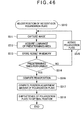
- the optical component position adjusting process includes an image capturing step for capturing the optical image detected in the optical image detecting process by the controlling unit to convert into an image signal, a luminance acquiring step for acquiring a luminance value by the controlling unit from the image signal converted in the image capturing step, a position adjustment amount computing step for computing a position adjustment amount of the optical component by the controlling unit based on the luminance value acquired in the luminance acquiring step, and a position adjusting step for adjusting the position of the optical component by driving the positioning jig under the control of the controlling unit based on the position adjustment amount computed in the position adjustment amount computing step.
- the controlling unit may be, for instance, a PC (Personal Computer) that includes a CPU (Central Processing Unit) reading and executing a control program, a video capture board inputting a signal output from the optical image detecting device to c6nvert into an image signal, and the like. Further, each step in the optical component position adjusting process can be configured as a program to be executed by the controlling unit.
- PC Personal Computer
- CPU Central Processing Unit
- the optical component position adjusting process includes the image capturing step, the luminance acquiring step, the position adjustment amount computing step and the position adjusting step so that the position of the optical component is adjusted with the drive control of the positioning jig by the controlling unit. Accordingly, the optical components can further accurately be positioned as compared to the case that the positions of the optical components are adjusted by manually operating the positioning jig with the optical image detected by the optical image detecting device being checked with eyes.
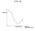
- the optical component position adjusting process includes an illumination area shifting step for shifting the optical component by driving the positioning jig under the control of the controlling unit and shifting the illumination area of the optical image via the optical component, and a boundary point acquiring step for acquiring a boundary point of the illumination area shifted in the illumination area shifting step by the controlling unit based on the luminance value acquired in the luminance acquiring step, and in the position adjustment amount computing step, the position adjustment amount of the optical component is computed by the controlling unit based on the boundary point of the illumination area acquired in the boundary point acquiring step.
- the optical component position adjusting process includes the illumination area shifting step and the boundary point acquiring step in addition to the image capturing step, the luminance acquiring step, the position adjustment amount computing step and the position adjusting step. Then, in the position adjustment amount computing step, the controlling unit computes the position adjustment amount of the optical component based on the boundary point of the illumination are acquired in the boundary point acquiring step. With this step, the displacement of the relative positions of the plural optical components can easily be recognized by the acquisition of the boundary position of the illumination area, thus enabling highly accurate positioning of the optical components.
- the optical component casing includes a support portion abutting on the optical component, an adhesive is filled between the optical component and the support portion, and in the optical component position fixing operation, the adhesive is cured to fix the position of the optical component on the optical component casing.
- the adhesive can be applied thereto in advance in the optical component positioning operation, or can be applied thereto after the optical component positioning operation and the casing placing operation are completed.
- the support portion can have a lateral side constituting the optical component casing, or can be a component independent from the lateral side constituting the optical component casing.
- the position of the optical component in the optical component position fixing operation, since the position of the optical component is fixed on the optical component casing by curing the adhesive applied between the optical component and the support portion, the position of the optical component can easily and promptly be fixed after positioning.
- a groove is formed on an abutting face of the support portion, which abuts on the optical component, and in the optical component position fixing operation, the adhesive is injected to the groove to fill the adhesive between the optical component and the support portion, and the adhesive is cured to fix the position of the optical component on the optical component casing.
- the groove may penetrate through the support portion from the first end to the opposing second end.
- the groove may be formed from the first end of the support portion to the part around the opposing second end thereof, in other words, the groove may be formed so as not to penetrate through the support portion from the first end to the opposing second end.
- the adhesive is injected to the groove to fill the adhesive between the optical component and the support portion.
- the adhesive is then cured, so that the position of the optical component is fixed on the optical component casing. Accordingly, the adhesive can easily be applied (injected) between the optical component and the support portion, thus further easily and promptly fixing the position of the optical component after positioning.
- the optical component in the optical component position fixing operation, the optical component can be prevented from the adhesive unnecessarily adhering.
- the position of the optical component can easily be fixed on the optical component casing.
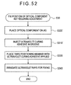
- a method for manufacturing an optical device that includes a plurality of optical components arranged on an optical path of a light beam irradiated by a light source and an optical component casing with an illumination optical axis of the light beam being set therein, in which the optical components are housed and arranged at predetermined positions on the illumination optical axis, in which at least one opening penetrating toward the inside is formed on the optical component casing, the method includes: a casing placing operation for placing the optical component casing at a predetermined position so that a part of a positioning jig is inserted to the opening; a first optical component positioning and fixing operation for housing the optical component not requiring the adjustment out of the plurality of optical components inside the optical component casing through the opening of the optical component casing, and positioning at the designed predetermined position with the use of the positioning jig inserted to the opening to fix on the optical component casing; and a second optical component positioning and fixing operation for housing the optical component requiring the adjustment out of the plurality of
- the optical component casing may be any profile as long as the plurality of optical components can be housed and arranged therein.
- the optical component casing may be a container structure or a hollow structure in the same manner as the above-described optical component casing.
- the optical component casing may be a synthetic resin molding product manufactured by molding such as injection molding in the same manner as the conventional art, a structure formed by sheet metal processing, or a structure formed by BMC.
- the optical component casing includes at least one opening penetrating toward the inside.
- the optical component casing is shifted in the casing placing operation so that the part of the positioning jig is inserted to the opening formed on the optical component casing to place the optical component casing at the predetermined position.
- the optical component not requiring the adjustment in the plurality of optical components is shifted to be housed inside the optical component casing through the opening of the optical component casing, and then the optical component not requiring the adjustment is positioned at the designed predetermined position with the use of the positioning jig inserted to the opening of the optical component casing to fix on the optical component casing.
- the optical component requiring the adjustment in the plurality of optical components is shifted to be housed inside the optical component casing through the opening of the optical component casing, and then the optical component requiring the adjustment is positioned at the designed predetermined position with the use of the positioning jig inserted to the opening of the optical component casing to fix on the optical component casing after adjusting the positions thereof.
- the optical device can easily be manufactured.
- both of the optical components not requiring the adjustment and that requiring the adjustment are positioned at the designed predetermined positions by the positioning jig, the manufacturing accuracy of the optical component casing need not to be so high as compared to an optical component casing having external position reference faces therein and being required to be highly accurately manufactured. Accordingly, the production cost of the optical component casing can be reduced, and consequently, the production cost of the optical device can be reduced.
- the optical component requiring the adjustment is positioned at the designed predetermined position, and then, the position thereof is adjusted.
- the displacement of the relative positions of the plural optical components can be prevented by adjusting the position of the optical component requiring the adjustment, thus highly accurately manufacturing the optical device.
- the position of the optical component not requiring adjustment need not to be adjusted since that is unlikely displaced, but only the position of the optical component requiring the adjustment is adjusted, thus highly accurately and promptly manufacturing the optical device.
- the first optical component positioning and fixing operation includes an optical component supporting operation for supporting the optical component not requiring the adjustment at the designed predetermined position with the use of the positioning jig, and an optical component position fixing operation for fixing the optical component not requiring the adjustment, which is supported at the designed predetermined position, on the optical component casing.
- the optical component not requiring the adjustment is supported by the positioning jig in the optical component supporting operation, the optical component not requiring the adjustment can easily be positioned at the designed predetermined position. Further, since the optical component not requiring the adjustment and being positioned on the designed predetermined position is fixed on the optical component casing in the optical component position fixing operation, the optical component not requiring the adjustment can easily be positioned and fixed on the optical component casing.
- the first optical component positioning and fixing operation further includes a positioning member abutting operation for abutting the positioning member to at least any of the optical components not requiring the adjustment, and in the optical component position fixing operation, at least any of the optical components not requiring the adjustment is fixed on the optical component casing through the positioning member.
- the positioning member abutting on at least any of the optical components not requiring the adjustment in the positioning member abutting operation, since the optical component is fixed on the optical component casing together with the positioning member in the optical component position fixing operation, the position of the optical component requiring highly accurate positioning in the optical components not requiring the adjustment, can securely be fixed by the positioning member.
- the second optical component positioning and fixing operation includes an optical component supporting operation for supporting the optical component requiring the adjustment at the designed predetermined position with the use of the positioning jig, an optical component position adjusting operation for adjusting the position of the optical component requiring the adjustment, which is supported at the designed predetermined position, and an optical component position fixing operation for fixing the adjusted optical component requiring the adjustment on the component casing.
- the optical component requiring the adjustment is supported by the positioning jig in the optical component supporting operation, the optical component requiring the adjustment can easily be positioned at the designed predetermined position. Further, even when the relative positions of the plural optical components are displaced due to manufacturing error etc. of the optical component requiring the adjustment, the relative positions of the plural optical components can be prevented from the displacement in the optical component position adjusting operation. After the position is adjusted, since the optical component requiring the adjustment is fixed on the optical component casing in the optical component position fixing operation, the highly accurate optical device can be manufactured.
- the second optical component positioning and fixing operation further includes a positioning member abutting operation for abutting the positioning member to at least any of the optical components requiring the adjustment, and in the optical component position fixing operation, at least any of the optical components requiring the adjustment is fixed on the optical component casing through the positioning member.
- the positioning member abutting on at least any of the optical components requiring the adjustment in the positioning member abutting operation, since the optical component is fixed on the optical component casing together with the positioning member in the optical component position fixing operation, the position of the optical component requiring highly accurate positioning in the optical components requiring the adjustment, can securely be fixed by the positioning member.
- the optical component position adjusting operation includes an optical image detecting process for irradiating the light beam on the plurality of optical components to detect the optical image via the plurality of optical components by an optical image detecting device, and an optical component position adjusting process for adjusting the position of the optical component requiring the adjustment by operating the positioning jig based on the optical image detected in the optical image detecting process.
- the optical image detecting device may be, for instance, that directly detects the optical image via the plurality of optical components, or that projects the optical image via the plurality of optical components on the screen in an enlarged manner to detect the optical image projected on the screen.
- the optical image detecting device can employ an image pickup element such as a CCD and a MOS sensor etc.
- the optical component position adjusting operation includes the optical image detecting process, it can be determined whether or not the plurality of optical components are positioned at the designed predetermined positions according to the optical image detected in the optical image detecting process. Further, since the optical component position adjusting operation includes the optical component position adjusting process, in such case that the plurality of optical components are not positioned at the designed predetermined positions, the positions of the optical components requiring the adjustment can be adjusted by operating the positioning jig based on the optical image detected in the optical image detecting process. Thus, the plurality of optical components are further highly accurately positioned.
- the positioning jig is controllably driven by a jig driver for driving the positioning jig, and by a controlling unit for controlling the jig driver
- the optical component position adjusting process includes an image capturing step for capturing the optical image detected in the optical image detecting process by the controlling unit to convert into an image signal, a luminance acquiring step for acquiring a luminance value by the controlling unit from the image signal converted in the image capturing step, a position adjustment amount computing step for computing a position adjustment amount of the optical component requiring the adjustment by the controlling unit based on the luminance value acquired in the luminance acquiring step, and a position adjusting step for adjusting the position of the optical component requiring the adjustment by driving the positioning jig under the control of the controlling unit based on the position adjustment amount computed in the position adjustment amount computing step.
- the controlling unit may be, for instance, a PC that includes a CPU reading and executing a control program, a video capture board inputting a signal output from the optical image detecting device to convert into an image signal, and the like. Further, each step in the optical component position adjusting process can be configured as a program to be executed by the controlling unit.
- the optical component position adjusting process includes the image capturing step, the luminance acquiring step, the position adjustment amount computing step and the position adjusting step so that the position of the optical component requiring the adjustment is adjusted with the drive control of the positioning jig by the controlling unit. Accordingly, the optical component requiring the adjustment can further accurately be positioned as compared to the case that the position of the optical component requiring the adjustment is adjusted by manually operating the positioning jigs with the optical image detected by the optical image detecting device being checked with eyes.
- the optical component position adjusting process includes an illumination area shifting step for shifting the optical component requiring the adjustment by driving the positioning jig under the control of the controlling unit and shifting the illumination area of the optical image via the plurality of optical components, and a boundary point acquiring step for acquiring a boundary point of the illumination area shifted in the illumination area shifting step by the controlling unit based on the luminance value acquired in the luminance acquiring step, and in the position adjustment amount computing step, the position adjustment amount of the optical component requiring the adjustment is computed by the controlling unit based on the boundary point of the illumination area acquired in the boundary point acquiring step.
- the optical component position adjusting process includes the illumination area shifting step and the boundary point acquiring step in addition to the image capturing step, the luminance acquiring step, the position adjustment amount computing step and the position adjusting step. Then, in the position adjustment amount computing step, the controlling unit computes the position adjustment amount of the optical component requiring the adjustment based on the boundary point of the illumination are acquired in the boundary point acquiring step. With this step, the displacement of the relative positions of the plural optical components can easily be recognized by the acquisition of the boundary position of the illumination area, thus enabling highly accurate positioning of the optical components requiring the adjustment.
- the optical component casing includes a support portion abutting on the optical component, an adhesive is filled between the optical component and the support portion, and in the optical component position fixing operation, the adhesive is cured to fix the optical component on the optical component casing.
- the adhesive can be applied thereto in advance in the optical component supporting operation or the optical component position adjusting operation, or can be applied thereto after the optical component supporting operation or the optical component position adjusting operation are completed.
- the support portion can use the lateral side of the optical component casing, or can be a component independent from the lateral side constituting the optical component casing.
- the position of the optical component since the position of the optical component is fixed on the optical component casing by the adhesive applied between the optical component and the support portion being cured, the position of the optical component can easily and promptly be fixed after positioning.
- a groove is formed on an abutting face of the support portion, which abuts on the optical component, and in the optical component position fixing operation, an adhesive is injected to the groove to fill the adhesive between the optical component and the support portion, and the adhesive is cured to fix the optical component on the optical component casing.
- the groove may penetrate through the support portion from the first end to the opposing second end.
- the groove may be formed from the first end of the support portion to the part around the opposing second end thereof, in other words, the groove may be formed so as not to penetrate through the support portion from the first end to the opposing second end.
- the adhesive is injected to the groove to fill the adhesive between the optical component and the support portion.
- the adhesive is then cured, so that the position of the optical component is fixed on the optical component casing. Accordingly, the adhesive can easily be applied (injected) between the optical component and the support portion, thus further easily and promptly fixing the position of the optical component after positioning.
- the optical component in the optical component position fixing operation, the optical component can be prevented from the adhesive unnecessarily adhering.
- the position of the optical component can easily be fixed on the optical component casing.
- a method for manufacturing an optical device that includes a plurality of optical components arranged on an optical path of a light beam irradiated by a light source and an optical component casing with an illumination optical axis of the light beam being set therein, in which the optical components are housed and arranged at predetermined positions on the illumination optical axis, in which at least one opening penetrating toward the inside is formed on the optical component casing, the method includes: an optical component positioning operation for positioning the plurality of optical components at the designed predetermined positions with the use of the positioning jig; an optical component position adjusting operation for adjusting the position of the optical component requiring the adjustment out of the plurality of optical components; a casing placing operation, after the optical component position adjusting operation, for placing the optical component casing on a predetermined position corresponding to the plurality of optical components so that the plurality of optical components are housed therein through the opening; and an optical component position fixing operation for fixing the positions of the plurality of optical components on the optical component casing
- the optical component casing may be any profile as long as the plurality of optical components can be housed and arranged therein.
- the optical component casing may be a container structure or a hollow structure in the same manner as the above-described optical component casing.
- the casing body may be a synthetic resin molding product manufactured by molding such as injection molding in the same manner as the conventional art, a structure formed by sheet metal processing, or a structure formed by BMC.
- the plurality of optical components are positioned at the designed predetermined positions by the positioning jig in the optical component positioning operation. Further, in the optical component position adjusting operation, the position of the optical component requiring the adjustment in the plurality of positioned optical components is adjusted. Further, in the casing placing operation, the optical component casing is shifted so that the plurality of optical components are inserted to the inside through the opening of the optical component casing to place the optical component casing at the predetermined position corresponding to the plurality of optical components. Thereafter, the positions of the plurality of optical components are fixed on the optical component casing in the optical component position fixing operation. Thus, the optical device can easily be manufactured.
- the manufacturing accuracy of the optical component casing need not to be so high as compared to an optical component casing being required to be highly accurately manufactured.
- the optical component casing only requires to have at least one opening. Accordingly, the production cost of the optical component casing can further be reduced, and consequently, the production cost of the optical device can further be reduced.
- the optical component position adjusting operation is performed after the optical component positioning operation, even when the relative positions of the plural optical components are displaced due to manufacturing error etc. of the plural optical components at the placement of the plural optical components on the designed predetermined positions with the use of the positioning jig, the relative positions of the plural optical components can be prevented from the displacement by adjusting the positions of the optical components requiring the adjustment, thus highly accurately manufacturing the optical device.
- the position of the optical component not requiring the adjustment need not to be adjusted since that is unlikely displaced, but only the position of the optical component requiring the adjustment is adjusted, thus highly accurately and promptly manufacturing the optical device.
- the optical device further includes: a positioning member abutting operation for abutting the positioning member to a group of the plurality of optical components, in which, in the optical component position fixing operation, the group of optical components are fixed on the optical component casing through the positioning members.
- the positioning member abutting on the group of optical components out of the plurality of optical components in the positioning member abutting operation, since the optical component is fixed on the optical component casing together with the positioning member in the optical component position fixing operation, the position of the group of optical components requiring highly accurate positioning in the plurality of optical components, can securely be fixed by the positioning member.
- the optical component position adjusting operation includes an optical image detecting process for irradiating the light beam on the plurality of optical components to detect the optical image via the plurality of optical components by an optical image detecting device, and an optical component position adjusting process for adjusting the position of the optical component requiring the adjustment by operating the positioning jig based on the optical image detected in the optical image detecting process.
- the optical image detecting device may be, for instance, that directly detects the optical image via the plurality of optical components, or that projects the optical image via the plurality of optical components on the screen in an enlarged manner to detect the optical image projected on the screen.
- the optical image detecting device can employ an image pickup element such as a CCD and a MOS sensor etc.
- the optical component position adjusting operation includes the optical image detecting process, it can be determined whether or not the plurality of optical components are positioned at the designed predetermined positions according to the optical image detected in the optical image detecting process. Further, since the optical component position adjusting operation includes the optical component position adjusting process, in such case that the plurality of optical components are not positioned at the designed predetermined positions, the positions of the optical components requiring the adjustment can be adjusted by operating the positioning jig based on the optical image detected in the optical image detecting process. Thus, the plurality of optical components are further highly accurately positioned.
- the positioning jig is controllably driven by a jig driver for driving the positioning jig, and by a controlling unit for controlling the jig driver
- the optical component position adjusting process includes an image capturing step for capturing the optical image detected in the optical image detecting process by the controlling unit to convert into an image signal, a luminance acquiring step for acquiring a luminance value by the controlling unit from the image signal converted in the image capturing step, a position adjustment amount computing step for computing a position adjustment amount of the optical component requiring the adjustment by the controlling unit based on the luminance value acquired in the luminance acquiring step, and a position adjusting step for adjusting the position of the optical component requiring the adjustment by driving the positioning jig under the control of the controlling unit based on the position adjustment amount computed in the position adjustment amount computing step.
- the controlling unit may be, for instance, a PC that includes a CPU reading and executing a control program, a video capture board inputting a signal output from the optical image detecting device to convert into an image signal, and the like. Further, each step in the optical component position adjusting process can be configured as a program to be executed by the controlling unit.
- the optical component position adjusting process includes the image capturing step, the luminance acquiring step, the position adjustment amount computing step and the position adjusting step so that the position of the optical component requiring the adjustment is adjusted with the drive control of the positioning jig by the controlling unit. Accordingly, the optical component requiring the adjustment can further accurately be positioned as compared to the case that the position of the optical component requiring the adjustment are adjusted by manually operating the positioning jig with the optical image detected by the optical image detecting device being checked with eyes.
- the optical component position adjusting process includes an illumination area shifting step for shifting the optical component requiring the adjustment by driving the positioning jig under the control of the controlling unit and shifting the illumination area of the optical image via the plurality of optical components, and a boundary point acquiring step for acquiring a boundary point of the illumination area shifted in the illumination area shifting step by the controlling unit based on the luminance value acquired in the luminance acquiring step, and the position adjustment amount computing step computes the position adjustment amount of the optical component requiring the adjustment by the controlling unit based on the boundary point of the illumination area acquired in the boundary point acquiring step.
- the optical component position adjusting process includes the illumination area shifting step and the boundary point acquiring step in addition to the image capturing step, the luminance acquiring step, the position adjustment amount computing step and the position adjusting step. Then, in the position adjustment amount computing step, the controlling unit computes the position adjustment amount of the optical component requiring the adjustment based on the boundary point of the illumination are acquired in the boundary point acquiring step. With this step, the displacement of the relative positions of the plural optical components can easily be recognized by the acquisition of the boundary position of the illumination area, thus positioning of the optical component requiring the adjustment highly accurately.
- the optical component casing includes a support portion abutting on the optical component, an adhesive is filled between the optical component and the support portion, and in the optical component position fixing operation, the adhesive is cured to fix the optical component on the optical component casing.
- the adhesive can be applied thereto in advance in the optical component position adjusting operation, or can be applied thereto after the optical component position adjusting operation or the casing placing operation are completed.
- the support portion can use the lateral side of the optical component casing, or can be a component independent from the lateral side constituting the optical component casing. According to this arrangement, in the optical component position fixing operation, since the position of the optical component is fixed on the optical component casing by curing the adhesive applied between the optical component and the support portion, the position of the optical component can easily and promptly be fixed after positioning.
- a groove is formed on an abutting face of the support portion, which abuts on the optical component, and in the optical component position fixing operation, an adhesive is injected to the groove to fill the adhesive between the optical component and the support portion, and the adhesive is cured to fix the optical component on the optical component casing.
- the groove may penetrate through the support portion from the first end to the opposing second end.
- the groove may be formed from the first end of the support portion to the part around the opposing second end thereof, in other words, the groove may be formed so as not to penetrate through the support portion from the first end to the opposing second end.
- the adhesive is injected to the groove to fill the adhesive between the optical component and the support portion.
- the adhesive is then cured, so that the position of the optical component is fixed on the optical component casing. Accordingly, the adhesive can easily be applied (injected) between the optical component and the support portion, thus easily and promptly fixing the position of the optical component after positioning.
- the optical components can be prevented from the adhesive unnecessarily adhering.
- the position of the optical component can easily be fixed on the optical component casing.
- Fig. 1 is a perspective view showing an example of a projector including an optical unit manufactured by a manufacturing method of an optical unit according to the present embodiment.
- the projector 1 modulates a light beam irradiated by a light source in accordance with image information and projects the light beam on a projection surface such as a screen in an enlarged manner.
- the projector 1, as shown in Fig. 1, has a planarly-viewed L-shaped optical unit 2 and a projection lens 3 as a projection optical device connected to an end of the optical unit 2.
- the projector 1 includes a power source unit for providing electric power supplied from the outside to the components of the projector 1, a control board for controllably driving a below-described liquid crystal panel of the optical unit 2 and a cooling unit having a cooling fan for blowing cooling air to the components of the projector 1 in addition to the optical unit 2 and the projection lens 3.
- the respective components of the projector 1 such as the optical unit 2, a part of the projection lens 3, the power source unit, the control board and the cooling unit etc. are housed in an exterior case 20.
- the projection lens 3 is arranged in the state that an image can be projected outside through an opening of the exterior case 20.
- the optical unit 2 forms an optical image in accordance with image information provided from the outside.
- the optical unit 2 includes an optical component casing 25 that has a casing body constituted of a container 25A formed in a container-shape and a lid 25B for closing an opening of the container 25, a plurality of optical components arranged and housed in the optical component casing 25 and a head 26 connected to the optical component casing 25 to support the projection lens 3 and an electric optical device 24.
- the projection lens 3 enlarges and projects the optical image modulated by the optical unit 2 in accordance with image information.
- the projection lens 3 is a lens set including a plurality of lenses housed in a cylindrical lens barrel, which has a lever (not shown) capable of changing the relative position of the plurality of lenses so that the focus and magnification of the projected image can be adjusted.
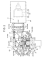
- Fig. 2 is a plan view schematically showing the inside structure of the optical unit 2. Specifically, Fig. 2 is an illustration of the optical unit 2 with the lid 25B removed.
- the optical components of the projector 1 include an integrator illuminating optical system 21, a color-separating optical system 22, a relay optical system 23 and the electric optical device 24 integrating an optical modulator and a color-combining optical device.
- the integrator illuminating optical system 21 is an optical system for equalizing the illuminance of the light beam irradiated by the light source on a plane orthogonal to the illumination optical axis. As shown in Fig. 2, the integrator illuminating optical system 21 has a light source device 211, a first lens array 212, a second lens array 213, a polarization converter 214 and a superposing lens 215.
- the light source device 211 has a light source lamp 216 (a radial light source), a reflector 217 and a protection glass 218 covering the light-irradiation side of the reflector 217.
- the radial light beam irradiated by the light source lamp 216 is reflected by the reflector 217 to be an approximately parallel light beam and is irradiated toward the outside.
- a high-pressure mercury lamp is used as the light source lamp 216 and a parabolic mirror is used as the reflector 217.
- the light source lamp 216 may not be a high-pressure mercury lamp but may be a metal halide lamp or a halogen lamp.
- a parabolic mirror is used as the reflector 217, a parallelizing concave lens disposed on an irradiation-side of a reflector of an ellipsoidal mirror may alternatively be used.
- the first lens array 212 has small lenses arranged in a matrix, the lenses having substantially rectangular profile seen in the illumination optical axis direction.
- the respective lenses separates the light beam irradiated by the light source lamp 216 into sub-beams and emits the sub-beams in the illumination optical axis direction.
- the second lens array 213 is arranged approximately in the same manner as the first lens array 212, which includes small lenses arranged in a matrix.
- the second lens array 213 together with the superposing lens 215 superposes the image of the respective small lenses of the first lens array 212 onto the image formation areas of the below-described liquid crystal panels 241R, 241G and 241B of the electric optical device 24.
- the polarization converter 214 converts the light from the second lens array 213 into substantially uniform polarized light, thereby enhancing the light utilization efficiency of the electric optical device 24.
- the respective sub-beams converted into substantially uniform polarized light by the polarization converter 214 are substantially superposed on the image formation areas of the below-described liquid crystal panels 241R, 241G and 241B of the electric optical device 24 by the superposing lens 215. Since only one-type of polarized light can be used in a projector using the liquid crystal panels 241R, 241G and 241B that modulate a polarized light, approximately half of the light beam from the light source lamp 216 emitting random polarized light cannot be used. Accordingly, with the use of the polarization converter 214, the light beam irradiated by the light source lamp 216 is converted into substantially uniform polarized light to enhance the light utilization efficiency of the electric optical device 24. Incidentally, such polarization converter 214 is disclosed in, for instance, JP H08-304739A.
- the color-separating optical system 22 has two dichroic mirrors 221 and 222, and a reflection mirror 223.
- the plurality of sub-beams irradiated by the integrator illuminating optical system 21 are separated into three color lights of red (R), green (G) and blue (B) by the two dichroic mirrors 221.
- the relay optical system 23 has an incident-side lens 231, a relay lens 233, and reflection mirrors 232 and 234.
- the relay optical system 23 guides the color light (blue light) separated by the color-separating optical system 22 toward the below-described liquid crystal panel 241B of the electric optical device 24.
- the dichroic mirror 221 of the color-separating optical system 22 transmits the green light component and blue light component of the light beam irradiated by the integrator illuminating optical system 21 and reflects the red light component.
- the red light reflected by the dichroic mirror 221 is reflected by the reflection mirror 223, which reaches to the liquid crystal panel 241R for red color through the field lens 224.
- the field lens 224 converts the respective sub-beams irradiated by the second lens array 213 into a light beam parallel to the central axis (main beam) thereof.
- the field lenses 224 provided on the light-incident side of the other liquid crystal panels 241G and 241B function in the same manner.
- the green light is reflected by the dichroic mirror 222, which reaches to the liquid crystal panel 241G for green light through the field lens 224.
- the blue light passes through the dichroic mirror 222, which passes through the relay optical system 23 to reach the liquid crystal panel 241B for blue light through the field lens 224.
- the relay optical system 23 is used for the blue light in order to avoid deterioration in the light utilization efficiency on account of light dispersion and the like caused by the longer length of the optical path of the blue light than the optical path of the other color light.
- the relay optical system 23 is used for directly transmitting the sub-beams incident on the incident-side lens 231 to the field lens 224.
- the blue light of the three color lights passes through the relay optical system 23, the red light, for instance, may alternatively pass through the relay optical system 23.
- the electric optical device 24 modulates the incident light beam in accordance with image information to form a color image.
- the electric optical device 24 has three incident-side polarization plates 242 on which the respective color lights separated by the color-separating optical system 22 are incident, the liquid crystal panels 241R, 241G and 241B (optical modulators) and irradiate-side polarization plates 243 disposed on the downstream of the respective incident-side polarization plates 242, and a cross dichroic prism 244 (color-combining optical device).
- the liquid crystal panels 241R, 241G and 241B use, for instance, a polycrystalline silicon TFT as a switching element, which has a pair of opposing transparent substrates with liquid crystal sealed therebetween.
- the liquid crystal panels 241R, 241G and 241B irradiate the light beam incident thereon through the incident-side polarization plates 242 after modulating in accordance with image information.
- the liquid crystal panels 241R, 241G and 241B are held and accommodated in a holder frame (not shown).
- the incident-side polarization plate 242 transmits a polarized light in a predetermined direction out of the respective color lights separated by the color-separating optical system 22 and absorbs the other light beam, which have a substrate made of sapphire glass and the like with a polarization film attached thereon.
- the irradiation-side polarization plate 243 is also arranged substantially in the same manner as the incident-side polarization plate 242, which transmits the polarized light in a predetermined direction out of the light beam irradiated by the liquid crystal panels 241R, 241G and 241B, where the polarization axis of the transmitted polarized light is set orthogonal to the polarization axis of the polarized light passed through the incident-side polarization plate 242.
- the cross dichroic prism 244 combines the optical image irradiated by the irradiation-side polarization plate 243 and modulated for each color light to form a color image.
- a dielectric multi-layer film for reflecting the red light and a dielectric multi-layer film for reflecting the blue light are formed along the boundaries of four right-angle prisms approximately in X-shape, the dielectric multi-layer films combining the three color lights.
- the cross dichroic prism 144 is fixed on a mount (not shown). Further, the liquid crystal panels 241R, 241G and 241B, and the three irradiation-side polarization plates 243 are respectively fixed on the three light incident sides of the cross dichroic prism 244 to be unitized.
- the unit, in which the cross dichroic prism 244, the mount, the liquid crystal panels 241R, 241G and 241B and the three irradiation-side polarization plates 243 are integrated, is called as a "prism unit" for convenience.
- the electric optical device 24 may be equipped with a visual-angle corrector plate arranged between the incident-side polarization plate 242 and the irradiation-side polarization plate 243 to correct the visual field angle of the optical image formed by the liquid crystal panels 241R, 241G and 241B in addition to the liquid crystal panels 241R, 241G and 241B, the incident-side polarization plate 242, the irradiation-side polarization plate 243 and the cross dichroic prism 244.
- the visual field angle of the projection image is enlarged and the contrast of the projected image is enhanced since the visual-angle corrector plate is arranged.
- the optical component casing 25 includes the container 25A in which the various optical components of the above-described optical systems 21, 22 and 23 and the electric optical device 24 are housed, the lid 25B (Fig. 1) for closing the upper opening of the container 25A, a positioning member 253 for positioning the optical components of the optical systems 21, 22 and 23 excluding the light source device 211 at predetermined positions in the container 25A, and rework members 254X, 254Y and 254Z (not shown here) appropriately mounted on the outer side of the optical component casing 25 to be able to rework the various optical components housed and arranged in the container 25A.
- Fig. 3 is a perspective view showing structure of the container 25A.
- the container 25A made of an aluminum plate by sheet metal processing includes a light source housing 250 for housing the light source device 211, and a component housing 251 for housing the optical components of the optical systems 21, 22 and 23 (Fig. 2) excluding the light source device 211.
- the light source housing 250 and the component housing 251 are formed in a container-shape by drawing with the lower side of the light source housing 250 being opened and the upper side of the component housing 251 being opened.
- An opening 251H (Fig. 3) is formed on a connection of the light source housing 250 with the component housing 251 by cutting etc. so that the light beam irradiated by the light source device 211 passes through the opening 251H.
- the light source housing 250 and the component housing 251 may be formed with a single plate by drawing. Further, the light source housing 250 and the component housing 251 may be respectively formed with two plates by drawing so that the two housings are mechanically joined by a screw etc. or by welding.
- the light source housing 250 houses and arranges the light source device 211 (Fig. 2) from the opening (not shown) on the lower side. Though not shown, a slit-shaped opening is formed on a lateral side of the light source housing 250 by cutting etc. so that the air heated by the heat generated at the light source device 211 does not stay inside the light source housing 250.
- an end of the component housing 251 is connected to the light source housing 250, and the other end thereof is formed in an approximately planarly-viewed C-shaped container to which the head 26 is connected.
- a plurality of holes 251A are formed on the lateral side by cutting and folding parts of the lateral side to the inside of the component housing 251 corresponding to the positions of the optical components 212 to 215, 231 and 233 (Fig. 2). Further, a plurality of circular holes 251C are formed on the lateral side to penetrate toward the inside corresponding to the positions of the optical components 223, 232 and 234 (Fig. 2). Cutouts 251J are formed on an inner lateral side of the approximately planarly-viewed C-shape by cutting etc. so that the three color lights irradiated by the light source device 211 (Fig. 2) and separated by the color-separating optical system 22 (Fig. 2) can pass through the cutouts 251J toward the electric optical device 24 (Fig. 2).
- a plurality of burring holes with screw grooves are formed on a bottom side and an upper end of the component housing 251.
- the lid 25B is an aluminum plate, which is formed by cutting etc. to close an upper opening of the component housing 251 of the container 25A. Though not shown, a plurality of holes are formed on the lid 25B so that the lid 25B is fixed to the container 25A by screws etc. through the holes and burring holes (not shown) formed on the container 25A.
- the inner sides of the light source housing 250 and the component housing 251 of the above-described container 25A and the lower side of the lid 25B are coated with anodized black-aluminum.
- the positioning member 253 include first positioning members 253A as orthogonal arrangement positioning members for respectively positioning the first lens array 212, the second lens array 213, the polarization converter 214, the superposing lens 215, the incident-side lens 231 and the relay lens 233, second positioning members 253B (Fig. 2) as inclined arrangement positioning members for respectively positioning the dichroic mirrors 221 and 222, and third positioning members 253C as parallel arrangement positioning members for respectively positioning the reflection mirrors 223, 232 and 234.
- the positioning member 253 will be described at the same time when holding structure of the optical component is described.
- the rework members 254X, 254Y and 254Z will be described in detail after the holding structure of the optical component is described.
- the head 26 is made of magnesium alloy, which is formed in an approximately L shape-sided portion. As shown in Fig. 2, the head 26 integrates the projection lens 3 and a plurality of optical elements.
- the head 26 includes a lens supporter 261 formed on an outer vertical side of the approximately L shape-sided portion, a mount face 262 formed on an upper horizontal side of the approximately L shape-sided portion, and field lens holders 263 projected on the mount face 262.
- the head 26 may be made of aluminum, magnesium and titanium or alloy containing the above metal as main components without limiting to the magnesium alloy.
- the lens supporter 261 is formed in a rectangular shape, on which fixing female screw holes (not shown) are formed on four corners of the rectangular shape by penetrating through it in order to fix the projection lens 3.
- the lens supporter 261 supports and fixes the projection lens 3 by screwing screws etc. into the fixing female screw holes via holes (not shown) of the projection lens 3.
- the mount face 262 is formed in an approximately planarly-viewed rectangular shape.
- the prism unit is mounted and fixed on the mount face 262 at the approximate center in a horizontal direction near the lens supporter 261.
- the prism unit is fixed on the mount face 262 through the mount.
- Three cutouts 262A for circulating the cooling air blown from the cooling unit are formed on the mount face 262 at the side of the liquid crystal panels 241R, 241G and 241B.
- the field lens holders 263 extends upward from corners of the cutouts 262A formed on the mount face 262 to support and fix the field lens 224.
- a plurality of holes are formed on the mount face 262 of the above-described head 26 so that the head 26 is fixed on the container 25A by screws etc. through the holes and the burring holes (not shown) formed on the container 25A.
- fixing structure of the incident-side polarization plate 242 may employ a configuration that a polarization film is attached to the light-irradiation side of the field lens 224 or structure that holds and fixes the incident-side polarization plate 242 on a member projected upward from the mount face 262 in the same manner as the field lens holder 263.
- the holding structures of the optical components can be classified into three holding structures by grouping similar structures.
- the holding structures can be classified into a lens holding structure for holding the first lens array 212, the second lens array 213, the polarization converter 214, the superposing lens 215, the incident-side lens 231 and the relay lens 233, a dichroic mirror holding structure for holding the dichroic mirrors 221 and 222, and a reflection mirror holding structure for holding the reflection mirrors 223, 232 and 234.
- the above three holding structures will be sequentially described.
- Fig. 4 is an illustration to explain the lens holding structure. As mentioned above, since the holding structures of the optical components 212 to 215, 231 and 233 have similar structures, the holding structure of the superposing lens 215 will mainly be described here.
- the planarly-viewed circular superposing lens 215 is a convex lens, of which a light-incident side and a light-irradiation side are spherically bulged.
- Two first positioning members 253A out of the above-described plurality of first positioning members 253A are used as members for holding the superposing lens 215.
- the first positioning member 253A is made of synthetic resin (acrylic material) transmitting ultraviolet ray and formed in a quadratic prism member which is inserted through the hole 251A formed on the lateral side of the container 25A.
- a groove 253A1 having an approximately V-shaped cross-section is formed on an end of the quadratic prism of the first positioning member 253A.
- the groove 253A1 is formed to have the approximately same shape as a cross-section of an outer periphery of the superposing lens 215.
- a rework screw hole 253A2 is formed on the other end of the first positioning member 253A with the rework screw hole 253A2 as a screwing configuration extending toward the end.
- the cut and folded part of the lateral side serves as a support face 251K of the first positioning member 253A.
- the first positioning members 253 sandwich the superposing lens 215 from left and right directions by the grooves 253A1 abutting on the outer periphery of the superposing lens 215 through the holes 251A formed on the lateral side of the container 25A.
- an ultraviolet curing adhesive is filled between the first positioning member 253 and the support face 251K, and between the groove 253A1 of the first positioning member 253 and the outer periphery of the superposing lens 215, so that the superposing lens 215 is held and fixed on the optical component casing 25 by curing the adhesive.
- Fig. 5 is an illustration to explain the dichroic mirror holding structure. As mentioned above, since the holding structures of the dichroic mirrors 221 and 222 have similar structures, the holding structure of the dichroic mirror 222 will mainly be described here.
- the dichroic mirror 222 is an approximately planarly-viewed rectangular shape, which is held by the second positioning member 253B.
- the second positioning member 253B includes a plate-shaped mount 253B1 fixed on a bottom side of the component housing 251 of the container 25A, a pair of plate members 253B2 fixed on an upper side of the mount 253B1 and having an L-shaped cross-section, and spacers 253B3 interposed between the pair of plate members 253B2 and left and right ends of the dichroic mirror 222.
- the pair of plate members 253B2 opposes to the lateral side of the component housing 251 of the container 25A in approximately parallel, with an end of the L-shaped cross-sectional shape being fixed on the upper side of the mount 253B1 and the other end thereof extending upward the mount 253B1.
- the dichroic mirror 222 is arranged between the pair of plate members 253B2 in an inclined manner so that left and right ends of the dichroic mirror 222 opposes to the other ends of the plate members 253B2.
- a part of the other end is cut and folded toward the opposing plate member 253B2 in a triangular shape, which defines a support face 253B4 for supporting the spacer 253B3.
- An opening 253B5 is formed on the other end near the field lens 224 (Fig. 2) out of the other ends of the pair of plate members 253B2 so that the green light reflected by the dichroic mirror 222 is passed through the opening 253B5.
- the spacer 253B3 is a triangular prism member made of synthetic resin (acrylic material) transmitting ultraviolet ray in the same manner as the first positioning member 253A.
- a rework screw hole 253B6 (not shown) is formed on an upper end of the spacer 253B3 with the rework screw hole 253B6 extending toward a lower end thereof.
- the spacer 253B3 is supported by the support face 253B4 and interposed between the left and right ends of the dichroic mirror 222 and the plate members 253B2.
- an inclined direction of a slanted face of the triangular prism of the spacer 253B3 is configured to be the approximately same direction as an inclined direction of the dichroic mirror 222.
- the ultraviolet curing adhesive is filled between the spacer 253B3 and the support face 253B4, and between the slanted face of the spacer 253B3 and an outer periphery of the dichroic mirror 222, so that the dichroic mirror 222 is held and fixed on the optical component casing 25 by curing the adhesive.
- the other holding structure of the dichroic mirror 221 is similar to the above-described holding structure of the dichroic mirror 222.
- Fig. 6 is an illustration to explain the reflection mirror holding structure. As mentioned above, since the holding structures of the reflection mirrors 223, 232 and 234 have similar structures, the holding structure of the reflection mirror 232 will mainly be described here.
- the reflection mirror 232 is an approximately planarly-viewed rectangular shape, of which an end has a reflection face depositing highly reflective aluminum etc.
- the above-described third positioning member 253C is used as a member for holding the reflection mirror 232.
- the third positioning member 253C made of synthetic resin (acrylic member) transmitting ultraviolet ray includes a plate body 253C1 and cylindrical four pins 253C2 projected from four corners of an end of the plate body 253C1 with the pins 253C2 being orthogonal to the end.
- a rework screw hole 253C3 extending inside the pin 253C2 is formed on a back side of the plate body 253Cl.
- the pin 253C2 is inserted to the third positioning member 253C through a hole 251C formed on the lateral side of the container 25A so that an tip end of the pin 253C2 abuts on a back side of a reflection face of the reflection mirror 232.
- an ultraviolet curing adhesive is filled between the pin 253C2 and the back side of the reflection face of the reflection mirror 232, and between a periphery of the pin 253C2 and the hole 251C, so that the reflection mirror 232 is held and fixed on the optical component casing 25 by curing the adhesive.
- first positioning member 253A, the spacer 253B3 and the third positioning member 253C are made of acrylic material, they may be made of other synthetic resins transmitting ultraviolet ray or, alternatively, may be made of optical glass, crystal, sapphire glass, quartz or the like.
- the dichroic mirror holding structure and the reflection mirror holding structure may employ a wide variety of adhesives, preferably, the main component is acrylate and its viscosity is 17000P.
- Figs. 7 to 9 are perspective views respectively showing structures of the rework members 254X, 254Y and 254Z.
- the rework member 254X releases the adhered and fixed state on the optical component casing 25.
- the rework member 254X is formed in a shape having an approximately c-shaped cross-section by bending an aluminum plate, and includes a support member 254A of which a hole 254A1 is formed on an end opposite to an opening side, and a rework screw 254B disposed on the hole 254A1 of the support member 254A to screw into the rework screw hole 253A2 of the first positioning member 253A.
- the rework member 254Y releases the adhered and fixed state on the optical component casing 25.
- the rework member 254Y is formed in a shape having an approximately c-shaped cross-section by bending an aluminum plate, and includes a support member 254A of which a hole 254A1 is formed on an end opposite to an opening side, and a rework screw 254B disposed on the hole 254A1 of the support member 254A to screw into the rework screw hole 253B6 of the spacer 253B3.
- the rework member 254Z releases the adhered and fixed state on the optical component casing 25.
- the rework member 254Z is formed in a shape having an approximately c-shaped cross-section by bending an aluminum plate, and includes a support member 254A of which a hole 254A1 is formed on an end opposite to an opening side, and a rework screw 254B disposed on the hole 254A1 of the support member 254A to screw into the rework screw hole 253C3 of the plate body 253C1.
- Fig. 10 is a flowchart explaining the manufacturing method of the optical unit 2 according to the present embodiment. Referring to Fig. 10, a manufacturing method of the optical unit 2 will be described below.
- the light source device 211 is housed and arranged in the light source housing 250 of the container 25A.
- the projection lens 3 is placed on the lens supporter 261 of the head 26, the electric optical device 24 is mounted and fixed on the mount face 262, and the field lens 224 is held and fixed on the field lens holder 263.
- the head 26 is connected to the component housing 251 of the container 25A by a screw (not shown) etc.
- step S1 optical component housing operation.
- the holding structures of the optical components can be classified into the three holding structures of the lens holding structure, the dichroic mirror holding structure and the reflection mirror holding structure by grouping similar structures, hereinafter, a lens housing arrangement method, a dichroic mirror housing arrangement method and a reflection mirror housing arrangement method are sequentially described.
- Fig. 11 is a flowchart to explain the lens housing arrangement method.
- the housing arrangement method of the optical components 212 to 215, 231 and 233 are similar, the housing arrangement method of the superposing lens 215 will mainly be described here with reference to Figs. 4 and 11. Note that, similar housing arrangement methods are applied to other optical components 212 to 214, 231 and 233.
- step S111 an ultraviolet curing adhesive is applied on the grooves 253A1 and the peripheries of the two first positioning members 253A.
- the first positioning members 253 with the adhesive applied are inserted into the holes 251A formed on the lateral side of the container 25A to place the superposing lens 215 so as to be sandwiched between both left and right sides thereof (step S112: positioning member inserting process). At this time, the first positioning member 253 is held by the support face 251K.
- the superposing lens 215 is housed in the component housing 251 from the upper side of the component housing 251 so as to be arranged between the two first positioning members 253 placed in the step S112 (step S113: optical component housing process), and the outer periphery of the superposing lens 215 abuts on the grooves 253A1 of the first positioning members 253 (step S114: positioning member abutting process).
- Fig. 12 is a flowchart explaining the dichroic mirror housing arrangement method.
- the housing arrangement method of the dichroic mirror 222 will mainly be described here with reference to Figs. 5 and 12. Note that, a similar housing arrangement method is applied to the dichroic mirror 221.
- the ultraviolet curing adhesive is applied on the peripheries of the two spacers 253B3 (step S121).
- step S122 spacer placing process
- the dichroic mirror 222 is arranged between the pair of plate members 253B2 in an inclined manner against the end side of the plate members 253B2 (step S123: optical component arranging process) to abut on the spacers 253B3 mounted on the support faces 253B4 in the step S122 (step S124: spacer abutting process).
- the second positioning member 253B in which the dichroic mirror 222 is held is housed in the component housing 251 of the container 25A to fix the mount 253B1 on the bottom side of the component housing 251 (step S125).
- Fig. 13 is a flowchart explaining the reflection mirror housing arrangement method.
- the housing arrangement method of the reflection mirror 232 will mainly be described here with reference to Figs. 6 and 13. Note that, similar housing arrangement methods are applied to other reflection mirrors 223 and 234.
- the ultraviolet curing adhesive is applied on tip ends and the peripheries of the four pins 253C2 of the third positioning member 253C (step S131).
- step S132 positioning member abutting process
- the reflection mirror 232 is housed in the component housing 251 from the upper side of the component housing 251 to oppose the pins 253C2 of the third positioning member 253C placed in the step S132 (step S133: optical component housing process), and the back side of the reflection face of the reflection mirror 232 abuts on the tip ends of the pins 253C2 of the third positioning member 253C (step S134: positioning member abutting process).
- step S2 optical component positioning operation
- the light source device 211 is operated to irradiate the light beam of white light, an image light, which is the irradiated light beam after passing through the various optical components, is projected on a screen (not shown) through the projection lens 3, the positions of the various optical components are adjusted while the projected image is checked, and the optical components are positioned at the predetermined positions.
- the various optical components are positioned at the predetermined positions on the illumination optical axis of the light beam irradiated by the light source device 211 to eliminate the shade in the projected image.
- an optical axis adjustment fixture (not shown) is engaged with the optical components 212 to 215, 231 and 233 from the outside of the optical component casing 25. While the projected image is checked, the optical axis adjustment fixture is operated so that the positions of the optical components 212 to 215, 231 and 233 are adjusted according to five axes respectively in a horizontal direction, a vertical direction, a cross direction, an out-plane rotary direction around the horizontal direction as its axis, and an out-plane rotary direction around the vertical direction as its axis of the optical components.
- the first positioning members 253A follow when the optical components 212 to 215, 231 and 233 shift, so that the first positioning members 253A position the optical components 212 to 215, 231 and 233 at the predetermined positions.
- an optical axis adjustment fixture (not shown) is also engaged with the dichroic mirrors 221 and 222. While the projected image is checked, the optical axis adjustment fixture is operated so that the positions of the dichroic mirrors 221 and 222 are adjusted according to five axes respectively in a horizontal direction, a vertical direction, a cross direction, an out-plane rotary direction around the horizontal direction as its axis, and an out-plane rotary direction around the vertical direction as its axis of the dichroic mirrors.
- the spacers 253B3 follow when the dichroic mirrors 221 and 222 shift, so that the spacers 253B3 position the dichroic mirrors 221 and 222 at the predetermined positions.
- an optical axis adjustment fixture (not shown) is also engaged with the plate bodies 253C1 of the third positioning members 253C. While the projected image is checked, the optical axis adjustment fixture is operated to shift the plate bodies 253C1.
- the reflection mirrors 223, 232 and 234 follow when the plate bodies 253C1 shift, so that the positions of the reflection mirrors 223, 232 and 234 are adjusted according to five axes respectively in a horizontal direction, a vertical direction, a cross direction, an out-plane rotary direction around the horizontal direction as its axis, and an out-plane rotary direction around the vertical direction as its axis of the reflection mirrors.
- the third positioning members 253C hold the reflection mirrors 223, 232 and 234 at the predetermined positions so that the third positioning members 253C position the reflection mirrors 223, 232 and 234 at the predetermined positions.
- step S2 after positioning the various optical components 212 to 215, 221 to 223 and 231 to 234, the positions of the various optical components are fixed on the optical component casing 25 by irradiating ultraviolet ray among the members to cure the ultraviolet curing adhesive (step S3: optical component position fixing operation).
- ultraviolet ray is irradiated from the lateral side of the container 25A toward the first positioning members 253A.
- the irradiated ultraviolet ray passes through the first positioning members 253A to cure the ultraviolet curing adhesive applied between the first positioning members 253A and the support faces 251K as well as the ultraviolet curing adhesive applied between the grooves 253A1 of the first positioning members 253A and the peripheral ends of the optical components 212 to 215, 231 and 233.
- ultraviolet ray is irradiated from the upper side of the container 25A toward the spacers 253B3.
- the irradiated ultraviolet ray passes through the spacers 253B3 to cure the ultraviolet curing adhesive applied between the spacers 253B3 and the support faces 253B4.
- the irradiated ultraviolet ray also cures the ultraviolet curing adhesive applied between the peripheries of the spacers 253B3 and the plate members 253B2 as well as the ultraviolet curing adhesive applied between the spacers 253B3 and the left and right ends of the dichroic mirrors 221 and 222.
- ultraviolet ray is irradiated from the lateral side of the container 25A toward the third positioning members 253C.
- the irradiated ultraviolet ray passes through the plate body 253C1 and the pins 253C2 to cure the ultraviolet curing adhesive applied between the peripheries of the pins 253C2 and the holes 251C as well as the ultraviolet curing adhesive applied between the tip ends of the pins 253C2 and the back sides of the reflection faces of the reflection mirrors 223, 232 and 234.
- step S4 the lid 25B is connected to the container 25A by a screw etc. (step S4) to manufacture the optical unit 2.
- a hole for engaging the optical axis adjustment fixture (not shown) with the optical components housed inside and a hole for irradiating ultraviolet ray toward the spacers 253B3 may be formed on the lid 25B so that the lid 25B is connected to the container 25A after the step S1, and the steps S2 and S3 are performed in the above state.
- step S6 in the optical unit 2 manufactured according to the operation of the above-described steps S1 to S4, when the optical component requires to be replaced etc. and the optical component is removed from the optical component casing 25 (step S5), a rework operation (step S6) is performed.
- step S6 since the above-described rework members 254X, 254Y and 254Z are used, refer to Figs. 7 to 9 appropriately when the rework operation (step S6) is described.
- the opening side of the support member 254A of the rework member 254X abuts on a position corresponding to the hole 251A on the lateral side of the container 25A.
- the rework screw 254B arranged on the hole 254A1 of the support member 254A is screwed to the rework screw hole 253A2 formed on the first positioning member 253A.
- the rework screw 254B is then rotated in a direction screwing into the rework screw hole 253A2 to change the screwing state.
- the adhered state between the first positioning member 253A and the support face 251K is released, as is the adhered state between the groove 253A1 of the first positioning member 253A and the outer periphery of the superposing lens 215, so that the superposing lens 215 is removed from the optical component casing 25.
- the reflection mirrors 223, 232 and 234 When the reflection mirrors 223, 232 and 234 are removed, the following will be performed. As mentioned above, since the holding structures of the reflection mirrors 223, 232 and 234 have similar structures, the rework method of the reflection mirror 232 will mainly be described here.
- the opening side of the support member 254A of the rework member 254Z abuts on the lateral side of the container 25A so that the third positioning member 253C is positioned inside the c-shaped support member 254A.
- the rework screw 254B arranged on the hole 254A1 of the support member 254A is screwed to the rework screw hole 253C3 formed on the plate body 253C1 of the third positioning member 253C.
- the rework screw 254B is then rotated in a direction screwing into the rework screw hole 253C3 to change the screwing state.
- the third positioning member 253C is shifted toward the rework member 254Z, the adhered state between the peripheries of the pins 253C2 of the third positioning member 253C and the holes 251C of the container 25A is released, as is the adhered state between the tip ends of the pins 253C2 and the back side of the reflection face of the reflection mirror 232, so that the reflection mirror 232 is removed from the optical component casing 25.
- the rework member 254Y is inserted into a hole (not shown) of the lid 25B to be attached on an upper end of the plate member 253B2 of the second positioning member 253B.
- the rework screw 254B arranged on the hole 254A1 of the support member 254A is screwed to the rework screw hole 253B6 formed on the spacer 253B3 of the second positioning member 253B.
- the rework screw 254B is then rotated in a direction screwing into the rework screw hole 253B6 to change the screwing state.
- the adhered state between the spacers 253B3 and the support faces 253B4 is released, as is the adhered state between the spacers 253B3 and the plate members 253B2, and also between the spacers 253B3 and the left and right ends of the dichroic mirrors 221 and 222, so that the dichroic mirrors 221 and 222 are removed from the second positioning member 253B.
- step S1 is taken to sequentially perform housing, positioning and fixing of the replaced optical component.
- the ultraviolet curing adhesive is used for fixing the positions of the optical components 212 to 215, 221 to 223 and 231 to 234, a heat curing adhesive can be used when the positions of the optical components 212 to 215, 221 to 223 and 231 to 234 are fixed by curing with hot air.
- the adhesive is not limited to the ultraviolet curing adhesive nor the heat curing adhesive, and may be any adhesive as long as the shift of the various optical components 212 to 215, 221 to 223 and 231 to 234 can follow the first positioning members 253A, the spacers 253B3 of the second positioning members 253B and the plate bodies 253C1 of the third positioning members 253C on account of the surface tension of the ultraviolet curing adhesive.
- the steps S11, S12 and S13 are not limited to be preformed in the order shown in Fig. 9, and can be performed in any other order. Further, in the steps S11, S12 and S13, the steps S111 to S114, S121 to S125 and S131 to S134 are not limited to be performed in the order shown in Figs. 10 to 12.
- the optical components may be housed (steps S113, S123 and S133), and then, other steps can be preformed.
- step S113', S125' and S133' optical component housing process and optical component arranging process
- step S2' optical component positioning operation
- the first positioning members 253A with the adhesive applied, the spacers 253B3 and the third positioning members 253C may abut on the optical components (steps S111, S112, S114, S121, S122, S124, S131, S132 and S134) to fix the positions of the optical components (step S3).
- step S2 of the above-described process with reference to Fig. 10 while the surface tension of the adhesive is utilized, the surface tension of the adhesive need not to be utilized in the process shown in Fig. 14. Thus, there is wide choice of the adhesive.
- the operation for applying the adhesive (steps S111, S121 and S131) can be performed after the steps S114, S124 and S134. Accordingly, there is further wide choice of the adhesive. For instance, an instant adhesive may also be used. If the instant adhesive is used, the positions of the fixing components can be fixed (step S3) at the time of applying the adhesive, thus facilitating the manufacturing operation.
- the optical components 212 to 215, 231, and 233, and the dichroic mirrors 221 and 222 when the optical components 212 to 215, 231, and 233, and the dichroic mirrors 221 and 222 are positioned, the optical components 212 to 215, 231 and 233, and the dichroic mirrors 221 and 222 are shifted to be positioned.
- the optical components 212 to 215, 231 and 233, and the dichroic mirrors 221 and 222 may be positioned by shifting the first positioning members 253A and the spacers 253B.
- the reflection mirrors 223, 232 and 234 are positioned, the reflection mirrors 223, 232 and 234 are positioned by shifting the third positioning members 253C, however, the reflection mirrors 223, 232 and 234 may be shifted instead to be positioned.
- the container 25A and the lid 25B of the optical component casing 25 are made by sheet metal processing, that may be constituted of a molding product of synthetic resin, magnesium alloy, aluminum alloy or the like.
- the holes 251A and 251C are respectively formed on the lateral side of the container 25A, it is not limited thereto.
- holes can be formed on the lid 25B or the bottom side of the container 25A so that the first positioning member 253A and the third positioning member 253C are placed through the holes.
- the third positioning member 253C includes the plate body 253C1 and the four pins 253C2 projected from the plate body 253C1, it is not limited thereto.
- the arrangement may only have pins 253C2 without the plate body 253C1, and two, three or more than five pins 253C2 can be projected without limiting to the four pins 253C2.
- optical components 212 to 215, 231 and 233 are respectively held by each two first positioning members 253A, one or more than three first positioning members can hold the optical components.
- the second positioning member 253B includes the mount 253B1, the pair of plate members 253B2 and the spacers 253B3, it is not limited thereto.
- the second positioning member 253B can only be constituted of the spacers 253B3.
- the left ends and the right ends of the dichroic mirrors 221 and 222 are oppositely arranged on the lateral side of the container 251, and the spacers 253B3 are respectively interposed between the lateral side of the container 251; and the left ends and the right ends of the dichroic mirrors 221 and 222.
- the weight and the production cost of the optical unit 2 can be reduced based upon the omission of the members.
- the spacer 253B3 of the second positioning member 253B has a triangular prism shape, for instance, may be a columnar shape, a quadratic prism shape or the like.
- the support face 251K formed on the component housing 251 of the container 25A has the structure extending from the lower edge of the hole 253A to be orthogonal to the lateral side of the container 25A
- the structure may extends from the upper, left or right edge of the hole 253A to be orthogonal to the lateral side of the container 25A.
- Fig. 15 is an illustration showing an example of a projector including an optical unit manufactured by a manufacturing method of an optical unit according to a second embodiment.
- Fig. 16 is an illustration of the optical unit 2 with the lid 25B of Fig. 15 being removed.
- Fig. 17 is an illustration to explain an optical system. Structure of the projector and configuration of the optical system according to the present embodiment are approximately the same as the structure of the projector and the configuration of the optical system according to the first embodiment except the structure of the optical component casing and that the electric optical device 24 are not supported by the head 26.
- the optical component casing 25 includes the various optical components of the above-described optical systems 21, 22 and 23 excluding the light source device 211, the container 25A for housing the electric optical device 24, the lid 25B for closing the upper opening of the container 25A, and the first positioning members 253A and the third positioning members 253C for fixing the optical components 215, 223 and 232 to 234 at the predetermined positions of the container 25A.
- Fig. 18 is a perspective view showing an upper side of the container 25A.
- Fig. 19 is a perspective view showing a lower side of the container 25A.
- the container 25A made of an aluminum plate by sheet metal processing includes the various optical components of the optical systems 21, 22 and 23 (Figs. 17 and 18) excluding the light source device 211, the component housing 251 for housing the electric optical device 24 and a projection lens mount 252 on which the projection lens 3 is placed.
- the component housing 251 is formed in a container shape by drawing with an upper side thereof being opened.
- the projection lens mount 252 is provided on an end of the component housing 251, and the opening 251H for conducting the light beam irradiated by the light source device 211 and a support portion 251I for supporting the periphery of the optical component 212 are formed on the other end thereof.
- a plurality of holes 251A are formed on the lateral side of the component housing 251 corresponding to the positions of the optical components 212 to 215, 221, 222, 231 and 233 (Figs. 16 and 17).
- a part of each hole 251A is formed by cutting and folding the part of the lateral side of the container 25A toward the inside. The cut and folded parts serve as support portions 251B for supporting the peripheries of the optical components 213, 214, 221, 222 and 231.
- the plurality of circular holes 251C are formed on the lateral side to penetrate toward the inside corresponding to the positions of the optical components 223, 232 and 234 (Figs. 16 and 17).
- a plurality of holes 251D, into which a part of the optical component positioning jig of a below-described manufacturing apparatus can be inserted, and positioning holes 251E for fixing the position of the prism unit are formed on the bottom side of the component housing 251.
- some of the holes 251D provided near the positioning holes 251E out of the plurality of the holes 251D are formed by cutting and folding the parts of the bottom side which serve as the support portions 251F for supporting the peripheries of the optical components 221, 222, 224, 231 and 242.
- four positioning holes 251G for placing the container 25A at the predetermined position of the below-described manufacturing apparatus are formed on a back side of the bottom side of the component housing 251.
- the plurality of burring holes with the screw grooves are formed on the upper end of the component housing 251.
- the projection lens mount 252 formed by bending so that a lateral side on the end of the component housing 251 extends toward a front side thereof to support the projection lens 3 from both left and right sides via a flange 3A (Fig. 15 or 16).
- Screw holes 252A for fixing the projection lens 3 are formed on the projection lens mount 252, and the projection lens 3 is placed on the projection lens mount 252 by fixing screws (not shown) screwing into screw holes (not shown) formed on the flange 3A of the projection lens 3 through the screw holes 252A.
- the lid 25B is made of an aluminum plate by sheet metal processing as is the above-described container 25A to connect the upper end of the container 25A. As shown in Fig. 15, the lid 25B is formed in a planarly-viewed F-shape that opens an upper side of the electric optical device 24 housed in the component housing 251 of the container 25A and closes the opening of the other opening part of the component housing 251. Though not shown, a plurality of holes are formed on the lid 25B so that the lid 25B is fixed to the container 25A by screws etc. through the holes and burring holes (not shown) formed on the container 25A.
- the inner side of the component housing 251 of the above-described container 25A and the lower side of the lid 25B are coated with anodized black-aluminum.
- the optical components 212 to 215, 231 and 233 are held by the optical component casing 25 via the first positioning members 253A according to the first embodiment, however, in the present embodiment, some of the first positioning members 253A are omitted except that for the superposing lens 215 and the relay lens 233.
- the field lens 224 are held by the field lens holder 263 of the head 26 according to the first embodiment, however, in the present embodiment, the field lens is also held by the optical component casing 25.
- the optical components 212 to 214, 231, 224 and 242 are directly fixed on the support portions 251I, 251B and 251F formed by cutting and folding the lateral side or the bottom side of the container 25A with the use of the ultraviolet curing adhesive.
- the superposing lens 215 and the relay lens 233 are held via the first positioning members 253A in the same manner as the first embodiment.
- Both two positioning members 253A for holding the superposing lens 215 are inserted through the holes 251A formed on the lateral side of the container 25A, and fixed by the ultraviolet curing adhesive.
- the two positioning members 253A for holding the relay lens 233 the one is inserted to the hole 251A formed on the lateral side of the container 25A and the other is provided on a recess 251L (Fig. 18) of a holder 251F formed by cutting and folding the bottom side of the container 25A, both being fixed by the ultraviolet curing adhesive.
- the dichroic mirrors 221 and 222 are held by the optical component casing 25 via the second positioning members 253B according to the first embodiment, however, in the present embodiment, the second positioning members 253B are omitted.
- the either dichroic mirrors 221 and 222 one of the pair of sides is directly fixed on the support portion 251B formed by cutting and folding the lateral side of the container 25A and the other thereof is directly fixed on the support portion 251F formed by cutting and folding the bottom side of the container 25A, both being fixed by the ultraviolet curing adhesive.
- the reflection mirrors 223, 232 and 234 are held by the optical component casing 25 via the third positioning members 253C in the same manner as the first embodiment.
- the prism unit is fixed on the mount face 262 of the head 26 according to the first embodiment, however, in the present embodiment, the prism unit is fixed on the bottom side of the container 25A through a mount with screws.
- Positioning projections are formed on a lower side of the mount to fit to the positioning holes 251E formed on the bottom side of the container 25A. Fixing between the mount and the container 25A may use an adhesive without limiting to screws.
- Fig. 20 is an entire perspective view showing brief structure of a manufacturing apparatus 100 of the optical unit 2. Structure of the manufacturing apparatus 100 will be described as follows.
- the manufacturing apparatus 100 is a device for positioning and fixing the optical components 212 to 215, 221 to 224, 231 to 234 and 242 at predetermined positions corresponding to the optical component casing 25 (Fig. 15). As shown in Fig. 20, the manufacturing apparatus 100 includes a table 200, an optical component positioning jig 300, an optical image detecting device 400, an adjustment light source device 500 and a control device 600 (not shown here).
- the table 200 mounts and fixes the optical unit 2 (Fig. 15), the optical component positioning jig 300, the optical image detecting device 400 and the adjustment light source device 500. As shown in Fig. 20, the table 200 includes a first table 210, a second table 220 and a third table 230.
- the first table 210 is formed in a table shape having legs 210A on four corners thereof, and the optical component positioning jig 300 and the second table 220 are mounted and fixed on an upper side 210B. Though not shown, a vacuum pump controllably driven by the below-described control device 600 and an ultraviolet irradiator etc. are placed below the first table 210.
- the second table 220 is formed in a table shape having legs 220A on four corners thereof as is the first table 210, and the container 25A of the optical unit 2 and the adjustment light source device 500 are mounted on an upper side 220B.
- the second table 220 having a plurality of openings 220C is mounted and fixed on the first table 210 with parts of the optical component positioning jig 300 inserted to the plurality of openings 220C.
- Positioning projections 220D are formed on the upper side 220B of the second table 220 for mounting the container 25A of the optical unit 2 at a predetermined position.
- the container 25A is then mounted at the predetermined position by the positioning projections 220D engaging with the positioning holes 251G (Fig. 19) formed on the bottom side of the above-described container 25A.
- a rectangular frame-shaped light source device mount 220E for placing the adjustment light source device 500 at a predetermined position is formed on the upper side 220B of the second table 220.
- a biasing portion 220F is attached to the light source device mount 220E so that the adjustment light source device 500 is biased and fixed on the light source device mount 220E by the biasing portion 220F.
- the third table 230 is connected to the second table 220, which mounts the optical image detecting device 400 on the upper side. An end of the third table 230 is fixed on a lower side of the second table 220, and the other end thereof is supported by the legs 230A.
- Fig. 21 is a perspective view showing brief structure of the optical component positioning jig 300.
- Each optical component positioning jig 300 is placed on designed predetermined positions of the optical components 212 to 215, 221 to 224, 231 to 234 and 242 on the first table 210 to support the optical components 212 to 215, 221 to 224, 231 to 234 and 242 and also to adjust the positions of the optical components 213 to 215, 223, 233 and 242 which have the optical axis. As shown in Fig.
- the optical component positioning jigs 300 can be classified broadly into first positioning jigs 310 for positioning the optical components 212 to 214, 221 to 223, 232 and 234, second positioning jigs 320 for positioning the optical components 215, 224, 231 and 233, and a third positioning jig 330 for positioning the optical component 242 by grouping similar structures.
- the optical positioning jig 300 will be described below with an XYZ orthogonal coordinate system in which the illumination optical axis of the light beam irradiated by the light source device 211 (Fig. 17) represents Z-axis, and directions orthogonal to the Z-axis represent X-axis and Y-axis.
- Fig. 22 is a perspective view showing structure of the first positioning jig 310.
- the first positioning jigs 310 for positioning the first lens array 212, the second lens array 213, the polarization converter 214, the dichroic mirrors 221 and 222, and the reflection mirrors 223, 232 and 234 have similar structures, the first positioning jig 310 for positioning the second lens array 213 will mainly be described here.
- the first positioning jigs 310 for positioning the optical components 212, 214, 221 to 223, 232 and 234 excluding the second lens array 213 have approximately the same structures.
- the first positioning jig 310 includes a base 311, a Z-axis shifter 312, an X-axis shifter 313 and a first optical component support portion 314.
- the base 311 having an approximately planarly-viewed C-shape is fixed at a position corresponding to the second lens array 213 on the first table 210 so that a distal side of the C-shape faces Z-axis direction.
- an engaging groove (not shown) is formed on the inside of the planarly-viewed C-shape along the distal side of the C-shape to engage with the Z-axis shifter 312.
- the Z-axis shifter 312 having an approximately parallelepiped profile and being orthogonal to the distal side of the C-shape of the base 311 engages with the engaging groove (not shown) formed on the base 311 to shift in the Z-axis direction relative to the base 311. Further, the Z-axis shifter 312 serves as a rail of the X-axis shifter 313.
- the X-axis shifter 313 extends in X-axis direction while the approximately center part thereof in the X-axis direction has a planarly-viewed T-shape extending in the Z-axis direction.
- An engaging groove (not shown) is formed on a lower side of the end thereof extending in the Z-axis direction to engage with the Z-axis shifter 312 to shift in the X-axis direction relative to the Z-axis shifter 312.
- the first optical component support portion 314 is connected to the end of the X-axis shifter 313 extending in the X-axis direction and formed to extend from the end in Y-axis direction for supporting the second lens array 213. As shown in Fig. 22, the first optical component support portion 314 has a base 315, a shifter 316 and a first holder 317.
- the base 315 has an approximately planarly-viewed C-shape fixed on an upper side of an end of the X-axis shifter 313 extending in the X-axis direction so that a distal side of the C-shape extends in the Z-axis direction.
- an engaging groove (not shown) is formed on the inside of the planarly-viewed C-shape along the Y-axis direction to engage with the shifter 316.
- the shifter 316 extends from the inside of the base 315 in the Y-axis direction and has a planarly-viewed T-shape, of which the distal end in the extending direction extends in the X-axis direction.
- the shifter 316 engages with the engaging groove (not shown) formed on the base 315 so as to shift in the Y-axis direction relative to the base 315 and to turn in a rotation direction around the Y-axis.
- Fig. 23 is an illustration showing holding structure of the optical component by the first holder 317.
- the first holder 317 has an approximately planarly-viewed C-shape of which a base end is fixed on an end of the shifter 316 in + Y-axis direction to support the second lens array 213 by the tip ends of the planarly-viewed C-shape.
- a first support face 317A for supporting the lower side of the second lens array 213, a second support face 317B for supporting the lateral side of the second lens array 213 and a third support face 317C for supporting the light-incident side of the second lens array 213 are formed on each tip end of the first holder 317.
- the first support face 317A, the second support face 317B and the third support face 317C are arranged as external position reference faces of the second lens array 213.
- a communication hole 317D is formed inside the first holder 317 along the distal side of the planarly-viewed C-shape so that an end of the communication hole 317D connects the third support face 317C with the end being split into three, and the other end thereof connects the lower side of the first holder 317.
- the second lens array 213 can stick to the third support face 317C by intake of air from the side of the other end with a vacuum pump (not shown) placed below the first table 210 through a tube (not shown). With such sticking, the second lens array 213 is held by the first holder 317.
- pulse motors (not shown) are fixed on the Z-axis shifter 312, the X-axis shifter 313 and the shifter 316 so that the pulse motors are driven under the control of the control device 600 (not shown here) to appropriately shift the Z-axis shifter 312, the X-axis shifter 313 and the shifter 316.
- the Z-axis shifter 312, the X-axis shifter 313 and the shifter 316 can be shifted by a manual operation of an operator.
- Fig. 24 is a perspective view showing structure of the second positioning jig 320.
- the second positioning jigs 320 for positioning the superposing lens 215, the field lens 224, the incident-side lens 231 and the relay lens 233 have similar structures, the second positioning jig 320 for positioning the relay lens 233 will mainly be described here.
- the second positioning jigs 320 for positioning the optical components 215, 224 and 231 other than the relay lens 233 have approximately the same structures.
- the second positioning jig 320 includes a second optical component support portion 324 in addition to a base 321, a Z-axis shifter 322 and an X-axis shifter 323 having approximately the same structures as the above-described base 311, the Z-axis shifter 312 and the X-axis shifter 313 of the first positioning jig 310.
- the structures of the base 321, the Z-axis shifter 322 and the X-axis shifter 323 are approximately the same as that of the base 311, the Z-axis shifter 312 and the X-axis shifter 313 of the first positioning jig 310, the description will be omitted.
- the second optical component support portion 324 is connected to an end of the X-axis shifter 323 extending in the X-axis direction and formed to extend from the end in the Y-axis direction for supporting the relay lens 233. As shown in Fig. 24, the second optical component support portion 324 has a base 325 and a second holder 326.
- the base 325 having an approximately planarly-viewed C-shape is fixed on the end of the X-axis shifter 323 extending in the X-axis direction so that distal side of the C-shape extends in the Z-axis direction.
- An engaging groove (not shown) is formed on the inside of the approximately planarly-viewed C-shape of the base 325 along the Y-axis direction to engage with the second holder 326.
- the second holder 326 has an approximately parallelepiped profile extending from the inside of the C-shape of the base 325 in the Y-axis direction to hold the relay lens 233 at tip ends thereof and to engage with the engaging groove (not shown) formed on the base 325 so as to shift in the Y-axis direction relative to the base 325.
- the second holder 326 includes a first support member 327 and a second support member 328, the first support member 327 and the second support member 328 being integrated each other.
- the first support member 327 has an approximately parallelepiped profile with the thickness of an end thereof opposite to the second support member 328 being formed taper to be smaller toward the side of the end in the + Y-axis direction.
- the taper part serves as a first support face 327A for supporting the light-irradiation side of the relay lens 233.
- the second support member 328 has an approximately parallelepiped profile on which a recess corresponding to the profile of the periphery of the relay lens 233 is formed on the end opposite to the first support member 327 at the side of the end in the + Y-axis direction.
- the recess serves as a second support face 328A for supporting the light-incident side of the relay lens 233.
- Fig. 25 is an illustration showing holding structure of the optical component by the second holder 326.
- two communication holes 328B are formed inside the second support member 328 of the second holder 326 in parallel along the Y-axis direction.
- the communication holes 328B connects the second support face 328A at ends thereof with each end being split into two, and connects the lower side of the second support member 328 at other ends thereof.
- the relay lens 233 can stick to the second support face 328A by intake of air from the side of other ends with the vacuum pump (not shown) placed below the first table 210 through the tube (not shown). With such sticking, the relay lens 233 is held by the second holder 326.
- pulse motors (not shown) are fixed on the Z-axis shifter 322, the X-axis shifter 323 and the second holder 326 so that the pulse motors are driven under the control of the control device 600 (not shown here) to appropriately shift the Z-axis shifter 322, the X-axis shifter 323 and the second holder 326.
- the Z-axis shifter 322, the X-axis shifter 323 and the second holder 326 can be shifted by a manual operation of an operator.
- Fig. 26 is a perspective view showing structure of the third positioning jig 330.
- the third positioning jig 330 positions the incident-side polarization plate 242. Specifically, the third positioning jigs 330 are respectively placed at the positions corresponding to the three incident-side polarization plates 242 on the first table 210. As shown in Fig. 26, the third positioning jig 330 has a base 331 and a third optical component support portion 332.
- the base 331 is a plate having a laterally-viewed L-shape connecting to a position corresponding to the incident-side polarization plate 242 on the first table 210 at an end thereof and extending in the Y-axis direction at the other end.
- a circular groove (not shown) is formed on the other end of the base 331 around the center of the incident-side polarization plate 242 held by the third optical component support portion 332 to engage with the third optical component support portion 332.
- the third optical component support portion 332 holds the incident-side polarization plate 242 and also engages with an engaging groove (not shown) of the base 331 so as to be turnable around the Z-axis relative to the base 331. As shown in Fig. 26, the third optical component support portion 332 has a turning portion 333 and a third holder 334.
- the turning portion 333 which is formed in an approximately parallelepiped profile extending in the X-axis direction, has an engaging portion (not shown) corresponding to the circular engaging groove (not shown) formed on the base 331.
- the turning portion 333 is turnable around the center of the incident-side polarization plate 242 held by the third holder 334 relative to the base 331 by changing the engaging state with the base 331.
- the third holder 334 has an approximately planarly-viewed C-shape of which a base end of the C-shape is fixed on an end of the turning portion 333 in the + Y-axis direction to support the incident-side polarization plate 242 at tip ends of the planarly-viewed C-shape.
- the structure of the third holder 334 which is approximately the same as the above-described first holder 317 of the first positioning jig 310, includes a first support face, a second support face and a third support face respectively corresponding to the first support face 317A, the second support face 317B and the third support face 317C of the first holder 317.
- a communication hole is formed inside the third holder 334 as an intake of which an end connects the third support face with the end splitted into three and the other end connects a lower side of the third holder 334 in the same manner as the first holder 317.
- the incident-side polarization plate 242 can stick to the third support face by intake of air from the side of the other end with the vacuum pump (not shown) placed below the first table 210 through the tube (not shown). With such sticking, the incident-side polarization plate 242 is held by the third holder 334.
- a pulse motor (not shown) is fixed on the turning portion 333 so that the pulse motor is driven under the control of the control device 600 (not shown here) to appropriately turn the turning portion 333.
- the turning portion 333 can be turned by a manual operation of an operator.
- Fig. 27 is a schematic illustration showing structure of the optical image detecting device 400.
- the optical image detecting device 400 placed on the above-described third table 230 detects the optical image irradiated by the below-described adjustment light source device 500 through the optical unit 2.
- the optical image detecting device 400 includes a condenser lens 410 and an image pickup 420.
- the condenser lens 410 is arranged by a plurality of group lenses to condense the optical image irradiated by the light-irradiation side of the cross dichroic prism 244 (Fig. 17) of the optical unit 2, in other words, the optical image formed by the respective liquid crystal panels 241R, 241G and 241B of the optical unit 2, at the inside of the optical image detecting device 400.
- the image pickup 420 includes an image plane 421 formed at a back-focus position of the condenser lens 410, the dichroic prism 422 for separating the image on the image plane 421 into the three colors of red, blue and green, and three CCDs 423R, 423G and 423B placed on the light-irradiation side of the dichroic prism 422 for superposing the respective irradiated color lights.
- the image pickup 420 is not limited to such arrangement, and may employ an arrangement as shown in Fig. 28.
- the dichroic prism 422 has three prisms. A blue light reflection film and a green light reflection film are formed among the three prisms. Accordingly, the light beam incident at the three prisms are separated into the respective color lights of R, G and B. Though the blue light reflection film and the green light reflection film are formed among the three prisms in this embodiment, a set of a blue light reflection film and a red light reflection film, or a set of a red light reflection film and a green light reflection film may be formed alternatively.
- the three CCDs 423R, 423G and 423B are electrically connected to the control device 600 so that image signal (R, G or B signal) per each color light picked by the CCDs 423R, 423G and 423B is output to the control device 600.
- the adjustment light source device 500 has a light source lamp and a reflector (both not shown) as the above-described light source device 211 of the projector 1, which is placed on the light source device mount 220E formed on the second table 220.
- the adjustment light source device 500 irradiates the light beam inside the optical unit 2 placed on the second table 220 on account of the electric power supplied by a power source device and a light source drive circuit (both not shown) placed below the first table 210 by way of a cable (not shown).
- Fig. 29 is a block diagram schematically showing control structure of the control device 600.
- the control device 600 has a computer equipped with a CPU (Central Processing Unit) and a hard disk to entirely control the manufacturing apparatus 100 by executing various programs. As shown in Fig. 29, the control device 600 includes an operating unit 610, a display 620 and a controlling unit 630.
- a CPU Central Processing Unit
- the operating unit 610 has, for instance, various operation buttons (not shown) input and operated by way of a keyboard, a mouse or the like. According to the input operation of the operation buttons etc., the control device 600 is operated and the operation of the control device 600 is configured for information displayed on the display 620 for example. Based upon the input operation of the operating unit 610 by an operator, a predetermined operation signal is output from the operating unit 610 to the controlling unit 630.
- the input operation of the operating unit 610 is not limited to by way of the operation buttons.
- various requirements can be set and input by way of a touch panel, voice or the like.
- the display 620 is controlled by the controlling unit 630 to display a predetermined image. For example, when displaying of an image processed by the controlling unit 630 or the input operation of the operating unit 610 causes setting or updating information stored in a below-described memory of the controlling unit 630, data in the memory output from the controlling unit 630 is appropriately displayed.
- the display 620 employs, for instance, a liquid crystal panel, an organic EL (electroluminescence), a PDP (Plasma Display Panel) or a CRT (Cathode-Ray Tube) etc.
- the controlling unit 630 which is a program running on an OS (Operating System) for controlling the CPU, processes an image by capturing the image picked by the optical image detecting device 400 in response to the operation signal input from the operating unit 610, and controllably drives the optical component positioning jig 300 based on the processed image.
- the controlling unit 630 includes an image capture 631, an image processor 632, a drive controller 633 and a memory 634.
- the image capture 631 has a video capture board etc. to input R, G and B signals output from the three CCDs 423R, 423G and 432B of the optical image detecting device 400 and to output the input R, G and B signals to the image processor 632 after being converted into an image signal.
- the image processor 632 reads the image signal output from the image capture 631, processes the image corresponding to the read image signal and outputs a predetermined signal to the drive controller 633. As shown in Fig. 29, the image processor 632 includes a luminance acquiring unit 632A, a luminance curve acquiring unit 632B, an approximate line computing unit 632C, a boundary point acquiring unit 632D and an arithmetic unit 632E.
- the luminance acquiring unit 632A acquires a luminance value of the image corresponding to the read image signal and relates the acquired luminance value to a coordinate value (plan position X and Y) corresponding to the luminance value to store in the memory 634.
- the luminance curve acquiring unit 632B reads out the information stored in the memory 634 and acquires a luminance curve that represents variation of the luminance value on a predetermined line (in X or Y direction) according to the read coordinate value.
- the approximate line computing unit 632C computes an approximate line of the variation of the luminance value based on the luminance curve acquired by the luminance curve acquiring unit 632B.
- the boundary point acquiring unit 632D acquires a boundary point of an illumination area included in the image corresponding to the read image signal, and each boundary point of the image formation areas of the liquid crystal panels 241R, 241G and 241B, the boundary point being included in the image corresponding to the read image signal, based on the approximate line computed by the approximate line computing unit 632C.
- the acquired boundary point is then stored in the memory 634.
- the arithmetic unit 632E reads out the information stored in the memory 634 to compute each position adjustment amount of the respective optical components based on the read boundary points (of the illumination area and the image formation area) or the luminance value. Then, the computed position adjustment amount is output to the drive controller 633 after being converted into a predetermined signal.
- the drive controller 633 outputs a control signal to a jig driver 300A in response to a predetermined control program and the signal output from the image processor 632 so that the jig driver 300A is operated to drive the optical component positioning jig 300.
- the memory 634 stores the predetermined control program as is the information output from the image processor 632.
- a manufacturing method of the optical unit 2 by way of the above-described manufacturing apparatus 100 will be described below with reference to Figs. 20, 29 and 30.
- All of the optical components 212 to 215, 221 to 223 and 231 to 234 are housed in the container 25A and then, the positions thereof are adjusted according to the first embodiment, however, in the present embodiment, a group of the optical components do not need the position adjustment.
- Fig. 30 is a flowchart explaining the manufacturing method of the optical unit 2.
- an operator operates the operating unit 610 of the control device 600 to call up a predetermined program corresponding to the specifications of the optical unit 2 to be manufactured.
- the drive controller 633 of the control device 600 reads out the program stored in the memory 634 to output the control signal to the jig driver 300A, the signal requesting to shift the optical component positioning jig 300 to the designed predetermined position.
- the pulse motors (not shown) are driven by the jig driver 300A to shift the Z-axis shifter 312, the X-axis shifter 313 and the shifter 316 of the first positioning jig 310; the Z-axis shifter 322, the X-axis shifter 323 and the second holder 326 of the second positioning jig 320; and the turning portion 333 of the third positioning jig 330 so that the optical component positioning jig 300 is arranged on the designed predetermined position (step S10).
- step S20 casing placing operation
- the operator shifts the container 25A so that the part of the optical component positioning jig 300 projecting from the upper side of the second table 220 is inserted to the hole 251D formed on the bottom side of the container 25A. Further, the positioning projection 220D formed on the upper side of the second table 220 is engaged with the positioning hole 251G formed on the bottom side of the container 25A so that the container 25A is placed at the predetermined position on the second table 220.
- step S20 the positions of the optical components 212, 221, 222, 224, 231, 232 and 234 not requiring the adjustment are fixed at the predetermined positions on the container 25A (step S30: first optical component positioning and fixing operation).
- step S30 first optical component positioning and fixing operation
- the operator applies the ultraviolet curing adhesive on the peripheries of the first lens array 212, the dichroic mirrors 221 and 222, the three field lenses 224 and the incident-side lens 231 (step S310).
- the step S310 is necessary only for the optical components 212, 221, 222, 224 and 231.
- the step S310 is unnecessary for the reflection mirrors 232 and 234.
- step S320 optical component supporting process and optical component supporting operation
- Fig. 32 is an illustration to explain a placing method of the optical component on the optical component positioning jig 300.
- Fig. 32 shows a placing method of the reflection mirror 232 on the first holder 317 of the first positioning jig 310.
- the first lens array 212, the dichroic mirrors 221 and 222, the three field lenses 224, the incident-side lens 231 and the reflection mirror 234 can be placed on the optical component jigs 300 in the approximately same manner as the above, the description will be omitted.
- the operator places the reflection mirror 232 on the first holder 317 so that the outer periphery of the reflection mirror 232 abuts on the corresponding first support face 317A, the second support face 317B and the third support face 317C of the first positioning jig 310.
- the operator operates the operating unit 610 of the manufacturing apparatus 100 to output the operation signal for driving the vacuum pump (not shown) to the controlling unit 630.
- the controlling unit 630 drives the vacuum pump (not shown) for intake of air in the communication hole 317D of the first positioning jig 310.
- the reflection mirror 232 sticks to the third support face 317C of the first holder 317 to be held by the first holder 317.
- the first lens array 212, the dichroic mirrors 221 and 222, the three field lenses 224, the incident-side lens 231 and the reflection mirrors 232 and 234 have been positioned on the designed predetermined positions on the container 25A. Further, the peripheries of the first lens array 212, the dichroic mirrors 221 and 222, the three field lenses 224 and the incident-side lens 231 abut on the support portions 251I, 251B and 251F (Figs. 17 and 18) of the component housing 251 of the container 25A via the applied ultraviolet curing adhesive.
- the ultraviolet curing adhesive is applied on the tip ends and the peripheries of the pins (not shown) of the third positioning member 253C.
- the pins (not shown) of the third positioning member 253C with the ultraviolet curing adhesive applied are inserted to the holes 251C (Figs. 18 and 19) formed on the lateral side of the container 25A so that the tip ends of the pins abut on the back sides of the reflection faces of the reflection mirrors 232 and 234 (step S330: positioning member abutting operation).
- the step S330 is necessary only for the positioning operation of the reflection mirrors 232 and 234.
- the step S330 is unnecessary for other optical components 212, 221, 222, 224 and 231.
- steps S310 to S330 correspond to the optical component positioning operation according to the present invention.
- step S340 optical component position fixing operation
- the operator operates the operating unit 610 of the manufacturing apparatus 100 to output the operation signal for driving the ultraviolet irradiator (not shown) to the controlling unit 630.
- the controlling unit 630 drives the ultraviolet irradiator (not shown).
- the ultraviolet ray is irradiated from the upper side of the container 25A on the ultraviolet curing adhesive filled between the peripheries of the first lens array 212, the dichroic mirrors 221 and 222, the three field lenses 224 and the incident-side lens 231; and the respective support portions 2511, 251B and 251F (Figs. 17 and 18) of the component housing 251 to cure the ultraviolet curing adhesive.
- the ultraviolet ray is irradiated toward the third positioning members 253C from the lateral side of the container 25A.
- the irradiated ultraviolet ray passes through the plate body 253C1 (Fig. 16) and the pins (not shown) to cure the ultraviolet curing adhesive applied between the peripheries of the pins and the holes 251C as well as the one applied between the tip ends of the pins and the back sides of the reflection faces of the reflection mirrors 232 and 234.
- the optical components 212, 221, 222, 224, 231, 232 and 234 not requiring the adjustment are fixed on the container 25A.
- step S30 the positions of the optical components 213 to 215, 223, 233 and 242 requiring the adjustment are fixed on the predetermined positions on the container 25A (step S40: second optical component positioning and fixing operation).
- step S40 second optical component positioning and fixing operation
- step S410 the operator fits the positioning projection formed on the mount to the positioning hole 251E formed on the bottom side of the container 25A to fix the position of the prism unit on the container 25A by way of a screw (not shown) (step S410).
- step S410 the operator applies the ultraviolet curing adhesive on the peripheries of the second lens array 213, the polarization converter 214 and the incident-side polarization plate 242 (step S420).
- the step S420 is necessary only for the second lens array 213, the polarization converter 214 and the incident-side polarization plate 242.
- the step S420 is unnecessary for the superposing lens 215, the reflection mirror 223 and the relay lens 233.
- step S430 optical component supporting process and optical component supporting operation.
- the peripheries of the second lens array 213, the polarization converter 214 and the incident-side polarization plate 242 abut on the support portions 251B and 251F (Figs. 17 and 18) of the component housing 251 on the container 25A via the applied ultraviolet curing adhesive. Since the placing method of the optical components 213 to 215, 233 and 242 to the optical component positioning jig 300 is the approximately same manner as the above-described step S320, the description will be omitted.
- the ultraviolet curing adhesive is applied on the grooves (not shown) and the peripheries of the first positioning members 253A. Then, the first positioning members 253A with the ultraviolet curing adhesive being applied are inserted to the holes 251A formed on the lateral side of the container 25A so that the grooves (not shown) abut on the peripheries of the superposing lens 215 and the relay lens 233 at the left and right sides thereof. Further, in the same manner as the above-described step S330, the third positioning member 253C with the ultraviolet curing adhesive being applied is placed on the reflection mirror 223 (step S440: positioning member abutting process). The step S440 is necessary only for the positioning operation of the superposing lens 215, the relay lens 233 and the reflection mirror 223. The step S440 is unnecessary for the second lens array 213, the polarization converter 214 and the incident-side polarization plate 242.
- Fig. 34 shows the state that the container 25A, the various optical components of the optical systems 21, 22 and 23 excluding the light source device 211, and the prism unit have been placed on the manufacturing apparatus 100.
- the operator operates the operating unit 610 of the control device 600 to call up a predetermined program for adjusting the positions of the optical components 213 to 215, 233 and 242.
- the control device 600 then reads out the predetermined program stored in the memory 634 to adjust the positions of the above optical components.
- the control device 600 operates a light source lamp of the adjustment light source device 500 to be lit so that light beam is conducted into the optical unit 2 (step S450).
- the control device 600 drives the optical image detecting device 400 to detect the optical image conducted into the optical unit 2 and formed by the liquid crystal panels 241R, 241G and 241B (step S460: optical image detecting process).
- the optical image detecting device 400 detects the optical image
- the image picked by the three CCDs 423R, 423G and 423B of the optical image detecting device 400 is separated into three colors of red, green and blue to output to the controlling unit 630 as R, G and B signals.
- the image capture 631 of the control device 600 inputs the three R, G and B signals and converts the R, G and B signals into the image signal to output to the image processor 632.
- the image processor 632 forms the picked image based on the input image signal.
- Fig. 35 is an illustration showing an example of the image captured by the control device 600, which is the optical image picked by the optical image detecting device 400.
- 700 denotes the picked image
- 701 denotes an image formation area of the liquid crystal panels 241R, 241G and 241B
- 702 (702R, 702G and 702B) denotes each illumination area reached to the respective liquid crystal panels 241R, 241G and 241B through the optical components.
- shade may be displayed on the respective illumination areas 702R, 702G and 702G shown in Fig. 35 or the illumination distribution of the illumination area 702 may be uneven. This is because the positions of the optical components 212 to 215, 223 and 233 are relatively deviated. Based on the picked image 700, the relative positions of the optical components 212 to 215, 223 and 233 are adjusted to the optimum positions below.
- control device 600 adjusts the positions of the second lens array 213 and the polarization converter 214 based on the optical image picked by the CCD 423G (Figs. 27 and 28) for green light (step S470: optical component position adjusting process).
- step S470 optical component position adjusting process
- the drive controller 633 of the control device 600 drives the jig driver 300A by outputting a predetermined control signal to the jig driver 300A.
- the pulse motors (not shown) are driven to shift the X-axis shifter 323 and the second holder 326 of the second positioning jig 320 holding the superposing lens 215 for shifting the superposing lens 215 in X and Y directions only by a predetermined amount (step S471: illumination area shifting step).
- step S471 illumination area shifting step.
- the first positioning members 253A suspending the superposing lens 215 follow when the superposing lens 215 shifts.
- the image capture 631 of the controlling unit 630 inputs the G signal output from the CCD 423G for green light of the optical image detecting device 400 and converts the input signal into an image signal to output to the image processor 632 (step S472: image capturing step).
- Fig. 37 is an illustration showing an example of the image captured by the control device 600, which is the optical image picked by the optical image detecting device 400.
- the illumination area 702G shifts so that an upper left corner of the illumination area 702G is arranged inside the image formation area 701 as shown in Fig. 37.
- the luminance acquiring unit 632A of the control device 600 acquires the luminance value of the picked image 700 captured by the image capture 631 in the step S472 by dividing the luminance value into 256 gradations of 0 to 255 and relates the acquired luminance value to a coordinate value (plan position X and Y) corresponding to the luminance value to store in the memory 634 (step S473: luminance acquiring step).
- the luminance curve acquiring unit 632B of the control device 600 reads out the information stored in the memory 634 and acquires a luminance curve that represents variation of the luminance value on predetermined X-coordinate and Y-coordinate (step S474).
- Fig. 38 shows an example of an acquiring method of the luminance curve by the luminance curve acquiring unit 632B.
- the luminance curve acquiring unit 632B reads out the luminance value (gradation) on a scan line 800X (800Y) of the predetermined X-coordinate (Y-coordinate) and a coordinate value corresponding to the luminance value from the memory 634. As shown in Fig. 38 (B), the luminance curve acquiring unit 632B plots a vertical axis as a gradation of the corresponding luminance value and a horizontal axis as a coordinate value on the scan line 800X (800Y) to acquire a luminance curve 900X (900Y).
- a luminance curve 900X (900Y) extending from a position XB (YB) of the Fig. 38 (A) as a base point to the front of the right end (lower end) of the image formation area 701.
- the luminance curve 900X (900Y) is acquired as a crank-shape or an S-shape extending from the outside of the illumination area 702G to the inside thereof at the boundary of the illumination area 702G.
- a luminance curve acquired from the range between the XA (YA) and XB (YB) in Fig. 38 (A) and a luminance curve acquired from the range between the inside of the image formation area 701 and the outside thereof in Fig. 38 (A) are also crank-shaped at the boundary of the image formation area 701.
- the approximate line computing unit 632C of the control device 600 approximates the variation part of the luminance value in the luminance curve 900X or 900Y acquired by the luminance curve acquiring unit 632B as a line to compute the approximate line (step S475).
- Fig. 39 is an illustration in which a part of the luminance curve 900X (900Y) of Fig. 38 (B) is enlarged Specifically, Fig. 39 is an example of a computing method of the approximate line by the approximate line computing unit 632C and also an example of an acquiring method of the boundary point by the boundary point acquiring unit 632D.
- the approximate line computing unit 632C acquires a coordinate of an intersection point A defined by a luminance reference line Y1 representing a luminance reference value which is a predetermined reference and the luminance curve 900X (900Y). Further, the approximate line computing unit 632C acquires points B and C respectively spaced apart forward and backward from the intersection point A only by a predetermined coordinate X (Y) on the luminance curve 900X (900Y). The approximates line computing unit 632C then approximate the variation part of the luminance value between the acquired points B and C as a line to compute a variation approximate line 901.
- a luminance curve 900X (900Y) extending from a position XB (YB) of the Fig. 38 (A) as a base point to the front of the right end (lower end) of the image formation area 701.
- a luminance curve acquired from the range between the XA (YA) and XB (YB) of Fig. 38 (A) and an approximate line of a luminace curve acquired from the range between the inside of the image formation area 701 and the outside thereof in Fig. 38 (A) are computed in the same manner.
- the boundary point acquiring unit 632D of the control device 600 acquires the boundary point of the illumination area 702G and the boundary point of the image formation area 701 (step S476: boundary point acquiring step).
- the boundary point acquiring unit 632D stores the acquired boundary points in the memory 634.
- the boundary point acquiring unit 632D acquires an intersection point G defined by the variation approximate line 901 computed in the step S483 and a 255 gradation line Y2. Further, the boundary point acquiring unit 632D acquires a point E as a reference on the illumination area 702G at the coordinate shifted from the acquired intersection point G toward the center of the illumination area 702G only by a predetermined coordinate value X (or a predetermined coordinate value Y when acquiring the boundary point in the Y direction). Further, the boundary point acquiring unit 632D acquires a point F on the illumination area 702G as the approximate center of the picked image 700.
- the boundary point acquiring unit 632D approximates the illumination area 702G between the acquired points E and F to compute an illumination area approximate line 902.
- the boundary point acquiring unit 632D acquires an intersection point H defined by the variation approximate line 901 computed in the step S483 and the computed illumination area approximate line 902.
- the acquired intersection point H represents the boundary point (in the X or Y direction) of the illumination area 702G.
- boundary points of a left end and an upper end are acquired as the boundary points
- boundary points of a right end and a lower end are acquired as other boundary points after shifting the superposing lens 215.
- the use of a gradation line lower than the 255 gradation line Y2 for acquiring the intersection point G is only a matter different from that for acquiring the above-described intersection point H of the illumination area.
- the description thereof will be omitted.
- steps S473 to S476 are performed for acquiring the boundary points of the image formation area 701, a designed position of the image formation area 701 can be set in advance, or boundary points of the image formation area 701 can be set in advance. With this arrangement, the steps S473 to S476 related to the image formation area 701 can be omitted.
- the arithmetic unit 632E of the control device 600 reads out the boundary points of the illumination area 702G stored in the memory 634 to compute a position adjustment amount of the second lens array 213 based on the read boundary points (step S477: position adjustment amount computing step).
- the arithmetic unit 632E stores the computed position adjustment amount in the memory 634. Specifically, the arithmetic unit 632E computes the position adjustment amount as follows for example.
- the arithmetic unit 632E compares the read boundary points in the X and Y directions and the designed optimum boundary positions in the X and Y directions to compute a deviation in the X and Y directions relative to the designed optimum boundary positions.
- the deviation is occurred between the boundary points computed in the step S476 and the designed optimum boundary positions, because the second lens array 213 is deviated from the predetermined position relative to the first lens array 212.
- the computed deviations in the X and Y directions respectively correspond to an X-direction position adjustment amount and a Y-direction position adjustment amount of the second lens array 213.
- the drive controller 633 reads out the X-direction position adjustment amount and the Y-direction position adjustment amount of the second lens array 213 stored in the memory 634 to output a control signal to the jig driver 300A for shifting the second lens array 213 only by the read position adjustment amounts in the X and Y directions.
- the jig driver 300A drives the pulse motors (not shown) to shift the X-axis shifter 323 and the second holder 326 of the second positioning jig 320 holding the second lens array 213 so that the second lens array 213 is shifted in the X and Y directions only by the position adjustment amounts computed in the step S485 (step S478: position adjusting step).
- the controlling unit 630 of the control device 600 adjusts the position of the polarization converter 214 as follows (step S479).
- the image capture 631 of the controlling unit 630 inputs the G signal output from the CCD 423G (Figs. 27 and 28) for green light of the optical image detecting device 400 and converts the input signal into an image signal to output to the image processor 632 (step S479A: image capturing step).
- Fig. 40 is an illustration showing an example of the image captured by the control device 600, which is the optical image picked by the optical image detecting device 400.
- the luminance acquiring unit 632A of the control device 600 acquires a luminance value in a predetermined area 703 as shown in Fig. 40 in the picked image 700 captured by the image capture 631 in the step S479A (step S479B: luminance acquiring step).
- the luminance acquiring unit 632A stores the acquired luminance value in the memory 634.
- the arithmetic unit 632E reads out the luminance value stored in the memory 634, equalizes and relates the luminance value to the position of the X-axis shifter 313 of the first positioning jig 310 holding the polarization converter 214 in the X direction to store in the memory 634 (step S479C).
- the controlling unit 630 of the control device 600 determines where the above steps S479A to S479C are performed for a predetermined number of times according to the luminance value stored in the memory 634 (step S479D). If the controlling unit 630 determines "No", the drive controller 633 of the controlling unit 630 drives the jig driver 300A by outputting a predetermined control signal to the jig driver 300A. The pulse motor (not shown) is then driven to shift the X-axis shifter 313 of the first positioning jig 310 so that the polarization converter 214 is shifted in the X-axis direction by a predetermined amount (step S479E). Then, the above steps S479A to S479C are performed again.
- the controlling unit 630 controls the jig driver 300A to shift the X-axis shifter 313 of the first positioning jig 310 holding the polarization converter 214 for shifting the polarization converter 214 by a predetermined amount in the X-axis direction so that the operation of acquiring the luminance value in the predetermined area 703-is repeated for the predetermined number of times.
- a relationship between the position of the polarization converter 214 in the X-axis direction and the luminance value can be acquired.
- the arithmetic unit 632E of the controlling unit 630 reads out the luminance value corresponding to the position of the polarization converter 214 in the X-axis direction stored in the memory 634 to compute a peak position of the luminance value relative to the position of the polarization converter 214 in the X-axis direction (step S479F).
- the computed peak position represents the optimum position of the polarization converter 214 relative to the first lens array 212 and the second lens array 213.
- step S479F the arithmetic unit 632E computes a deviation between the current position of the X-shifter 313 of the first positioning jig 310 holding the polarization converter 214 in the X-axis direction and the computed peak position (step S479G: position adjustment amount computing step).
- the deviation is then stored in the memory 634.
- the computed deviation corresponds to a position adjustment amount of the polarization converter 214.
- the drive controller 633 drives the jig driver 300A by outputting a predetermined control signal to the jig driver 300A based on the deviation stored in the memory 634.
- the pulse motor (not shown) is then driven so that the X-axis shifter 313 of the first positioning jig 310 holding the polarization converter 214 is shifted to shift the polarization converter 214 to the optimum position (step S479H: position adjusting step).
- step S470 the illumination distribution of the illumination area 702 is equalized.
- step S470 after adjusting the positions of the second lens array 213 and the polarization converter 214, the control device 600 adjusts the position of the superposing lens 215 based on the optical image picked by the CCD 423G (Figs. 27 and 28) for green light (step S480: optical component position adjusting step).
- step S480 optical component position adjusting step
- the drive controller 633 of the control device 600 drives the jig driver 300A by outputting a predetermined control signal to the jig driver 300A.
- the pulse motor (not shown) is then driven to shift the X-axis shifter 323 of the second positioning jig 320 holding the superposing lens 215 so that the superposing lens 215 is shifted in the X direction by a predetermined amount XG1 (refer to Fig. 43 (A)) (step S481: illumination area shifting step).
- the image capture 631 of the controlling unit 630 inputs the G signal output from the CCD 423G for green light of the optical image detecting device 400 and converts the input signal into an image signal to output to the image processor 632 (step S482: image capturing step).
- Fig. 43 is an illustration showing an example of the image captured by the control device 600, which is the optical image picked by the optical image detecting device 400.
- the illumination area 702G shifts so that a right end of the illumination area 702G is arranged inside the image formation area 701 as shown by a chained line in Fig. 43 (A).
- the controlling unit 630 of the control device 600 acquires a boundary point at the right end of the illumination area 702G in the approximately same manner as the above-described steps S472 to S475 (step S483: boundary point acquiring step).
- the acquired boundary point is then stored in the memory 634.
- the arithmetic unit 632E of the control device 600 computes a deviation XG2 between the boundary point acquired in the step S483 and stored in the memory 634, and the designed optimum boundary position set in advance (step S484).
- the boundary point at the left end of the illumination area 702G shown by a solid or a broken line in Fig. 43 (A) is positioned on the designed optimum boundary position set in advance.
- the arithmetic unit 632E computes a width XG of the illumination area 702G in the X direction as shown in Fig. 43 (A) based on the shift amount XG1 of the superposing lens 215 in the step S481 and the deviation XG2 in the step S484. Further, the arithmetic unit 632E reads out the respective boundary points at the left and right ends of the image formation area 701 stored in the memory 634 to compute the deviation XA (Fig. 43 (A)) between the boundary points. The deviation XA corresponds to the width of the image formation area 701 in the X direction. The arithmetic unit 632E then computes illumination margins AX (Fig.
- the arithmetic unit 632E subtracts the width XA of the image formation area 701 from the width XG of the illumination area 702G, and then divides the subtracted value by two to compute the illumination margins AX (Fig. 43 (B)). That is, the left and right illumination margins AX of the illumination area 702G are the same.
- the arithmetic unit 632E reads out the boundary point at the right end of the illumination area 702G and the boundary point at the right end of the image formation area 701 stored in the memory 634. Further, the arithmetic unit 632E computes a deviation XG3 (Fig. 43 (A)) between the respective read boundary points to compute a position adjustment amount of the superposing lens 215 in the X direction based on the computed deviation XG3 and the illumination margins AX computed in the step S485 (step S486: position adjustment amount computing step). The arithmetic unit 632E then stores the computed position adjustment amount in the X direction in the memory 634.
- a deviation XG3 Fig. 43 (A)
- the drive controller 633 of the control device 600 reads out the position adjustment amount of the superposing lens 215 in the X direction stored in the memory 634 to output a control signal corresponding to the read position adjustment amount to the jig driver 300A. Then, the jig driver 300A drives the pulse motor (not shown) to shift the X-axis shifter 323 of the second positioning jig 320 holding the superposing lens 215 so that the superposing lens 215 is shifted in the X direction only by the position adjustment amount computed by the arithmetic unit 632E (step S487: position adjusting step). In this state, as shown in Fig. 43 (B), the left and right illumination margins of the illumination area 702G are the same.
- step S488 position adjusting step
- the position of the superposing lens 215 in the Y direction can be adjusted in the approximately same manner as the process (the steps S481 to S487) for the above position adjustment in the X direction.
- the superposing lens 215 is shifted in the Y direction only by a predetermined amount YG1 so that the lower end of the illumination area 702G is arranged inside the image formation area 701 in the same manner as the above-described step S481.
- a boundary point at the lower end of the illumination area 702G is acquired to compute a deviation YG2 between the acquired boundary point and the designed optimum boundary position set in advance in the same manner as the above-described steps S482 to S484.
- a width YG of the illumination area 702G in the Y direction based on the shift amount YG1 of the superposing lens 215 and the deviation YG2, and also a width YA of the image formation area 701 in the Y direction based on the respective boundary points at the lower end and the upper end of the image formation area 701 in the same manner as the above-described step S485.
- illumination margins AY of the illumination area 702G in the Y direction are computed based on the computed width YG of the illumination area 702G and the width YA of the image formation area 701.
- a position adjustment amount of the superposing lens 215 in the Y direction is computed based on a deviation YG3 between the boundary point at the lower end of the illumination area 702G and the boundary point at the lower end of the image formation area 701, and the illumination margins AY in the same manner as the above-described step S486.
- the position of the superposing lens 215 is then adjusted in the Y direction based on the computed position adjustment amount in the Y direction in the same manner as the above-described step S487.
- step S480 after adjusting the position of the superposing lens 215, the control device 600 adjusts the position of the relay lens 233 based on the optical image picked by the CCD 423B for blue light so that the illumination area of the blue light is positioned at a predetermined position relative to the image formation area of the liquid crystal panel 241B (step S490: optical component position adjusting process).
- step S490 optical component position adjusting process
- the drive controller 633 of the control device 600 drives the jig driver 300A by outputting a predetermined control signal to the jig driver 300A.
- the pulse motor (not shown) is driven to shift the X-axis shifter 323 of the second positioning jig 620 holding the relay lens 233 so that the relay lens 233 is shifted in the X direction only by a predetermined amount XB1 (refer to Fig. 45 (A)) (step S491: illumination area shifting step).
- the first positioning members 253A suspending the relay lens 233 follow when the relay lens 233 shifts
- the image capture 631 of the controlling unit 630 inputs the B signal output from the CCD 423B for blue light of the optical image detecting device 400 and converts the input signal into an image signal to output to the image processor 632 (step S492: image capturing step).
- Fig. 45 is an illustration showing an example of the image captured by the control device 600, which is the optical image picked by the optical image detecting device 400.
- the illumination area 702B shifts so that a left end of the illumination area 702B is arranged inside the image formation area 701 as shown by a chained line in Fig. 45 (A).
- step S493 boundary point acquiring step.
- the acquired boundary point is then stored in the memory 634.
- the controlling unit 630 of the control device 600 determines whether or not boundary points at both sides of the illumination area 702B are acquired based on the information stored in the memory 634 (step S494).
- step S494 when the controlling unit 630 determines "No", or determines that a boundary point at only one end of the illumination area 702B is acquired, the step returns to the step S491 so that the drive controller 633 of the control unit 600 shifts the X-axis shifter 323 of the second positioning jig 620 holding the relay lens 233 in a direction opposite to the above shifting direction to shift the relay lens 233 in the X direction only by a predetermined amount XB2 (Fig. 45 (A)).
- the image capture 631 of the controlling unit 630 then captures the image picked by the optical image detecting device 400.
- the illumination area 702B shifts so that a right end of the illumination area 702B is arranged inside the image formation area 701 as shown by a chain double-dashed line in Fig. 45 (A).
- the controlling unit 630 of the control device 600 acquires a boundary point at the right end of the illumination area 702B to store the acquired boundary point in the memory 634.
- step S494 when the controlling unit 630 determines "Yes", or determines that the boundary points at the both (left and right) ends of the illumination area 702B are acquired, the arithmetic unit 632E reads out the boundary points at the left and right ends of the illumination area 702B stored in the memory 634 to compute a deviation XB3 between the above boundary points (step S495).
- the arithmetic unit 632E computes a width XB of the illumination area 702B in the X direction as shown in Fig. 45 (A) based on the shift amount XB2 of the relay lens 233 in the step S491 and the deviation XB3 computed in the step S495. Further, the arithmetic unit 632E reads out the respective boundary points at the left and right ends of the image formation area 701 stored in the memory 634 to compute the deviation XA (Fig. 45 (A)) between the boundary points. The deviation XA corresponds to the width of the image formation area 701 in the X direction. The arithmetic unit 632E then computes illumination margins AX (Fig.
- step S496 the width of the illumination area 702B in the X direction based on the computed width XB of the illumination area 702B and the width XA of the image formation area 701 in the same manner as the above-described step S485 (step S496).
- the arithmetic unit 632E reads out the boundary point at the right end of the illumination area 702B and the boundary point at the right end of the image formation area 701 stored in the memory 634. Further, the arithmetic unit 632E computes a deviation XB4 (Fig. 45 (A)) between the respective read boundary points to compute a position adjustment amount of the relay lens 233 in the X direction based on the computed deviation XB4 and the illumination margins AX computed in the step S496 (step S497: position adjustment amount computing step). The arithmetic unit 632E then stores the computed position adjustment amount in the X direction in the memory 634.
- a deviation XB4 Fig. 45 (A)
- the drive controller 633 of the control device 600 reads out the position adjustment amount of the relay lens 233 in the X direction stored in the memory 634 to output a control signal corresponding to the read position adjustment amount to the jig driver 300A. Then, the jig driver 300A drives the pulse motor (not shown) to shift the X-axis shifter 323 of the second positioning jig 320 holding the relay lens 233 so that the relay lens 233 is shifted in the X direction only by the position adjustment amount computed by the arithmetic unit 632E (step S498: position adjusting step). In this state, as shown in Fig. 45 (B), the left and right illumination margins AX of the illumination area 702B are the same.
- step S499 position adjusting step
- the position of the relay lens 233 in the Y direction can be adjusted in the approximately same manner as the above process (steps S491 to S498) for the position adjustment in the X direction.
- the relay lens 233 is shifted in the Y direction only by a predetermined amount YB1 so that an upper end of the illumination area 702B is arranged inside the image formation area 701 to acquire a boundary point at the upper end of the illumination area 702B in the same manner as the above-described steps S491 to S494. Further, the relay lens 233 is shifted in the Y direction by a predetermined amount YB2 so that a lower end of the illumination area 702B is arranged inside the image formation area 701 to acquire a boundary point at the lower end of the illumination area 702B.
- a deviation YB3 between the respective boundary points at the upper and lower ends of the illumination area 702B is acquired in the same manner as the above-described step S495.
- a width YB of the illumination area 702B in the Y direction is computed as is a width YA of the image formation area 701 in the Y direction to further compute illumination margins AY of the illumination area 702B in the Y direction based on the widths YB and YA in the same manner as the above-described step S496.
- a position adjustment amount of the relay lens 233 in the Y direction is computed based on a deviation YB4 between the boundary point at the lower end of the illumination area 702B and the boundary point at the lower end of the image formation area 701, and the illumination margins AY of the illumination area 702B in the Y direction, in the same manner as the above-described step S497.
- the position of the relay lens 233 is then adjusted in the Y direction based on the computed position adjustment amount of the Y direction in the same manner as the above-described step S498.
- the left and right illumination margins AX of the illumination area 702B are the same while the upper and lower illumination margins AY of the illumination area 702B are the same. Accordingly, the above-described illumination area 702G for green light is coincided with the illumination area 702B for blue light.
- step S490 after the position of the relay lens 233 is adjusted, the control device 600 adjusts the position of the reflection mirror 223 based on the optical image picked by the CCD 423R for red light (Figs. 27 and 28) to position the illumination area by way of red light on a predetermined position relative to the image formation area of the liquid crystal panel 241R (step S500: optical component position adjusting process).
- the position of the reflection mirror 223 can be adjusted in the same manner as the position adjustment of the relay lens 233, except that the control device 600 controllably drives the first positioning jig 310 holding the reflection mirror 223, and that the position thereof is adjusted based on the illumination area 702R for red light (Fig. 35).
- the third positioning members 253C abutting on the reflection mirror 223 follow when the position of the reflection mirror 223 is adjusted on account of the surface tension of the ultraviolet curing adhesive.
- step S510 optical component position adjusting process
- a predetermined pattern generating device (not shown) is used to generate a pattern causing full shade areas (dark and black) on the liquid crystal panels 241R, 241G and 241B so that the optical image detecting device 400 picks the entirely black picked images 700.
- the image capture 631 of the controlling unit 630 inputs the R, G and B signals output from the optical image detecting device 400 and converts the input signals into an image signal to output to the image processor 632 (step S511: image capturing step).
- Fig. 47 is an illustration showing an example of the image captured by the control device 600, which is the optical image picked by the optical image detecting device 400.
- the luminance acquiring unit 632A of the control device 600 acquires a luminance value in an area 704 (Fig. 47) at the approximately center of the picked image 700 by way of the red, green and blue lights (step S512: luminance acquiring step).
- the luminance acquiring unit 632A stores the acquired luminance values of the respective red, green and blue lights in the memory 634.
- the arithmetic unit 632E reads out the luminance values of the respective red, green and blue lights stored in the memory 634 to equalize them.
- the equalized luminance value is related to each turn angle position of the turning portions 333 of the third positioning jig 330 holding the incident-side polarization plates 242 corresponding to each of the R, G and B to store in the memory 634 (step S513).
- the controlling unit 630 of the control device 600 determines whether or not the above-described steps S511 to S513 are performed for a predetermined number of times according to the luminance value stored in the memory 634 (step S514). If the controlling unit 630 determines "No", the drive controller 633 of the controlling unit 630 drives the jig driver 300A by outputting a predetermined control signal to the jig driver 300A. The pulse motors (not shown) are then driven to turn the turning portions 333 of the second positioning jigs 310 for turning the incident-side polarization plates 242 around the illumination optical axis by a predetermined angle (step S515). Then, the above steps S511 to S513 are performed again.
- the controlling unit 630 controls the jig driver 300A to turn the turning portion 333 of the third positioning jig 330 holding the incident-side polarization plate 242 so that the incident-side polarization plates 242 are turned by a predetermined angle to repeatedly acquire the luminance values in the predetermined area 704 for the predetermined number of times.
- a relationship between the attitude positions of the incident-side polarization plates 242 and the luminance values of the picked images 700 can be acquired.
- the arithmetic unit 632E of the controlling unit 630 reads out the luminance values corresponding to the attitude positions of the incident-side polarization plates 242 associated with the respective R, G and B stored in the memory 634 to compute peak positions of the luminance values relative to the attitude positions of the incident-side polarization plates 242 for the respective R, G and B (step S516).
- the computed peak positions represent the optimum positions of the incident-side polarization plates 242 for respective red, green and blue lights relative to the liquid crystal panels 241R, 241G and 241B and the irradiation-side polarization plates 243.
- the arithmetic unit 632E computes a deviation between the current turn angle position of the turning portion 333 of the third positioning jig 330 holding the incident-side polarization plate 242 for each red, green and blue light, and each computed peak position (step S517: position adjustment amount computing step). The deviations are then stored in the memory 634. The computed deviations correspond to each position adjustment amount of the incident-side polarization plates 242.
- the drive controller 633 drives the jig driver 300A by outputting a predetermined control signal to the jig driver 300A based on the deviations stored in the memory 634.
- the pulse motor (not shown) is then driven so that the turning portion 333 of the third positioning member 330 holding the incident-side polarization plate 242 for each red, green and blue light is turned to turn the respective incident-side polarization plates 242 to the optimum positions (step S518: position adjusting step).
- all the incident-side polarization plates 242 can be adjusted at the approximately same time in the above manner, or the respective polarization plates can be adjusted one by one.
- the adjustment is performed one by one, the order is not limited particularly.
- the steps S460 to S510 correspond to the optical component position adjusting operation according to the present invention.
- the steps S410 to S510 correspond to the optical component positioning operation according to the present invention.
- step S520 optical component position fixing operation
- the control device 600 drives the ultraviolet irradiator (not shown) after positioning the optical components 213 to 215, 223 and 233.
- the ultraviolet ray is irradiated from the upper side of the container 25A on the ultraviolet curing adhesive filled between the peripheries of the second lens array 213 and the polarization converter 214; and the respective support portions 251B and 251F (Figs. 17 and 18) of the component housing 251 to cure the ultraviolet curing adhesive. Further, the ultraviolet ray is irradiated toward the first positioning members 253A from the lateral side of the container 25A.
- the irradiated ultraviolet ray passes through the first positioning members 253A to cure the ultraviolet curing adhesive applied between the grooves (not shown) of the first positioning members 253A and the respective peripheries of the superposing lens 215 and the relay lens 233; and also the adhesive applied between the peripheries of the first positioning members 253A and the holes 251A. Further, the ultraviolet ray is irradiated toward the third positioning member 253C from the lateral side of the container 25A. The irradiated ultraviolet ray passes through the plate body 253C1 (Fig. 16) and the pins (not shown) to cure the ultraviolet curing adhesive applied between the peripheries of the pins and the holes 251C as well as the one applied between the tip ends of the pins and the back side of the reflection face of the reflection mirror 223.
- step S50 After fixing all the positions of the optical components 212 to 215, 221 to 224, 231 to 234 and 242, and the prism unit on the component housing 251 of the container 25A, the lid 25B is connected to the container 25A by way of screws etc. (step S50) to manufacture the optical unit 2.
- the optical component casing 25 includes the container 25A and the lid 25B, of which the plurality of holes 251D are formed on the bottom side of the container 25A so that the part of the optical component positioning jig 300 can be inserted through, it is not limited thereto.
- the optical component casing 25 is only required to have at least one opening, to which the part of the optical component positioning jig 300 can be inserted, and such opening may be provided on the lateral side of the container 25A or the lid 25B.
- the optical component casing 25 may be a hollow structure integrating the container 25A and the lid 25B.
- the ultraviolet curing adhesive is used for fixing the optical components 212 to 215, 221 to 224, 231 to 234 and 242, a heat curing adhesive can be used.
- the adhesive is not limited to the ultraviolet curing adhesive neither the heat curing adhesive.
- the adhesive used for fixing the optical components 213 to 215, 223, 233 and 242 requiring the adjustment may be any adhesive as long as the optical components 213 to 215, 223, 233 and 242 can be shifted together with the positioning members 253A and 253C on account of the surface tension of the adhesive in the operation for adjusting the positions of the optical components 213 to 215, 223, 233 and 242 (steps S450 to S510).
- the adhesive used for fixing the optical components 212, 221, 222, 224, 231, 232 and 234 not requiring the adjustment may be any adhesive as long as the adhesive would not be dried while fixing the positions.
- the adhesive may be applied just prior to adjusting positions of the optical components (steps S450 to S510). With such arrangement, it is not required to care about the surface tension and the drying of the adhesive. Accordingly, there is a wide choice of the adhesive. For instance, an instant adhesive may also be used. If the instant adhesive is used, the optical components can be fixed (steps S340 and S520) at the time of applying the adhesive, thus facilitating the manufacturing operation.
- the container 25A and the lid 25B of the optical component casing 25 are made of an aluminum plate by sheet metal processing in the first and second embodiments
- the container 25A and the lid 25B can be made of synthetic resin by molding such as injection molding, or constituted of a molding product of magnesium alloy, aluminum alloy or the like.
- the optical component casing 25 can be arranged by a molding product in a profile like the one according to the above-described first and second embodiments. However, since there is higher flexibility for the profile when molding as compared to sheet metal processing, following profile can be considered for example.
- Fig. 49 is a perspective view showing an upper side of a container 25A1 of the optical component casing 25, which is a molding product made of synthetic resin according to the present embodiment.
- the container 25A1 has the approximately same structure as the container 25A described in the first and second embodiments, the same reference numerals will be attached to the same components to omit the detailed description thereof. Though not shown, positioning holes similar to the positioning holes 251G of the container 25A described in the first and second embodiments are formed on a back side of a bottom side of the container 25A1. Though not shown neither, a lid also has a structure similar to the lid 25B described in the first and second embodiments.
- a support portions 251B1 and 251I are formed on the container 25A1 corresponding to the optical components 212 to 214, 221, 222, 224, 231 and 242.
- the support portions 251B1 and 251I abut on the optical components to serve as members supporting the optical components in the same manner as the support portions 251B, 251F and 251I described in the second embodiment.
- the optical components 215, 223 and 232 to 234 can be supported by the first positioning members 253A and the third positioning members 253C in the same manner as the structure described in the second embodiment.
- Grooves 251M are formed on the support portions 251B1 and 251I at abutting faces abutting on the optical components 212 to 214, 221, 222, 224, 231 and 242.
- Fig. 50 is an illustration showing the grooves 251M formed on the support portion 251B1.
- Fig. 50 is the illustration in which a part of Fig. 49 is enlarged.
- the grooves 251M are formed on the support portions 251B1 to penetrate through each support portion 251B1 from an upper end to a lower end.
- Fig. 51 is an illustration showing the state that the optical component is supported by the support portions 251B1.
- Fig. 51 is the illustration showing the state that the second lens array 213 is supported by the support portions 251B1 seen from the upper side.
- Fig. 52 is a flowchart explaining a method for fixing the positions of the optical components 212, 221, 222, 224, 231, 232 and 234 not requiring the adjustment on the container 25A1.
- the optical components are placed on the optical component positioning jig 300 without applying the ultraviolet curing adhesive on the optical components to position the optical components in the same manner as the step S320 by omitting the operation of the step S310 described with reference to Fig. 31 (step S320': optical component supporting process and optical component supporting operation).
- the ultraviolet curing adhesive is then injected into the grooves 251M from the upper ends of the support portions 251B1 and 251I as is between the optical components and the support portions 251B1 and 251I (step S310'). Further, the third positioning members 253C are placed (step S330). Finally, the ultraviolet ray is irradiated on the adhesive to fix the positions of the optical components on the container 25A1 (step S340).
- Fig. 53 is a flowchart explaining a method for fixing the positions of the optical components 213 to 215, 223, 233 and 242 requiring the adjustment on the container 251A1.
- the position of the prism unit is fixed in the same manner as the step S410 described with reference to Fig. 33 (step S410), and then the optical components are place on the optical component positioning jig 300 for positioning without applying the ultraviolet curing adhesive on the optical components in the same manner as the step S430 by omitting the operation of the step S420 (step S430': optical component supporting process and optical component supporting operation).
- the ultraviolet curing adhesive is then injected into the grooves 251M from the upper end of the support portions 251B1 as is between the optical components and the support portions 251B1 (step S420'). Further, the first positioning member 253A and the third positioning member 253C are placed (step S440: positioning member abutting operation). Thereafter, though not partly shown in Fig. 53, the positions of the optical components are adjusted in the same manner as the step S450 to S510 described with reference to Fig. 33. Finally, the ultraviolet ray is irradiated on the adhesive to fix the positions of the optical components on the container 25A1 (step S520).
- the adhesive can easily be injected between the optical components and the support portions 251B1, thus easily and promptly fixing the positions of the optical components after positioning the optical components. Additionally, the optical components can be prevented from the adhesive unnecessarily adhering. Even when the gaps between the support portions 251B1 and 251I, and the optical components become narrow due to manufacturing error of the container 25A1, the positions of the optical components can easily be fixed on the container 25A1.
- the grooves 251M may employ the structure shown in Figs. 54 and 55 other than the structure of penetrating the support portion 251B1 from the upper end to the lower end thereof.
- groove 251M1 is formed on the support portion 251B1 from the upper end to a part near the lower end of the support portion 251B1. That is, the groove 251M1 does not penetrate through the support portion 251B1 from the upper end to the lower end thereof.
- the adhesive can be prevented from leaking from the lower side of the container 25A1 when the adhesive is injected into the groove 2S1M1.
- groove 2S1M2 is formed on the support portion 2S1B1 from the lower end to a part near the upper end of the support portion 251B1. That is, the groove 251M2 does not penetrate through the support portion 2S1B1 from the lower end to the upper end thereof.
- the adhesive when the container 25A1 is held by an optical component casing holder of the manufacturing apparatus 100 so that the upper opening of the container 25A1 is oriented to the lower side, in the step S310' and S420', when the adhesive is injected into the groove 251M2 from the lower side, the adhesive can be prevented from leaking from the upper opening of the container 251A.
- the optical component casing 25 includes the container 25A1 and the lid, of which the plurality of holes 251D are formed on the bottom side of the container 25A1 so that the part of the optical component positioning jig 300 can be inserted, it is not limited thereto.
- the optical component casing 25 is only required to have at least one opening, to which the part of the optical component positioning jig 300 can be inserted, and such opening may be provided on the lateral side of the container 25A1 or the lid.
- the optical component casing 25 may be a hollow structure integrating the container 25A1 and the lid.
- the ultraviolet curing adhesive is used for fixing the optical components 212 to 215, 221 to 224, 231 to 234 and 242, a heat curing adhesive can be used.
- the adhesive is not limited to the ultraviolet curing adhesive neither the heat curing adhesive.
- the adhesive used for fixing the optical components 213 to 215, 223, 233 and 242 requiring the adjustment may be any adhesive as long as the optical components 213 to 215, 223, 233 and 242 can be shifted together with the positioning members 253A and 253C on account of the surface tension of the adhesive in the operation (steps S450 to S510) for adjusting the positions of the optical components 213 to 215, 223, 233 and 242.
- the adhesive used for fixing the optical components 212, 221, 222, 224,231, 232 and 234 not requiring the adjustment may be any adhesive as long as the adhesive would not be dried while fixing the positions.
- the positioning members 253A and 253C with the adhesive applied are placed (steps S330 and S440), and then the adhesive is cured (steps S340 and S520) to fix the positions of the optical components 212 to 215, 221 to 224, 231 to 234 and 242.
- the position adjustment of the optical components is performed with the adhesive applied in advance.
- the positions of the optical components can be adjusted without the adhesive applied so as to apply the adhesive just prior to fixing the optical components (steps S340 and S520). With such arrangement, it is not required to care about the surface tension and the drying of the adhesive. Accordingly, there is a wide choice of the adhesive. For instance, an instant adhesive may also be used. If the instant adhesive is used, the optical components can be fixed (steps S340 and S520) at the time of applying the adhesive, thus facilitating the manufacturing operation.
- the optical components fixed in the container 25A are fixed in the container 25A by way of the positioning members 253A, 253B and 253C in the above-described first and second embodiments, it is not limited thereto.
- the positions of all of the optical components 212 to 215, 221 to 224, 231 to 234 and 242 can be directly fixed in the container 25A.
- following structure may be employed for the container.
- structure of a lid is the same as the lid 25B described in the first and second embodiments.
- Figs. 56 and 57 are perspective views showing containers 25A of optical component casings formed by sheet metal processing seen from the upper side.
- the container 25A2 has the approximately same structure as the above-described container 25A, the same reference numerals will be attached to the same components to omit the detailed description thereof.
- L-shaped support portions 251B2 are fixed on the lateral sides and the support portions 251F of the container 25A2 corresponding to the optical components 215, 221, 222 and 223 by welding etc.
- the support portions 251B2 serve as members supporting the optical components in the same manner as the support portions 251B, 251F and 251I described in the second embodiment.
- parts of the lateral side or the bottom side of the container 25A2 may be cut and folded so that the cut and folded parts serve as the support portions 251B2 in the same manner as the above-described support portions 251B and 251F,
- optical components 223, 232 and 234 are directly fixed on the lateral side of the container 25A2 without the holes 251C formed on the lateral side thereof corresponding to the optical components 223, 232 and 234, which are described in the first and the second embodiments.
- the optical component casing 25 does not require the positioning members 253A, 253B and 253C, thus reducing the weight of the optical component casing 25, and consequently, reducing the weight of the optical unit 2.
- the manufacturing method of the optical unit 2 according to the present embodiment is the same as that of the second embodiment except that the operation for placing the positioning members 253A and 253C (step S330 in Fig. 31 and step S440 in Fig. 33) is omitted. Since the above operation is omitted in the present embodiment, the manufacturing operation of the optical unit 2 can be facilitated as compared to the manufacturing method of the second embodiment.
- the optical component casing 25 according to the present embodiment is not limited to that formed by sheet metal processing, and may be made of synthetic resin by molding such as injection molding, or constituted of a molding product of magnesium alloy, aluminum alloy or the like in the same manner as the optical component casing 25 described in the third embodiment.
- following structure shown in Figs. 58 and 59 may be employed as such structure.
- Figs. 58 and 59 are illustrations each showing holding structure of the optical components in a container 25A3 of the optical component casing 25 which is a molding product by injection molding.
- Fig. 58 is the illustration to explain lens holding structure.
- Fig. 59 is an illustration to explain the reflection mirror holding structure.
- support portions 251B3 for supporting the lateral ends opposite each other of the second lens array 213 are formed on the container 25A3 corresponding to the position of the second lens array 213.
- the support portions 251B3 for holding the second lens array 213 are mainly shown in Fig. 58, other support portions 251B3 are formed at the positions corresponding to the rest of the optical components 212, 214, 215, 221 to 224, 231, 233 and 242.
- the support portions 251B3 vertically provided on the bottom side of the container 25A3 along the lateral side thereof, and is formed in a profile having a V-shaped cross-section so as to sandwich the light-incident side and the light-irradiation side of the second lens array 213 to support the both ends of the second lens array 213 by inner sides of the V-shaped cross-section.
- Grooves 251M3 for injecting the adhesive are formed on the inner sides of the support portions 251B3 near the light-incident side and the light-irradiation side of the second lens array 213.
- the second lens array 213 is fixed on the support portions 251B3 by injecting the ultraviolet curing adhesive into the grooves 251M3 while the second lens array 213 is positioned by way of the optical component positioning jig 300.
- projections 251B4 are formed on the lateral side of the container 25A3 corresponding to the reflection mirror 234 as support portions for supporting the back side of the reflection mirror 234 by projected tip ends thereof. Though the projections 251B4 for supporting the reflection mirror 234 are mainly shown in Fig. 59, other projections 251B4 are formed at the positions corresponding to the rest of the optical components 223 and 232.
- the projections 251B4 project from the lateral side and extend upward and downward to be arranged in parallel each other so as to support around the left and right ends of the reflection mirror 234.
- Grooves 251M4 for injecting the adhesive are formed on the tip ends of the projections 251B4.
- the reflection mirror 234 is fixed on the projections 251B4 by injecting the ultraviolet curing adhesive into the groove 251 M4 while the reflection mirror 234 is positioned by way of the optical component positioning jig 300.
- Each groove 251M3 and 251M4 may penetrate from the upper end to the lower end in the same manner as the groove 251M described in the third embodiment, or may be formed from the upper end to a part near the lower end in the same manner as the grooves 251M1 not to penetrate from the upper end to the lower end.
- frame-shaped holes 251L are formed on the lateral side corresponding to the reflection mirror 234 to planerly surround the two projections 251B4.
- the holes 251L are formed in a frame-shape by way of two approximately planarly-viewed L-shaped holes 251L1.
- the manufacturing method of the optical unit 2 is the same as that of the third embodiment except that the operation for placing the positioning members 253A and 253C (step S330 in Fig. 52 and step S440 in Fig. 53) is omitted.
- the manufacturing operation of the optical unit 2 can be facilitated as compared to that of the third embodiment.
- the support portions 251B3 are formed in a V-shape and the optical components such as the second lens array 213 are fixed on the inner sides thereof, the optical components such as the second lens array 213 can preferably be maintained, and the support portions 251B3 reduce an external force so that the positions of the optical components can be fixed on the container 25A3 without displacement.
- gaps are formed between the inner side of the container 25A3 and the backsides of the optical components such as the reflection mirror 234 while the optical components such as the reflection mirror 234 are bonded to the tip ends of the projections 251B4. Accordingly, when the optical components such as the reflection mirror 234 are replaced etc., the optical components such as the reflection mirror 234 can easily be removed from the container 25A3 by inserting a tip end of a driver etc. into the gap, thus enhancing reworkability of the reflection mirror 234.
- the adhesive can easily be injected between the optical components, and either the support portions 251B3 and the projections 251B4, thus easily and promptly fixing the positions of the optical components after positioning. Additionally, the optical components can be prevented from the adhesive unnecessarily adhering. Even when the gaps between either the support portions 251B3 and projections 251B4, and the optical components become narrow due to manufacturing error of the container 25A3, the positions of the optical components can easily be fixed on the container 25A3.
- the frame-shaped holes 215L are formed on the lateral side corresponding to the optical components such as the reflection mirror 234, a part of the inner side, where the projections 251B4 are formed, is likely to be broken from the container 25A3. Accordingly, when the optical components such as the reflection mirror 234 bonded to the projections 251B4 by the adhesive are removed from the container 25A3, the adhesive would not be remained in the container 25A3 by breaking the part of the inner side where the projections 251B4 are formed even though the adhesive is adhered on the grooves 251M4. Thus, the optical component casing 25 can be recycled.
- the optical component casing 25 includes the container 25A2 or 25A3 and the lid, and the plurality of holes 251D are formed on the bottom side of the container 25A2 or 25A3 so that the part of the optical component positioning jig 300 can be inserted, it is not limited thereto.
- the optical component casing 25 is only required to have at least one opening, to which the part of the optical component positioning jig 300 can be inserted, and such opening may be provided on the lateral side of the container 25A2 or 25A3, or on the lid.
- the optical component casing 25 may be a hollow structure integrating the container 25A2 or 25A3 and the lid.
- the ultraviolet curing adhesive is used for fixing the optical components 212 to 215, 221 to 224, 231 to 234 and 242, a heat curing adhesive can be used.
- the adhesive is not limited to the ultraviolet curing adhesive neither the heat curing adhesive. Any adhesive can be used as long as the optical components 213 to 215, 223, 233 and 242 requiring the adjustment can be shifted.
- the adhesive used for fixing the optical components 212, 221, 222, 224, 231, 232 and 234 not requiring the adjustment may be any adhesive as long as the adhesive would not be dried while fixing the positions.
- the optical components with the adhesive applied are placed on the jig (steps S310, S420 and S430). Further, the position adjustment of the optical components (step S450 to S510) is performed with the adhesive applied in advance.
- the placement of the optical components and the positioning of the optical components can be performed without the adhesive applied so as to apply the adhesive just prior to fixing the optical components (steps S340 and S520). With such arrangement, it is not required to care about the surface tension and the drying of the adhesive. Accordingly, there is a wide choice of the adhesive. For instance, an instant adhesive may also be used. If the instant adhesive is used, the optical components can be fixed (steps S340 and S520) at the time of applying the adhesive, thus facilitating the manufacturing operation.
- the container 25A, 25A1, 25A2 or 25A3 may be placed after the optical components are positioned.
- the opening side thereof instead of the bottom side can be placed on the side of the second table 220.
- Fig. 60 is a flowchart explaining the optical unit 2 according to a fifth embodiment
- Fig. 61 is an illustration showing the state of a step S20' of Fig. 60.
- the fifth embodiment is the same as the second embodiment except a manufacturing method of the optical unit 2.
- the optical component positioning jig 300 is arranged on the designed positions in the same manner as the manufacturing method according to the second embodiment.
- the optical components 212 to 215, 221 to 224, 231 to 234, 242 and the prism unit are positioned on the designed predetermined positions with use of the optical component positioning jig 300 of the manufacturing apparatus 100 (step S30' and S40': optical component positioning operation).
- the step S30' includes an operation corresponding to the steps S310 and S320 previously described with reference to Fig. 31 and an operation for positioning the prism unit by way of the manufacturing apparatus 100.
- step S40' corresponds to the steps S420, S430, S450, S460, S470, S480, S490, S500 and S510 previously described with reference to Fig. 33 etc.
- step S20' casing placing operation.
- the positioned optical components 212 to 215, 221 to 224, 231 to 234, 242 and the prism unit are housed in the container 25A.
- optical components 215, 223, 232, 233 and 234 are placed on the first positioning members 253A or the third positioning members 253C with the ultraviolet curing adhesive applied in the same manner as the above-described steps S330 and S440 (step S41).
- the optical components 212 to 215, 221 to 224, 231 to 234 and 242 are fixed on the container 25A by curing the ultraviolet curing adhesive (step S42).
- the lid 25B is attached in the same manner as the above-described step S500.
- the same advantages as the second embodiment can be obtained.
- the opening side thereof is placed on the side of the second table 220 instead of the bottom side
- the holes 251D would not be necessary to insert the optical component positioning jig 300. Accordingly, the production cost of the optical component casing can be reduced, and consequently, the production cost of the optical unit can be reduced.
- the optical component casing 25 is only required to have at least one opening, to which the part of the optical component positioning jig 300 can be inserted, and such opening may be provided on the lateral side of the container 25A or the lid 25B, even when the opening face thereof is not placed on the side of the second table 220.
- the optical component casing 25 may be a hollow structure integrating the container 25A and the lid 25B. In such case, it is required to form a plurality of holes on the top side or the bottom side of the optical component casing 25 so that the part of the optical component positioning jig 300, the optical components 212 to 215, 221 to 224, 231 to 234 and 242, and the prism unit can be inserted.
- the ultraviolet curing adhesive is used for fixing the optical components 212 to 215, 221 to 224, 231 to 234 and 242
- a heat curing adhesive can be used.
- the adhesive is not limited to the ultraviolet curing adhesive neither the heat curing adhesive.
- the adhesive used for fixing the optical components 212 to 215, 221 to 224, 231 to 234 and 242 may be any adhesive as long as the adhesive would not be dried while fixing the positions.
- the optical components with the adhesive applied are placed on the jig (steps S310, S420 and S430). Further, the position adjustment of the optical components (step S40') is performed with the adhesive applied in advance.
- the placement of the optical components and the positioning of the optical components can be performed without the adhesive applied so as to apply the adhesive just prior to fixing the optical components (step S420). With such arrangement, it is not required to care about the drying of the adhesive. Accordingly, there is a wide choice of the adhesive. For instance, an instant adhesive may also be used. If the instant adhesive is used, the optical components can be fixed (step S420) at the time of applying the adhesive, thus facilitating the manufacturing operation.
- the optical image detecting device 400 directly detects the optical image via the optical components 212 to 215, 221 to 224, 231 to 234 and 242, and the prism unit, it is not limited thereto.
- the optical image detected by the optical image detecting device 400 is output to a monitor etc. to adjust the positions of the optical components with the optical image displayed on the monitor being checked with eyes.
- the manufacturing apparatus 100 may be equipped with a screen, so that the optical image via the optical components 212 to 215, 221 to 224, 231 to 234 and 242 are projected on the screen by the projection lens 3 in an enlarged manner. With such configuration including the screen, the optical unit 2 can be manufactured in the following manner for instance.
- Fig. 62 is a flowchart explaining the position fixing operation of the optical components requiring the adjustment (step S40) in the manufacturing method of the optical unit 2.
- Fig. 63 is an illustration showing the state of the step S441 in Fig. 62.
- Fig. 64 is an illustration showing the state of the step S450 in Fig. 62.
- step S441 the projection lens 3 is positioned and fixed on the projection lens mount 252 of the container 25A as shown in Fig. 63 (step S441).
- the projection lens 3 can be positioned and fixed on the projection lens mount 252 in advance, or the projection lens 3 can be positioned and fixed on the projection lens mount 252 after the position fixing operation of the prism unit (step S410).
- the light beam is irradiated by the adjustment light source device 500 (step S450), as shown in Fig. 64, so that the optical image formed by the optical components 212 to 215, 221 to 224, 231 to 234 and 242, and the prism unit is then projected on the screen 101 in an enlarged manner through the projection lens 3.
- the optical image detecting device 400 detects the projected image on the screen 101 from the back side of the screen 101, and then, the steps S460 to S520 as shown in Fig. 33 and the step S50 (Fig. 30) are performed.
- the positions of the optical components 213 to 215, 223, 233 and 242 can be adjusted by operating the optical component positioning jig 300 with the optical image displayed on the monitor being checked with eyes.
- optical unit 2 can be manufactured in the same manner as the third to fifth embodiments if the operation of the step S441 is added after the step S440, S440', S20 or S410.
- the present invention may be applied to a projector using a single optical modulator, two optical modulators or more than three optical modulators.
- liquid crystal panel is used as the optical modulator in the above embodiments
- an optical modulator other than the liquid crystal panel such as a device using a micro-mirror may be used.
- a transmissive optical modulator having different light-incident side and light-irradiation side is used in the above embodiments
- a reflective optical modulator having common light-incident side and light-irradiation side may be used.
- the present invention may be applied to a rear-type projector that projects an image in a direction opposite to the direction for observing the screen.
- the manufacturing method of the optical device according to the present invention can reduce the production cost of the optical device used for the projector and can easily be manufactured, it is useful as the manufacturing method for manufacturing the optical device used for the projector.
Landscapes
- Physics & Mathematics (AREA)
- General Physics & Mathematics (AREA)
- Optics & Photonics (AREA)
- Engineering & Computer Science (AREA)
- Signal Processing (AREA)
- Multimedia (AREA)
- Spectroscopy & Molecular Physics (AREA)
- Manufacturing & Machinery (AREA)
- Projection Apparatus (AREA)
- Mounting And Adjusting Of Optical Elements (AREA)
- Optical Head (AREA)
- Liquid Crystal (AREA)
- Non-Portable Lighting Devices Or Systems Thereof (AREA)
Abstract
A method for manufacturing an optical device includes an optical component
housing operation S1 for housing a plurality of optical components in a casing body, an
optical component positioning operation S2 for adjusting the positions of the optical
components by shifting the optical components to position by positioning members at
predetermined positions on an illumination optical axis of a light beam irradiated by a
light source, and an optical component position fixing operation S3 for fixing the positions
of the optical components on the casing body after the optical component positioning
operation S2. The optical component housing operation further includes a positioning
member inserting process for inserting the positioning members to holes on the casing
body, an optical component housing process for housing the optical components in the
casing body, and a positioning member abutting process by which the positioning
members abut on the optical components.
Description
The present invention relates to a method for manufacturing an optical device.
Conventionally, a projector that makes an optical modulator to modulate a light
beam irradiated by a light source in accordance with image information and form an
optical image and projects the optical image in an enlarged manner has been known (for
example, refer to Patent Publication 1 (JP2002-31843A)).
The projector includes an optical device that mainly consists of: optical
components such as a lens for superposing the light beam irradiated by the light source on
an image formation area of the optical modulator, a dichroic mirror for separating the light
beam irradiated by the light source into three color lights (R, G and B) and a reflection
mirror for conducting the light beam irradiated by the light source to the optical
modulator; and an optical component casing, in which the optical components are housed
and arranged at predetermined positions on an illumination optical axis of the light beam
irradiated by the light source.
The optical component casing is a synthetic resin molding product which is
manufactured by molding such as injection molding with grooves formed on an inner side
thereof to respectively engage with the optical components.
Such optical device is so manufactured that the respective optical components are
slid from an upper side of the optical component casing to be housed and arranged therein
to engage with the grooves of the optical component casing. In other words, the grooves
formed on the inner side of the optical component casing serve as external position
reference of the optical component casing.
However, in the above-described manufacturing method of the optical device,
though the optical component can easily be housed and arranged in the optical component
casing, the groove formed on the inner side of the optical component casing requires to be
formed in a highly accurate manner. Thus, since a molding die for the optical component
casing needs to be a complicated profile and to be highly accurately manufactured, the
production cost of the optical component casing may be increased, and consequently, the
production cost of the optical device may be increased.
An object of the present invention is to provide a method for manufacturing an
optical device that can reduce the production cost and can easily be manufactured.
A method for manufacturing an optical device according to an aspect of the
present invention that includes a plurality of optical components arranged on an optical
path of a light beam irradiated by a light source and an optical component casing with an
illumination optical axis of the light beam being set therein, in which the optical
components are housed and arranged at predetermined positions on the illumination
optical axis, in which the optical component casing includes a casing body having a
plurality of holes penetrating toward the inside, in which the plurality of optical
components are housed and arranged therein, and a plurality of positioning members for
positioning the plurality of optical components at the predetermined positions in the
casing body, the method includes: an optical component housing operation for housing the
plurality of optical components in the casing body; an optical component positioning
operation for shifting the optical components to adjust the positions of the optical
components, and positioning the optical components at the predetermined positions on the
illumination optical axis of the light beam irradiated by the light source by the positioning
members; and an optical component position fixing operation for fixing the positions of
the optical components on the casing body, in which the optical component housing
operation includes a positioning member inserting process for inserting the positioning
member to the hole, an optical component housing process for housing the optical
component in the casing body, and a positioning member abutting process for abutting the
positioning member to the optical component.
The casing body of the optical component casing may be any profile as long as
the plurality of optical components can be housed and arranged therein. For instance, the
casing body may be a container structure or a hollow structure.
Further, the casing body may be a synthetic resin molding product manufactured
by molding such as injection molding in the same manner as the conventional art, a
structure formed by sheet metal processing, or a structure formed by BMC (Bulk Molding
Compound).
With this arrangement, the method for manufacturing the optical device includes
the optical component housing operation, the optical component positioning operation and
the optical component position fixing operation. The plurality of optical components are
housed in the casing body in the optical component housing operation, and the optical
components are shifted so that the positions of the optical components are adjusted to be
positioned in the casing body by the positioning members in the optical component
positioning operation. After the optical components are positioned, the positions of the
optical components are fixed in the casing body. Thus, the optical device can easily be
manufactured.
Since the optical component positioning operation is performed after the optical
component housing operation, the manufacturing accuracy of the optical component
casing need not to be so high as compared to an optical component casing having external
position reference faces therein and being required to be highly accurately manufactured.
Accordingly, the production cost of the optical component casing can be reduced, and
consequently, the production cost of the optical device can be reduced.
The optical component housing operation further includes the positioning
member inserting process, the optical component housing process, and the positioning
member abutting process. Since the positioning member is placed in the casing body
together with the optical component after the positions of the optical components are
adjusted by shifting, the optical components can easily and promptly be positioned by the
positioning members in the optical component positioning operation.
Furthermore, in the optical component position fixing operation, when the optical
component is fixed on the casing body together with the positioning member, the optical
component can be held by the positioning member, a member such as a holder frame for
holding the optical component can be omitted, and the production cost can further be
reduced when the optical device is manufactured.
Preferably, in the above method for manufacturing the optical device, in the
positioning member abutting process, the positioning member abuts on the optical
component arranged along an inner side of the casing body.
For example, the optical component arranged along the inner side of the casing
body is a full reflection mirror for conducting the light beam irradiated by the light source
to a predetermined position.
With this arrangement, in the positioning member abutting process, the
positioning member abuts on a back side of the optical component such as the full
reflection mirror or the end of the optical component such as the full reflection mirror.
Accordingly, in the optical component positioning operation, the positioning member can
easily and promptly position the optical component after the position of the optical
component is adjusted by the optical component such as the full reflection mirror. For
example, in the optical component position fixing operation, when the optical component
is fixed on the casing body together with the positioning member, the optical component
such as the full reflection mirror can be held by the positioning member while the
positioning member can be arranged at the position not interfering with the light beam
irradiated by the light source, thus manufacturing the optical device that forms a fine
optical image.
Preferably, in the above method for manufacturing the optical device, the
positioning member includes a plate body and a plurality of pins projected on an end of
the plate body, in the positioning member inserting process, the plurality of pins are
inserted to the plurality of holes, in the positioning member abutting process, tip ends of
the plurality of inserted pins abut on the optical component, and in the optical component
positioning operation, the optical component abutting on the plurality of pins is shifted by
shifting the plate body to adjust the position of the optical component, and the optical
component is positioned at the predetermined position on the illumination optical axis of
the light beam irradiated by the light source.
With this arrangement, the positioning member has the plate body and the
plurality of pins. In the positioning member inserting process, the plurality of pins of the
positioning member are inserted to the plurality of holes formed on the casing body. In the
positioning member abutting process, the plurality of inserted pins abut on the optical
component such as the full reflection mirror. In the optical component positioning process,
the optical component abutting on the plurality of pins is shifted by shifting the plate body
so that the position of the optical component is adjusted, and the optical component is
positioned at the predetermined position by the positioning member. Accordingly, the
plurality of pins can be shifted at once by shifting the plate body as compared to, for
example, that the optical component is positioned by shifting the plurality of pins one by
one, thus easily and promptly positioning the optical component such as the full reflection
mirror.
Preferably, in the above method for manufacturing the optical device, in the
positioning member abutting process, the positioning member abuts on the optical
component to be housed in the casing body in a manner orthogonal to the illumination
optical axis of the light beam irradiated by the light source.
For example, the optical component housed in the casing body to be orthogonal
to the illumination optical axis of the light beam irradiated by the light source may be a
light beam separating optical element for separating the light beam irradiated by the light
source, a focusing optical element for focusing the light beam irradiated by the light
source at a predetermined position, or the like.
With this arrangement, the positioning member is placed on the casing body
together with the optical component in the optical component housing operation, while the
positioning member abuts on the outer periphery of the optical component such as the
light beam separating optical element or the focusing optical element in the positioning
member abutting process of the optical component housing operation. Accordingly, in the
optical component positioning operation, the optical component can easily and promptly
be positioned by the positioning member after the optical component such as the light
beam separating optical element or the focusing optical element is shifted for adjusting the
position thereof.
Preferably, in the above method for manufacturing the optical device, the
positioning member has a groove having a V-shaped cross section, and in the positioning
member abutting process, the groove of the positioning member abuts on an outer
periphery of the optical component.
According to this arrangement, the positioning member has the groove having
an approximately V-shaped cross-section. Since the groove abuts on the outer periphery of
the optical component such as the light beam separating optical element or the focusing
optical element in the positioning member abutting process of the optical component
housing operation, the optical component such as the light beam separating optical
element or the focusing optical element can accurately be positioned by the positioning
member in the optical component positioning operation.
In the optical component position fixing operation, when the optical component is
fixed on the casing body together with the positioning member, the position of the optical
component such as the light beam separating optical element or the focusing optical
element can securely be fixed by the positioning member.
Preferably, in the above method for manufacturing the optical device, a support
face is formed on a periphery of the hole and is extended toward the inside of the casing
body, and in the positioning member inserting process, the positioning member is inserted
to the hole so that the support face supports the positioning member.
With this arrangement, in the positioning member inserting process, the
positioning member is inserted to the hole formed on the casing body while the
positioning member is supported by the support face formed on the periphery of the hole,
thus accurately positioning the optical component by the positioning member in the
optical component positioning operation.
Further, in the optical component position fixing operation, when the optical
component is fixed on the casing body together with the positioning member, the position
of the optical component can further securely be fixed by the positioning member and the
support face for supporting the positioning member.
Preferably, in the above method for manufacturing the optical device, the optical
component casing includes a rework member that is mountable on an outer side of the
casing body and is provided with a screw member and a support member having a hole to
which the screw member is inserted, the support member abutting on the outer side of the
casing body, the positioning member has a screw configuration screwing with the screw
member, and after the optical component position fixing operation, a rework operation is
provided in which the support member abuts on a position corresponding to the hole of the
casing body and the screwing state between the screw member and the screw
configuration is changed to shift the positioning member, so that the fixing state of the
optical component is released from the casing body.
With this arrangement, the optical component casing includes the rework member
having the screw member and the support member, and capable of being mounted on the
outer side of the casing body. Further, the positioning member has a screwing
configuration that can screw with the screw member of the rework member. In the rework
operation, after the optical component position fixing operation, when the optical
component requires to be replaced etc., the support member abuts on the position
corresponding to the hole of the casing body, so that the fixing state of the optical
component on the casing body is released by changing the screwing state between the
screw member loosely fitted to the hole of the support member and the screwing
configuration of the positioning member. Accordingly, the fixing state of the optical
component on the casing body can easily be released when the optical component is
replaced etc., after the position of the optical component is fixed. Thus, reworkability of
the optical component can be enhanced.
Preferably, in the above method for manufacturing the optical device, the casing
body has a pair of plate members oppositely arranged, the positioning member has a
spacer interposed between the members, and the optical component housing operation
includes a spacer placing process for placing the spacer on the plate member, an optical
component arranging process for arranging the optical component so that ends of the
optical component oppose to the pair of plate members, and a spacer abutting process for
abutting the spacer to the end of the optical component.
The optical component arranged in the above-described optical component
arranging process is preferably an optical component housed in an inclined manner
relative to the inner side of the casing body. For example, such optical component may be
a color-separating optical element for separating the light beam irradiated by the light
source into a plurality of color lights.
Further, the lateral side of the casing body may serve as the pair of plate members,
or a member other than the lateral side of the casing body may serve as the pair of plate
members.
With this arrangement, the optical component housing operation includes the
spacer placing process, the optical component arranging process, and the spacer abutting
process. Since the spacers of the positioning member are placed on the plate member
together with the optical component such as the color-separating optical element, the
optical component such as the color-separating optical element can easily and promptly be
positioned after the optical component is shifted for adjusting the position thereof.
Further, in the optical component position fixing operation, when the optical
component is fixed on the casing body together with the spacers, the optical component
can be held by the spacers, a member such as a holder frame for holding the optical
component such as the color-separating optical element can be omitted, and the production
cost can further be reduced when the optical device is manufactured.
Preferably, in the above method for manufacturing the optical device, the pair of
plate members are composed of the lateral side of the casing body.
With this arrangement, since the pair of plate members are composed of the
lateral side of the casing body, when the optical device is manufactured, an operation for
placing the pair of plate members in the casing body can be omitted, thus easily and
promptly manufacturing the optical device.
Preferably, in the above method for manufacturing the optical device, the
positioning member includes the spacer, a mount fixed on a bottom side of the casing
body, and the pair of plate members vertically provided on the mount, in the spacer
placing process, the spacer is placed on the pair of plate members, and in the optical
component arranging process, the optical component is arranged so that the ends of the
optical component oppose to the pair of plate members.
With this arrangement, since the spacers are placed on the pair of plate members
in the spacer placing process, and the optical component is arranged so that the ends of the
optical component opposes to the pair of plate members in the optical component
arranging process, the optical component is arranged on the positioning member. When
the positioning member on which the optical component is arranged is housed in the
casing body, accordingly, the optical component can easily be housed without a
cumbersome work of housing the optical component such as the color-separating optical
element in the casing body with the various optical components being closely arranged, in
an inclined manner relative to the lateral side of the casing body, thus easily
manufacturing the optical device.
Further, since the lateral side of the casing body does not serve as the plate
members, but the positioning member includes the plate member, even when the profile of
the optical component such as the color-separating optical element is changed, the profile
of the casing body is not necessary to be changed, and the plate members of the
positioning member can correspond by changing the adjacent distance thereof.
Preferably, in the above method for manufacturing the optical device, support
faces are formed on the pair of plate members and are extended toward the other plate
member, and in the spacer placing process, the spacer is placed on the support face.
With this arrangement, in the spacer placing process, since the spacer is placed on
the support face formed on the plate member so that the spacer is supported by the support
face, the optical component can accurately be positioned by the spacer in the optical
component positioning operation.
In the optical component position fixing operation, when the optical component is
fixed on the casing body together with the spacer, the position of the optical component
can securely be fixed by the spacer and the support face for supporting the spacer.
Preferably, in the above method for manufacturing the optical device, the spacer
has a slanted face slanted along an inclined direction of the optical component, and in the
spacer abutting process, the slanted face of the spacer abuts on the end of the optical
component.
With this arrangement, in the spacer abutting process, since the slanted face of
the spacer abuts on the end of the optical component, the spacer can securely abut on the
optical component, so that the optical component can accurately be positioned by the
spacer in the optical component positioning operation.
Further, in the optical component position fixing operation, when the optical
component is fixed on the casing body together with the spacer, the position of the optical
component can securely be fixed by the spacer.
Preferably, in the above method for manufacturing the optical device, the optical
component casing includes a rework member that is mountable on an outer side of the
casing body and is provided with a screw member and a support member having a hole to
which the screw member is inserted, the support member abutting on the outer side of the
casing body, the spacer has a screw configuration screwing with the screw member, and
after the optical component position fixing operation, a rework operation is provided in
which the support member abuts on a position corresponding to the spacer of the plate
member and the screwing state between the screw member and the screw configuration is
changed to shift the spacer, so that the fixing state of the optical component is released
from the plate member.
With this arrangement, the optical component casing includes the rework member
having the screw member and the support member, and capable of being mounted on the
plate member. Further, the spacer of the positioning member has a screwing configuration
that can screw with the screw member of the rework member. In the rework operation,
after the optical component position fixing operation, when the optical component
requires to be replaced etc., the support member abuts on the position corresponding to the
spacer of the plate member, so that the fixing state of the optical component relative to the
plate member is released by changing the screwing state between the screw member
loosely fitted to the hole of the support member and the screwing configuration of the
spacer. Accordingly, the fixing state of the optical component relative to the plate member
can easily be released when the optical component is replaced etc., after the position of the
optical component is fixed. Thus, reworkability of the optical component can be enhanced.
Preferably, in the above method for manufacturing the optical device, an adhesive
is filled between the optical component and the positioning member and also between the
positioning member and the casing body, the optical component positioning operation is
performed with the adhesive not being cured, and in the optical component position fixing
operation, after the optical component is positioned in the optical component positioning
operation, the adhesive is cured so that the position of the optical component is fixed on
the casing body together with the positioning member.
With this arrangement, in the optical component position fixing operation, since
the position of the optical component is fixed on the casing body together with the
positioning member, the optical component can securely be fixed on the casing body.
Further, in the optical component positioning operation, the optical component is
positioned with the adhesive filled between the optical component and the positioning
member, and also between the positioning member and the casing body. Further, in the
optical component position fixing operation, the position of the optical component is fixed
on the casing body by the filled adhesive being cured. Accordingly, the position of the
optical component can easily be fixed on the casing body.
Preferably, in the above method for manufacturing the optical device, the
adhesive is a light curing adhesive, the positioning member is a light transmissive
component, and in the optical component position fixing operation, a light beam is
irradiated on the light curing adhesive through the positioning member to cure the light
curing adhesive so that the position of the optical component is fixed on the casing body
together with the positioning member.
For instance, synthetic resin such as acrylic material, sapphire glass, crystal,
quarts and fluorite can be applied for the light-transmissive component.
With this arrangement, the light curing adhesive is used for fixing the position of
the optical component on the casing body, and the positioning member is made of the
light-transmissive component. In the optical component position fixing operation, the light
beam is irradiated between the members via the positioning member to cure the light
curing adhesive. Accordingly, the light curing adhesive can easily and securely be cured.
Thus, the position of the optical component can easily and securely be fixed at the
optimum position.
A method for manufacturing an optical device according to another aspect of the
present invention that includes a plurality of optical components arranged on an optical
path of a light beam irradiated by a light source and an optical component casing with an
illumination optical axis of the light beam being set therein, in which the optical
components are housed and arranged at predetermined positions on the illumination
optical axis, in which at least one opening penetrating toward the inside is formed on the
optical component casing, the method includes: a casing placing operation for placing the
optical component casing at a predetermined position so that a part of a positioning jig is
inserted to the opening; an optical component positioning operation for housing the
plurality of optical components inside the optical component casing through the opening
of the optical component casing and positioning at the designed predetermined positions
with the use of the positioning jig inserted to the opening; and an optical component
position fixing operation for fixing the positions of the plurality of optical components
positioned in the optical component positioning operation on the optical component
casing.
The optical component casing may be any profile as long as the plurality of
optical components can be housed and arranged therein. For instance, the optical
component casing may be a container structure or a hollow structure in the same manner
as the casing body. Further, as the above-described casing body, the optical component
casing may be a synthetic resin molding product manufactured by molding such as
injection molding, a structure formed by sheet metal processing, or a structure formed by
BMC.
With this arrangement, the optical component casing includes at least one
opening penetrating toward the inside. In the method for manufacturing the optical device,
the optical component casing is shifted in the casing placing operation so that the part of
the positioning jig is inserted to the opening formed on the optical component casing to
place the optical component casing at the predetermined position. Further, the plurality of
optical components are shifted to be housed in the optical component casing via the
opening of the optical component casing in the optical component positioning operation,
so that the plurality of optical components are positioned at the designed predetermined
positions by the positioning jig inserted to the opening of the optical component casing.
Thereafter, the positions of the plurality of optical components are fixed on the optical
component casing in the optical component position fixing operation. Thus, the optical
device can easily be manufactured.
Further, since the plurality of optical components are positioned at the designed
predetermined positions by the positioning jig, the manufacturing accuracy of the optical
component casing need not to be so high as compared to an optical component casing
having external position reference faces therein and being required to be highly accurately
manufactured. Accordingly, the production cost of the optical component casing can be
reduced, and consequently, the production cost of the optical device can be reduced.
Further, since the casing placing operation is performed before the optical
component positioning operation, as compared to the configuration that the casing placing
operation is performed after the optical component positioning operation, the optical
component can be prevented from the displacement caused by the optical component
casing interfering against the positioned optical component in the casing placing
operation.
A method for manufacturing an optical device according to still another aspect of
the present invention that includes a plurality of optical components arranged on an optical
path of a light beam irradiated by a light source and an optical component casing with an
illumination optical axis of the light beam being set therein, in which the optical
components are housed and arranged at predetermined positions on the illumination
optical axis, in which at least one opening penetrating toward the inside is formed on the
optical component casing, the method includes: an optical component positioning
operation for positioning the plurality of optical components at the designed
predetermined positions with the use of the positioning jig; a casing placing operation for
placing the optical component casing on a predetermined position corresponding to the
plurality of optical components so that the plurality of optical components positioned in
the optical component positioning operation are housed therein through the opening; and
an optical component position fixing operation for fixing the positions of the plurality of
optical components positioned in the optical component positioning operation on the
optical component casing.
The optical component casing may be any profile as long as the plurality of
optical components can be housed and arranged therein. For instance, the optical
component casing may be a container structure or a hollow structure in the same manner
as the above-described optical component casing. Further, the optical component casing
may be a synthetic resin molding product manufactured by molding such as injection
molding, a structure formed by sheet metal processing, or a structure formed by BMC.
With this arrangement, in the method for manufacturing the optical device, the
plurality of optical components are positioned at the designed predetermined positions by
the positioning jigs in the optical component positioning operation. Further, in the casing
placing operation, the optical component casing is shifted so that the plurality of optical
components positioned through the opening of the optical component casing is inserted to
the inside to place the optical component casing at the predetermined position
corresponding to the plurality of optical components. Thereafter, the positions of the
plurality of optical components are fixed on the optical component casing in the optical
component position fixing operation. Thus, the optical device can easily be manufactured.
Further, as described above, since the plurality of optical components are
positioned at the designed predetermined positions by the positioning jig, the
manufacturing accuracy of the optical component casing need not to be so high as
compared to an optical component casing being required to be highly accurately
manufactured. Furthermore, the optical component casing only requires to have at least
one opening. Accordingly, the production cost of the optical component casing can further
be reduced, and consequently, the production cost of the optical device can further be
reduced.
Preferably, in the above method for manufacturing the optical device, the optical
component positioning operation includes an optical component supporting process for
supporting the plurality of optical components on the designed predetermined positions
with the use of the positioning jig, an optical image detecting process for irradiating the
light beam on the plurality of optical components supported in the optical component
supporting process to detect an optical image via the plurality of optical components by an
optical image detecting device, and an optical component position adjusting process for
adjusting the position of at least any of the plurality of optical components by operating
the positioning jig based on the optical image detected in the optical image detecting
process.
The optical image detecting device may be, for instance, that directly detects the
optical image via the plurality of optical components, or that projects the optical image via
the plurality of optical components on the screen in an enlarged manner to detect the
optical image projected on the screen. The optical image detecting device may employ, for
example, an image pickup element such as a CCD (Charge Coupled Device) and a MOS
(Metal Oxide Semiconductor) sensor etc.
According to the above arrangement, since the optical component positioning
operation includes the optical component supporting process, the plurality of optical
components can easily be positioned at the designed predetermined positions with the
plurality of optical components being supported by the positioning jig. Further, since the
optical component positioning operation includes the optical image detecting process, it
can be determined whether or not the plurality of optical components are positioned at the
designed predetermined positions according to the optical image detected in the optical
image detecting process. Furthermore, since the optical component positioning operation
includes the optical component position adjusting process, when the plurality of optical
components are not positioned at the designed predetermined positions, or when there are
the optical components requiring the adjustment in the plurality of optical components, the
positions of the optical components can be adjusted by operating the positioning jig
according to the optical image detected in the optical image detecting process. Thus, the
optical components are highly accurately positioned.
Preferably, in the above method for manufacturing the optical device, the
positioning jig is controllably driven by a jig driver for driving the positioning jig, and by
a controlling unit for controlling the jig driver, and the optical component position
adjusting process includes an image capturing step for capturing the optical image
detected in the optical image detecting process by the controlling unit to convert into an
image signal, a luminance acquiring step for acquiring a luminance value by the
controlling unit from the image signal converted in the image capturing step, a position
adjustment amount computing step for computing a position adjustment amount of the
optical component by the controlling unit based on the luminance value acquired in the
luminance acquiring step, and a position adjusting step for adjusting the position of the
optical component by driving the positioning jig under the control of the controlling unit
based on the position adjustment amount computed in the position adjustment amount
computing step.
The controlling unit may be, for instance, a PC (Personal Computer) that includes
a CPU (Central Processing Unit) reading and executing a control program, a video capture
board inputting a signal output from the optical image detecting device to c6nvert into an
image signal, and the like. Further, each step in the optical component position adjusting
process can be configured as a program to be executed by the controlling unit.
With this arrangement, the optical component position adjusting process includes
the image capturing step, the luminance acquiring step, the position adjustment amount
computing step and the position adjusting step so that the position of the optical
component is adjusted with the drive control of the positioning jig by the controlling unit.
Accordingly, the optical components can further accurately be positioned as compared to
the case that the positions of the optical components are adjusted by manually operating
the positioning jig with the optical image detected by the optical image detecting device
being checked with eyes.
Preferably, in the above method for manufacturing the optical device, the optical
component position adjusting process includes an illumination area shifting step for
shifting the optical component by driving the positioning jig under the control of the
controlling unit and shifting the illumination area of the optical image via the optical
component, and a boundary point acquiring step for acquiring a boundary point of the
illumination area shifted in the illumination area shifting step by the controlling unit based
on the luminance value acquired in the luminance acquiring step, and in the position
adjustment amount computing step, the position adjustment amount of the optical
component is computed by the controlling unit based on the boundary point of the
illumination area acquired in the boundary point acquiring step.
With this arrangement, the optical component position adjusting process includes
the illumination area shifting step and the boundary point acquiring step in addition to the
image capturing step, the luminance acquiring step, the position adjustment amount
computing step and the position adjusting step. Then, in the position adjustment amount
computing step, the controlling unit computes the position adjustment amount of the
optical component based on the boundary point of the illumination are acquired in the
boundary point acquiring step. With this step, the displacement of the relative positions of
the plural optical components can easily be recognized by the acquisition of the boundary
position of the illumination area, thus enabling highly accurate positioning of the optical
components.
Preferably, in the above method for manufacturing the optical device, the optical
component casing includes a support portion abutting on the optical component, an
adhesive is filled between the optical component and the support portion, and in the
optical component position fixing operation, the adhesive is cured to fix the position of the
optical component on the optical component casing.
The adhesive can be applied thereto in advance in the optical component
positioning operation, or can be applied thereto after the optical component positioning
operation and the casing placing operation are completed.
The support portion can have a lateral side constituting the optical component
casing, or can be a component independent from the lateral side constituting the optical
component casing.
According to this arrangement, in the optical component position fixing operation,
since the position of the optical component is fixed on the optical component casing by
curing the adhesive applied between the optical component and the support portion, the
position of the optical component can easily and promptly be fixed after positioning.
Preferably, in the above method for manufacturing the optical device, a groove is
formed on an abutting face of the support portion, which abuts on the optical component,
and in the optical component position fixing operation, the adhesive is injected to the
groove to fill the adhesive between the optical component and the support portion, and the
adhesive is cured to fix the position of the optical component on the optical component
casing.
For instance, the groove may penetrate through the support portion from the first
end to the opposing second end. Alternatively, the groove may be formed from the first
end of the support portion to the part around the opposing second end thereof, in other
words, the groove may be formed so as not to penetrate through the support portion from
the first end to the opposing second end.
With this arrangement, in the optical component position fixing operation, the
adhesive is injected to the groove to fill the adhesive between the optical component and
the support portion. The adhesive is then cured, so that the position of the optical
component is fixed on the optical component casing. Accordingly, the adhesive can easily
be applied (injected) between the optical component and the support portion, thus further
easily and promptly fixing the position of the optical component after positioning.
Additionally, in the optical component position fixing operation, the optical
component can be prevented from the adhesive unnecessarily adhering.
Further, in the optical component position fixing operation, even when the gap
between the support portion and the optical component becomes narrow due to
manufacturing error of the optical component casing, the position of the optical
component can easily be fixed on the optical component casing.
A method for manufacturing an optical device according to further aspect of the
present invention that includes a plurality of optical components arranged on an optical
path of a light beam irradiated by a light source and an optical component casing with an
illumination optical axis of the light beam being set therein, in which the optical
components are housed and arranged at predetermined positions on the illumination
optical axis, in which at least one opening penetrating toward the inside is formed on the
optical component casing, the method includes: a casing placing operation for placing the
optical component casing at a predetermined position so that a part of a positioning jig is
inserted to the opening; a first optical component positioning and fixing operation for
housing the optical component not requiring the adjustment out of the plurality of optical
components inside the optical component casing through the opening of the optical
component casing, and positioning at the designed predetermined position with the use of
the positioning jig inserted to the opening to fix on the optical component casing; and a
second optical component positioning and fixing operation for housing the optical
component requiring the adjustment out of the plurality of optical components inside the
optical component casing through the opening of the optical component casing, and
positioning at the designed predetermined position with the use of the positioning jig
inserted to the opening to fix on the optical component casing after the position thereof is
adjusted.
The optical component casing may be any profile as long as the plurality of
optical components can be housed and arranged therein. For instance, the optical
component casing may be a container structure or a hollow structure in the same manner
as the above-described optical component casing. Further, the optical component casing
may be a synthetic resin molding product manufactured by molding such as injection
molding in the same manner as the conventional art, a structure formed by sheet metal
processing, or a structure formed by BMC.
With this arrangement, the optical component casing includes at least one
opening penetrating toward the inside. In the method for manufacturing the optical device,
the optical component casing is shifted in the casing placing operation so that the part of
the positioning jig is inserted to the opening formed on the optical component casing to
place the optical component casing at the predetermined position. Further, in the first
optical component positioning and fixing operation, the optical component not requiring
the adjustment in the plurality of optical components is shifted to be housed inside the
optical component casing through the opening of the optical component casing, and then
the optical component not requiring the adjustment is positioned at the designed
predetermined position with the use of the positioning jig inserted to the opening of the
optical component casing to fix on the optical component casing. Further, in the second
optical component positioning and fixing operation, the optical component requiring the
adjustment in the plurality of optical components is shifted to be housed inside the optical
component casing through the opening of the optical component casing, and then the
optical component requiring the adjustment is positioned at the designed predetermined
position with the use of the positioning jig inserted to the opening of the optical
component casing to fix on the optical component casing after adjusting the positions
thereof. Thus, the optical device can easily be manufactured.
Further, since both of the optical components not requiring the adjustment and
that requiring the adjustment are positioned at the designed predetermined positions by the
positioning jig, the manufacturing accuracy of the optical component casing need not to be
so high as compared to an optical component casing having external position reference
faces therein and being required to be highly accurately manufactured. Accordingly, the
production cost of the optical component casing can be reduced, and consequently, the
production cost of the optical device can be reduced.
Further, in the second optical component positioning and fixing operation, the
optical component requiring the adjustment is positioned at the designed predetermined
position, and then, the position thereof is adjusted. With this step, at the time that the
optical component requiring the adjustment is placed at the designed predetermined
position with the use of the positioning jig, even when the relative positions of the plural
optical components are displaced due to manufacturing error of the optical component
requiring the adjustment, the displacement of the relative positions of the plural optical
components can be prevented by adjusting the position of the optical component requiring
the adjustment, thus highly accurately manufacturing the optical device. In such case, even
when the manufacturing error is occurred, the position of the optical component not
requiring adjustment need not to be adjusted since that is unlikely displaced, but only the
position of the optical component requiring the adjustment is adjusted, thus highly
accurately and promptly manufacturing the optical device.
Preferably, in the above method for manufacturing the optical device, the first
optical component positioning and fixing operation includes an optical component
supporting operation for supporting the optical component not requiring the adjustment at
the designed predetermined position with the use of the positioning jig, and an optical
component position fixing operation for fixing the optical component not requiring the
adjustment, which is supported at the designed predetermined position, on the optical
component casing.
With this arrangement, since the optical component not requiring the adjustment
is supported by the positioning jig in the optical component supporting operation, the
optical component not requiring the adjustment can easily be positioned at the designed
predetermined position. Further, since the optical component not requiring the adjustment
and being positioned on the designed predetermined position is fixed on the optical
component casing in the optical component position fixing operation, the optical
component not requiring the adjustment can easily be positioned and fixed on the optical
component casing.
Preferably, in the above method for manufacturing the optical device, the first
optical component positioning and fixing operation further includes a positioning member
abutting operation for abutting the positioning member to at least any of the optical
components not requiring the adjustment, and in the optical component position fixing
operation, at least any of the optical components not requiring the adjustment is fixed on
the optical component casing through the positioning member.
With this arrangement, with the positioning member abutting on at least any of
the optical components not requiring the adjustment in the positioning member abutting
operation, since the optical component is fixed on the optical component casing together
with the positioning member in the optical component position fixing operation, the
position of the optical component requiring highly accurate positioning in the optical
components not requiring the adjustment, can securely be fixed by the positioning
member.
Preferably, in the above method for manufacturing the optical device, the second
optical component positioning and fixing operation includes an optical component
supporting operation for supporting the optical component requiring the adjustment at the
designed predetermined position with the use of the positioning jig, an optical component
position adjusting operation for adjusting the position of the optical component requiring
the adjustment, which is supported at the designed predetermined position, and an optical
component position fixing operation for fixing the adjusted optical component requiring
the adjustment on the component casing.
With this arrangement, since the optical component requiring the adjustment is
supported by the positioning jig in the optical component supporting operation, the optical
component requiring the adjustment can easily be positioned at the designed
predetermined position. Further, even when the relative positions of the plural optical
components are displaced due to manufacturing error etc. of the optical component
requiring the adjustment, the relative positions of the plural optical components can be
prevented from the displacement in the optical component position adjusting operation.
After the position is adjusted, since the optical component requiring the adjustment is
fixed on the optical component casing in the optical component position fixing operation,
the highly accurate optical device can be manufactured.
Preferably, in the above method for manufacturing the optical device, the second
optical component positioning and fixing operation further includes a positioning member
abutting operation for abutting the positioning member to at least any of the optical
components requiring the adjustment, and in the optical component position fixing
operation, at least any of the optical components requiring the adjustment is fixed on the
optical component casing through the positioning member.
According to this arrangement, with the positioning member abutting on at least
any of the optical components requiring the adjustment in the positioning member
abutting operation, since the optical component is fixed on the optical component casing
together with the positioning member in the optical component position fixing operation,
the position of the optical component requiring highly accurate positioning in the optical
components requiring the adjustment, can securely be fixed by the positioning member.
Preferably, in the above method for manufacturing the optical device, the optical
component position adjusting operation includes an optical image detecting process for
irradiating the light beam on the plurality of optical components to detect the optical
image via the plurality of optical components by an optical image detecting device, and an
optical component position adjusting process for adjusting the position of the optical
component requiring the adjustment by operating the positioning jig based on the optical
image detected in the optical image detecting process.
As described above, the optical image detecting device may be, for instance, that
directly detects the optical image via the plurality of optical components, or that projects
the optical image via the plurality of optical components on the screen in an enlarged
manner to detect the optical image projected on the screen. The optical image detecting
device can employ an image pickup element such as a CCD and a MOS sensor etc.
According to this arrangement, since the optical component position adjusting
operation includes the optical image detecting process, it can be determined whether or
not the plurality of optical components are positioned at the designed predetermined
positions according to the optical image detected in the optical image detecting process.
Further, since the optical component position adjusting operation includes the optical
component position adjusting process, in such case that the plurality of optical
components are not positioned at the designed predetermined positions, the positions of
the optical components requiring the adjustment can be adjusted by operating the
positioning jig based on the optical image detected in the optical image detecting process.
Thus, the plurality of optical components are further highly accurately positioned.
Preferably, in the above method for manufacturing the optical device, the
positioning jig is controllably driven by a jig driver for driving the positioning jig, and by
a controlling unit for controlling the jig driver, and the optical component position
adjusting process includes an image capturing step for capturing the optical image
detected in the optical image detecting process by the controlling unit to convert into an
image signal, a luminance acquiring step for acquiring a luminance value by the
controlling unit from the image signal converted in the image capturing step, a position
adjustment amount computing step for computing a position adjustment amount of the
optical component requiring the adjustment by the controlling unit based on the luminance
value acquired in the luminance acquiring step, and a position adjusting step for adjusting
the position of the optical component requiring the adjustment by driving the positioning
jig under the control of the controlling unit based on the position adjustment amount
computed in the position adjustment amount computing step.
As described above, the controlling unit may be, for instance, a PC that includes a
CPU reading and executing a control program, a video capture board inputting a signal
output from the optical image detecting device to convert into an image signal, and the
like. Further, each step in the optical component position adjusting process can be
configured as a program to be executed by the controlling unit.
With this arrangement, the optical component position adjusting process includes
the image capturing step, the luminance acquiring step, the position adjustment amount
computing step and the position adjusting step so that the position of the optical
component requiring the adjustment is adjusted with the drive control of the positioning
jig by the controlling unit. Accordingly, the optical component requiring the adjustment
can further accurately be positioned as compared to the case that the position of the optical
component requiring the adjustment is adjusted by manually operating the positioning jigs
with the optical image detected by the optical image detecting device being checked with
eyes.
Preferably, in the above method for manufacturing the optical device, the optical
component position adjusting process includes an illumination area shifting step for
shifting the optical component requiring the adjustment by driving the positioning jig
under the control of the controlling unit and shifting the illumination area of the optical
image via the plurality of optical components, and a boundary point acquiring step for
acquiring a boundary point of the illumination area shifted in the illumination area shifting
step by the controlling unit based on the luminance value acquired in the luminance
acquiring step, and in the position adjustment amount computing step, the position
adjustment amount of the optical component requiring the adjustment is computed by the
controlling unit based on the boundary point of the illumination area acquired in the
boundary point acquiring step.
With this arrangement, the optical component position adjusting process includes
the illumination area shifting step and the boundary point acquiring step in addition to the
image capturing step, the luminance acquiring step, the position adjustment amount
computing step and the position adjusting step. Then, in the position adjustment amount
computing step, the controlling unit computes the position adjustment amount of the
optical component requiring the adjustment based on the boundary point of the
illumination are acquired in the boundary point acquiring step. With this step, the
displacement of the relative positions of the plural optical components can easily be
recognized by the acquisition of the boundary position of the illumination area, thus
enabling highly accurate positioning of the optical components requiring the adjustment.
Preferably, in the above method for manufacturing the optical device, the optical
component casing includes a support portion abutting on the optical component, an
adhesive is filled between the optical component and the support portion, and in the
optical component position fixing operation, the adhesive is cured to fix the optical
component on the optical component casing.
The adhesive can be applied thereto in advance in the optical component
supporting operation or the optical component position adjusting operation, or can be
applied thereto after the optical component supporting operation or the optical component
position adjusting operation are completed.
As described above, the support portion can use the lateral side of the optical
component casing, or can be a component independent from the lateral side constituting
the optical component casing.
According to this arrangement, in the optical component position fixing operation,
since the position of the optical component is fixed on the optical component casing by the
adhesive applied between the optical component and the support portion being cured, the
position of the optical component can easily and promptly be fixed after positioning.
Preferably, in the above method for manufacturing the optical device, a groove is
formed on an abutting face of the support portion, which abuts on the optical component,
and in the optical component position fixing operation, an adhesive is injected to the
groove to fill the adhesive between the optical component and the support portion, and the
adhesive is cured to fix the optical component on the optical component casing.
As described above, for instance, the groove may penetrate through the support
portion from the first end to the opposing second end. Alternatively, the groove may be
formed from the first end of the support portion to the part around the opposing second
end thereof, in other words, the groove may be formed so as not to penetrate through the
support portion from the first end to the opposing second end.
With this arrangement, in the optical component position fixing operation, the
adhesive is injected to the groove to fill the adhesive between the optical component and
the support portion. The adhesive is then cured, so that the position of the optical
component is fixed on the optical component casing. Accordingly, the adhesive can easily
be applied (injected) between the optical component and the support portion, thus further
easily and promptly fixing the position of the optical component after positioning.
Additionally, in the optical component position fixing operation, the optical
component can be prevented from the adhesive unnecessarily adhering.
Further, in the optical component position fixing operation, even when the gap
between the support portion and the optical component becomes narrow due to
manufacturing error of the optical component casing, the position of the optical
component can easily be fixed on the optical component casing.
A method for manufacturing an optical device according to still further aspect of
the present invention that includes a plurality of optical components arranged on an optical
path of a light beam irradiated by a light source and an optical component casing with an
illumination optical axis of the light beam being set therein, in which the optical
components are housed and arranged at predetermined positions on the illumination
optical axis, in which at least one opening penetrating toward the inside is formed on the
optical component casing, the method includes: an optical component positioning
operation for positioning the plurality of optical components at the designed
predetermined positions with the use of the positioning jig; an optical component position
adjusting operation for adjusting the position of the optical component requiring the
adjustment out of the plurality of optical components; a casing placing operation, after the
optical component position adjusting operation, for placing the optical component casing
on a predetermined position corresponding to the plurality of optical components so that
the plurality of optical components are housed therein through the opening; and an optical
component position fixing operation for fixing the positions of the plurality of optical
components on the optical component casing.
The optical component casing may be any profile as long as the plurality of
optical components can be housed and arranged therein. For instance, the optical
component casing may be a container structure or a hollow structure in the same manner
as the above-described optical component casing. Further, the casing body may be a
synthetic resin molding product manufactured by molding such as injection molding in the
same manner as the conventional art, a structure formed by sheet metal processing, or a
structure formed by BMC.
With this arrangement, in the method for manufacturing the optical device, the
plurality of optical components are positioned at the designed predetermined positions by
the positioning jig in the optical component positioning operation. Further, in the optical
component position adjusting operation, the position of the optical component requiring
the adjustment in the plurality of positioned optical components is adjusted. Further, in the
casing placing operation, the optical component casing is shifted so that the plurality of
optical components are inserted to the inside through the opening of the optical component
casing to place the optical component casing at the predetermined position corresponding
to the plurality of optical components. Thereafter, the positions of the plurality of optical
components are fixed on the optical component casing in the optical component position
fixing operation. Thus, the optical device can easily be manufactured.
Further, as described above, since the plurality of optical components are
positioned at the designed predetermined positions by the positioning jig, the
manufacturing accuracy of the optical component casing need not to be so high as
compared to an optical component casing being required to be highly accurately
manufactured. Further, the optical component casing only requires to have at least one
opening. Accordingly, the production cost of the optical component casing can further be
reduced, and consequently, the production cost of the optical device can further be
reduced.
Further, since the optical component position adjusting operation is performed
after the optical component positioning operation, even when the relative positions of the
plural optical components are displaced due to manufacturing error etc. of the plural
optical components at the placement of the plural optical components on the designed
predetermined positions with the use of the positioning jig, the relative positions of the
plural optical components can be prevented from the displacement by adjusting the
positions of the optical components requiring the adjustment, thus highly accurately
manufacturing the optical device. In such case, even when the manufacturing error etc. is
occurred, the position of the optical component not requiring the adjustment need not to be
adjusted since that is unlikely displaced, but only the position of the optical component
requiring the adjustment is adjusted, thus highly accurately and promptly manufacturing
the optical device.
Preferably, in the above method for manufacturing the optical device, further
includes: a positioning member abutting operation for abutting the positioning member to
a group of the plurality of optical components, in which, in the optical component position
fixing operation, the group of optical components are fixed on the optical component
casing through the positioning members.
According to this arrangement, with the positioning member abutting on the
group of optical components out of the plurality of optical components in the positioning
member abutting operation, since the optical component is fixed on the optical component
casing together with the positioning member in the optical component position fixing
operation, the position of the group of optical components requiring highly accurate
positioning in the plurality of optical components, can securely be fixed by the positioning
member.
Preferably, in the above method for manufacturing the optical device, the optical
component position adjusting operation includes an optical image detecting process for
irradiating the light beam on the plurality of optical components to detect the optical
image via the plurality of optical components by an optical image detecting device, and an
optical component position adjusting process for adjusting the position of the optical
component requiring the adjustment by operating the positioning jig based on the optical
image detected in the optical image detecting process.
As described above, the optical image detecting device may be, for instance, that
directly detects the optical image via the plurality of optical components, or that projects
the optical image via the plurality of optical components on the screen in an enlarged
manner to detect the optical image projected on the screen. The optical image detecting
device can employ an image pickup element such as a CCD and a MOS sensor etc.
According to this arrangement, since the optical component position adjusting
operation includes the optical image detecting process, it can be determined whether or
not the plurality of optical components are positioned at the designed predetermined
positions according to the optical image detected in the optical image detecting process.
Further, since the optical component position adjusting operation includes the optical
component position adjusting process, in such case that the plurality of optical
components are not positioned at the designed predetermined positions, the positions of
the optical components requiring the adjustment can be adjusted by operating the
positioning jig based on the optical image detected in the optical image detecting process.
Thus, the plurality of optical components are further highly accurately positioned.
Preferably, in the above method for manufacturing the optical device, the
positioning jig is controllably driven by a jig driver for driving the positioning jig, and by
a controlling unit for controlling the jig driver, and the optical component position
adjusting process includes an image capturing step for capturing the optical image
detected in the optical image detecting process by the controlling unit to convert into an
image signal, a luminance acquiring step for acquiring a luminance value by the
controlling unit from the image signal converted in the image capturing step, a position
adjustment amount computing step for computing a position adjustment amount of the
optical component requiring the adjustment by the controlling unit based on the luminance
value acquired in the luminance acquiring step, and a position adjusting step for adjusting
the position of the optical component requiring the adjustment by driving the positioning
jig under the control of the controlling unit based on the position adjustment amount
computed in the position adjustment amount computing step.
As described above, the controlling unit may be, for instance, a PC that includes a
CPU reading and executing a control program, a video capture board inputting a signal
output from the optical image detecting device to convert into an image signal, and the
like. Further, each step in the optical component position adjusting process can be
configured as a program to be executed by the controlling unit.
With this arrangement, the optical component position adjusting process includes
the image capturing step, the luminance acquiring step, the position adjustment amount
computing step and the position adjusting step so that the position of the optical
component requiring the adjustment is adjusted with the drive control of the positioning
jig by the controlling unit. Accordingly, the optical component requiring the adjustment
can further accurately be positioned as compared to the case that the position of the optical
component requiring the adjustment are adjusted by manually operating the positioning jig
with the optical image detected by the optical image detecting device being checked with
eyes.
Preferably, in the above method for manufacturing the optical device, the optical
component position adjusting process includes an illumination area shifting step for
shifting the optical component requiring the adjustment by driving the positioning jig
under the control of the controlling unit and shifting the illumination area of the optical
image via the plurality of optical components, and a boundary point acquiring step for
acquiring a boundary point of the illumination area shifted in the illumination area shifting
step by the controlling unit based on the luminance value acquired in the luminance
acquiring step, and the position adjustment amount computing step computes the position
adjustment amount of the optical component requiring the adjustment by the controlling
unit based on the boundary point of the illumination area acquired in the boundary point
acquiring step.
With this arrangement, the optical component position adjusting process includes
the illumination area shifting step and the boundary point acquiring step in addition to the
image capturing step, the luminance acquiring step, the position adjustment amount
computing step and the position adjusting step. Then, in the position adjustment amount
computing step, the controlling unit computes the position adjustment amount of the
optical component requiring the adjustment based on the boundary point of the
illumination are acquired in the boundary point acquiring step. With this step, the
displacement of the relative positions of the plural optical components can easily be
recognized by the acquisition of the boundary position of the illumination area, thus
positioning of the optical component requiring the adjustment highly accurately.
Preferably, in the above method for manufacturing the optical device, the optical
component casing includes a support portion abutting on the optical component, an
adhesive is filled between the optical component and the support portion, and in the
optical component position fixing operation, the adhesive is cured to fix the optical
component on the optical component casing.
The adhesive can be applied thereto in advance in the optical component position
adjusting operation, or can be applied thereto after the optical component position
adjusting operation or the casing placing operation are completed.
As described above, the support portion can use the lateral side of the optical
component casing, or can be a component independent from the lateral side constituting
the optical component casing. According to this arrangement, in the optical
component position fixing operation, since the position of the optical component is fixed
on the optical component casing by curing the adhesive applied between the optical
component and the support portion, the position of the optical component can easily and
promptly be fixed after positioning.
Preferably, in the above method for manufacturing the optical device, a groove is
formed on an abutting face of the support portion, which abuts on the optical component,
and in the optical component position fixing operation, an adhesive is injected to the
groove to fill the adhesive between the optical component and the support portion, and the
adhesive is cured to fix the optical component on the optical component casing.
As described above, for instance, the groove may penetrate through the support
portion from the first end to the opposing second end. Alternatively, the groove may be
formed from the first end of the support portion to the part around the opposing second
end thereof, in other words, the groove may be formed so as not to penetrate through the
support portion from the first end to the opposing second end.
With this arrangement, in the optical component position fixing operation, the
adhesive is injected to the groove to fill the adhesive between the optical component and
the support portion. The adhesive is then cured, so that the position of the optical
component is fixed on the optical component casing. Accordingly, the adhesive can easily
be applied (injected) between the optical component and the support portion, thus easily
and promptly fixing the position of the optical component after positioning.
Additionally, in the optical component position fixing operation, the optical
components can be prevented from the adhesive unnecessarily adhering.
Further, in the optical component position fixing operation, even when the gap
between the support portion and the optical component becomes narrow due to
manufacturing error of the optical component casing, the position of the optical
component can easily be fixed on the optical component casing.
A first embodiment of the present invention will be described below with
reference to the attached drawings.
Fig. 1 is a perspective view showing an example of a projector including an
optical unit manufactured by a manufacturing method of an optical unit according to the
present embodiment.
The projector 1 modulates a light beam irradiated by a light source in accordance
with image information and projects the light beam on a projection surface such as a
screen in an enlarged manner. The projector 1, as shown in Fig. 1, has a planarly-viewed
L-shaped optical unit 2 and a projection lens 3 as a projection optical device connected to
an end of the optical unit 2.
Incidentally, though not particularly shown, the projector 1 includes a power
source unit for providing electric power supplied from the outside to the components of
the projector 1, a control board for controllably driving a below-described liquid crystal
panel of the optical unit 2 and a cooling unit having a cooling fan for blowing cooling air
to the components of the projector 1 in addition to the optical unit 2 and the projection
lens 3.
As shown in Fig. 1 with a dotted line, the respective components of the projector
1 such as the optical unit 2, a part of the projection lens 3, the power source unit, the
control board and the cooling unit etc. are housed in an exterior case 20. The projection
lens 3 is arranged in the state that an image can be projected outside through an opening of
the exterior case 20.
Under the control of the control board (not shown), the optical unit 2 forms an
optical image in accordance with image information provided from the outside. Though
described below in detail, as shown in Fig. 1, the optical unit 2 includes an optical
component casing 25 that has a casing body constituted of a container 25A formed in a
container-shape and a lid 25B for closing an opening of the container 25, a plurality of
optical components arranged and housed in the optical component casing 25 and a head 26
connected to the optical component casing 25 to support the projection lens 3 and an
electric optical device 24.
The projection lens 3 enlarges and projects the optical image modulated by the
optical unit 2 in accordance with image information. The projection lens 3 is a lens set
including a plurality of lenses housed in a cylindrical lens barrel, which has a lever (not
shown) capable of changing the relative position of the plurality of lenses so that the focus
and magnification of the projected image can be adjusted.
Fig. 2 is a plan view schematically showing the inside structure of the optical unit
2. Specifically, Fig. 2 is an illustration of the optical unit 2 with the lid 25B removed.
As shown in Fig. 2, the optical components of the projector 1 according to the
present embodiment include an integrator illuminating optical system 21, a
color-separating optical system 22, a relay optical system 23 and the electric optical
device 24 integrating an optical modulator and a color-combining optical device.
The integrator illuminating optical system 21 is an optical system for equalizing
the illuminance of the light beam irradiated by the light source on a plane orthogonal to
the illumination optical axis. As shown in Fig. 2, the integrator illuminating optical system
21 has a light source device 211, a first lens array 212, a second lens array 213, a
polarization converter 214 and a superposing lens 215.
The light source device 211 has a light source lamp 216 (a radial light source), a
reflector 217 and a protection glass 218 covering the light-irradiation side of the reflector
217. The radial light beam irradiated by the light source lamp 216 is reflected by the
reflector 217 to be an approximately parallel light beam and is irradiated toward the
outside. In the present embodiment, a high-pressure mercury lamp is used as the light
source lamp 216 and a parabolic mirror is used as the reflector 217. Incidentally, the light
source lamp 216 may not be a high-pressure mercury lamp but may be a metal halide lamp
or a halogen lamp. Further, though a parabolic mirror is used as the reflector 217, a
parallelizing concave lens disposed on an irradiation-side of a reflector of an ellipsoidal
mirror may alternatively be used.
The first lens array 212 has small lenses arranged in a matrix, the lenses having
substantially rectangular profile seen in the illumination optical axis direction. The
respective lenses separates the light beam irradiated by the light source lamp 216 into
sub-beams and emits the sub-beams in the illumination optical axis direction.
The second lens array 213 is arranged approximately in the same manner as the
first lens array 212, which includes small lenses arranged in a matrix. The second lens
array 213 together with the superposing lens 215 superposes the image of the respective
small lenses of the first lens array 212 onto the image formation areas of the
below-described liquid crystal panels 241R, 241G and 241B of the electric optical device
24.
The polarization converter 214 converts the light from the second lens array 213
into substantially uniform polarized light, thereby enhancing the light utilization efficiency
of the electric optical device 24.
Specifically, the respective sub-beams converted into substantially uniform
polarized light by the polarization converter 214 are substantially superposed on the image
formation areas of the below-described liquid crystal panels 241R, 241G and 241B of the
electric optical device 24 by the superposing lens 215. Since only one-type of polarized
light can be used in a projector using the liquid crystal panels 241R, 241G and 241B that
modulate a polarized light, approximately half of the light beam from the light source
lamp 216 emitting random polarized light cannot be used. Accordingly, with the use of the
polarization converter 214, the light beam irradiated by the light source lamp 216 is
converted into substantially uniform polarized light to enhance the light utilization
efficiency of the electric optical device 24. Incidentally, such polarization converter 214 is
disclosed in, for instance, JP H08-304739A.
The color-separating optical system 22 has two dichroic mirrors 221 and 222, and
a reflection mirror 223. The plurality of sub-beams irradiated by the integrator
illuminating optical system 21 are separated into three color lights of red (R), green (G)
and blue (B) by the two dichroic mirrors 221.
The relay optical system 23 has an incident-side lens 231, a relay lens 233, and
reflection mirrors 232 and 234. The relay optical system 23 guides the color light (blue
light) separated by the color-separating optical system 22 toward the below-described
liquid crystal panel 241B of the electric optical device 24.
At this time, the dichroic mirror 221 of the color-separating optical system 22
transmits the green light component and blue light component of the light beam irradiated
by the integrator illuminating optical system 21 and reflects the red light component. The
red light reflected by the dichroic mirror 221 is reflected by the reflection mirror 223,
which reaches to the liquid crystal panel 241R for red color through the field lens 224. The
field lens 224 converts the respective sub-beams irradiated by the second lens array 213
into a light beam parallel to the central axis (main beam) thereof. The field lenses 224
provided on the light-incident side of the other liquid crystal panels 241G and 241B
function in the same manner.
In the blue and green lights passed through the dichroic mirror 221, the green
light is reflected by the dichroic mirror 222, which reaches to the liquid crystal panel
241G for green light through the field lens 224. On the other hand, the blue light passes
through the dichroic mirror 222, which passes through the relay optical system 23 to reach
the liquid crystal panel 241B for blue light through the field lens 224.
Incidentally, the relay optical system 23 is used for the blue light in order to avoid
deterioration in the light utilization efficiency on account of light dispersion and the like
caused by the longer length of the optical path of the blue light than the optical path of the
other color light. In other words, the relay optical system 23 is used for directly
transmitting the sub-beams incident on the incident-side lens 231 to the field lens 224.
Incidentally, though the blue light of the three color lights passes through the relay optical
system 23, the red light, for instance, may alternatively pass through the relay optical
system 23.
The electric optical device 24 modulates the incident light beam in accordance
with image information to form a color image. The electric optical device 24 has three
incident-side polarization plates 242 on which the respective color lights separated by the
color-separating optical system 22 are incident, the liquid crystal panels 241R, 241G and
241B (optical modulators) and irradiate-side polarization plates 243 disposed on the
downstream of the respective incident-side polarization plates 242, and a cross dichroic
prism 244 (color-combining optical device).
The liquid crystal panels 241R, 241G and 241B use, for instance, a
polycrystalline silicon TFT as a switching element, which has a pair of opposing
transparent substrates with liquid crystal sealed therebetween. The liquid crystal panels
241R, 241G and 241B irradiate the light beam incident thereon through the incident-side
polarization plates 242 after modulating in accordance with image information.
Incidentally, the liquid crystal panels 241R, 241G and 241B are held and accommodated
in a holder frame (not shown).
The incident-side polarization plate 242 transmits a polarized light in a
predetermined direction out of the respective color lights separated by the color-separating
optical system 22 and absorbs the other light beam, which have a substrate made of
sapphire glass and the like with a polarization film attached thereon.
The irradiation-side polarization plate 243 is also arranged substantially in the
same manner as the incident-side polarization plate 242, which transmits the polarized
light in a predetermined direction out of the light beam irradiated by the liquid crystal
panels 241R, 241G and 241B, where the polarization axis of the transmitted polarized
light is set orthogonal to the polarization axis of the polarized light passed through the
incident-side polarization plate 242.
The cross dichroic prism 244 combines the optical image irradiated by the
irradiation-side polarization plate 243 and modulated for each color light to form a color
image. In the cross dichroic prism 244, a dielectric multi-layer film for reflecting the red
light and a dielectric multi-layer film for reflecting the blue light are formed along the
boundaries of four right-angle prisms approximately in X-shape, the dielectric multi-layer
films combining the three color lights.
Incidentally, the cross dichroic prism 144 is fixed on a mount (not shown).
Further, the liquid crystal panels 241R, 241G and 241B, and the three irradiation-side
polarization plates 243 are respectively fixed on the three light incident sides of the cross
dichroic prism 244 to be unitized. Hereinafter, the unit, in which the cross dichroic prism
244, the mount, the liquid crystal panels 241R, 241G and 241B and the three
irradiation-side polarization plates 243 are integrated, is called as a "prism unit" for
convenience.
Note that, the electric optical device 24 may be equipped with a visual-angle
corrector plate arranged between the incident-side polarization plate 242 and the
irradiation-side polarization plate 243 to correct the visual field angle of the optical image
formed by the liquid crystal panels 241R, 241G and 241B in addition to the liquid crystal
panels 241R, 241G and 241B, the incident-side polarization plate 242, the irradiation-side
polarization plate 243 and the cross dichroic prism 244. The visual field angle of the
projection image is enlarged and the contrast of the projected image is enhanced since the
visual-angle corrector plate is arranged.
As shown in Fig. 1 or 2, the optical component casing 25 includes the container
25A in which the various optical components of the above-described optical systems 21,
22 and 23 and the electric optical device 24 are housed, the lid 25B (Fig. 1) for closing the
upper opening of the container 25A, a positioning member 253 for positioning the optical
components of the optical systems 21, 22 and 23 excluding the light source device 211 at
predetermined positions in the container 25A, and rework members 254X, 254Y and 254Z
(not shown here) appropriately mounted on the outer side of the optical component casing
25 to be able to rework the various optical components housed and arranged in the
container 25A.
Fig. 3 is a perspective view showing structure of the container 25A.
As shown in Figs. 1 to 3, the container 25A made of an aluminum plate by sheet
metal processing includes a light source housing 250 for housing the light source device
211, and a component housing 251 for housing the optical components of the optical
systems 21, 22 and 23 (Fig. 2) excluding the light source device 211. The light source
housing 250 and the component housing 251 are formed in a container-shape by drawing
with the lower side of the light source housing 250 being opened and the upper side of the
component housing 251 being opened. An opening 251H (Fig. 3) is formed on a
connection of the light source housing 250 with the component housing 251 by cutting etc.
so that the light beam irradiated by the light source device 211 passes through the opening
251H.
Incidentally, the light source housing 250 and the component housing 251 may be
formed with a single plate by drawing. Further, the light source housing 250 and the
component housing 251 may be respectively formed with two plates by drawing so that
the two housings are mechanically joined by a screw etc. or by welding.
The light source housing 250 houses and arranges the light source device 211
(Fig. 2) from the opening (not shown) on the lower side. Though not shown, a slit-shaped
opening is formed on a lateral side of the light source housing 250 by cutting etc. so that
the air heated by the heat generated at the light source device 211 does not stay inside the
light source housing 250.
As shown in Fig. 3, an end of the component housing 251 is connected to the
light source housing 250, and the other end thereof is formed in an approximately
planarly-viewed C-shaped container to which the head 26 is connected.
In the component housing 251, a plurality of holes 251A are formed on the lateral
side by cutting and folding parts of the lateral side to the inside of the component housing
251 corresponding to the positions of the optical components 212 to 215, 231 and 233 (Fig.
2). Further, a plurality of circular holes 251C are formed on the lateral side to penetrate
toward the inside corresponding to the positions of the optical components 223, 232 and
234 (Fig. 2). Cutouts 251J are formed on an inner lateral side of the approximately
planarly-viewed C-shape by cutting etc. so that the three color lights irradiated by the light
source device 211 (Fig. 2) and separated by the color-separating optical system 22 (Fig. 2)
can pass through the cutouts 251J toward the electric optical device 24 (Fig. 2).
Though not shown, a plurality of burring holes with screw grooves are formed on
a bottom side and an upper end of the component housing 251.
As shown in Fig. 1, the lid 25B is an aluminum plate, which is formed by cutting
etc. to close an upper opening of the component housing 251 of the container 25A.
Though not shown, a plurality of holes are formed on the lid 25B so that the lid 25B is
fixed to the container 25A by screws etc. through the holes and burring holes (not shown)
formed on the container 25A.
The inner sides of the light source housing 250 and the component housing 251
of the above-described container 25A and the lower side of the lid 25B are coated with
anodized black-aluminum.
As shown in Fig. 1 or 2, the positioning member 253 include first positioning
members 253A as orthogonal arrangement positioning members for respectively
positioning the first lens array 212, the second lens array 213, the polarization converter
214, the superposing lens 215, the incident-side lens 231 and the relay lens 233, second
positioning members 253B (Fig. 2) as inclined arrangement positioning members for
respectively positioning the dichroic mirrors 221 and 222, and third positioning members
253C as parallel arrangement positioning members for respectively positioning the
reflection mirrors 223, 232 and 234. The positioning member 253 will be described at the
same time when holding structure of the optical component is described. The rework
members 254X, 254Y and 254Z will be described in detail after the holding structure of
the optical component is described.
The head 26 is made of magnesium alloy, which is formed in an approximately L
shape-sided portion. As shown in Fig. 2, the head 26 integrates the projection lens 3 and a
plurality of optical elements. The head 26 includes a lens supporter 261 formed on an
outer vertical side of the approximately L shape-sided portion, a mount face 262 formed
on an upper horizontal side of the approximately L shape-sided portion, and field lens
holders 263 projected on the mount face 262.
Note that, the head 26 may be made of aluminum, magnesium and titanium or
alloy containing the above metal as main components without limiting to the magnesium
alloy.
As shown in Fig. 1 or 2, the lens supporter 261 is formed in a rectangular shape,
on which fixing female screw holes (not shown) are formed on four corners of the
rectangular shape by penetrating through it in order to fix the projection lens 3. The lens
supporter 261 supports and fixes the projection lens 3 by screwing screws etc. into the
fixing female screw holes via holes (not shown) of the projection lens 3.
As shown in Fig. 2, the mount face 262 is formed in an approximately
planarly-viewed rectangular shape. The prism unit is mounted and fixed on the mount face
262 at the approximate center in a horizontal direction near the lens supporter 261. The
prism unit is fixed on the mount face 262 through the mount. Three cutouts 262A for
circulating the cooling air blown from the cooling unit (not shown) are formed on the
mount face 262 at the side of the liquid crystal panels 241R, 241G and 241B.
The field lens holders 263 extends upward from corners of the cutouts 262A
formed on the mount face 262 to support and fix the field lens 224.
For instance, a plurality of holes (not shown) are formed on the mount face 262
of the above-described head 26 so that the head 26 is fixed on the container 25A by screws
etc. through the holes and the burring holes (not shown) formed on the container 25A.
Though not particularly shown, fixing structure of the incident-side polarization
plate 242 may employ a configuration that a polarization film is attached to the
light-irradiation side of the field lens 224 or structure that holds and fixes the incident-side
polarization plate 242 on a member projected upward from the mount face 262 in the same
manner as the field lens holder 263.
Next, holding structure of the optical components of the optical systems 21, 22
and 23 (Fig. 2) excluding the light source device 211 on the optical component casing 25
will be described.
The holding structures of the optical components can be classified into three
holding structures by grouping similar structures. In other words, the holding structures
can be classified into a lens holding structure for holding the first lens array 212, the
second lens array 213, the polarization converter 214, the superposing lens 215, the
incident-side lens 231 and the relay lens 233, a dichroic mirror holding structure for
holding the dichroic mirrors 221 and 222, and a reflection mirror holding structure for
holding the reflection mirrors 223, 232 and 234. In the following, the above three holding
structures will be sequentially described.
Fig. 4 is an illustration to explain the lens holding structure. As mentioned above,
since the holding structures of the optical components 212 to 215, 231 and 233 have
similar structures, the holding structure of the superposing lens 215 will mainly be
described here.
As shown in Fig. 4, the planarly-viewed circular superposing lens 215 is a convex
lens, of which a light-incident side and a light-irradiation side are spherically bulged. Two
first positioning members 253A out of the above-described plurality of first positioning
members 253A are used as members for holding the superposing lens 215.
The first positioning member 253A is made of synthetic resin (acrylic material)
transmitting ultraviolet ray and formed in a quadratic prism member which is inserted
through the hole 251A formed on the lateral side of the container 25A. A groove 253A1
having an approximately V-shaped cross-section is formed on an end of the quadratic
prism of the first positioning member 253A. The groove 253A1 is formed to have the
approximately same shape as a cross-section of an outer periphery of the superposing lens
215. Further, a rework screw hole 253A2 is formed on the other end of the first
positioning member 253A with the rework screw hole 253A2 as a screwing configuration
extending toward the end.
In the hole 251A of the container 25A, the cut and folded part of the lateral side
serves as a support face 251K of the first positioning member 253A.
The first positioning members 253 sandwich the superposing lens 215 from left
and right directions by the grooves 253A1 abutting on the outer periphery of the
superposing lens 215 through the holes 251A formed on the lateral side of the container
25A. At this time, an ultraviolet curing adhesive is filled between the first positioning
member 253 and the support face 251K, and between the groove 253A1 of the first
positioning member 253 and the outer periphery of the superposing lens 215, so that the
superposing lens 215 is held and fixed on the optical component casing 25 by curing the
adhesive.
Incidentally, other holding structures of the optical components 212 to 214, 231
and 233 are similar to the above-described holding structure of the superposing lens 215.
Fig. 5 is an illustration to explain the dichroic mirror holding structure. As
mentioned above, since the holding structures of the dichroic mirrors 221 and 222 have
similar structures, the holding structure of the dichroic mirror 222 will mainly be
described here.
As shown in Fig. 5, the dichroic mirror 222 is an approximately planarly-viewed
rectangular shape, which is held by the second positioning member 253B.
As shown in Fig. 5, the second positioning member 253B includes a plate-shaped
mount 253B1 fixed on a bottom side of the component housing 251 of the container 25A,
a pair of plate members 253B2 fixed on an upper side of the mount 253B1 and having an
L-shaped cross-section, and spacers 253B3 interposed between the pair of plate members
253B2 and left and right ends of the dichroic mirror 222.
The pair of plate members 253B2 opposes to the lateral side of the component
housing 251 of the container 25A in approximately parallel, with an end of the L-shaped
cross-sectional shape being fixed on the upper side of the mount 253B1 and the other end
thereof extending upward the mount 253B1. The dichroic mirror 222 is arranged between
the pair of plate members 253B2 in an inclined manner so that left and right ends of the
dichroic mirror 222 opposes to the other ends of the plate members 253B2.
In the pair of plate members 253B2, a part of the other end is cut and folded
toward the opposing plate member 253B2 in a triangular shape, which defines a support
face 253B4 for supporting the spacer 253B3.
An opening 253B5 is formed on the other end near the field lens 224 (Fig. 2) out
of the other ends of the pair of plate members 253B2 so that the green light reflected by
the dichroic mirror 222 is passed through the opening 253B5.
The spacer 253B3 is a triangular prism member made of synthetic resin (acrylic
material) transmitting ultraviolet ray in the same manner as the first positioning member
253A. A rework screw hole 253B6 (not shown) is formed on an upper end of the spacer
253B3 with the rework screw hole 253B6 extending toward a lower end thereof. The
spacer 253B3 is supported by the support face 253B4 and interposed between the left and
right ends of the dichroic mirror 222 and the plate members 253B2. At this time, an
inclined direction of a slanted face of the triangular prism of the spacer 253B3 is
configured to be the approximately same direction as an inclined direction of the dichroic
mirror 222. The ultraviolet curing adhesive is filled between the spacer 253B3 and the
support face 253B4, and between the slanted face of the spacer 253B3 and an outer
periphery of the dichroic mirror 222, so that the dichroic mirror 222 is held and fixed on
the optical component casing 25 by curing the adhesive.
Incidentally, the other holding structure of the dichroic mirror 221 is similar to
the above-described holding structure of the dichroic mirror 222.
Fig. 6 is an illustration to explain the reflection mirror holding structure. As
mentioned above, since the holding structures of the reflection mirrors 223, 232 and 234
have similar structures, the holding structure of the reflection mirror 232 will mainly be
described here.
As shown in Fig. 6, the reflection mirror 232 is an approximately planarly-viewed
rectangular shape, of which an end has a reflection face depositing highly reflective
aluminum etc. The above-described third positioning member 253C is used as a member
for holding the reflection mirror 232.
The third positioning member 253C made of synthetic resin (acrylic member)
transmitting ultraviolet ray includes a plate body 253C1 and cylindrical four pins 253C2
projected from four corners of an end of the plate body 253C1 with the pins 253C2 being
orthogonal to the end.
Though not shown, a rework screw hole 253C3 extending inside the pin 253C2 is
formed on a back side of the plate body 253Cl.
The pin 253C2 is inserted to the third positioning member 253C through a hole
251C formed on the lateral side of the container 25A so that an tip end of the pin 253C2
abuts on a back side of a reflection face of the reflection mirror 232. At this time, an
ultraviolet curing adhesive is filled between the pin 253C2 and the back side of the
reflection face of the reflection mirror 232, and between a periphery of the pin 253C2 and
the hole 251C, so that the reflection mirror 232 is held and fixed on the optical component
casing 25 by curing the adhesive.
Incidentally, other holding structures of the reflection mirrors 223 and 234 are
similar to the above-described holding structure of the reflection mirror 232.
Though the above-described first positioning member 253A, the spacer 253B3
and the third positioning member 253C are made of acrylic material, they may be made of
other synthetic resins transmitting ultraviolet ray or, alternatively, may be made of optical
glass, crystal, sapphire glass, quartz or the like.
Further, though the ultraviolet curing adhesive is used for the lens holding
structure, the dichroic mirror holding structure and the reflection mirror holding structure
may employ a wide variety of adhesives, preferably, the main component is acrylate and
its viscosity is 17000P.
Figs. 7 to 9 are perspective views respectively showing structures of the rework
members 254X, 254Y and 254Z.
When the various optical components 212 to 215 held by the above-described
holding structures shown in Fig. 4 are replaced and so on, the rework member 254X
releases the adhered and fixed state on the optical component casing 25. As shown in Fig.
7, the rework member 254X is formed in a shape having an approximately c-shaped
cross-section by bending an aluminum plate, and includes a support member 254A of
which a hole 254A1 is formed on an end opposite to an opening side, and a rework screw
254B disposed on the hole 254A1 of the support member 254A to screw into the rework
screw hole 253A2 of the first positioning member 253A.
When the various optical components 221 and 222 held by the above-described
holding structures shown in Fig. 5 are replaced and so on, the rework member 254Y
releases the adhered and fixed state on the optical component casing 25. As shown in Fig.
8, the rework member 254Y is formed in a shape having an approximately c-shaped
cross-section by bending an aluminum plate, and includes a support member 254A of
which a hole 254A1 is formed on an end opposite to an opening side, and a rework screw
254B disposed on the hole 254A1 of the support member 254A to screw into the rework
screw hole 253B6 of the spacer 253B3.
When the various optical components 223, 232 and 234 held by the
above-described holding structures shown in Fig. 6 are replaced and so on, the rework
member 254Z releases the adhered and fixed state on the optical component casing 25. As
shown in Fig. 9, the rework member 254Z is formed in a shape having an approximately
c-shaped cross-section by bending an aluminum plate, and includes a support member
254A of which a hole 254A1 is formed on an end opposite to an opening side, and a
rework screw 254B disposed on the hole 254A1 of the support member 254A to screw
into the rework screw hole 253C3 of the plate body 253C1.
Fig. 10 is a flowchart explaining the manufacturing method of the optical unit 2
according to the present embodiment. Referring to Fig. 10, a manufacturing method of the
optical unit 2 will be described below.
Firstly, the light source device 211 is housed and arranged in the light source
housing 250 of the container 25A. Then, the projection lens 3 is placed on the lens
supporter 261 of the head 26, the electric optical device 24 is mounted and fixed on the
mount face 262, and the field lens 224 is held and fixed on the field lens holder 263. The
head 26 is connected to the component housing 251 of the container 25A by a screw (not
shown) etc.
Secondly, the optical components 212 to 215, 221 to 223 and 231 to 234 are
housed and arranged in the component housing 251 of the container 25A (step S1: optical
component housing operation). As mentioned above, since the holding structures of the
optical components can be classified into the three holding structures of the lens holding
structure, the dichroic mirror holding structure and the reflection mirror holding structure
by grouping similar structures, hereinafter, a lens housing arrangement method, a dichroic
mirror housing arrangement method and a reflection mirror housing arrangement method
are sequentially described.
Fig. 11 is a flowchart to explain the lens housing arrangement method.
As described above, since the housing arrangement methods of the optical
components 212 to 215, 231 and 233 are similar, the housing arrangement method of the
superposing lens 215 will mainly be described here with reference to Figs. 4 and 11. Note
that, similar housing arrangement methods are applied to other optical components 212 to
214, 231 and 233.
Firstly, an ultraviolet curing adhesive is applied on the grooves 253A1 and the
peripheries of the two first positioning members 253A. (step S111).
The first positioning members 253 with the adhesive applied are inserted into the
holes 251A formed on the lateral side of the container 25A to place the superposing lens
215 so as to be sandwiched between both left and right sides thereof (step S112:
positioning member inserting process). At this time, the first positioning member 253 is
held by the support face 251K.
The superposing lens 215 is housed in the component housing 251 from the upper
side of the component housing 251 so as to be arranged between the two first positioning
members 253 placed in the step S112 (step S113: optical component housing process), and
the outer periphery of the superposing lens 215 abuts on the grooves 253A1 of the first
positioning members 253 (step S114: positioning member abutting process).
Fig. 12 is a flowchart explaining the dichroic mirror housing arrangement
method.
As described above, since the housing arrangement methods of the dichroic
mirrors 221 and 222 are similar, the housing arrangement method of the dichroic mirror
222 will mainly be described here with reference to Figs. 5 and 12. Note that, a similar
housing arrangement method is applied to the dichroic mirror 221.
Firstly, the ultraviolet curing adhesive is applied on the peripheries of the two
spacers 253B3 (step S121).
The spacers 253B3 with the adhesive applied are respectively mounted on the
support faces 253B4 of the pair of plate members 253B2 (step S122: spacer placing
process).
The dichroic mirror 222 is arranged between the pair of plate members 253B2 in
an inclined manner against the end side of the plate members 253B2 (step S123: optical
component arranging process) to abut on the spacers 253B3 mounted on the support faces
253B4 in the step S122 (step S124: spacer abutting process).
Then, in the steps S121 to S124, the second positioning member 253B in which
the dichroic mirror 222 is held is housed in the component housing 251 of the container
25A to fix the mount 253B1 on the bottom side of the component housing 251 (step
S125).
Fig. 13 is a flowchart explaining the reflection mirror housing arrangement
method.
As described above, since the housing arrangement methods of the reflection
mirrors 223, 232 and 234 are similar, the housing arrangement method of the reflection
mirror 232 will mainly be described here with reference to Figs. 6 and 13. Note that,
similar housing arrangement methods are applied to other reflection mirrors 223 and 234.
Firstly, the ultraviolet curing adhesive is applied on tip ends and the peripheries
of the four pins 253C2 of the third positioning member 253C (step S131).
The pins 253C2 of the third positioning member 253C with the adhesive applied
are inserted into the holes 251C formed on the lateral side of the container 25A (step
S132: positioning member abutting process).
Then, the reflection mirror 232 is housed in the component housing 251 from the
upper side of the component housing 251 to oppose the pins 253C2 of the third
positioning member 253C placed in the step S132 (step S133: optical component housing
process), and the back side of the reflection face of the reflection mirror 232 abuts on the
tip ends of the pins 253C2 of the third positioning member 253C (step S134: positioning
member abutting process).
After the above-described steps S1, while the ultraviolet curing adhesive is
uncured, positions of the optical components 212 to 215, 221 to 223 and 231 to 234 are
arranged to be positioned on predetermined positions (step S2: optical component
positioning operation).
More specifically, the light source device 211 is operated to irradiate the light
beam of white light, an image light, which is the irradiated light beam after passing
through the various optical components, is projected on a screen (not shown) through the
projection lens 3, the positions of the various optical components are adjusted while the
projected image is checked, and the optical components are positioned at the
predetermined positions.
If the positions of the optical axis among the various optical components 212 to
215, 221 to 223 and 231 to 234 are misaligned, shade is displayed on the projected image
on account of a deviation at the positions of the optical components. In such situation, the
various optical components are positioned at the predetermined positions on the
illumination optical axis of the light beam irradiated by the light source device 211 to
eliminate the shade in the projected image.
For example, at the positioning of the optical components 212 to 215, 231 and
233, an optical axis adjustment fixture (not shown) is engaged with the optical
components 212 to 215, 231 and 233 from the outside of the optical component casing 25.
While the projected image is checked, the optical axis adjustment fixture is operated so
that the positions of the optical components 212 to 215, 231 and 233 are adjusted
according to five axes respectively in a horizontal direction, a vertical direction, a cross
direction, an out-plane rotary direction around the horizontal direction as its axis, and an
out-plane rotary direction around the vertical direction as its axis of the optical
components. At this time, on account of the surface tension of the ultraviolet curing
adhesive, the first positioning members 253A follow when the optical components 212 to
215, 231 and 233 shift, so that the first positioning members 253A position the optical
components 212 to 215, 231 and 233 at the predetermined positions.
For another example, at the positioning of the dichroic mirrors 221 and 222, an
optical axis adjustment fixture (not shown) is also engaged with the dichroic mirrors 221
and 222. While the projected image is checked, the optical axis adjustment fixture is
operated so that the positions of the dichroic mirrors 221 and 222 are adjusted according
to five axes respectively in a horizontal direction, a vertical direction, a cross direction, an
out-plane rotary direction around the horizontal direction as its axis, and an out-plane
rotary direction around the vertical direction as its axis of the dichroic mirrors. At this
time, on account of the surface tension of the ultraviolet curing adhesive, the spacers
253B3 follow when the dichroic mirrors 221 and 222 shift, so that the spacers 253B3
position the dichroic mirrors 221 and 222 at the predetermined positions.
For further example, at the positioning of the reflection mirrors 223, 232 and 234,
an optical axis adjustment fixture (not shown) is also engaged with the plate bodies 253C1
of the third positioning members 253C. While the projected image is checked, the optical
axis adjustment fixture is operated to shift the plate bodies 253C1. At this time, on account
of the surface tension of the ultraviolet curing adhesive, the reflection mirrors 223, 232
and 234 follow when the plate bodies 253C1 shift, so that the positions of the reflection
mirrors 223, 232 and 234 are adjusted according to five axes respectively in a horizontal
direction, a vertical direction, a cross direction, an out-plane rotary direction around the
horizontal direction as its axis, and an out-plane rotary direction around the vertical
direction as its axis of the reflection mirrors. At this time, on account of the surface
tension of the ultraviolet curing adhesive, the third positioning members 253C hold the
reflection mirrors 223, 232 and 234 at the predetermined positions so that the third
positioning members 253C position the reflection mirrors 223, 232 and 234 at the
predetermined positions.
In the step S2, after positioning the various optical components 212 to 215, 221 to
223 and 231 to 234, the positions of the various optical components are fixed on the
optical component casing 25 by irradiating ultraviolet ray among the members to cure the
ultraviolet curing adhesive (step S3: optical component position fixing operation).
Specifically, for example, at the positioning of the optical components 212 to 215,
231 and 233, ultraviolet ray is irradiated from the lateral side of the container 25A toward
the first positioning members 253A. The irradiated ultraviolet ray passes through the first
positioning members 253A to cure the ultraviolet curing adhesive applied between the
first positioning members 253A and the support faces 251K as well as the ultraviolet
curing adhesive applied between the grooves 253A1 of the first positioning members
253A and the peripheral ends of the optical components 212 to 215, 231 and 233.
For another example, at the positioning of the dichroic mirrors 221 and 222,
ultraviolet ray is irradiated from the upper side of the container 25A toward the spacers
253B3. The irradiated ultraviolet ray passes through the spacers 253B3 to cure the
ultraviolet curing adhesive applied between the spacers 253B3 and the support faces
253B4. The irradiated ultraviolet ray also cures the ultraviolet curing adhesive applied
between the peripheries of the spacers 253B3 and the plate members 253B2 as well as the
ultraviolet curing adhesive applied between the spacers 253B3 and the left and right ends
of the dichroic mirrors 221 and 222.
For further example, at the positioning of the reflection mirrors 223, 232 and 234,
ultraviolet ray is irradiated from the lateral side of the container 25A toward the third
positioning members 253C. The irradiated ultraviolet ray passes through the plate body
253C1 and the pins 253C2 to cure the ultraviolet curing adhesive applied between the
peripheries of the pins 253C2 and the holes 251C as well as the ultraviolet curing adhesive
applied between the tip ends of the pins 253C2 and the back sides of the reflection faces of
the reflection mirrors 223, 232 and 234.
After the operation of the above steps S1 to S3, the lid 25B is connected to the
container 25A by a screw etc. (step S4) to manufacture the optical unit 2.
Incidentally, a hole for engaging the optical axis adjustment fixture (not shown)
with the optical components housed inside and a hole for irradiating ultraviolet ray toward
the spacers 253B3 may be formed on the lid 25B so that the lid 25B is connected to the
container 25A after the step S1, and the steps S2 and S3 are performed in the above state.
(1-7-6) Rework Method of Optical Component
As shown in Fig. 10, in the optical unit 2 manufactured according to the operation
of the above-described steps S1 to S4, when the optical component requires to be replaced
etc. and the optical component is removed from the optical component casing 25 (step S5),
a rework operation (step S6) is performed. In the rework operation (step S6), since the
above-described rework members 254X, 254Y and 254Z are used, refer to Figs. 7 to 9
appropriately when the rework operation (step S6) is described.
When the optical components 212 to 215, 231 and 233 are removed, the
following will be performed. As mentioned above, since the holding structures of the
optical components 212 to 215, 231 and 233 have similar structures, the rework method of
the superposing lens 215 will mainly be described here.
Firstly, as shown in Fig. 7, the opening side of the support member 254A of the
rework member 254X abuts on a position corresponding to the hole 251A on the lateral
side of the container 25A. The rework screw 254B arranged on the hole 254A1 of the
support member 254A is screwed to the rework screw hole 253A2 formed on the first
positioning member 253A. The rework screw 254B is then rotated in a direction screwing
into the rework screw hole 253A2 to change the screwing state. Accordingly, since the
first positioning member 253A is shifted toward the rework member 254X, the adhered
state between the first positioning member 253A and the support face 251K is released, as
is the adhered state between the groove 253A1 of the first positioning member 253A and
the outer periphery of the superposing lens 215, so that the superposing lens 215 is
removed from the optical component casing 25.
When the reflection mirrors 223, 232 and 234 are removed, the following will be
performed. As mentioned above, since the holding structures of the reflection mirrors 223,
232 and 234 have similar structures, the rework method of the reflection mirror 232 will
mainly be described here.
Firstly, as shown in Fig. 9, the opening side of the support member 254A of the
rework member 254Z abuts on the lateral side of the container 25A so that the third
positioning member 253C is positioned inside the c-shaped support member 254A. The
rework screw 254B arranged on the hole 254A1 of the support member 254A is screwed
to the rework screw hole 253C3 formed on the plate body 253C1 of the third positioning
member 253C. The rework screw 254B is then rotated in a direction screwing into the
rework screw hole 253C3 to change the screwing state. Accordingly, since the third
positioning member 253C is shifted toward the rework member 254Z, the adhered state
between the peripheries of the pins 253C2 of the third positioning member 253C and the
holes 251C of the container 25A is released, as is the adhered state between the tip ends of
the pins 253C2 and the back side of the reflection face of the reflection mirror 232, so that
the reflection mirror 232 is removed from the optical component casing 25.
Further, when the dichroic mirrors 221 and 222 are removed, the following will
be performed.
Firstly, the rework member 254Y is inserted into a hole (not shown) of the lid
25B to be attached on an upper end of the plate member 253B2 of the second positioning
member 253B. The rework screw 254B arranged on the hole 254A1 of the support
member 254A is screwed to the rework screw hole 253B6 formed on the spacer 253B3 of
the second positioning member 253B. The rework screw 254B is then rotated in a
direction screwing into the rework screw hole 253B6 to change the screwing state.
Accordingly, since the spacers 253B3 are shifted toward the lid member 25B, the adhered
state between the spacers 253B3 and the support faces 253B4 is released, as is the adhered
state between the spacers 253B3 and the plate members 253B2, and also between the
spacers 253B3 and the left and right ends of the dichroic mirrors 221 and 222, so that the
dichroic mirrors 221 and 222 are removed from the second positioning member 253B.
After performing the above-described rework operation S6, the step S1 is taken to
sequentially perform housing, positioning and fixing of the replaced optical component.
(1-8) Advantages of First Embodiment
According to the above-described first embodiment, following advantages can be
obtained.
Incidentally, the scope of the present invention is not restricted to the above
embodiment but includes following modifications as long as an object of the present
invention can be achieved.
In the above embodiment, though the ultraviolet curing adhesive is used for
fixing the positions of the optical components 212 to 215, 221 to 223 and 231 to 234, a
heat curing adhesive can be used when the positions of the optical components 212 to 215,
221 to 223 and 231 to 234 are fixed by curing with hot air. Further, the adhesive is not
limited to the ultraviolet curing adhesive nor the heat curing adhesive, and may be any
adhesive as long as the shift of the various optical components 212 to 215, 221 to 223 and
231 to 234 can follow the first positioning members 253A, the spacers 253B3 of the
second positioning members 253B and the plate bodies 253C1 of the third positioning
members 253C on account of the surface tension of the ultraviolet curing adhesive.
In the above embodiment, in the optical component housing operation S1, the
steps S11, S12 and S13 are not limited to be preformed in the order shown in Fig. 9, and
can be performed in any other order. Further, in the steps S11, S12 and S13, the steps
S111 to S114, S121 to S125 and S131 to S134 are not limited to be performed in the order
shown in Figs. 10 to 12. For example, the optical components may be housed (steps S113,
S123 and S133), and then, other steps can be preformed.
The process has been described that after the positioning member 253 is housed
in the container 25A together with the optical component in the optical component
housing operation S1, the position of the optical component is then adjusted to position at
the predetermined position in the optical component positioning operation S2. However,
as shown in Fig. 14, after the optical components 212 to 215, 221 to 223 and 231 to 234
and the mounts 253B1 and the plate members 253B2 of the second positioning members
253B are housed in the container 25A (steps S113', S125' and S133': optical component
housing process and optical component arranging process) to adjust the positions of the
optical components (step S2': optical component positioning operation), the first
positioning members 253A with the adhesive applied, the spacers 253B3 and the third
positioning members 253C may abut on the optical components (steps S111, S112, S114,
S121, S122, S124, S131, S132 and S134) to fix the positions of the optical components
(step S3). In the step S2 of the above-described process with reference to Fig. 10, while
the surface tension of the adhesive is utilized, the surface tension of the adhesive need not
to be utilized in the process shown in Fig. 14. Thus, there is wide choice of the adhesive.
Further, in the process shown in Fig. 14, the operation for applying the adhesive
(steps S111, S121 and S131) can be performed after the steps S114, S124 and S134.
Accordingly, there is further wide choice of the adhesive. For instance, an instant adhesive
may also be used. If the instant adhesive is used, the positions of the fixing components
can be fixed (step S3) at the time of applying the adhesive, thus facilitating the
manufacturing operation.
In the above embodiment, in the optical component positioning operation S2,
when the optical components 212 to 215, 231, and 233, and the dichroic mirrors 221 and
222 are positioned, the optical components 212 to 215, 231 and 233, and the dichroic
mirrors 221 and 222 are shifted to be positioned. However, the optical components 212 to
215, 231 and 233, and the dichroic mirrors 221 and 222 may be positioned by shifting the
first positioning members 253A and the spacers 253B.
Further, when the reflection mirrors 223, 232 and 234 are positioned, the
reflection mirrors 223, 232 and 234 are positioned by shifting the third positioning
members 253C, however, the reflection mirrors 223, 232 and 234 may be shifted instead
to be positioned.
In the above embodiment, while the container 25A and the lid 25B of the optical
component casing 25 are made by sheet metal processing, that may be constituted of a
molding product of synthetic resin, magnesium alloy, aluminum alloy or the like.
In the above embodiment, in order to place the first positioning member 253A
and the third positioning member 253C on the optical component housing 25, though the
holes 251A and 251C are respectively formed on the lateral side of the container 25A, it is
not limited thereto. For example, holes can be formed on the lid 25B or the bottom side of
the container 25A so that the first positioning member 253A and the third positioning
member 253C are placed through the holes.
In the above embodiment, though the third positioning member 253C includes the
plate body 253C1 and the four pins 253C2 projected from the plate body 253C1, it is not
limited thereto. For instance, the arrangement may only have pins 253C2 without the plate
body 253C1, and two, three or more than five pins 253C2 can be projected without
limiting to the four pins 253C2.
In the above embodiment, though the optical components 212 to 215, 231 and
233 are respectively held by each two first positioning members 253A, one or more than
three first positioning members can hold the optical components.
In the above embodiment, though the second positioning member 253B includes
the mount 253B1, the pair of plate members 253B2 and the spacers 253B3, it is not
limited thereto. For example, the second positioning member 253B can only be constituted
of the spacers 253B3. Specifically, the left ends and the right ends of the dichroic mirrors
221 and 222 are oppositely arranged on the lateral side of the container 251, and the
spacers 253B3 are respectively interposed between the lateral side of the container 251;
and the left ends and the right ends of the dichroic mirrors 221 and 222. With such
arrangement, the weight and the production cost of the optical unit 2 can be reduced based
upon the omission of the members.
In the above embodiment, though the spacer 253B3 of the second positioning
member 253B has a triangular prism shape, for instance, may be a columnar shape, a
quadratic prism shape or the like.
In the above embodiment, though the support face 251K formed on the
component housing 251 of the container 25A has the structure extending from the lower
edge of the hole 253A to be orthogonal to the lateral side of the container 25A, the
structure may extends from the upper, left or right edge of the hole 253A to be orthogonal
to the lateral side of the container 25A.
Next, a second embodiment of the present invention will be described below with
reference to the attached drawings. In the following description and drawings, the same
reference numerals will be attached to the same components as the components according
to the first embodiment and Figs. 1 to 14 to omit the description thereof.
Fig. 15 is an illustration showing an example of a projector including an optical
unit manufactured by a manufacturing method of an optical unit according to a second
embodiment. Fig. 16 is an illustration of the optical unit 2 with the lid 25B of Fig. 15
being removed. Fig. 17 is an illustration to explain an optical system. Structure of the
projector and configuration of the optical system according to the present embodiment are
approximately the same as the structure of the projector and the configuration of the
optical system according to the first embodiment except the structure of the optical
component casing and that the electric optical device 24 are not supported by the head 26.
As shown in Fig. 15 or 16, the optical component casing 25 includes the various
optical components of the above-described optical systems 21, 22 and 23 excluding the
light source device 211, the container 25A for housing the electric optical device 24, the
lid 25B for closing the upper opening of the container 25A, and the first positioning
members 253A and the third positioning members 253C for fixing the optical components
215, 223 and 232 to 234 at the predetermined positions of the container 25A.
Fig. 18 is a perspective view showing an upper side of the container 25A. Fig. 19
is a perspective view showing a lower side of the container 25A.
As shown in Figs. 15 to 19, the container 25A made of an aluminum plate by
sheet metal processing includes the various optical components of the optical systems 21,
22 and 23 (Figs. 17 and 18) excluding the light source device 211, the component housing
251 for housing the electric optical device 24 and a projection lens mount 252 on which
the projection lens 3 is placed.
As shown in Fig. 18 or 19, the component housing 251 is formed in a container
shape by drawing with an upper side thereof being opened. The projection lens mount 252
is provided on an end of the component housing 251, and the opening 251H for
conducting the light beam irradiated by the light source device 211 and a support portion
251I for supporting the periphery of the optical component 212 are formed on the other
end thereof.
As shown in Fig. 18, a plurality of holes 251A are formed on the lateral side of
the component housing 251 corresponding to the positions of the optical components 212
to 215, 221, 222, 231 and 233 (Figs. 16 and 17). A part of each hole 251A is formed by
cutting and folding the part of the lateral side of the container 25A toward the inside. The
cut and folded parts serve as support portions 251B for supporting the peripheries of the
optical components 213, 214, 221, 222 and 231. Further, the plurality of circular holes
251C are formed on the lateral side to penetrate toward the inside corresponding to the
positions of the optical components 223, 232 and 234 (Figs. 16 and 17).
As shown in Fig. 19, a plurality of holes 251D, into which a part of the optical
component positioning jig of a below-described manufacturing apparatus can be inserted,
and positioning holes 251E for fixing the position of the prism unit are formed on the
bottom side of the component housing 251. As shown in Fig. 18, some of the holes 251D
provided near the positioning holes 251E out of the plurality of the holes 251D are formed
by cutting and folding the parts of the bottom side which serve as the support portions
251F for supporting the peripheries of the optical components 221, 222, 224, 231 and 242.
As shown in Fig. 19, four positioning holes 251G for placing the container 25A at the
predetermined position of the below-described manufacturing apparatus are formed on a
back side of the bottom side of the component housing 251.
Though not shown, the plurality of burring holes with the screw grooves are
formed on the upper end of the component housing 251.
As shown in Fig. 18 or 19, the projection lens mount 252 formed by bending so
that a lateral side on the end of the component housing 251 extends toward a front side
thereof to support the projection lens 3 from both left and right sides via a flange 3A (Fig.
15 or 16). Screw holes 252A for fixing the projection lens 3 are formed on the projection
lens mount 252, and the projection lens 3 is placed on the projection lens mount 252 by
fixing screws (not shown) screwing into screw holes (not shown) formed on the flange 3A
of the projection lens 3 through the screw holes 252A.
The lid 25B is made of an aluminum plate by sheet metal processing as is the
above-described container 25A to connect the upper end of the container 25A. As shown
in Fig. 15, the lid 25B is formed in a planarly-viewed F-shape that opens an upper side of
the electric optical device 24 housed in the component housing 251 of the container 25A
and closes the opening of the other opening part of the component housing 251. Though
not shown, a plurality of holes are formed on the lid 25B so that the lid 25B is fixed to the
container 25A by screws etc. through the holes and burring holes (not shown) formed on
the container 25A.
Incidentally, the inner side of the component housing 251 of the above-described
container 25A and the lower side of the lid 25B are coated with anodized black-aluminum.
Next, holding structure of the various optical components of the optical systems
21, 22 and 23 and the electric optical device 24 excluding the light source device 211 on
the optical component casing 25 will be described.
The optical components 212 to 215, 231 and 233 (lenses etc.) are held by the
optical component casing 25 via the first positioning members 253A according to the first
embodiment, however, in the present embodiment, some of the first positioning members
253A are omitted except that for the superposing lens 215 and the relay lens 233. Further,
the field lens 224 are held by the field lens holder 263 of the head 26 according to the first
embodiment, however, in the present embodiment, the field lens is also held by the optical
component casing 25.
As shown in Fig. 17, the optical components 212 to 214, 231, 224 and 242 are
directly fixed on the support portions 251I, 251B and 251F formed by cutting and folding
the lateral side or the bottom side of the container 25A with the use of the ultraviolet
curing adhesive.
On the other hand, the superposing lens 215 and the relay lens 233 are held via
the first positioning members 253A in the same manner as the first embodiment. Both two
positioning members 253A for holding the superposing lens 215 are inserted through the
holes 251A formed on the lateral side of the container 25A, and fixed by the ultraviolet
curing adhesive. In the two positioning members 253A for holding the relay lens 233, the
one is inserted to the hole 251A formed on the lateral side of the container 25A and the
other is provided on a recess 251L (Fig. 18) of a holder 251F formed by cutting and
folding the bottom side of the container 25A, both being fixed by the ultraviolet curing
adhesive.
Further, the dichroic mirrors 221 and 222 are held by the optical component
casing 25 via the second positioning members 253B according to the first embodiment,
however, in the present embodiment, the second positioning members 253B are omitted.
In the either dichroic mirrors 221 and 222, one of the pair of sides is directly fixed on the
support portion 251B formed by cutting and folding the lateral side of the container 25A
and the other thereof is directly fixed on the support portion 251F formed by cutting and
folding the bottom side of the container 25A, both being fixed by the ultraviolet curing
adhesive.
The reflection mirrors 223, 232 and 234 are held by the optical component casing
25 via the third positioning members 253C in the same manner as the first embodiment.
Further, the prism unit is fixed on the mount face 262 of the head 26 according to
the first embodiment, however, in the present embodiment, the prism unit is fixed on the
bottom side of the container 25A through a mount with screws. Positioning projections
(not shown) are formed on a lower side of the mount to fit to the positioning holes 251E
formed on the bottom side of the container 25A. Fixing between the mount and the
container 25A may use an adhesive without limiting to screws.
Fig. 20 is an entire perspective view showing brief structure of a manufacturing
apparatus 100 of the optical unit 2. Structure of the manufacturing apparatus 100 will be
described as follows.
The manufacturing apparatus 100 is a device for positioning and fixing the
optical components 212 to 215, 221 to 224, 231 to 234 and 242 at predetermined positions
corresponding to the optical component casing 25 (Fig. 15). As shown in Fig. 20, the
manufacturing apparatus 100 includes a table 200, an optical component positioning jig
300, an optical image detecting device 400, an adjustment light source device 500 and a
control device 600 (not shown here).
The table 200 mounts and fixes the optical unit 2 (Fig. 15), the optical component
positioning jig 300, the optical image detecting device 400 and the adjustment light source
device 500. As shown in Fig. 20, the table 200 includes a first table 210, a second table
220 and a third table 230.
The first table 210 is formed in a table shape having legs 210A on four corners
thereof, and the optical component positioning jig 300 and the second table 220 are
mounted and fixed on an upper side 210B. Though not shown, a vacuum pump
controllably driven by the below-described control device 600 and an ultraviolet irradiator
etc. are placed below the first table 210.
The second table 220 is formed in a table shape having legs 220A on four corners
thereof as is the first table 210, and the container 25A of the optical unit 2 and the
adjustment light source device 500 are mounted on an upper side 220B. The second table
220 having a plurality of openings 220C is mounted and fixed on the first table 210 with
parts of the optical component positioning jig 300 inserted to the plurality of openings
220C.
Further, a rectangular frame-shaped light source device mount 220E for placing
the adjustment light source device 500 at a predetermined position is formed on the upper
side 220B of the second table 220. A biasing portion 220F is attached to the light source
device mount 220E so that the adjustment light source device 500 is biased and fixed on
the light source device mount 220E by the biasing portion 220F.
The third table 230 is connected to the second table 220, which mounts the
optical image detecting device 400 on the upper side. An end of the third table 230 is fixed
on a lower side of the second table 220, and the other end thereof is supported by the legs
230A.
Fig. 21 is a perspective view showing brief structure of the optical component
positioning jig 300.
Each optical component positioning jig 300 is placed on designed predetermined
positions of the optical components 212 to 215, 221 to 224, 231 to 234 and 242 on the first
table 210 to support the optical components 212 to 215, 221 to 224, 231 to 234 and 242
and also to adjust the positions of the optical components 213 to 215, 223, 233 and 242
which have the optical axis. As shown in Fig. 21, the optical component positioning jigs
300 can be classified broadly into first positioning jigs 310 for positioning the optical
components 212 to 214, 221 to 223, 232 and 234, second positioning jigs 320 for
positioning the optical components 215, 224, 231 and 233, and a third positioning jig 330
for positioning the optical component 242 by grouping similar structures. Incidentally, the
optical positioning jig 300 will be described below with an XYZ orthogonal coordinate
system in which the illumination optical axis of the light beam irradiated by the light
source device 211 (Fig. 17) represents Z-axis, and directions orthogonal to the Z-axis
represent X-axis and Y-axis.
Fig. 22 is a perspective view showing structure of the first positioning jig 310. As
described above, since the first positioning jigs 310 for positioning the first lens array 212,
the second lens array 213, the polarization converter 214, the dichroic mirrors 221 and 222,
and the reflection mirrors 223, 232 and 234 have similar structures, the first positioning jig
310 for positioning the second lens array 213 will mainly be described here. The first
positioning jigs 310 for positioning the optical components 212, 214, 221 to 223, 232 and
234 excluding the second lens array 213 have approximately the same structures.
As shown in Fig. 22, the first positioning jig 310 includes a base 311, a Z-axis
shifter 312, an X-axis shifter 313 and a first optical component support portion 314.
The base 311 having an approximately planarly-viewed C-shape is fixed at a
position corresponding to the second lens array 213 on the first table 210 so that a distal
side of the C-shape faces Z-axis direction. In the base 311, an engaging groove (not
shown) is formed on the inside of the planarly-viewed C-shape along the distal side of the
C-shape to engage with the Z-axis shifter 312.
The Z-axis shifter 312 having an approximately parallelepiped profile and being
orthogonal to the distal side of the C-shape of the base 311 engages with the engaging
groove (not shown) formed on the base 311 to shift in the Z-axis direction relative to the
base 311. Further, the Z-axis shifter 312 serves as a rail of the X-axis shifter 313.
The X-axis shifter 313 extends in X-axis direction while the approximately center
part thereof in the X-axis direction has a planarly-viewed T-shape extending in the Z-axis
direction. An engaging groove (not shown) is formed on a lower side of the end thereof
extending in the Z-axis direction to engage with the Z-axis shifter 312 to shift in the
X-axis direction relative to the Z-axis shifter 312.
The first optical component support portion 314 is connected to the end of the
X-axis shifter 313 extending in the X-axis direction and formed to extend from the end in
Y-axis direction for supporting the second lens array 213. As shown in Fig. 22, the first
optical component support portion 314 has a base 315, a shifter 316 and a first holder 317.
The base 315 has an approximately planarly-viewed C-shape fixed on an upper
side of an end of the X-axis shifter 313 extending in the X-axis direction so that a distal
side of the C-shape extends in the Z-axis direction. In the base 315, an engaging groove
(not shown) is formed on the inside of the planarly-viewed C-shape along the Y-axis
direction to engage with the shifter 316.
The shifter 316 extends from the inside of the base 315 in the Y-axis direction
and has a planarly-viewed T-shape, of which the distal end in the extending direction
extends in the X-axis direction. The shifter 316 engages with the engaging groove (not
shown) formed on the base 315 so as to shift in the Y-axis direction relative to the base
315 and to turn in a rotation direction around the Y-axis.
Fig. 23 is an illustration showing holding structure of the optical component by
the first holder 317.
The first holder 317 has an approximately planarly-viewed C-shape of which a
base end is fixed on an end of the shifter 316 in + Y-axis direction to support the second
lens array 213 by the tip ends of the planarly-viewed C-shape. As shown in Fig. 23, a first
support face 317A for supporting the lower side of the second lens array 213, a second
support face 317B for supporting the lateral side of the second lens array 213 and a third
support face 317C for supporting the light-incident side of the second lens array 213 are
formed on each tip end of the first holder 317. The first support face 317A, the second
support face 317B and the third support face 317C are arranged as external position
reference faces of the second lens array 213.
As shown in Fig. 23, a communication hole 317D is formed inside the first holder
317 along the distal side of the planarly-viewed C-shape so that an end of the
communication hole 317D connects the third support face 317C with the end being split
into three, and the other end thereof connects the lower side of the first holder 317. The
second lens array 213 can stick to the third support face 317C by intake of air from the
side of the other end with a vacuum pump (not shown) placed below the first table 210
through a tube (not shown). With such sticking, the second lens array 213 is held by the
first holder 317.
In the above-described first positioning jig 310, pulse motors (not shown) are
fixed on the Z-axis shifter 312, the X-axis shifter 313 and the shifter 316 so that the pulse
motors are driven under the control of the control device 600 (not shown here) to
appropriately shift the Z-axis shifter 312, the X-axis shifter 313 and the shifter 316.
Incidentally, without limiting to the control of the control device 600, the Z-axis shifter
312, the X-axis shifter 313 and the shifter 316 can be shifted by a manual operation of an
operator.
Fig. 24 is a perspective view showing structure of the second positioning jig 320.
As described above, since the second positioning jigs 320 for positioning the superposing
lens 215, the field lens 224, the incident-side lens 231 and the relay lens 233 have similar
structures, the second positioning jig 320 for positioning the relay lens 233 will mainly be
described here. The second positioning jigs 320 for positioning the optical components
215, 224 and 231 other than the relay lens 233 have approximately the same structures.
As shown in Fig. 24, the second positioning jig 320 includes a second optical
component support portion 324 in addition to a base 321, a Z-axis shifter 322 and an
X-axis shifter 323 having approximately the same structures as the above-described base
311, the Z-axis shifter 312 and the X-axis shifter 313 of the first positioning jig 310. Note
that, since the structures of the base 321, the Z-axis shifter 322 and the X-axis shifter 323
are approximately the same as that of the base 311, the Z-axis shifter 312 and the X-axis
shifter 313 of the first positioning jig 310, the description will be omitted.
The second optical component support portion 324 is connected to an end of the
X-axis shifter 323 extending in the X-axis direction and formed to extend from the end in
the Y-axis direction for supporting the relay lens 233. As shown in Fig. 24, the second
optical component support portion 324 has a base 325 and a second holder 326.
The base 325 having an approximately planarly-viewed C-shape is fixed on the
end of the X-axis shifter 323 extending in the X-axis direction so that distal side of the
C-shape extends in the Z-axis direction. An engaging groove (not shown) is formed on the
inside of the approximately planarly-viewed C-shape of the base 325 along the Y-axis
direction to engage with the second holder 326.
The second holder 326 has an approximately parallelepiped profile extending
from the inside of the C-shape of the base 325 in the Y-axis direction to hold the relay lens
233 at tip ends thereof and to engage with the engaging groove (not shown) formed on the
base 325 so as to shift in the Y-axis direction relative to the base 325.
As shown in Fig. 24, the second holder 326 includes a first support member 327
and a second support member 328, the first support member 327 and the second support
member 328 being integrated each other.
The first support member 327 has an approximately parallelepiped profile with
the thickness of an end thereof opposite to the second support member 328 being formed
taper to be smaller toward the side of the end in the + Y-axis direction. The taper part
serves as a first support face 327A for supporting the light-irradiation side of the relay lens
233.
The second support member 328 has an approximately parallelepiped profile on
which a recess corresponding to the profile of the periphery of the relay lens 233 is formed
on the end opposite to the first support member 327 at the side of the end in the + Y-axis
direction. The recess serves as a second support face 328A for supporting the
light-incident side of the relay lens 233.
Fig. 25 is an illustration showing holding structure of the optical component by
the second holder 326.
As shown in Fig. 25 (B), two communication holes 328B are formed inside the
second support member 328 of the second holder 326 in parallel along the Y-axis
direction. As shown in Fig. 25 (A), the communication holes 328B connects the second
support face 328A at ends thereof with each end being split into two, and connects the
lower side of the second support member 328 at other ends thereof. The relay lens 233 can
stick to the second support face 328A by intake of air from the side of other ends with the
vacuum pump (not shown) placed below the first table 210 through the tube (not shown).
With such sticking, the relay lens 233 is held by the second holder 326.
In the above-described second positioning jig 320, pulse motors (not shown) are
fixed on the Z-axis shifter 322, the X-axis shifter 323 and the second holder 326 so that
the pulse motors are driven under the control of the control device 600 (not shown here) to
appropriately shift the Z-axis shifter 322, the X-axis shifter 323 and the second holder 326.
Incidentally, without limiting to the control of the control device 600, the Z-axis shifter
322, the X-axis shifter 323 and the second holder 326 can be shifted by a manual
operation of an operator.
Fig. 26 is a perspective view showing structure of the third positioning jig 330.
The third positioning jig 330 positions the incident-side polarization plate 242.
Specifically, the third positioning jigs 330 are respectively placed at the positions
corresponding to the three incident-side polarization plates 242 on the first table 210. As
shown in Fig. 26, the third positioning jig 330 has a base 331 and a third optical
component support portion 332.
The base 331 is a plate having a laterally-viewed L-shape connecting to a
position corresponding to the incident-side polarization plate 242 on the first table 210 at
an end thereof and extending in the Y-axis direction at the other end. A circular groove
(not shown) is formed on the other end of the base 331 around the center of the
incident-side polarization plate 242 held by the third optical component support portion
332 to engage with the third optical component support portion 332.
The third optical component support portion 332 holds the incident-side
polarization plate 242 and also engages with an engaging groove (not shown) of the base
331 so as to be turnable around the Z-axis relative to the base 331. As shown in Fig. 26,
the third optical component support portion 332 has a turning portion 333 and a third
holder 334.
The turning portion 333, which is formed in an approximately parallelepiped
profile extending in the X-axis direction, has an engaging portion (not shown)
corresponding to the circular engaging groove (not shown) formed on the base 331. The
turning portion 333 is turnable around the center of the incident-side polarization plate 242
held by the third holder 334 relative to the base 331 by changing the engaging state with
the base 331.
The third holder 334 has an approximately planarly-viewed C-shape of which a
base end of the C-shape is fixed on an end of the turning portion 333 in the + Y-axis
direction to support the incident-side polarization plate 242 at tip ends of the
planarly-viewed C-shape.
Though not shown, the structure of the third holder 334, which is approximately
the same as the above-described first holder 317 of the first positioning jig 310, includes a
first support face, a second support face and a third support face respectively
corresponding to the first support face 317A, the second support face 317B and the third
support face 317C of the first holder 317.
Though not shown, a communication hole is formed inside the third holder 334 as
an intake of which an end connects the third support face with the end splitted into three
and the other end connects a lower side of the third holder 334 in the same manner as the
first holder 317. The incident-side polarization plate 242 can stick to the third support face
by intake of air from the side of the other end with the vacuum pump (not shown) placed
below the first table 210 through the tube (not shown). With such sticking, the
incident-side polarization plate 242 is held by the third holder 334.
In the above-described third positioning jig 330, a pulse motor (not shown) is
fixed on the turning portion 333 so that the pulse motor is driven under the control of the
control device 600 (not shown here) to appropriately turn the turning portion 333.
Incidentally, without limiting to the control of the control device 600, the turning portion
333 can be turned by a manual operation of an operator.
Fig. 27 is a schematic illustration showing structure of the optical image detecting
device 400.
The optical image detecting device 400 placed on the above-described third table
230 detects the optical image irradiated by the below-described adjustment light source
device 500 through the optical unit 2. As shown in Fig. 27, the optical image detecting
device 400 includes a condenser lens 410 and an image pickup 420.
The condenser lens 410 is arranged by a plurality of group lenses to condense the
optical image irradiated by the light-irradiation side of the cross dichroic prism 244 (Fig.
17) of the optical unit 2, in other words, the optical image formed by the respective liquid
crystal panels 241R, 241G and 241B of the optical unit 2, at the inside of the optical image
detecting device 400.
The image pickup 420 includes an image plane 421 formed at a back-focus
position of the condenser lens 410, the dichroic prism 422 for separating the image on the
image plane 421 into the three colors of red, blue and green, and three CCDs 423R, 423G
and 423B placed on the light-irradiation side of the dichroic prism 422 for superposing the
respective irradiated color lights.
Incidentally, the image pickup 420 is not limited to such arrangement, and may
employ an arrangement as shown in Fig. 28. More specifically, the dichroic prism 422 has
three prisms. A blue light reflection film and a green light reflection film are formed
among the three prisms. Accordingly, the light beam incident at the three prisms are
separated into the respective color lights of R, G and B. Though the blue light reflection
film and the green light reflection film are formed among the three prisms in this
embodiment, a set of a blue light reflection film and a red light reflection film, or a set of a
red light reflection film and a green light reflection film may be formed alternatively.
The three CCDs 423R, 423G and 423B are electrically connected to the control
device 600 so that image signal (R, G or B signal) per each color light picked by the CCDs
423R, 423G and 423B is output to the control device 600.
Referring to Fig. 34, the adjustment light source device 500 has a light source
lamp and a reflector (both not shown) as the above-described light source device 211 of
the projector 1, which is placed on the light source device mount 220E formed on the
second table 220. The adjustment light source device 500 irradiates the light beam inside
the optical unit 2 placed on the second table 220 on account of the electric power supplied
by a power source device and a light source drive circuit (both not shown) placed below
the first table 210 by way of a cable (not shown).
Fig. 29 is a block diagram schematically showing control structure of the control
device 600.
The control device 600 has a computer equipped with a CPU (Central Processing
Unit) and a hard disk to entirely control the manufacturing apparatus 100 by executing
various programs. As shown in Fig. 29, the control device 600 includes an operating unit
610, a display 620 and a controlling unit 630.
The operating unit 610 has, for instance, various operation buttons (not shown)
input and operated by way of a keyboard, a mouse or the like. According to the input
operation of the operation buttons etc., the control device 600 is operated and the
operation of the control device 600 is configured for information displayed on the display
620 for example. Based upon the input operation of the operating unit 610 by an operator,
a predetermined operation signal is output from the operating unit 610 to the controlling
unit 630.
Note that, the input operation of the operating unit 610 is not limited to by way of
the operation buttons. For instance, various requirements can be set and input by way of a
touch panel, voice or the like.
The display 620 is controlled by the controlling unit 630 to display a
predetermined image. For example, when displaying of an image processed by the
controlling unit 630 or the input operation of the operating unit 610 causes setting or
updating information stored in a below-described memory of the controlling unit 630, data
in the memory output from the controlling unit 630 is appropriately displayed. The display
620 employs, for instance, a liquid crystal panel, an organic EL (electroluminescence), a
PDP (Plasma Display Panel) or a CRT (Cathode-Ray Tube) etc.
The controlling unit 630, which is a program running on an OS (Operating
System) for controlling the CPU, processes an image by capturing the image picked by the
optical image detecting device 400 in response to the operation signal input from the
operating unit 610, and controllably drives the optical component positioning jig 300
based on the processed image. As shown in Fig. 29, the controlling unit 630 includes an
image capture 631, an image processor 632, a drive controller 633 and a memory 634.
For example, the image capture 631 has a video capture board etc. to input R, G
and B signals output from the three CCDs 423R, 423G and 432B of the optical image
detecting device 400 and to output the input R, G and B signals to the image processor
632 after being converted into an image signal.
The image processor 632 reads the image signal output from the image capture
631, processes the image corresponding to the read image signal and outputs a
predetermined signal to the drive controller 633. As shown in Fig. 29, the image processor
632 includes a luminance acquiring unit 632A, a luminance curve acquiring unit 632B, an
approximate line computing unit 632C, a boundary point acquiring unit 632D and an
arithmetic unit 632E.
The luminance acquiring unit 632A acquires a luminance value of the image
corresponding to the read image signal and relates the acquired luminance value to a
coordinate value (plan position X and Y) corresponding to the luminance value to store in
the memory 634.
The luminance curve acquiring unit 632B reads out the information stored in the
memory 634 and acquires a luminance curve that represents variation of the luminance
value on a predetermined line (in X or Y direction) according to the read coordinate value.
The approximate line computing unit 632C computes an approximate line of the
variation of the luminance value based on the luminance curve acquired by the luminance
curve acquiring unit 632B.
The boundary point acquiring unit 632D acquires a boundary point of an
illumination area included in the image corresponding to the read image signal, and each
boundary point of the image formation areas of the liquid crystal panels 241R, 241G and
241B, the boundary point being included in the image corresponding to the read image
signal, based on the approximate line computed by the approximate line computing unit
632C. The acquired boundary point is then stored in the memory 634.
The arithmetic unit 632E reads out the information stored in the memory 634 to
compute each position adjustment amount of the respective optical components based on
the read boundary points (of the illumination area and the image formation area) or the
luminance value. Then, the computed position adjustment amount is output to the drive
controller 633 after being converted into a predetermined signal.
The drive controller 633 outputs a control signal to a jig driver 300A in response
to a predetermined control program and the signal output from the image processor 632 so
that the jig driver 300A is operated to drive the optical component positioning jig 300.
The memory 634 stores the predetermined control program as is the information
output from the image processor 632.
A manufacturing method of the optical unit 2 by way of the above-described
manufacturing apparatus 100 will be described below with reference to Figs. 20, 29 and
30.
All of the optical components 212 to 215, 221 to 223 and 231 to 234 are housed
in the container 25A and then, the positions thereof are adjusted according to the first
embodiment, however, in the present embodiment, a group of the optical components do
not need the position adjustment.
Fig. 30 is a flowchart explaining the manufacturing method of the optical unit 2.
Firstly, an operator operates the operating unit 610 of the control device 600 to
call up a predetermined program corresponding to the specifications of the optical unit 2
to be manufactured. The drive controller 633 of the control device 600 reads out the
program stored in the memory 634 to output the control signal to the jig driver 300A, the
signal requesting to shift the optical component positioning jig 300 to the designed
predetermined position. Then, the pulse motors (not shown) are driven by the jig driver
300A to shift the Z-axis shifter 312, the X-axis shifter 313 and the shifter 316 of the first
positioning jig 310; the Z-axis shifter 322, the X-axis shifter 323 and the second holder
326 of the second positioning jig 320; and the turning portion 333 of the third positioning
jig 330 so that the optical component positioning jig 300 is arranged on the designed
predetermined position (step S10).
Secondly, the container 25A is placed on the second table 220 of the
manufacturing apparatus 100 (step S20: casing placing operation).
Specifically, the operator shifts the container 25A so that the part of the optical
component positioning jig 300 projecting from the upper side of the second table 220 is
inserted to the hole 251D formed on the bottom side of the container 25A. Further, the
positioning projection 220D formed on the upper side of the second table 220 is engaged
with the positioning hole 251G formed on the bottom side of the container 25A so that the
container 25A is placed at the predetermined position on the second table 220.
After the step S20, the positions of the optical components 212, 221, 222, 224,
231, 232 and 234 not requiring the adjustment are fixed at the predetermined positions on
the container 25A (step S30: first optical component positioning and fixing operation). In
other words, the above procedure is performed according to a flowchart shown in Fig. 31.
Firstly, the operator applies the ultraviolet curing adhesive on the peripheries of
the first lens array 212, the dichroic mirrors 221 and 222, the three field lenses 224 and the
incident-side lens 231 (step S310).
The step S310 is necessary only for the optical components 212, 221, 222, 224
and 231. The step S310 is unnecessary for the reflection mirrors 232 and 234.
Then, the first lens array 212, the dichroic mirrors 221 and 222, the three field
lenses 224 and the incident-side lens 231 with the ultraviolet curing adhesive applied, and
the reflection mirrors 232 and 234 without the ultraviolet curing adhesive applied are
respectively placed on the corresponding optical component positioning jigs 300 (step
S320: optical component supporting process and optical component supporting operation).
Fig. 32 is an illustration to explain a placing method of the optical component on
the optical component positioning jig 300. Fig. 32 shows a placing method of the
reflection mirror 232 on the first holder 317 of the first positioning jig 310. Other than the
above, since the first lens array 212, the dichroic mirrors 221 and 222, the three field
lenses 224, the incident-side lens 231 and the reflection mirror 234 can be placed on the
optical component jigs 300 in the approximately same manner as the above, the
description will be omitted.
Specifically, as shown in Fig. 32 (A), the operator places the reflection mirror
232 on the first holder 317 so that the outer periphery of the reflection mirror 232 abuts on
the corresponding first support face 317A, the second support face 317B and the third
support face 317C of the first positioning jig 310. At this time, the operator operates the
operating unit 610 of the manufacturing apparatus 100 to output the operation signal for
driving the vacuum pump (not shown) to the controlling unit 630. Based upon the input of
the operation signal, the controlling unit 630 drives the vacuum pump (not shown) for
intake of air in the communication hole 317D of the first positioning jig 310. As shown in
Fig. 32 (B), the reflection mirror 232 then sticks to the third support face 317C of the first
holder 317 to be held by the first holder 317.
In this state, the first lens array 212, the dichroic mirrors 221 and 222, the three
field lenses 224, the incident-side lens 231 and the reflection mirrors 232 and 234 have
been positioned on the designed predetermined positions on the container 25A. Further,
the peripheries of the first lens array 212, the dichroic mirrors 221 and 222, the three field
lenses 224 and the incident-side lens 231 abut on the support portions 251I, 251B and
251F (Figs. 17 and 18) of the component housing 251 of the container 25A via the applied
ultraviolet curing adhesive.
After the step S320, the ultraviolet curing adhesive is applied on the tip ends and
the peripheries of the pins (not shown) of the third positioning member 253C. The pins
(not shown) of the third positioning member 253C with the ultraviolet curing adhesive
applied are inserted to the holes 251C (Figs. 18 and 19) formed on the lateral side of the
container 25A so that the tip ends of the pins abut on the back sides of the reflection faces
of the reflection mirrors 232 and 234 (step S330: positioning member abutting operation).
The step S330 is necessary only for the positioning operation of the reflection
mirrors 232 and 234. The step S330 is unnecessary for other optical components 212, 221,
222, 224 and 231.
Note that, the above described steps S310 to S330 correspond to the optical
component positioning operation according to the present invention.
As described above, after positioning the optical components 212, 221, 222, 224,
231, 232 and 234 not requiring the adjustment, the ultraviolet curing adhesive is irradiated
by ultraviolet ray so that the optical components 212, 221, 222, 224, 231, 232 and 234 are
fixed on the container 25A (step S340: optical component position fixing operation).
More specifically, the operator operates the operating unit 610 of the
manufacturing apparatus 100 to output the operation signal for driving the ultraviolet
irradiator (not shown) to the controlling unit 630. Based upon the input of the operation
signal, the controlling unit 630 drives the ultraviolet irradiator (not shown). The ultraviolet
ray is irradiated from the upper side of the container 25A on the ultraviolet curing
adhesive filled between the peripheries of the first lens array 212, the dichroic mirrors 221
and 222, the three field lenses 224 and the incident-side lens 231; and the respective
support portions 2511, 251B and 251F (Figs. 17 and 18) of the component housing 251 to
cure the ultraviolet curing adhesive. Further, the ultraviolet ray is irradiated toward the
third positioning members 253C from the lateral side of the container 25A. The irradiated
ultraviolet ray passes through the plate body 253C1 (Fig. 16) and the pins (not shown) to
cure the ultraviolet curing adhesive applied between the peripheries of the pins and the
holes 251C as well as the one applied between the tip ends of the pins and the back sides
of the reflection faces of the reflection mirrors 232 and 234. According to the above
manner, the optical components 212, 221, 222, 224, 231, 232 and 234 not requiring the
adjustment are fixed on the container 25A.
After the step S30, the positions of the optical components 213 to 215, 223, 233
and 242 requiring the adjustment are fixed on the predetermined positions on the container
25A (step S40: second optical component positioning and fixing operation). In other
words, the above procedure is performed according to a flowchart shown in Fig. 33.
Firstly, the operator fits the positioning projection formed on the mount to the
positioning hole 251E formed on the bottom side of the container 25A to fix the position
of the prism unit on the container 25A by way of a screw (not shown) (step S410).
After step S410, the operator applies the ultraviolet curing adhesive on the
peripheries of the second lens array 213, the polarization converter 214 and the
incident-side polarization plate 242 (step S420). The step S420 is necessary only for the
second lens array 213, the polarization converter 214 and the incident-side polarization
plate 242. The step S420 is unnecessary for the superposing lens 215, the reflection mirror
223 and the relay lens 233.
Then, the second lens array 213, the polarization converter 214 and the
incident-side polarization plate with the ultraviolet curing adhesive applied, and the
superposing lens 215, the relay lens 233 and the reflection mirror 233 without the
ultraviolet curing adhesive applied are respectively placed on the corresponding optical
component positioning jigs 300 (step S430: optical component supporting process and
optical component supporting operation). Further, the peripheries of the second lens array
213, the polarization converter 214 and the incident-side polarization plate 242 abut on the
support portions 251B and 251F (Figs. 17 and 18) of the component housing 251 on the
container 25A via the applied ultraviolet curing adhesive. Since the placing method of the
optical components 213 to 215, 233 and 242 to the optical component positioning jig 300
is the approximately same manner as the above-described step S320, the description will
be omitted.
After the step S430, the ultraviolet curing adhesive is applied on the grooves (not
shown) and the peripheries of the first positioning members 253A. Then, the first
positioning members 253A with the ultraviolet curing adhesive being applied are inserted
to the holes 251A formed on the lateral side of the container 25A so that the grooves (not
shown) abut on the peripheries of the superposing lens 215 and the relay lens 233 at the
left and right sides thereof. Further, in the same manner as the above-described step S330,
the third positioning member 253C with the ultraviolet curing adhesive being applied is
placed on the reflection mirror 223 (step S440: positioning member abutting process). The
step S440 is necessary only for the positioning operation of the superposing lens 215, the
relay lens 233 and the reflection mirror 223. The step S440 is unnecessary for the second
lens array 213, the polarization converter 214 and the incident-side polarization plate 242.
After the above-described operation, all of the optical components 212 to 215,
221 to 224, 231 to 234, 242 and the prism unit are placed on the designed predetermined
positions of the container 25A (temporary positioning).
Fig. 34 shows the state that the container 25A, the various optical components of
the optical systems 21, 22 and 23 excluding the light source device 211, and the prism unit
have been placed on the manufacturing apparatus 100.
The operator operates the operating unit 610 of the control device 600 to call up a
predetermined program for adjusting the positions of the optical components 213 to 215,
233 and 242. The control device 600 then reads out the predetermined program stored in
the memory 634 to adjust the positions of the above optical components.
Firstly, the control device 600 operates a light source lamp of the adjustment light
source device 500 to be lit so that light beam is conducted into the optical unit 2 (step
S450). The control device 600 drives the optical image detecting device 400 to detect the
optical image conducted into the optical unit 2 and formed by the liquid crystal panels
241R, 241G and 241B (step S460: optical image detecting process). When the optical
image detecting device 400 detects the optical image, the image picked by the three CCDs
423R, 423G and 423B of the optical image detecting device 400 is separated into three
colors of red, green and blue to output to the controlling unit 630 as R, G and B signals.
The image capture 631 of the control device 600 inputs the three R, G and B signals and
converts the R, G and B signals into the image signal to output to the image processor 632.
The image processor 632 forms the picked image based on the input image signal.
Fig. 35 is an illustration showing an example of the image captured by the control
device 600, which is the optical image picked by the optical image detecting device 400.
In Fig. 35, 700 denotes the picked image, 701 denotes an image formation area of the
liquid crystal panels 241R, 241G and 241B, and 702 (702R, 702G and 702B) denotes each
illumination area reached to the respective liquid crystal panels 241R, 241G and 241B
through the optical components.
In fact, shade may be displayed on the respective illumination areas 702R, 702G
and 702G shown in Fig. 35 or the illumination distribution of the illumination area 702
may be uneven. This is because the positions of the optical components 212 to 215, 223
and 233 are relatively deviated. Based on the picked image 700, the relative positions of
the optical components 212 to 215, 223 and 233 are adjusted to the optimum positions
below.
After the step S460, the control device 600 adjusts the positions of the second
lens array 213 and the polarization converter 214 based on the optical image picked by the
CCD 423G (Figs. 27 and 28) for green light (step S470: optical component position
adjusting process). In other words, the above procedure is performed according to a
flowchart shown in Fig. 36.
Firstly, the drive controller 633 of the control device 600 drives the jig driver
300A by outputting a predetermined control signal to the jig driver 300A. The pulse
motors (not shown) are driven to shift the X-axis shifter 323 and the second holder 326 of
the second positioning jig 320 holding the superposing lens 215 for shifting the
superposing lens 215 in X and Y directions only by a predetermined amount (step S471:
illumination area shifting step). At this time, on account of the surface tension of the
ultraviolet curing adhesive, the first positioning members 253A suspending the
superposing lens 215 follow when the superposing lens 215 shifts.
The image capture 631 of the controlling unit 630 inputs the G signal output from
the CCD 423G for green light of the optical image detecting device 400 and converts the
input signal into an image signal to output to the image processor 632 (step S472: image
capturing step).
Fig. 37 is an illustration showing an example of the image captured by the control
device 600, which is the optical image picked by the optical image detecting device 400.
In the step S471, as a result of that the superposing lens 215 is shifted in the X
and Y directions only by the predetermined amount, the illumination area 702G shifts so
that an upper left corner of the illumination area 702G is arranged inside the image
formation area 701 as shown in Fig. 37.
Then, the luminance acquiring unit 632A of the control device 600 acquires the
luminance value of the picked image 700 captured by the image capture 631 in the step
S472 by dividing the luminance value into 256 gradations of 0 to 255 and relates the
acquired luminance value to a coordinate value (plan position X and Y) corresponding to
the luminance value to store in the memory 634 (step S473: luminance acquiring step).
After the step S473, the luminance curve acquiring unit 632B of the control
device 600 reads out the information stored in the memory 634 and acquires a luminance
curve that represents variation of the luminance value on predetermined X-coordinate and
Y-coordinate (step S474).
Specifically, Fig. 38 shows an example of an acquiring method of the luminance
curve by the luminance curve acquiring unit 632B.
As shown in Fig. 38 (A) for example, the luminance curve acquiring unit 632B
reads out the luminance value (gradation) on a scan line 800X (800Y) of the
predetermined X-coordinate (Y-coordinate) and a coordinate value corresponding to the
luminance value from the memory 634. As shown in Fig. 38 (B), the luminance curve
acquiring unit 632B plots a vertical axis as a gradation of the corresponding luminance
value and a horizontal axis as a coordinate value on the scan line 800X (800Y) to acquire
a luminance curve 900X (900Y).
In Fig. 38 (B), in order to simplify the description of the luminance curve 900X
(900Y), there is a luminance curve 900X (900Y) extending from a position XB (YB) of
the Fig. 38 (A) as a base point to the front of the right end (lower end) of the image
formation area 701.
As shown in Fig. 38 (B), the luminance curve 900X (900Y) is acquired as a
crank-shape or an S-shape extending from the outside of the illumination area 702G to the
inside thereof at the boundary of the illumination area 702G. Though not shown in Fig. 38
(B), a luminance curve acquired from the range between the XA (YA) and XB (YB) in Fig.
38 (A) and a luminance curve acquired from the range between the inside of the image
formation area 701 and the outside thereof in Fig. 38 (A) are also crank-shaped at the
boundary of the image formation area 701.
After the step S474, the approximate line computing unit 632C of the control
device 600 approximates the variation part of the luminance value in the luminance curve
900X or 900Y acquired by the luminance curve acquiring unit 632B as a line to compute
the approximate line (step S475).
Fig. 39 is an illustration in which a part of the luminance curve 900X (900Y) of
Fig. 38 (B) is enlarged Specifically, Fig. 39 is an example of a computing method of the
approximate line by the approximate line computing unit 632C and also an example of an
acquiring method of the boundary point by the boundary point acquiring unit 632D.
As shown in Fig. 39 for instance, the approximate line computing unit 632C
acquires a coordinate of an intersection point A defined by a luminance reference line Y1
representing a luminance reference value which is a predetermined reference and the
luminance curve 900X (900Y). Further, the approximate line computing unit 632C
acquires points B and C respectively spaced apart forward and backward from the
intersection point A only by a predetermined coordinate X (Y) on the luminance curve
900X (900Y). The approximates line computing unit 632C then approximate the variation
part of the luminance value between the acquired points B and C as a line to compute a
variation approximate line 901.
Incidentally, in Fig. 39 as well as Fig. 38 (B), there is a luminance curve 900X
(900Y) extending from a position XB (YB) of the Fig. 38 (A) as a base point to the front
of the right end (lower end) of the image formation area 701. A luminance curve acquired
from the range between the XA (YA) and XB (YB) of Fig. 38 (A) and an approximate line
of a luminace curve acquired from the range between the inside of the image formation
area 701 and the outside thereof in Fig. 38 (A) are computed in the same manner.
After the step S475, the boundary point acquiring unit 632D of the control device
600 acquires the boundary point of the illumination area 702G and the boundary point of
the image formation area 701 (step S476: boundary point acquiring step). The boundary
point acquiring unit 632D stores the acquired boundary points in the memory 634.
The boundary point acquiring unit 632D acquires an intersection point G defined
by the variation approximate line 901 computed in the step S483 and a 255 gradation line
Y2. Further, the boundary point acquiring unit 632D acquires a point E as a reference on
the illumination area 702G at the coordinate shifted from the acquired intersection point G
toward the center of the illumination area 702G only by a predetermined coordinate value
X (or a predetermined coordinate value Y when acquiring the boundary point in the Y
direction). Further, the boundary point acquiring unit 632D acquires a point F on the
illumination area 702G as the approximate center of the picked image 700. Furthermore,
the boundary point acquiring unit 632D approximates the illumination area 702G between
the acquired points E and F to compute an illumination area approximate line 902. The
boundary point acquiring unit 632D acquires an intersection point H defined by the
variation approximate line 901 computed in the step S483 and the computed illumination
area approximate line 902. The acquired intersection point H represents the boundary
point (in the X or Y direction) of the illumination area 702G.
Note that, in the image formation area 701, boundary points of a left end and an
upper end are acquired as the boundary points, and boundary points of a right end and a
lower end are acquired as other boundary points after shifting the superposing lens 215.
When the boundary points of the image formation area 701 are acquired, the use of a
gradation line lower than the 255 gradation line Y2 for acquiring the intersection point G
is only a matter different from that for acquiring the above-described intersection point H
of the illumination area. Other than the above difference, since the intersection point G
can be acquired in the same manner as the boundary point H of the illumination area, the
description thereof will be omitted.
Further, though the steps S473 to S476 are performed for acquiring the boundary
points of the image formation area 701, a designed position of the image formation area
701 can be set in advance, or boundary points of the image formation area 701 can be set
in advance. With this arrangement, the steps S473 to S476 related to the image formation
area 701 can be omitted.
After the step S476, the arithmetic unit 632E of the control device 600 reads out
the boundary points of the illumination area 702G stored in the memory 634 to compute a
position adjustment amount of the second lens array 213 based on the read boundary
points (step S477: position adjustment amount computing step). The arithmetic unit 632E
stores the computed position adjustment amount in the memory 634. Specifically, the
arithmetic unit 632E computes the position adjustment amount as follows for example.
The arithmetic unit 632E compares the read boundary points in the X and Y
directions and the designed optimum boundary positions in the X and Y directions to
compute a deviation in the X and Y directions relative to the designed optimum boundary
positions. The deviation is occurred between the boundary points computed in the step
S476 and the designed optimum boundary positions, because the second lens array 213 is
deviated from the predetermined position relative to the first lens array 212. In other
words, the computed deviations in the X and Y directions respectively correspond to an
X-direction position adjustment amount and a Y-direction position adjustment amount of
the second lens array 213.
After the step S477, the drive controller 633 reads out the X-direction position
adjustment amount and the Y-direction position adjustment amount of the second lens
array 213 stored in the memory 634 to output a control signal to the jig driver 300A for
shifting the second lens array 213 only by the read position adjustment amounts in the X
and Y directions. Based upon the input control signal, the jig driver 300A drives the pulse
motors (not shown) to shift the X-axis shifter 323 and the second holder 326 of the second
positioning jig 320 holding the second lens array 213 so that the second lens array 213 is
shifted in the X and Y directions only by the position adjustment amounts computed in the
step S485 (step S478: position adjusting step).
Next, the controlling unit 630 of the control device 600 adjusts the position of the
polarization converter 214 as follows (step S479).
The image capture 631 of the controlling unit 630 inputs the G signal output from
the CCD 423G (Figs. 27 and 28) for green light of the optical image detecting device 400
and converts the input signal into an image signal to output to the image processor 632
(step S479A: image capturing step).
Fig. 40 is an illustration showing an example of the image captured by the control
device 600, which is the optical image picked by the optical image detecting device 400.
Then, the luminance acquiring unit 632A of the control device 600 acquires a
luminance value in a predetermined area 703 as shown in Fig. 40 in the picked image 700
captured by the image capture 631 in the step S479A (step S479B: luminance acquiring
step). The luminance acquiring unit 632A stores the acquired luminance value in the
memory 634.
After the step S479B, the arithmetic unit 632E reads out the luminance value
stored in the memory 634, equalizes and relates the luminance value to the position of the
X-axis shifter 313 of the first positioning jig 310 holding the polarization converter 214 in
the X direction to store in the memory 634 (step S479C).
The controlling unit 630 of the control device 600 determines where the above
steps S479A to S479C are performed for a predetermined number of times according to
the luminance value stored in the memory 634 (step S479D). If the controlling unit 630
determines "No", the drive controller 633 of the controlling unit 630 drives the jig driver
300A by outputting a predetermined control signal to the jig driver 300A. The pulse motor
(not shown) is then driven to shift the X-axis shifter 313 of the first positioning jig 310 so
that the polarization converter 214 is shifted in the X-axis direction by a predetermined
amount (step S479E). Then, the above steps S479A to S479C are performed again.
As described above, the controlling unit 630 controls the jig driver 300A to shift
the X-axis shifter 313 of the first positioning jig 310 holding the polarization converter
214 for shifting the polarization converter 214 by a predetermined amount in the X-axis
direction so that the operation of acquiring the luminance value in the predetermined area
703-is repeated for the predetermined number of times.
According to such operation, as shown in Fig. 41, a relationship between the
position of the polarization converter 214 in the X-axis direction and the luminance value
can be acquired.
On the other hand, when the controlling unit 630 determines "Yes" in the step
S479D, or the above operation has been performed for the predetermined number of times,
the arithmetic unit 632E of the controlling unit 630 reads out the luminance value
corresponding to the position of the polarization converter 214 in the X-axis direction
stored in the memory 634 to compute a peak position of the luminance value relative to
the position of the polarization converter 214 in the X-axis direction (step S479F). In other
words, the computed peak position represents the optimum position of the polarization
converter 214 relative to the first lens array 212 and the second lens array 213.
After the step S479F, the arithmetic unit 632E computes a deviation between the
current position of the X-shifter 313 of the first positioning jig 310 holding the
polarization converter 214 in the X-axis direction and the computed peak position (step
S479G: position adjustment amount computing step). The deviation is then stored in the
memory 634. The computed deviation corresponds to a position adjustment amount of the
polarization converter 214.
After the step S479G, the drive controller 633 drives the jig driver 300A by
outputting a predetermined control signal to the jig driver 300A based on the deviation
stored in the memory 634. The pulse motor (not shown) is then driven so that the X-axis
shifter 313 of the first positioning jig 310 holding the polarization converter 214 is shifted
to shift the polarization converter 214 to the optimum position (step S479H: position
adjusting step).
By performing the above step S470, the illumination distribution of the
illumination area 702 is equalized.
In the step S470, after adjusting the positions of the second lens array 213 and the
polarization converter 214, the control device 600 adjusts the position of the superposing
lens 215 based on the optical image picked by the CCD 423G (Figs. 27 and 28) for green
light (step S480: optical component position adjusting step). In other words, the above
procedure is performed according to a flowchart shown in Fig. 42.
Firstly, the drive controller 633 of the control device 600 drives the jig driver
300A by outputting a predetermined control signal to the jig driver 300A. The pulse motor
(not shown) is then driven to shift the X-axis shifter 323 of the second positioning jig 320
holding the superposing lens 215 so that the superposing lens 215 is shifted in the X
direction by a predetermined amount XG1 (refer to Fig. 43 (A)) (step S481: illumination
area shifting step).
The image capture 631 of the controlling unit 630 inputs the G signal output from
the CCD 423G for green light of the optical image detecting device 400 and converts the
input signal into an image signal to output to the image processor 632 (step S482: image
capturing step).
Fig. 43 is an illustration showing an example of the image captured by the control
device 600, which is the optical image picked by the optical image detecting device 400.
In the step S481, as a result of that the superposing lens 215 is shifted in the X
direction only by the predetermined amount XG 1, the illumination area 702G shifts so that
a right end of the illumination area 702G is arranged inside the image formation area 701
as shown by a chained line in Fig. 43 (A).
The controlling unit 630 of the control device 600 acquires a boundary point at
the right end of the illumination area 702G in the approximately same manner as the
above-described steps S472 to S475 (step S483: boundary point acquiring step). The
acquired boundary point is then stored in the memory 634.
After the step S483, the arithmetic unit 632E of the control device 600 computes
a deviation XG2 between the boundary point acquired in the step S483 and stored in the
memory 634, and the designed optimum boundary position set in advance (step S484).
Incidentally, in the step S477, since the position of the second lens array 213 has been
adjusted, the boundary point at the left end of the illumination area 702G shown by a solid
or a broken line in Fig. 43 (A) is positioned on the designed optimum boundary position
set in advance.
After the step S484, the arithmetic unit 632E computes a width XG of the
illumination area 702G in the X direction as shown in Fig. 43 (A) based on the shift
amount XG1 of the superposing lens 215 in the step S481 and the deviation XG2 in the
step S484. Further, the arithmetic unit 632E reads out the respective boundary points at
the left and right ends of the image formation area 701 stored in the memory 634 to
compute the deviation XA (Fig. 43 (A)) between the boundary points. The deviation XA
corresponds to the width of the image formation area 701 in the X direction. The
arithmetic unit 632E then computes illumination margins AX (Fig. 43 (B)) of the
illumination area 702G in the X direction based on the computed width XG of the
illumination area 702G and the width XA of the image formation area 701 (step S485).
Specifically, the arithmetic unit 632E subtracts the width XA of the image formation area
701 from the width XG of the illumination area 702G, and then divides the subtracted
value by two to compute the illumination margins AX (Fig. 43 (B)). That is, the left and
right illumination margins AX of the illumination area 702G are the same.
In the step S485, after computing the illumination margins AX, the arithmetic
unit 632E reads out the boundary point at the right end of the illumination area 702G and
the boundary point at the right end of the image formation area 701 stored in the memory
634. Further, the arithmetic unit 632E computes a deviation XG3 (Fig. 43 (A)) between
the respective read boundary points to compute a position adjustment amount of the
superposing lens 215 in the X direction based on the computed deviation XG3 and the
illumination margins AX computed in the step S485 (step S486: position adjustment
amount computing step). The arithmetic unit 632E then stores the computed position
adjustment amount in the X direction in the memory 634.
The drive controller 633 of the control device 600 reads out the position
adjustment amount of the superposing lens 215 in the X direction stored in the memory
634 to output a control signal corresponding to the read position adjustment amount to the
jig driver 300A. Then, the jig driver 300A drives the pulse motor (not shown) to shift the
X-axis shifter 323 of the second positioning jig 320 holding the superposing lens 215 so
that the superposing lens 215 is shifted in the X direction only by the position adjustment
amount computed by the arithmetic unit 632E (step S487: position adjusting step). In this
state, as shown in Fig. 43 (B), the left and right illumination margins of the illumination
area 702G are the same.
As described above, after adjusting the position of the superposing lens 215 in the
X direction, the position of the superposing lens 215 in the Y direction is adjusted (step
S488: position adjusting step).
The position of the superposing lens 215 in the Y direction can be adjusted in the
approximately same manner as the process (the steps S481 to S487) for the above position
adjustment in the X direction.
Specifically, referring to Figs. 43 (C) and (D), the superposing lens 215 is shifted
in the Y direction only by a predetermined amount YG1 so that the lower end of the
illumination area 702G is arranged inside the image formation area 701 in the same
manner as the above-described step S481.
Further, a boundary point at the lower end of the illumination area 702G is
acquired to compute a deviation YG2 between the acquired boundary point and the
designed optimum boundary position set in advance in the same manner as the
above-described steps S482 to S484.
Further, a width YG of the illumination area 702G in the Y direction based on the
shift amount YG1 of the superposing lens 215 and the deviation YG2, and also a width
YA of the image formation area 701 in the Y direction based on the respective boundary
points at the lower end and the upper end of the image formation area 701 in the same
manner as the above-described step S485. Then, illumination margins AY of the
illumination area 702G in the Y direction are computed based on the computed width YG
of the illumination area 702G and the width YA of the image formation area 701.
Furthermore, a position adjustment amount of the superposing lens 215 in the Y
direction is computed based on a deviation YG3 between the boundary point at the lower
end of the illumination area 702G and the boundary point at the lower end of the image
formation area 701, and the illumination margins AY in the same manner as the
above-described step S486.
The position of the superposing lens 215 is then adjusted in the Y direction based
on the computed position adjustment amount in the Y direction in the same manner as the
above-described step S487.
In this state, as shown in Fig. 43 (D), the left and right illumination margins AX
of the illumination area 702G are the same while the upper and lower illumination
margins AY of the illumination area 702G are the same.
In the step S480, after adjusting the position of the superposing lens 215, the
control device 600 adjusts the position of the relay lens 233 based on the optical image
picked by the CCD 423B for blue light so that the illumination area of the blue light is
positioned at a predetermined position relative to the image formation area of the liquid
crystal panel 241B (step S490: optical component position adjusting process). In other
words, the above procedure is performed according to a flowchart shown in Fig. 44.
Firstly, the drive controller 633 of the control device 600 drives the jig driver
300A by outputting a predetermined control signal to the jig driver 300A. The pulse motor
(not shown) is driven to shift the X-axis shifter 323 of the second positioning jig 620
holding the relay lens 233 so that the relay lens 233 is shifted in the X direction only by a
predetermined amount XB1 (refer to Fig. 45 (A)) (step S491: illumination area shifting
step). On account of the surface tension of the ultraviolet curing adhesive, the first
positioning members 253A suspending the relay lens 233 follow when the relay lens 233
shifts
The image capture 631 of the controlling unit 630 inputs the B signal output from
the CCD 423B for blue light of the optical image detecting device 400 and converts the
input signal into an image signal to output to the image processor 632 (step S492: image
capturing step).
Fig. 45 is an illustration showing an example of the image captured by the control
device 600, which is the optical image picked by the optical image detecting device 400.
In the step S491, as a result of that the relay lens 233 is shifted in the X direction
only by the predetermined amount XB1, the illumination area 702B shifts so that a left
end of the illumination area 702B is arranged inside the image formation area 701 as
shown by a chained line in Fig. 45 (A).
Then, the controlling unit 630 of the control device 600 acquires a boundary point
at the left end of the illumination area 702B in the approximately same manner as the
above-described steps S472 to S475 (step S493: boundary point acquiring step). The
acquired boundary point is then stored in the memory 634.
After the step S493, the controlling unit 630 of the control device 600 determines
whether or not boundary points at both sides of the illumination area 702B are acquired
based on the information stored in the memory 634 (step S494).
In the step S494, when the controlling unit 630 determines "No", or determines
that a boundary point at only one end of the illumination area 702B is acquired, the step
returns to the step S491 so that the drive controller 633 of the control unit 600 shifts the
X-axis shifter 323 of the second positioning jig 620 holding the relay lens 233 in a
direction opposite to the above shifting direction to shift the relay lens 233 in the X
direction only by a predetermined amount XB2 (Fig. 45 (A)).
In the step S492, as described above, the image capture 631 of the controlling
unit 630 then captures the image picked by the optical image detecting device 400.
As a result of that the relay lens 233 is shifted in the X direction only by the
predetermined amount XB2, the illumination area 702B shifts so that a right end of the
illumination area 702B is arranged inside the image formation area 701 as shown by a
chain double-dashed line in Fig. 45 (A).
In the step S493, as described above, the controlling unit 630 of the control
device 600 acquires a boundary point at the right end of the illumination area 702B to
store the acquired boundary point in the memory 634.
On the other hand, in the step S494, when the controlling unit 630 determines
"Yes", or determines that the boundary points at the both (left and right) ends of the
illumination area 702B are acquired, the arithmetic unit 632E reads out the boundary
points at the left and right ends of the illumination area 702B stored in the memory 634 to
compute a deviation XB3 between the above boundary points (step S495).
After the step S495, the arithmetic unit 632E computes a width XB of the
illumination area 702B in the X direction as shown in Fig. 45 (A) based on the shift
amount XB2 of the relay lens 233 in the step S491 and the deviation XB3 computed in the
step S495. Further, the arithmetic unit 632E reads out the respective boundary points at
the left and right ends of the image formation area 701 stored in the memory 634 to
compute the deviation XA (Fig. 45 (A)) between the boundary points. The deviation XA
corresponds to the width of the image formation area 701 in the X direction. The
arithmetic unit 632E then computes illumination margins AX (Fig. 45 (B)) of the
illumination area 702B in the X direction based on the computed width XB of the
illumination area 702B and the width XA of the image formation area 701 in the same
manner as the above-described step S485 (step S496).
In the step S496, after computing the illumination margins AX, the arithmetic
unit 632E reads out the boundary point at the right end of the illumination area 702B and
the boundary point at the right end of the image formation area 701 stored in the memory
634. Further, the arithmetic unit 632E computes a deviation XB4 (Fig. 45 (A)) between
the respective read boundary points to compute a position adjustment amount of the relay
lens 233 in the X direction based on the computed deviation XB4 and the illumination
margins AX computed in the step S496 (step S497: position adjustment amount
computing step). The arithmetic unit 632E then stores the computed position adjustment
amount in the X direction in the memory 634.
After the step S497, the drive controller 633 of the control device 600 reads out
the position adjustment amount of the relay lens 233 in the X direction stored in the
memory 634 to output a control signal corresponding to the read position adjustment
amount to the jig driver 300A. Then, the jig driver 300A drives the pulse motor (not
shown) to shift the X-axis shifter 323 of the second positioning jig 320 holding the relay
lens 233 so that the relay lens 233 is shifted in the X direction only by the position
adjustment amount computed by the arithmetic unit 632E (step S498: position adjusting
step). In this state, as shown in Fig. 45 (B), the left and right illumination margins AX of
the illumination area 702B are the same.
As described above, after adjusting the position of the relay lens 233 in the X
direction, the position of the relay lens 233 in the Y direction is adjusted (step S499:
position adjusting step). The position of the relay lens 233 in the Y direction can be
adjusted in the approximately same manner as the above process (steps S491 to S498) for
the position adjustment in the X direction.
Specifically, referring to Figs. 45 (C) and (D), the relay lens 233 is shifted in the
Y direction only by a predetermined amount YB1 so that an upper end of the illumination
area 702B is arranged inside the image formation area 701 to acquire a boundary point at
the upper end of the illumination area 702B in the same manner as the above-described
steps S491 to S494. Further, the relay lens 233 is shifted in the Y direction by a
predetermined amount YB2 so that a lower end of the illumination area 702B is arranged
inside the image formation area 701 to acquire a boundary point at the lower end of the
illumination area 702B.
A deviation YB3 between the respective boundary points at the upper and lower
ends of the illumination area 702B is acquired in the same manner as the above-described
step S495.
A width YB of the illumination area 702B in the Y direction is computed as is a
width YA of the image formation area 701 in the Y direction to further compute
illumination margins AY of the illumination area 702B in the Y direction based on the
widths YB and YA in the same manner as the above-described step S496.
Furthermore, a position adjustment amount of the relay lens 233 in the Y
direction is computed based on a deviation YB4 between the boundary point at the lower
end of the illumination area 702B and the boundary point at the lower end of the image
formation area 701, and the illumination margins AY of the illumination area 702B in the
Y direction, in the same manner as the above-described step S497.
The position of the relay lens 233 is then adjusted in the Y direction based on the
computed position adjustment amount of the Y direction in the same manner as the
above-described step S498.
In this state, as shown in Fig. 45 (D), the left and right illumination margins AX
of the illumination area 702B are the same while the upper and lower illumination margins
AY of the illumination area 702B are the same. Accordingly, the above-described
illumination area 702G for green light is coincided with the illumination area 702B for
blue light.
In the step S490, after the position of the relay lens 233 is adjusted, the control
device 600 adjusts the position of the reflection mirror 223 based on the optical image
picked by the CCD 423R for red light (Figs. 27 and 28) to position the illumination area
by way of red light on a predetermined position relative to the image formation area of the
liquid crystal panel 241R (step S500: optical component position adjusting process).
Incidentally, the description will be omitted since the position of the reflection
mirror 223 can be adjusted in the same manner as the position adjustment of the relay lens
233, except that the control device 600 controllably drives the first positioning jig 310
holding the reflection mirror 223, and that the position thereof is adjusted based on the
illumination area 702R for red light (Fig. 35). The third positioning members 253C
abutting on the reflection mirror 223 follow when the position of the reflection mirror 223
is adjusted on account of the surface tension of the ultraviolet curing adhesive.
In the steps S470 to S500. after the positions of the superposing lens 215, the
relay lens 233 and the reflection mirror 223 are adjusted while the illumination areas of
the green, blue and red lights are aligned, the control device 600 adjusts the position of the
incident-side polarization plate 242 (step S510: optical component position adjusting
process). In other words, the above procedure is performed according to a flowchart
shown in Fig. 46.
Note that, a predetermined pattern generating device (not shown) is used to
generate a pattern causing full shade areas (dark and black) on the liquid crystal panels
241R, 241G and 241B so that the optical image detecting device 400 picks the entirely
black picked images 700.
Firstly, the image capture 631 of the controlling unit 630 inputs the R, G and B
signals output from the optical image detecting device 400 and converts the input signals
into an image signal to output to the image processor 632 (step S511: image capturing
step).
Fig. 47 is an illustration showing an example of the image captured by the control
device 600, which is the optical image picked by the optical image detecting device 400.
Then, the luminance acquiring unit 632A of the control device 600 acquires a
luminance value in an area 704 (Fig. 47) at the approximately center of the picked image
700 by way of the red, green and blue lights (step S512: luminance acquiring step). The
luminance acquiring unit 632A stores the acquired luminance values of the respective red,
green and blue lights in the memory 634.
After the step S512, the arithmetic unit 632E reads out the luminance values of
the respective red, green and blue lights stored in the memory 634 to equalize them. The
equalized luminance value is related to each turn angle position of the turning portions
333 of the third positioning jig 330 holding the incident-side polarization plates 242
corresponding to each of the R, G and B to store in the memory 634 (step S513).
The controlling unit 630 of the control device 600 determines whether or not the
above-described steps S511 to S513 are performed for a predetermined number of times
according to the luminance value stored in the memory 634 (step S514). If the controlling
unit 630 determines "No", the drive controller 633 of the controlling unit 630 drives the jig
driver 300A by outputting a predetermined control signal to the jig driver 300A. The pulse
motors (not shown) are then driven to turn the turning portions 333 of the second
positioning jigs 310 for turning the incident-side polarization plates 242 around the
illumination optical axis by a predetermined angle (step S515). Then, the above steps
S511 to S513 are performed again.
As described above, the controlling unit 630 controls the jig driver 300A to turn
the turning portion 333 of the third positioning jig 330 holding the incident-side
polarization plate 242 so that the incident-side polarization plates 242 are turned by a
predetermined angle to repeatedly acquire the luminance values in the predetermined area
704 for the predetermined number of times.
According to such operation, as shown in Fig. 48, a relationship between the
attitude positions of the incident-side polarization plates 242 and the luminance values of
the picked images 700 can be acquired.
On the other hand, when the controlling unit 630 determines "Yes" in the step
S523, or the above operation is performed for the predetermined number of times, the
arithmetic unit 632E of the controlling unit 630 reads out the luminance values
corresponding to the attitude positions of the incident-side polarization plates 242
associated with the respective R, G and B stored in the memory 634 to compute peak
positions of the luminance values relative to the attitude positions of the incident-side
polarization plates 242 for the respective R, G and B (step S516). In other words, the
computed peak positions represent the optimum positions of the incident-side polarization
plates 242 for respective red, green and blue lights relative to the liquid crystal panels
241R, 241G and 241B and the irradiation-side polarization plates 243.
After the step S516, the arithmetic unit 632E computes a deviation between the
current turn angle position of the turning portion 333 of the third positioning jig 330
holding the incident-side polarization plate 242 for each red, green and blue light, and
each computed peak position (step S517: position adjustment amount computing step).
The deviations are then stored in the memory 634. The computed deviations correspond to
each position adjustment amount of the incident-side polarization plates 242.
After the step S517, the drive controller 633 drives the jig driver 300A by
outputting a predetermined control signal to the jig driver 300A based on the deviations
stored in the memory 634. The pulse motor (not shown) is then driven so that the turning
portion 333 of the third positioning member 330 holding the incident-side polarization
plate 242 for each red, green and blue light is turned to turn the respective incident-side
polarization plates 242 to the optimum positions (step S518: position adjusting step).
Incidentally, when the positions of the respective incident-side polarization plates
242 are adjusted, all the incident-side polarization plates 242 can be adjusted at the
approximately same time in the above manner, or the respective polarization plates can be
adjusted one by one. When the adjustment is performed one by one, the order is not
limited particularly.
The steps S460 to S510 correspond to the optical component position adjusting
operation according to the present invention. The steps S410 to S510 correspond to the
optical component positioning operation according to the present invention.
As described above, after positioning the optical components 213 to 215, 223 and
233 requiring the adjustment, the ultraviolet curing adhesive is irradiated by ultraviolet ray
so that the optical components 213 to 215, 223 and 233 are fixed on the container 25A
(step S520: optical component position fixing operation).
More specifically, the control device 600 drives the ultraviolet irradiator (not
shown) after positioning the optical components 213 to 215, 223 and 233. The ultraviolet
ray is irradiated from the upper side of the container 25A on the ultraviolet curing
adhesive filled between the peripheries of the second lens array 213 and the polarization
converter 214; and the respective support portions 251B and 251F (Figs. 17 and 18) of the
component housing 251 to cure the ultraviolet curing adhesive. Further, the ultraviolet ray
is irradiated toward the first positioning members 253A from the lateral side of the
container 25A. The irradiated ultraviolet ray passes through the first positioning members
253A to cure the ultraviolet curing adhesive applied between the grooves (not shown) of
the first positioning members 253A and the respective peripheries of the superposing lens
215 and the relay lens 233; and also the adhesive applied between the peripheries of the
first positioning members 253A and the holes 251A. Further, the ultraviolet ray is
irradiated toward the third positioning member 253C from the lateral side of the container
25A. The irradiated ultraviolet ray passes through the plate body 253C1 (Fig. 16) and the
pins (not shown) to cure the ultraviolet curing adhesive applied between the peripheries of
the pins and the holes 251C as well as the one applied between the tip ends of the pins and
the back side of the reflection face of the reflection mirror 223.
After fixing all the positions of the optical components 212 to 215, 221 to 224,
231 to 234 and 242, and the prism unit on the component housing 251 of the container
25A, the lid 25B is connected to the container 25A by way of screws etc. (step S50) to
manufacture the optical unit 2.
According to the above-described second embodiment, following advantages can
be obtained.
In the present embodiment, though the optical component casing 25 includes the
container 25A and the lid 25B, of which the plurality of holes 251D are formed on the
bottom side of the container 25A so that the part of the optical component positioning jig
300 can be inserted through, it is not limited thereto. The optical component casing 25 is
only required to have at least one opening, to which the part of the optical component
positioning jig 300 can be inserted, and such opening may be provided on the lateral side
of the container 25A or the lid 25B. The optical component casing 25 may be a hollow
structure integrating the container 25A and the lid 25B. In such case, it is required to form
a plurality of holes on the top side or the bottom side of the optical component casing 25
so that the part of the optical component positioning jig 300, the optical components 212
to 215, 221 to 224, 231 to 234 and 242, and the prism unit can be inserted.
In the present embodiment, though the ultraviolet curing adhesive is used for
fixing the optical components 212 to 215, 221 to 224, 231 to 234 and 242, a heat curing
adhesive can be used. The adhesive is not limited to the ultraviolet curing adhesive neither
the heat curing adhesive. The adhesive used for fixing the optical components 213 to 215,
223, 233 and 242 requiring the adjustment may be any adhesive as long as the optical
components 213 to 215, 223, 233 and 242 can be shifted together with the positioning
members 253A and 253C on account of the surface tension of the adhesive in the
operation for adjusting the positions of the optical components 213 to 215, 223, 233 and
242 (steps S450 to S510). The adhesive used for fixing the optical components 212, 221,
222, 224, 231, 232 and 234 not requiring the adjustment may be any adhesive as long as
the adhesive would not be dried while fixing the positions.
In the present embodiment, though the optical components with the adhesive
applied in advance are placed on the jigs (steps S310, S420 and S430), and the positioning
members 253A and 253C with the adhesive applied in advance are placed (steps S330 and
S440), the adhesive may be applied just prior to adjusting positions of the optical
components (steps S450 to S510). With such arrangement, it is not required to care about
the surface tension and the drying of the adhesive. Accordingly, there is a wide choice of
the adhesive. For instance, an instant adhesive may also be used. If the instant adhesive is
used, the optical components can be fixed (steps S340 and S520) at the time of applying
the adhesive, thus facilitating the manufacturing operation.
Though the container 25A and the lid 25B of the optical component casing 25 are
made of an aluminum plate by sheet metal processing in the first and second embodiments,
the container 25A and the lid 25B can be made of synthetic resin by molding such as
injection molding, or constituted of a molding product of magnesium alloy, aluminum
alloy or the like.
The optical component casing 25 can be arranged by a molding product in a
profile like the one according to the above-described first and second embodiments.
However, since there is higher flexibility for the profile when molding as compared to
sheet metal processing, following profile can be considered for example.
Specifically, Fig. 49 is a perspective view showing an upper side of a container
25A1 of the optical component casing 25, which is a molding product made of synthetic
resin according to the present embodiment.
Since the container 25A1 has the approximately same structure as the container
25A described in the first and second embodiments, the same reference numerals will be
attached to the same components to omit the detailed description thereof. Though not
shown, positioning holes similar to the positioning holes 251G of the container 25A
described in the first and second embodiments are formed on a back side of a bottom side
of the container 25A1. Though not shown neither, a lid also has a structure similar to the
lid 25B described in the first and second embodiments.
A support portions 251B1 and 251I are formed on the container 25A1
corresponding to the optical components 212 to 214, 221, 222, 224, 231 and 242. The
support portions 251B1 and 251I abut on the optical components to serve as members
supporting the optical components in the same manner as the support portions 251B, 251F
and 251I described in the second embodiment. Though not shown, the optical components
215, 223 and 232 to 234 can be supported by the first positioning members 253A and the
third positioning members 253C in the same manner as the structure described in the
second embodiment.
Fig. 50 is an illustration showing the grooves 251M formed on the support
portion 251B1. In other words, Fig. 50 is the illustration in which a part of Fig. 49 is
enlarged.
The grooves 251M are formed on the support portions 251B1 to penetrate
through each support portion 251B1 from an upper end to a lower end.
Fig. 51 is an illustration showing the state that the optical component is supported
by the support portions 251B1. In other words, Fig. 51 is the illustration showing the state
that the second lens array 213 is supported by the support portions 251B1 seen from the
upper side.
Fig. 52 is a flowchart explaining a method for fixing the positions of the optical
components 212, 221, 222, 224, 231, 232 and 234 not requiring the adjustment on the
container 25A1. In the method shown in Fig. 52, firstly, the optical components are placed
on the optical component positioning jig 300 without applying the ultraviolet curing
adhesive on the optical components to position the optical components in the same manner
as the step S320 by omitting the operation of the step S310 described with reference to Fig.
31 (step S320': optical component supporting process and optical component supporting
operation). The ultraviolet curing adhesive is then injected into the grooves 251M from
the upper ends of the support portions 251B1 and 251I as is between the optical
components and the support portions 251B1 and 251I (step S310'). Further, the third
positioning members 253C are placed (step S330). Finally, the ultraviolet ray is irradiated
on the adhesive to fix the positions of the optical components on the container 25A1 (step
S340).
Fig. 53 is a flowchart explaining a method for fixing the positions of the optical
components 213 to 215, 223, 233 and 242 requiring the adjustment on the container
251A1. According to the method shown in Fig. 53, firstly, the position of the prism unit is
fixed in the same manner as the step S410 described with reference to Fig. 33 (step S410),
and then the optical components are place on the optical component positioning jig 300
for positioning without applying the ultraviolet curing adhesive on the optical components
in the same manner as the step S430 by omitting the operation of the step S420 (step
S430': optical component supporting process and optical component supporting operation).
The ultraviolet curing adhesive is then injected into the grooves 251M from the upper end
of the support portions 251B1 as is between the optical components and the support
portions 251B1 (step S420'). Further, the first positioning member 253A and the third
positioning member 253C are placed (step S440: positioning member abutting operation).
Thereafter, though not partly shown in Fig. 53, the positions of the optical components are
adjusted in the same manner as the step S450 to S510 described with reference to Fig. 33.
Finally, the ultraviolet ray is irradiated on the adhesive to fix the positions of the optical
components on the container 25A1 (step S520).
Since such optical component casing is used, the adhesive can easily be injected
between the optical components and the support portions 251B1, thus easily and promptly
fixing the positions of the optical components after positioning the optical components.
Additionally, the optical components can be prevented from the adhesive unnecessarily
adhering. Even when the gaps between the support portions 251B1 and 251I, and the
optical components become narrow due to manufacturing error of the container 25A1, the
positions of the optical components can easily be fixed on the container 25A1.
Incidentally, the grooves 251M may employ the structure shown in Figs. 54 and
55 other than the structure of penetrating the support portion 251B1 from the upper end to
the lower end thereof.
Specifically, in Fig. 54, groove 251M1 is formed on the support portion 251B1
from the upper end to a part near the lower end of the support portion 251B1. That is, the
groove 251M1 does not penetrate through the support portion 251B1 from the upper end
to the lower end thereof. With such arrangement, in the step S310' and S420', the adhesive
can be prevented from leaking from the lower side of the container 25A1 when the
adhesive is injected into the groove 2S1M1.
Further, in Fig. 55, groove 2S1M2 is formed on the support portion 2S1B1 from
the lower end to a part near the upper end of the support portion 251B1. That is, the
groove 251M2 does not penetrate through the support portion 2S1B1 from the lower end
to the upper end thereof. For instance, when the container 25A1 is held by an optical
component casing holder of the manufacturing apparatus 100 so that the upper opening of
the container 25A1 is oriented to the lower side, in the step S310' and S420', when the
adhesive is injected into the groove 251M2 from the lower side, the adhesive can be
prevented from leaking from the upper opening of the container 251A.
In the present embodiment, though the optical component casing 25 includes the
container 25A1 and the lid, of which the plurality of holes 251D are formed on the bottom
side of the container 25A1 so that the part of the optical component positioning jig 300
can be inserted, it is not limited thereto. The optical component casing 25 is only required
to have at least one opening, to which the part of the optical component positioning jig
300 can be inserted, and such opening may be provided on the lateral side of the container
25A1 or the lid. The optical component casing 25 may be a hollow structure integrating
the container 25A1 and the lid. In such case, it is required to form a plurality of holes on
the top side or the bottom side of the optical component casing 25 so that the part of the
optical component positioning jig 300, the optical components 212 to 215, 221 to 224, 231
to 234 and 242,-and the prism unit can be inserted.
In the present embodiment, though the ultraviolet curing adhesive is used for
fixing the optical components 212 to 215, 221 to 224, 231 to 234 and 242, a heat curing
adhesive can be used. The adhesive is not limited to the ultraviolet curing adhesive neither
the heat curing adhesive. The adhesive used for fixing the optical components 213 to 215,
223, 233 and 242 requiring the adjustment may be any adhesive as long as the optical
components 213 to 215, 223, 233 and 242 can be shifted together with the positioning
members 253A and 253C on account of the surface tension of the adhesive in the
operation (steps S450 to S510) for adjusting the positions of the optical components 213
to 215, 223, 233 and 242. The adhesive used for fixing the optical components 212, 221,
222, 224,231, 232 and 234 not requiring the adjustment may be any adhesive as long as
the adhesive would not be dried while fixing the positions.
In the present embodiment, after the adhesive is injected into the grooves 251M,
251M1 and 251M2 (steps S310' and S420'), the positioning members 253A and 253C with
the adhesive applied are placed (steps S330 and S440), and then the adhesive is cured
(steps S340 and S520) to fix the positions of the optical components 212 to 215, 221 to
224, 231 to 234 and 242. Further, the position adjustment of the optical components (step
S450 to S510) is performed with the adhesive applied in advance. However, the positions
of the optical components can be adjusted without the adhesive applied so as to apply the
adhesive just prior to fixing the optical components (steps S340 and S520). With such
arrangement, it is not required to care about the surface tension and the drying of the
adhesive. Accordingly, there is a wide choice of the adhesive. For instance, an instant
adhesive may also be used. If the instant adhesive is used, the optical components can be
fixed (steps S340 and S520) at the time of applying the adhesive, thus facilitating the
manufacturing operation.
Though all or a group of the optical components fixed in the container 25A are
fixed in the container 25A by way of the positioning members 253A, 253B and 253C in
the above-described first and second embodiments, it is not limited thereto. For example,
the positions of all of the optical components 212 to 215, 221 to 224, 231 to 234 and 242
can be directly fixed in the container 25A. With such arrangement, following structure
may be employed for the container. Note that, structure of a lid is the same as the lid 25B
described in the first and second embodiments.
Figs. 56 and 57 are perspective views showing containers 25A of optical
component casings formed by sheet metal processing seen from the upper side.
Since the container 25A2 has the approximately same structure as the
above-described container 25A, the same reference numerals will be attached to the same
components to omit the detailed description thereof.
As shown in Figs. 56 or 57, approximately laterally-viewed L-shaped support
portions 251B2 are fixed on the lateral sides and the support portions 251F of the
container 25A2 corresponding to the optical components 215, 221, 222 and 223 by
welding etc. The support portions 251B2 serve as members supporting the optical
components in the same manner as the support portions 251B, 251F and 251I described in
the second embodiment. Without limiting to such arrangement, parts of the lateral side or
the bottom side of the container 25A2 may be cut and folded so that the cut and folded
parts serve as the support portions 251B2 in the same manner as the above-described
support portions 251B and 251F,
The optical components 223, 232 and 234 are directly fixed on the lateral side of
the container 25A2 without the holes 251C formed on the lateral side thereof
corresponding to the optical components 223, 232 and 234, which are described in the first
and the second embodiments.
With this arrangement, the optical component casing 25 does not require the
positioning members 253A, 253B and 253C, thus reducing the weight of the optical
component casing 25, and consequently, reducing the weight of the optical unit 2.
The manufacturing method of the optical unit 2 according to the present
embodiment is the same as that of the second embodiment except that the operation for
placing the positioning members 253A and 253C (step S330 in Fig. 31 and step S440 in
Fig. 33) is omitted. Since the above operation is omitted in the present embodiment, the
manufacturing operation of the optical unit 2 can be facilitated as compared to the
manufacturing method of the second embodiment.
The optical component casing 25 according to the present embodiment is not
limited to that formed by sheet metal processing, and may be made of synthetic resin by
molding such as injection molding, or constituted of a molding product of magnesium
alloy, aluminum alloy or the like in the same manner as the optical component casing 25
described in the third embodiment. For example, following structure shown in Figs. 58
and 59 may be employed as such structure.
Figs. 58 and 59 are illustrations each showing holding structure of the optical
components in a container 25A3 of the optical component casing 25 which is a molding
product by injection molding. Specifically, Fig. 58 is the illustration to explain lens
holding structure. Fig. 59 is an illustration to explain the reflection mirror holding
structure.
As shown in Fig. 58, support portions 251B3 for supporting the lateral ends
opposite each other of the second lens array 213 are formed on the container 25A3
corresponding to the position of the second lens array 213. Though the support portions
251B3 for holding the second lens array 213 are mainly shown in Fig. 58, other support
portions 251B3 are formed at the positions corresponding to the rest of the optical
components 212, 214, 215, 221 to 224, 231, 233 and 242.
The support portions 251B3 vertically provided on the bottom side of the
container 25A3 along the lateral side thereof, and is formed in a profile having a V-shaped
cross-section so as to sandwich the light-incident side and the light-irradiation side of the
second lens array 213 to support the both ends of the second lens array 213 by inner sides
of the V-shaped cross-section.
Grooves 251M3 for injecting the adhesive are formed on the inner sides of the
support portions 251B3 near the light-incident side and the light-irradiation side of the
second lens array 213. The second lens array 213 is fixed on the support portions 251B3
by injecting the ultraviolet curing adhesive into the grooves 251M3 while the second lens
array 213 is positioned by way of the optical component positioning jig 300.
As shown in Fig. 59, projections 251B4 are formed on the lateral side of the
container 25A3 corresponding to the reflection mirror 234 as support portions for
supporting the back side of the reflection mirror 234 by projected tip ends thereof. Though
the projections 251B4 for supporting the reflection mirror 234 are mainly shown in Fig. 59,
other projections 251B4 are formed at the positions corresponding to the rest of the optical
components 223 and 232.
Though not shown in detail, the projections 251B4 project from the lateral side
and extend upward and downward to be arranged in parallel each other so as to support
around the left and right ends of the reflection mirror 234.
Grooves 251M4 for injecting the adhesive are formed on the tip ends of the
projections 251B4. The reflection mirror 234 is fixed on the projections 251B4 by
injecting the ultraviolet curing adhesive into the groove 251 M4 while the reflection mirror
234 is positioned by way of the optical component positioning jig 300.
Each groove 251M3 and 251M4 may penetrate from the upper end to the lower
end in the same manner as the groove 251M described in the third embodiment, or may be
formed from the upper end to a part near the lower end in the same manner as the grooves
251M1 not to penetrate from the upper end to the lower end.
As shown in Fig. 59, frame-shaped holes 251L are formed on the lateral side
corresponding to the reflection mirror 234 to planerly surround the two projections 251B4.
The holes 251L are formed in a frame-shape by way of two approximately
planarly-viewed L-shaped holes 251L1.
In the above arrangement, the manufacturing method of the optical unit 2 is the
same as that of the third embodiment except that the operation for placing the positioning
members 253A and 253C (step S330 in Fig. 52 and step S440 in Fig. 53) is omitted. With
such arrangement, since the above operation is omitted in the present embodiment, the
manufacturing operation of the optical unit 2 can be facilitated as compared to that of the
third embodiment.
Further, since the support portions 251B3 are formed in a V-shape and the optical
components such as the second lens array 213 are fixed on the inner sides thereof, the
optical components such as the second lens array 213 can preferably be maintained, and
the support portions 251B3 reduce an external force so that the positions of the optical
components can be fixed on the container 25A3 without displacement.
Further, gaps are formed between the inner side of the container 25A3 and the
backsides of the optical components such as the reflection mirror 234 while the optical
components such as the reflection mirror 234 are bonded to the tip ends of the projections
251B4. Accordingly, when the optical components such as the reflection mirror 234 are
replaced etc., the optical components such as the reflection mirror 234 can easily be
removed from the container 25A3 by inserting a tip end of a driver etc. into the gap, thus
enhancing reworkability of the reflection mirror 234.
Furthermore, since the grooves 251M3 and 251M4 for injecting the adhesive are
formed on the supporting portions 251B3 and the projections 251B4, the adhesive can
easily be injected between the optical components, and either the support portions 251B3
and the projections 251B4, thus easily and promptly fixing the positions of the optical
components after positioning. Additionally, the optical components can be prevented from
the adhesive unnecessarily adhering. Even when the gaps between either the support
portions 251B3 and projections 251B4, and the optical components become narrow due to
manufacturing error of the container 25A3, the positions of the optical components can
easily be fixed on the container 25A3.
Since the frame-shaped holes 215L are formed on the lateral side corresponding
to the optical components such as the reflection mirror 234, a part of the inner side, where
the projections 251B4 are formed, is likely to be broken from the container 25A3.
Accordingly, when the optical components such as the reflection mirror 234 bonded to the
projections 251B4 by the adhesive are removed from the container 25A3, the adhesive
would not be remained in the container 25A3 by breaking the part of the inner side where
the projections 251B4 are formed even though the adhesive is adhered on the grooves
251M4. Thus, the optical component casing 25 can be recycled.
In the present embodiment, though the optical component casing 25 includes the
container 25A2 or 25A3 and the lid, and the plurality of holes 251D are formed on the
bottom side of the container 25A2 or 25A3 so that the part of the optical component
positioning jig 300 can be inserted, it is not limited thereto. The optical component casing
25 is only required to have at least one opening, to which the part of the optical
component positioning jig 300 can be inserted, and such opening may be provided on the
lateral side of the container 25A2 or 25A3, or on the lid. The optical component casing 25
may be a hollow structure integrating the container 25A2 or 25A3 and the lid. In such case,
it is required to form a plurality of holes on the top side or the bottom side of the optical
component casing 25 so that the part of the optical component positioning jig 300, the
optical components 212 to 215, 221 to 224, 231 to 234 and 242, and the prism unit can be
inserted.
In the present embodiment, though the ultraviolet curing adhesive is used for
fixing the optical components 212 to 215, 221 to 224, 231 to 234 and 242, a heat curing
adhesive can be used. The adhesive is not limited to the ultraviolet curing adhesive neither
the heat curing adhesive. Any adhesive can be used as long as the optical components 213
to 215, 223, 233 and 242 requiring the adjustment can be shifted. The adhesive used for
fixing the optical components 212, 221, 222, 224, 231, 232 and 234 not requiring the
adjustment may be any adhesive as long as the adhesive would not be dried while fixing
the positions.
Further, in the present embodiment, the optical components with the adhesive
applied are placed on the jig (steps S310, S420 and S430). Further, the position adjustment
of the optical components (step S450 to S510) is performed with the adhesive applied in
advance. However, the placement of the optical components and the positioning of the
optical components can be performed without the adhesive applied so as to apply the
adhesive just prior to fixing the optical components (steps S340 and S520). With such
arrangement, it is not required to care about the surface tension and the drying of the
adhesive. Accordingly, there is a wide choice of the adhesive. For instance, an instant
adhesive may also be used. If the instant adhesive is used, the optical components can be
fixed (steps S340 and S520) at the time of applying the adhesive, thus facilitating the
manufacturing operation.
Though the positions of the optical components are fixed after the container 25A,
25A1, 25A2 or 25A3 is placed on the manufacturing apparatus 100 in the second to fourth
embodiments, the container 25A, 25A1, 25A2 or 25A3 may be placed after the optical
components are positioned. Alternatively, when the container 25A, 25A1, 25A2 or 25A3
is placed on the manufacturing apparatus 100, the opening side thereof instead of the
bottom side can be placed on the side of the second table 220.
Fig. 60 is a flowchart explaining the optical unit 2 according to a fifth
embodiment, and Fig. 61 is an illustration showing the state of a step S20' of Fig. 60. The
fifth embodiment is the same as the second embodiment except a manufacturing method
of the optical unit 2.
Firstly, as shown in Fig. 61, the optical component positioning jig 300 is arranged
on the designed positions in the same manner as the manufacturing method according to
the second embodiment. Secondly, in the optical component positioning operation, the
optical components 212 to 215, 221 to 224, 231 to 234, 242 and the prism unit are
positioned on the designed predetermined positions with use of the optical component
positioning jig 300 of the manufacturing apparatus 100 (step S30' and S40': optical
component positioning operation). The step S30' includes an operation corresponding to
the steps S310 and S320 previously described with reference to Fig. 31 and an operation
for positioning the prism unit by way of the manufacturing apparatus 100. Further, the
step S40' corresponds to the steps S420, S430, S450, S460, S470, S480, S490, S500 and
S510 previously described with reference to Fig. 33 etc. Then, as shown in Fig. 61, the
container 25A is placed with the opening side thereof facing to the side of the second table
220 (step S20': casing placing operation). With such operation, the positioned optical
components 212 to 215, 221 to 224, 231 to 234, 242 and the prism unit are housed in the
container 25A. Further, the optical components 215, 223, 232, 233 and 234 are placed on
the first positioning members 253A or the third positioning members 253C with the
ultraviolet curing adhesive applied in the same manner as the above-described steps S330
and S440 (step S41). The optical components 212 to 215, 221 to 224, 231 to 234 and 242
are fixed on the container 25A by curing the ultraviolet curing adhesive (step S42). Finally,
the lid 25B is attached in the same manner as the above-described step S500.
With such manufacturing method, the same advantages as the second
embodiment can be obtained. When the container 25A is placed on the manufacturing
apparatus 100 according to the present embodiment, when the opening side thereof is
placed on the side of the second table 220 instead of the bottom side, the holes 251D
would not be necessary to insert the optical component positioning jig 300. Accordingly,
the production cost of the optical component casing can be reduced, and consequently, the
production cost of the optical unit can be reduced.
The optical component casing 25 is only required to have at least one opening, to
which the part of the optical component positioning jig 300 can be inserted, and such
opening may be provided on the lateral side of the container 25A or the lid 25B, even
when the opening face thereof is not placed on the side of the second table 220. The
optical component casing 25 may be a hollow structure integrating the container 25A and
the lid 25B. In such case, it is required to form a plurality of holes on the top side or the
bottom side of the optical component casing 25 so that the part of the optical component
positioning jig 300, the optical components 212 to 215, 221 to 224, 231 to 234 and 242,
and the prism unit can be inserted.
In the present embodiment, though the ultraviolet curing adhesive is used for
fixing the optical components 212 to 215, 221 to 224, 231 to 234 and 242, a heat curing
adhesive can be used. The adhesive is not limited to the ultraviolet curing adhesive neither
the heat curing adhesive. The adhesive used for fixing the optical components 212 to 215,
221 to 224, 231 to 234 and 242 may be any adhesive as long as the adhesive would not be
dried while fixing the positions.
Further, in the present embodiment, the optical components with the adhesive
applied are placed on the jig (steps S310, S420 and S430). Further, the position adjustment
of the optical components (step S40') is performed with the adhesive applied in advance.
However, the placement of the optical components and the positioning of the optical
components can be performed without the adhesive applied so as to apply the adhesive
just prior to fixing the optical components (step S420). With such arrangement, it is not
required to care about the drying of the adhesive. Accordingly, there is a wide choice of
the adhesive. For instance, an instant adhesive may also be used. If the instant adhesive is
used, the optical components can be fixed (step S420) at the time of applying the adhesive,
thus facilitating the manufacturing operation.
In the second to fifth embodiments, when the steps S310 to S330 and S410 to
S510 are performed, though the optical image detecting device 400 directly detects the
optical image via the optical components 212 to 215, 221 to 224, 231 to 234 and 242, and
the prism unit, it is not limited thereto. For example, the optical image detected by the
optical image detecting device 400 is output to a monitor etc. to adjust the positions of the
optical components with the optical image displayed on the monitor being checked with
eyes. For another example, the manufacturing apparatus 100 may be equipped with a
screen, so that the optical image via the optical components 212 to 215, 221 to 224, 231 to
234 and 242 are projected on the screen by the projection lens 3 in an enlarged manner.
With such configuration including the screen, the optical unit 2 can be manufactured in the
following manner for instance.
Fig. 62 is a flowchart explaining the position fixing operation of the optical
components requiring the adjustment (step S40) in the manufacturing method of the
optical unit 2. Fig. 63 is an illustration showing the state of the step S441 in Fig. 62. Fig.
64 is an illustration showing the state of the step S450 in Fig. 62.
In the manufacturing method according to the present embodiment, after the
above-described step S440 in Fig. 33 is performed as shown in Fig. 62, the projection lens
3 is positioned and fixed on the projection lens mount 252 of the container 25A as shown
in Fig. 63 (step S441). Incidentally, after the casing placing operation S20, the projection
lens 3 can be positioned and fixed on the projection lens mount 252 in advance, or the
projection lens 3 can be positioned and fixed on the projection lens mount 252 after the
position fixing operation of the prism unit (step S410).
Then, the light beam is irradiated by the adjustment light source device 500 (step
S450), as shown in Fig. 64, so that the optical image formed by the optical components
212 to 215, 221 to 224, 231 to 234 and 242, and the prism unit is then projected on the
screen 101 in an enlarged manner through the projection lens 3. Thereafter, the optical
image detecting device 400 detects the projected image on the screen 101 from the back
side of the screen 101, and then, the steps S460 to S520 as shown in Fig. 33 and the step
S50 (Fig. 30) are performed. Incidentally, after the optical image is projected on the screen
101, the positions of the optical components 213 to 215, 223, 233 and 242 can be adjusted
by operating the optical component positioning jig 300 with the optical image displayed
on the monitor being checked with eyes.
Other operations are the same as that of the previously described second
embodiment except the above-described operation. While the modification of the second
embodiment is only described in the present embodiment, the optical unit 2 can be
manufactured in the same manner as the third to fifth embodiments if the operation of the
step S441 is added after the step S440, S440', S20 or S410.
Incidentally, the scope of the present invention is not restricted to the above
embodiments but includes following modifications as long as an object of the present
invention can be achieved.
Though a projector using three optical modulators are taken as an example in the
above embodiments, the present invention may be applied to a projector using a single
optical modulator, two optical modulators or more than three optical modulators.
Though a liquid crystal panel is used as the optical modulator in the above
embodiments, an optical modulator other than the liquid crystal panel such as a device
using a micro-mirror may be used.
Though a transmissive optical modulator having different light-incident side and
light-irradiation side is used in the above embodiments, a reflective optical modulator
having common light-incident side and light-irradiation side may be used.
Though a front-type projector that projects an image in a direction for observing a
screen is taken as an example in the above embodiments, the present invention may be
applied to a rear-type projector that projects an image in a direction opposite to the
direction for observing the screen.
As described above, since the manufacturing method of the optical device
according to the present invention can reduce the production cost of the optical device
used for the projector and can easily be manufactured, it is useful as the manufacturing
method for manufacturing the optical device used for the projector.
Claims (39)
- A method for manufacturing an optical device that includes a plurality of optical components arranged on an optical path of a light beam irradiated by a light source and an optical component casing with an illumination optical axis of the light beam being set therein, in which the optical components are housed and arranged at predetermined positions on the illumination optical axis,
wherein the optical component casing includes a casing body having a plurality of holes penetrating toward the inside, in which the plurality of optical components are housed and arranged therein, and a plurality of positioning members for positioning the plurality of optical components at the predetermined positions in the casing body, the method comprising:wherein the optical component housing operation includes a positioning member inserting process for inserting the positioning member to the hole, an optical component housing process for housing the optical component in the casing body, and a positioning member abutting process for abutting the positioning member to the optical component.an optical component housing operation for housing the plurality of optical components in the casing body;an optical component positioning operation for shifting the optical components to adjust the positions of the optical components, and positioning the optical components at the predetermined positions on the illumination optical axis of the light beam irradiated by the light source by the positioning members; andan optical component position fixing operation for fixing the positions of the optical components on the casing body, - The method for manufacturing the optical device according to claim 1, wherein, in the positioning member abutting process, the positioning member abuts on the optical component arranged along an inner side of the casing body.
- The method for manufacturing the optical device according to claim 2,
wherein the positioning member includes a plate body and a plurality of pins projected on an end of the plate body,
wherein, in the positioning member inserting process, the plurality of pins are inserted to the plurality of holes,
wherein, in the positioning member abutting process, tip ends of the plurality of inserted pins abut on the optical component,
wherein, in the optical component positioning operation, the optical component abutting on the plurality of pins is shifted by shifting the plate body to adjust the position of the optical component, and the optical component is positioned at the predetermined position on the illumination optical axis of the light beam irradiated by the light source. - The method for manufacturing the optical device according to any one of claims 1 to 3, wherein, in the positioning member abutting process, the positioning member abuts on the optical component to be housed in the casing body in a manner orthogonal to the illumination optical axis of the light beam irradiated by the light source.
- The method for manufacturing the optical device according to claim 4,
wherein the positioning member has a groove having a V-shaped cross section,
wherein, in the positioning member abutting process, the groove of the positioning member abuts on an outer periphery of the optical component. - The method for manufacturing the optical device according to any one of claims 1 to 5,
wherein a support face is formed on a periphery of the hole and is extended toward the inside of the casing body,
wherein, in the positioning member inserting process, the positioning member is inserted to the hole so that the support face supports the positioning member. - The method for manufacturing the optical device according to any one of claims 1 to 6,
wherein the optical component casing includes a rework member that is mountable on an outer side of the casing body and is provided with a screw member and a support member having a hole to which the screw member is inserted, the support member abutting on the outer side of the casing body,
wherein the positioning member has a screw configuration screwing with the screw member,
wherein, after the optical component position fixing operation, a rework operation is provided in which the support member abuts on a position corresponding to the hole of the casing body and the screwing state between the screw member and the screw configuration is changed to shift the positioning member, so that the fixing state of the optical component is released from the casing body. - The method for manufacturing the optical device according to any one of claims 1 to 7,
wherein the casing body has a pair of plate members oppositely arranged,
wherein the positioning member has a spacer interposed between the members,
wherein the optical component housing operation includes a spacer placing process for placing the spacer on the plate member, an optical component arranging process for arranging the optical component so that ends of the optical component oppose to the pair of plate members, and a spacer abutting process for abutting the spacer to the end of the optical component. - The method for manufacturing the optical device according to claim 8, wherein the pair of plate members are composed of the lateral side of the casing body.
- The method for manufacturing the optical device according to claim 8,
wherein the positioning member includes the spacer, a mount fixed on a bottom side of the casing body, and the pair of plate members vertically provided on the mount,
wherein, in the spacer placing process, the spacer is placed on the pair of plate members,
wherein, in the optical component arranging process, the optical component is arranged so that the ends of the optical component oppose to the pair of plate members. - The method for manufacturing the optical device according to any one of claims 8 to 10,
wherein support faces are formed on the pair of plate members and are extended toward the other plate member,
wherein, in the spacer placing process, the spacer is placed on the support face. - The method for manufacturing the optical device according to any one of claims 8 to 11,
wherein the spacer has a slanted face slanted along an inclined direction of the optical component,
wherein, in the spacer abutting process, the slanted face of the spacer abuts on the end of the optical component. - The method for manufacturing the optical device according to any one of claims 8 to 12,
wherein the optical component casing includes a rework member that is mountable on an outer side of the casing body and is provided with a screw member and a support member having a hole to which the screw member is inserted, the support member abutting on the outer side of the casing body,
wherein the spacer has a screw configuration screwing with the screw member,
wherein, after the optical component position fixing operation, a rework operation is provided in which the support member abuts on a position corresponding to the spacer of the plate member and the screwing state between the screw member and the screw configuration is changed to shift the spacer, so that the fixing state of the optical component is released from the plate member. - The method for manufacturing the optical device according to any one of claims 1 to 13,
wherein an adhesive is filled between the optical component and the positioning member, and also between the positioning member and the casing body,
wherein the optical component positioning operation is performed with the adhesive not being cured,
wherein, in the optical component position fixing operation, after the optical component is positioned in the optical component positioning operation, the adhesive is cured so that the position of the optical component is fixed on the casing body together with the positioning member. - The method for manufacturing the optical device according to claim 14,
wherein the adhesive is a light curing adhesive,
wherein the positioning member is a light transmissive component,
wherein, in the optical component position fixing operation, a light beam is irradiated on the light curing adhesive through the positioning member to cure the light curing adhesive so that the position of the optical component is fixed on the casing body together with the positioning member. - A method for manufacturing an optical device that includes a plurality of optical components arranged on an optical path of a light beam irradiated by a light source and an optical component casing with an illumination optical axis of the light beam being set therein, in which the optical components are housed and arranged at predetermined positions on the illumination optical axis,
wherein at least one opening penetrating toward the inside is formed on the optical component casing, the method comprising:a casing placing operation for placing the optical component casing at a predetermined position so that a part of a positioning jig is inserted to the opening;an optical component positioning operation for housing the plurality of optical components inside the optical component casing through the opening of the optical component casing and positioning at the designed predetermined positions with the use of the positioning jig inserted to the opening; andan optical component position fixing operation for fixing the positions of the plurality of optical components positioned in the optical component positioning operation on the optical component casing. - A method for manufacturing an optical device that includes a plurality of optical components arranged on an optical path of a light beam irradiated by a light source and an optical component casing with an illumination optical axis of the light beam being set therein, in which the optical components are housed and arranged at predetermined positions on the illumination optical axis,
wherein at least one opening penetrating toward the inside is formed on the optical component casing, the method comprising:an optical component positioning operation for positioning the plurality of optical components at the designed predetermined positions with the use of the positioning jig;a casing placing operation for placing the optical component casing on a predetermined position corresponding to the plurality of optical components so that the plurality of optical components positioned in the optical component positioning operation are housed therein through the opening; andan optical component position fixing operation for fixing the positions of the plurality of optical components positioned in the optical component positioning operation on the optical component casing. - The method for manufacturing the optical device according to claim 16 or 17, wherein the optical component positioning operation includes an optical component supporting process for supporting the plurality of optical components on the designed predetermined positions with the use of the positioning jig, an optical image detecting process for irradiating the light beam on the plurality of optical components supported in the optical component supporting process to detect an optical image via the plurality of optical components by an optical image detecting device, and an optical component position adjusting process for adjusting the position of at least any of the plurality of optical components by operating the positioning jig based on the optical image detected in the optical image detecting process.
- The method for manufacturing the optical device according to claim 18,
wherein the positioning jig is controllably driven by a jig driver for driving the positioning jig, and by a controlling unit for controlling the jig driver,
wherein the optical component position adjusting process includes an image capturing step for capturing the optical image detected in the optical image detecting process by the controlling unit to convert into an image signal, a luminance acquiring step for acquiring a luminance value by the controlling unit from the image signal converted in the image capturing step, a position adjustment amount computing step for computing a position adjustment amount of the optical component by the controlling unit based on the luminance value acquired in the luminance acquiring step, and a position adjusting step for adjusting the position of the optical component by driving the positioning jig under the control of the controlling unit based on the position adjustment amount computed in the position adjustment amount computing step. - The method for manufacturing the optical device according to claim 19,
wherein the optical component position adjusting process includes an illumination area shifting step for shifting the optical component by driving the positioning jig under the control of the controlling unit and shifting the illumination area of the optical image via the optical component, and a boundary point acquiring step for acquiring a boundary point of the illumination area shifted in the illumination area shifting step by the controlling unit based on the luminance value acquired in the luminance acquiring step,
wherein, in the position adjustment amount computing step, the position adjustment amount of the optical component is computed by the controlling unit based on the boundary point of the illumination area acquired in the boundary point acquiring step. - The method for manufacturing the optical device according to any one of claims 16 to 20,
wherein the optical component casing includes a support portion abutting on the optical component,
wherein an adhesive is filled between the optical component and the support portion,
wherein, in the optical component position fixing operation, the adhesive is cured to fix the position of the optical component on the optical component casing. - The method for manufacturing the optical device according to claim 21,
wherein a groove is formed on an abutting face of the support portion, which abuts on the optical component,
wherein, in the optical component position fixing operation, the adhesive is injected to the groove to fill the adhesive between the optical component and the support portion, and the adhesive is cured to fix the position of the optical component on the optical component casing. - A method for manufacturing an optical device that includes a plurality of optical components arranged on an optical path of a light beam irradiated by a light source and an optical component casing with an illumination optical axis of the light beam being set therein, in which the optical components are housed and arranged at predetermined positions on the illumination optical axis,
wherein at least one opening penetrating toward the inside is formed on the optical component casing, the method comprising:a casing placing operation for placing the optical component casing at a predetermined position so that a part of a positioning jig is inserted to the opening;a first optical component positioning and fixing operation for housing the optical component not requiring the adjustment out of the plurality of optical components inside the optical component casing through the opening of the optical component casing, and positioning at the designed predetermined position with the use of the positioning jig inserted to the opening to fix on the optical component casing; anda second optical component positioning and fixing operation for housing the optical component requiring the adjustment out of the plurality of optical components inside the optical component casing through the opening of the optical component casing, and positioning at the designed predetermined position with the use of the positioning jig inserted to the opening to fix on the optical component casing after the position thereof is adjusted. - The method for manufacturing the optical device according to claim 23, wherein the first optical component positioning and fixing operation includes an optical component supporting operation for supporting the optical component not requiring the adjustment at the designed predetermined position with the use of the positioning jig, and an optical component position fixing operation for fixing the optical component not requiring the adjustment, which is supported at the designed predetermined position, on the optical component casing.
- The method for manufacturing the optical device according to claim 24,
wherein the first optical component positioning and fixing operation further includes a positioning member abutting operation for abutting the positioning member to at least any of the optical components not requiring the adjustment,
wherein, in the optical component position fixing operation, at least any of the optical components not requiring the adjustment is fixed on the optical component casing through the positioning member. - The method for manufacturing the optical device according to any one of claims 23 to 25, wherein the second optical component positioning and fixing operation includes an optical component supporting operation for supporting the optical component requiring the adjustment at the designed predetermined position with the use of the positioning jig, an optical component position adjusting operation for adjusting the position of the optical component requiring the adjustment, which is supported at the designed predetermined position, and an optical component position fixing operation for fixing the adjusted optical component requiring the adjustment on the component casing.
- The method for manufacturing the optical device according to claim 26,
wherein the second optical component positioning and fixing operation further includes a positioning member abutting operation for abutting the positioning member to at least any of the optical components requiring the adjustment,
wherein, in the optical component position fixing operation, at least any of the optical components requiring the adjustment is fixed on the optical component casing through the positioning member. - The method for manufacturing the optical device according to claim 26 or 27, wherein the optical component position adjusting operation includes an optical image detecting process for irradiating the light beam on the plurality of optical components to detect the optical image via the plurality of optical components by an optical image detecting device, and an optical component position adjusting process for adjusting the position of the optical component requiring the adjustment by operating the positioning jig based on the optical image detected in the optical image detecting process.
- The method for manufacturing the optical device according to claim 28,
wherein the positioning jig is controllably driven by a jig driver for driving the positioning jig, and by a controlling unit for controlling the jig driver,
wherein the optical component position adjusting process includes an image capturing step for capturing the optical image detected in the optical image detecting process by the controlling unit to convert into an image signal, a luminance acquiring step for acquiring a luminance value by the controlling unit from the image signal converted in the image capturing step, a position adjustment amount computing step for computing a position adjustment amount of the optical component requiring the adjustment by the controlling unit based on the luminance value acquired in the luminance acquiring step, and a position adjusting step for adjusting the position of the optical component requiring the adjustment by driving the positioning jig under the control of the controlling unit based on the position adjustment amount computed in the position adjustment amount computing step. - The method for manufacturing the optical device according to claim 29,
wherein the optical component position adjusting process includes an illumination area shifting step for shifting the optical component requiring the adjustment by driving the positioning jig under the control of the controlling unit and shifting the illumination area of the optical image via the plurality of optical components, and a boundary point acquiring step for acquiring a boundary point of the illumination area shifted in the illumination area shifting step by the controlling unit based on the luminance value acquired in the luminance acquiring step,
wherein, in the position adjustment amount computing step, the position adjustment amount of the optical component requiring the adjustment is computed by the controlling unit based on the boundary point of the illumination area acquired in the boundary point acquiring step. - The method for manufacturing the optical device according to any one of claims 24 to 30,
wherein the optical component casing includes a support portion abutting on the optical component,
wherein an adhesive is filled between the optical component and the support portion,
wherein, in the optical component position fixing operation, the adhesive is cured to fix the optical component on the optical component casing. - The method for manufacturing the optical device according to claim 31,
wherein a groove is formed on an abutting face of the support portion, which abuts on the optical component,
wherein, in the optical component position fixing operation, an adhesive is injected to the groove to fill the adhesive between the optical component and the support portion, and the adhesive is cured to fix the optical component on the optical component casing. - A method for manufacturing an optical device that includes a plurality of optical components arranged on an optical path of a light beam irradiated by a light source and an optical component casing with an illumination optical axis of the light beam being set therein, in which the optical components are housed and arranged at predetermined positions on the illumination optical axis,
wherein at least one opening penetrating toward the inside is formed on the optical component casing, the method comprising:an optical component positioning operation for positioning the plurality of optical components at the designed predetermined positions with the use of the positioning jig;an optical component position adjusting operation for adjusting the position of the optical component requiring the adjustment out of the plurality of optical components;a casing placing operation, after the optical component position adjusting operation, for placing the optical component casing on a predetermined position corresponding to the plurality of optical components so that the plurality of optical components are housed therein through the opening; andan optical component position fixing operation for fixing the positions of the plurality of optical components on the optical component casing. - The method for manufacturing the optical device according to claim 33, further comprising:wherein, in the optical component position fixing operation, the group of optical components are fixed on the optical component casing through the positioning members.a positioning member abutting operation for abutting the positioning member to a group of the plurality of optical components,
- The method for manufacturing the optical device according to claim 33 or 34, wherein the optical component position adjusting operation includes an optical image detecting process for irradiating the light beam on the plurality of optical components to detect the optical image via the plurality of optical components by an optical image detecting device, and an optical component position adjusting process for adjusting the position of the optical component requiring the adjustment by operating the positioning jig based on the optical image detected in the optical image detecting process.
- The method for manufacturing the optical device according to claim 35,
wherein the positioning jig is controllably driven by a jig driver for driving the positioning jig, and by a controlling unit for controlling the jig driver,
wherein the optical component position adjusting process includes an image capturing step for capturing the optical image detected in the optical image detecting process by the controlling unit to convert into an image signal, a luminance acquiring step for acquiring a luminance value by the controlling unit from the image signal converted in the image capturing step, a position adjustment amount computing step for computing a position adjustment amount of the optical component requiring the adjustment by the controlling unit based on the luminance value acquired in the luminance acquiring step, and a position adjusting step for adjusting the position of the optical component requiring the adjustment by driving the positioning jig under the control of the controlling unit based on the position adjustment amount computed in the position adjustment amount computing step. - The method for manufacturing the optical device according to claim 36,
wherein the optical component position adjusting process includes an illumination area shifting step for shifting the optical component requiring the adjustment by driving the positioning jig under the control of the controlling unit and shifting the illumination area of the optical image via the plurality of optical components, and a boundary point acquiring step for acquiring a boundary point of the illumination area shifted in the illumination area shifting step by the controlling unit based on the luminance value acquired in the luminance acquiring step,
wherein the position adjustment amount computing step computes the position adjustment amount of the optical component requiring the adjustment by the controlling unit based on the boundary point of the illumination area acquired in the boundary point acquiring step. - The method for manufacturing the optical device according to any one of claims 33 to 37,
wherein the optical component casing includes a support portion abutting on the optical component,
wherein an adhesive is filled between the optical component and the support portion,
wherein, in the optical component position fixing operation, the adhesive is cured to fix the optical component on the optical component casing. - The method for manufacturing the optical device according to claim 38,
wherein a groove is formed on an abutting face of the support portion, which abuts on the optical component,
wherein, in the optical component position fixing operation, an adhesive is injected to the groove to fill the adhesive between the optical component and the support portion, and the adhesive is cured to fix the optical component on the optical component casing.
Applications Claiming Priority (7)
| Application Number | Priority Date | Filing Date | Title |
|---|---|---|---|
| JP2003063087 | 2003-03-10 | ||
| JP2003063121 | 2003-03-10 | ||
| JP2003063087 | 2003-03-10 | ||
| JP2003063121 | 2003-03-10 | ||
| JP2003114145 | 2003-04-18 | ||
| JP2003114145 | 2003-04-18 | ||
| PCT/JP2004/002876 WO2004081654A1 (en) | 2003-03-10 | 2004-03-05 | Method for manufacturing optical device |
Publications (2)
| Publication Number | Publication Date |
|---|---|
| EP1602972A1 true EP1602972A1 (en) | 2005-12-07 |
| EP1602972A4 EP1602972A4 (en) | 2007-11-14 |
Family
ID=32995588
Family Applications (2)
| Application Number | Title | Priority Date | Filing Date |
|---|---|---|---|
| EP04717800A Withdrawn EP1530077A4 (en) | 2003-03-10 | 2004-03-05 | HOUSING FOR AN OPTICAL COMPONENT AND PROJECTOR |
| EP04717772A Withdrawn EP1602972A4 (en) | 2003-03-10 | 2004-03-05 | METHOD FOR MANUFACTURING AN OPTICAL DEVICE |
Family Applications Before (1)
| Application Number | Title | Priority Date | Filing Date |
|---|---|---|---|
| EP04717800A Withdrawn EP1530077A4 (en) | 2003-03-10 | 2004-03-05 | HOUSING FOR AN OPTICAL COMPONENT AND PROJECTOR |
Country Status (6)
| Country | Link |
|---|---|
| US (3) | US7046461B2 (en) |
| EP (2) | EP1530077A4 (en) |
| JP (3) | JP3982550B2 (en) |
| KR (2) | KR20050026080A (en) |
| TW (2) | TWI230816B (en) |
| WO (3) | WO2004081655A1 (en) |
Families Citing this family (38)
| Publication number | Priority date | Publication date | Assignee | Title |
|---|---|---|---|---|
| KR100433534B1 (en) * | 2002-01-09 | 2004-05-31 | 삼성전자주식회사 | Project lens unit of projection TV |
| JP4168854B2 (en) * | 2003-07-15 | 2008-10-22 | セイコーエプソン株式会社 | Optical device and projector |
| KR100692523B1 (en) * | 2005-04-06 | 2007-03-09 | 삼성전자주식회사 | Optical Assemblies for Projection Systems |
| TW200705083A (en) * | 2005-07-29 | 2007-02-01 | Coretronic Corp | Projector |
| WO2007041655A2 (en) * | 2005-10-03 | 2007-04-12 | Infocus Corporation | Light source for a display device |
| JP2007163654A (en) * | 2005-12-12 | 2007-06-28 | Chinontec Kk | projector |
| CN101393315B (en) | 2006-02-10 | 2011-05-18 | 松下电器产业株式会社 | Lens barrel and image pickup device |
| KR100813733B1 (en) * | 2006-06-28 | 2008-03-13 | 엘지전자 주식회사 | How to adjust the lamp assembly and lamp position in the projection system |
| TWI385458B (en) * | 2006-09-29 | 2013-02-11 | Hon Hai Prec Ind Co Ltd | Camera module and the lens module thereof |
| US7654894B2 (en) | 2007-03-20 | 2010-02-02 | Cfph, Llc | Card game with fixed rules |
| JP4329852B2 (en) * | 2007-07-11 | 2009-09-09 | セイコーエプソン株式会社 | Polarization conversion unit, polarization conversion device, and projector |
| JP4618585B2 (en) * | 2007-10-10 | 2011-01-26 | Necディスプレイソリューションズ株式会社 | Optical unit and projection display device |
| JP4577584B2 (en) * | 2008-01-23 | 2010-11-10 | ソニー株式会社 | Lens barrel and imaging unit |
| JP5499558B2 (en) * | 2009-08-10 | 2014-05-21 | セイコーエプソン株式会社 | Projector and projector manufacturing method |
| US8603325B2 (en) * | 2010-03-25 | 2013-12-10 | Exxonmobil Research And Engineering Company | Biomass oil conversion process |
| US8658025B2 (en) * | 2010-03-25 | 2014-02-25 | Exxonmobil Research And Engineering Company | Biomass conversion process |
| JP5135375B2 (en) * | 2010-03-31 | 2013-02-06 | 京セラドキュメントソリューションズ株式会社 | Image reading apparatus and image forming apparatus using the same |
| TWI414875B (en) * | 2010-05-14 | 2013-11-11 | Young Optics Inc | Optical engine for projector |
| US20110317134A1 (en) * | 2010-06-23 | 2011-12-29 | Shin-Gwo Shiue | Modular structure of pico projector |
| TWI418917B (en) * | 2010-10-15 | 2013-12-11 | Young Optics Inc | Projection device |
| US8824068B2 (en) * | 2011-04-29 | 2014-09-02 | Bae Systems Information And Electronic Systems Integration Inc. | Rapid optical assembly via simultaneous passive bonding |
| US8960963B1 (en) * | 2011-09-26 | 2015-02-24 | The Boeing Company | Dual wavelength focusable and steerable searchlight |
| TWI490625B (en) * | 2011-10-14 | 2015-07-01 | Young Optics Inc | Light combination module and optical projection engine |
| CN103852850A (en) * | 2012-12-04 | 2014-06-11 | 建兴电子科技股份有限公司 | Alignment method and optical device |
| US9782855B2 (en) * | 2013-06-11 | 2017-10-10 | Fundació Institut De Ciències Fotòniques | Protective structure for tables and optical table comprising said protective structure |
| TWI480664B (en) * | 2013-06-14 | 2015-04-11 | Sintai Optical Shenzhen Co Ltd | Optical device |
| JP6668635B2 (en) * | 2014-10-27 | 2020-03-18 | セイコーエプソン株式会社 | Optical compensation element adjustment mechanism and projector |
| MY187212A (en) * | 2014-11-07 | 2021-09-10 | Uvlrx Therapeutics Inc | High efficiency optical combiner for multiple non-coherent light sources |
| JP6690217B2 (en) * | 2015-03-09 | 2020-04-28 | セイコーエプソン株式会社 | Light source device and projector |
| JP6515647B2 (en) * | 2015-04-08 | 2019-05-22 | セイコーエプソン株式会社 | projector |
| JP6789641B2 (en) * | 2016-02-29 | 2020-11-25 | キヤノン株式会社 | Projection type display device |
| US10620513B2 (en) * | 2018-04-26 | 2020-04-14 | Canon Kabushiki Kaisha | Projection type display apparatus |
| CN111121651A (en) * | 2018-10-31 | 2020-05-08 | 财团法人工业技术研究院 | Optical Measurement Stability Control System |
| CN111856855B (en) * | 2019-04-29 | 2022-02-22 | 中强光电股份有限公司 | Optical machine module and projector |
| DE102019127867A1 (en) * | 2019-10-16 | 2021-04-22 | HELLA GmbH & Co. KGaA | Method for equipping a joining device for joining a lens to a housing of a motor vehicle lighting device |
| CN111464091B (en) * | 2020-04-08 | 2021-12-03 | 成都极米科技股份有限公司 | Control method and control device of shift motor and projection system |
| US12085734B1 (en) | 2020-04-20 | 2024-09-10 | Apple Inc. | Electronic devices with low-reflectance coatings |
| US12474537B2 (en) * | 2021-08-06 | 2025-11-18 | Duke University | High stability optomechanical system and cryo-package assembly for quantum computing |
Family Cites Families (45)
| Publication number | Priority date | Publication date | Assignee | Title |
|---|---|---|---|---|
| JPH0651521B2 (en) | 1988-10-31 | 1994-07-06 | 極東開発工業株式会社 | Kuramotsu pushing control device |
| JPH02123004U (en) * | 1989-03-23 | 1990-10-09 | ||
| JPH0690803B2 (en) * | 1989-05-22 | 1994-11-14 | パイオニア株式会社 | Method of manufacturing information reader |
| JPH0317607A (en) | 1989-06-15 | 1991-01-25 | Mitsubishi Electric Corp | Method for adjusting optical axis of infrared-ray optical system |
| US4989936A (en) * | 1989-12-21 | 1991-02-05 | At&T Bell Laboratories | Fabrication of optical components utilizing a laser |
| JPH03264835A (en) * | 1990-03-15 | 1991-11-26 | Omron Corp | Optical-axis aligning apparatus |
| JP3015120B2 (en) | 1991-01-29 | 2000-03-06 | キヤノン株式会社 | How to attach a synthetic resin lens |
| JP3273372B2 (en) * | 1991-02-22 | 2002-04-08 | セイコーエプソン株式会社 | Projection type liquid crystal projector |
| JPH0527344A (en) * | 1991-07-25 | 1993-02-05 | Matsushita Electric Ind Co Ltd | Liquid crystal video projection type display device |
| JP3120886B2 (en) * | 1992-01-13 | 2000-12-25 | 富士写真光機株式会社 | Method of assembling zoom lens device |
| JP3260795B2 (en) | 1992-02-14 | 2002-02-25 | キヤノン株式会社 | Injection optical device and automatic adjustment device thereof |
| JP3208902B2 (en) | 1993-03-11 | 2001-09-17 | ミノルタ株式会社 | Lens system optical axis adjusting device and lens system optical axis adjusting method |
| JPH08160251A (en) * | 1994-12-09 | 1996-06-21 | Fuji Elelctrochem Co Ltd | Aligning and fixing method of pigtail type module |
| JPH08201938A (en) * | 1995-01-20 | 1996-08-09 | Fujitsu General Ltd | LCD adjustment mechanism |
| JP3550856B2 (en) * | 1996-02-20 | 2004-08-04 | 株式会社富士通ゼネラル | Mirror holding structure |
| JPH09329737A (en) * | 1996-06-13 | 1997-12-22 | Canon Inc | Optical system lens barrel and optical equipment using the same |
| US6829091B2 (en) | 1997-02-07 | 2004-12-07 | Canon Kabushiki Kaisha | Optical system and optical instrument with diffractive optical element |
| JP2000056114A (en) | 1998-08-06 | 2000-02-25 | Canon Inc | Method and apparatus for manufacturing diffractive optical element |
| JP3543584B2 (en) * | 1997-02-13 | 2004-07-14 | セイコーエプソン株式会社 | Method for manufacturing optical unit and method for manufacturing projection display device |
| JPH10319501A (en) | 1997-05-21 | 1998-12-04 | Canon Inc | Rear projection monitor |
| JPH1124166A (en) | 1997-07-04 | 1999-01-29 | Fujitsu General Ltd | Projection display device |
| JPH11174359A (en) | 1997-12-09 | 1999-07-02 | Asahi Optical Co Ltd | Optical unit reflector mounting structure |
| JPH11211957A (en) * | 1998-01-23 | 1999-08-06 | Nikon Corp | Lens holding member |
| DE19814777A1 (en) * | 1998-04-02 | 1999-10-07 | Thomson Brandt Gmbh | Optical scanner with improved response characteristics |
| JP2000010044A (en) * | 1998-06-18 | 2000-01-14 | Toshiba Corp | LCD projector |
| US6865743B2 (en) * | 1999-02-24 | 2005-03-08 | Matsushita Electric Industrial Co., Ltd. | Optical head and method of manufacturing the same |
| JP3777874B2 (en) * | 1999-05-21 | 2006-05-24 | コニカミノルタホールディングス株式会社 | Scanning optical device |
| JP2001033873A (en) | 1999-07-16 | 2001-02-09 | Chinontec Kk | Position adjusting device for mirror body and projector device |
| JP2001042281A (en) | 1999-07-29 | 2001-02-16 | Nittetsu Yahata Eng Kk | Mirror device |
| JP3519998B2 (en) * | 1999-09-29 | 2004-04-19 | 三洋電機株式会社 | LCD projector |
| US6592226B1 (en) * | 1999-11-24 | 2003-07-15 | Seiko Epson Corporation | Unit for mounting electro-optical device and projector using the unit |
| JP3367491B2 (en) * | 1999-11-24 | 2003-01-14 | セイコーエプソン株式会社 | Electro-optical device attachment unit and projector using the same |
| JP3556575B2 (en) * | 2000-06-06 | 2004-08-18 | シャープ株式会社 | Objective lens, optical pickup device having the same, and method of assembling objective lens |
| JP3794250B2 (en) | 2000-07-17 | 2006-07-05 | セイコーエプソン株式会社 | projector |
| JP2002107817A (en) | 2000-09-28 | 2002-04-10 | Seiko Epson Corp | Projector housing and projector provided with the housing |
| TW478608U (en) | 2000-10-04 | 2002-03-01 | Chen Shiau Hua | Frame body structure |
| JP2003050423A (en) | 2001-08-07 | 2003-02-21 | Canon Inc | Method of manufacturing projection device for projection display |
| JP2003057529A (en) * | 2001-08-09 | 2003-02-26 | Canon Inc | Multiple mirror mounting method |
| US6935791B2 (en) * | 2001-08-16 | 2005-08-30 | Pd-Ld, Inc. | Apparatus and methods for micro-positioning and alignment |
| US6639742B2 (en) * | 2001-08-30 | 2003-10-28 | 3M Innovative Properties Company | Apparatus and methods for mounting an optical element in an optical system |
| JP2003075696A (en) | 2001-08-31 | 2003-03-12 | Seiko Epson Corp | Optical unit manufacturing method and optical component position adjusting jig |
| WO2003081289A2 (en) * | 2002-03-18 | 2003-10-02 | Confluent Photonics Corporation | Opto-mechanical platform |
| WO2004003905A1 (en) * | 2002-06-28 | 2004-01-08 | Fujitsu Limited | Magneto-optic head assembling method, mo head and mo disk unit |
| JP3758622B2 (en) * | 2002-08-08 | 2006-03-22 | セイコーエプソン株式会社 | Optical device, optical unit, and projector |
| US7118222B2 (en) * | 2003-05-12 | 2006-10-10 | Seiko Epson Corporation | Optical device and protector |
-
2004
- 2004-03-05 JP JP2005503506A patent/JP3982550B2/en not_active Expired - Lifetime
- 2004-03-05 KR KR1020057001763A patent/KR20050026080A/en not_active Ceased
- 2004-03-05 EP EP04717800A patent/EP1530077A4/en not_active Withdrawn
- 2004-03-05 KR KR1020057001765A patent/KR100831485B1/en not_active Expired - Fee Related
- 2004-03-05 WO PCT/JP2004/002877 patent/WO2004081655A1/en not_active Ceased
- 2004-03-05 JP JP2005503505A patent/JP3982549B2/en not_active Expired - Lifetime
- 2004-03-05 WO PCT/JP2004/002876 patent/WO2004081654A1/en not_active Ceased
- 2004-03-05 EP EP04717772A patent/EP1602972A4/en not_active Withdrawn
- 2004-03-05 WO PCT/JP2004/002878 patent/WO2004081656A1/en not_active Ceased
- 2004-03-05 JP JP2005503507A patent/JP3982551B2/en not_active Expired - Lifetime
- 2004-03-08 US US10/793,839 patent/US7046461B2/en not_active Expired - Fee Related
- 2004-03-08 US US10/793,851 patent/US7303644B2/en not_active Expired - Fee Related
- 2004-03-10 TW TW093106334A patent/TWI230816B/en not_active IP Right Cessation
- 2004-03-10 TW TW093106327A patent/TWI288289B/en active
- 2004-08-02 US US10/796,190 patent/US7152982B2/en not_active Expired - Fee Related
Also Published As
| Publication number | Publication date |
|---|---|
| JP3982549B2 (en) | 2007-09-26 |
| EP1530077A4 (en) | 2007-12-26 |
| TWI288289B (en) | 2007-10-11 |
| WO2004081655A1 (en) | 2004-09-23 |
| US7046461B2 (en) | 2006-05-16 |
| TW200510899A (en) | 2005-03-16 |
| WO2004081656A1 (en) | 2004-09-23 |
| TW200424591A (en) | 2004-11-16 |
| EP1530077A1 (en) | 2005-05-11 |
| KR20050026081A (en) | 2005-03-14 |
| US20040256746A1 (en) | 2004-12-23 |
| JP3982550B2 (en) | 2007-09-26 |
| KR20050026080A (en) | 2005-03-14 |
| US20050030648A1 (en) | 2005-02-10 |
| JPWO2004081654A1 (en) | 2006-06-15 |
| WO2004081654A1 (en) | 2004-09-23 |
| JPWO2004081656A1 (en) | 2006-06-15 |
| US7152982B2 (en) | 2006-12-26 |
| US7303644B2 (en) | 2007-12-04 |
| JPWO2004081655A1 (en) | 2006-06-15 |
| EP1602972A4 (en) | 2007-11-14 |
| TWI230816B (en) | 2005-04-11 |
| JP3982551B2 (en) | 2007-09-26 |
| KR100831485B1 (en) | 2008-05-22 |
| US20050018151A1 (en) | 2005-01-27 |
Similar Documents
| Publication | Publication Date | Title |
|---|---|---|
| EP1602972A1 (en) | Method for manufacturing optical device | |
| CN100363780C (en) | Optical device and its manufacturing method, reference position given standard prototype, projector | |
| CN1405601A (en) | Examination device for optical element and method for examining optical element | |
| JP4158835B2 (en) | Optical component housing and projector | |
| TWI226459B (en) | Production method for illuminating optical unit, production device for illuminating optical unit, illuminating optical unit produced by this production method, and projector | |
| JP4100075B2 (en) | Projector inspection apparatus and projector inspection method | |
| US20030025844A1 (en) | Projection type image display apparatus and projection lens apparatus | |
| JP2009192971A (en) | Projector and adjustment method | |
| JP2003287665A (en) | Projection lens, projector provided with this projection lens, and method of manufacturing this projection lens | |
| JP2004334159A (en) | Optical device manufacturing method, optical component positioning jig, optical device manufacturing device, optical component housing, optical component, optical device, and projector | |
| JP2004221716A (en) | Optical modulator position adjusting device and optical modulator position adjusting method | |
| JP2009198539A (en) | Projector and adjusting method | |
| JP2010102100A (en) | Device for manufacturing optical device, position adjusting method, and position adjusting program | |
| JP2792073B2 (en) | LCD projector | |
| JP2002031787A (en) | Position adjustment device and adjustment method for optical modulation device | |
| KR100442954B1 (en) | combination structure and examination method for prism of optical engine | |
| JP2009008889A (en) | Fly-eye lens, optical unit and display device | |
| JP2001215641A (en) | Projection display device | |
| JP2008139812A (en) | Adjusting device and adjusting method for optical component constituting projector | |
| JP2002214702A (en) | Position adjustment device for optical modulator | |
| JP2007225888A (en) | Projector manufacturing method and projector | |
| JP2010190941A (en) | Method of adjusting projector | |
| JPH11352443A (en) | Video display device |
Legal Events
| Date | Code | Title | Description |
|---|---|---|---|
| PUAI | Public reference made under article 153(3) epc to a published international application that has entered the european phase |
Free format text: ORIGINAL CODE: 0009012 |
|
| 17P | Request for examination filed |
Effective date: 20050228 |
|
| AK | Designated contracting states |
Kind code of ref document: A1 Designated state(s): AT BE BG CH CY CZ DE DK EE ES FI FR GB GR HU IE IT LI LU MC NL PL PT RO SE SI SK TR |
|
| AX | Request for extension of the european patent |
Extension state: AL LT LV MK |
|
| DAX | Request for extension of the european patent (deleted) | ||
| RBV | Designated contracting states (corrected) |
Designated state(s): DE FR GB |
|
| A4 | Supplementary search report drawn up and despatched |
Effective date: 20071011 |
|
| STAA | Information on the status of an ep patent application or granted ep patent |
Free format text: STATUS: THE APPLICATION HAS BEEN WITHDRAWN |
|
| 18W | Application withdrawn |
Effective date: 20080310 |