EP1602714A1 - Post-dry etching cleaning liquid composition and process for fabricating semiconductor device - Google Patents
Post-dry etching cleaning liquid composition and process for fabricating semiconductor device Download PDFInfo
- Publication number
- EP1602714A1 EP1602714A1 EP05012100A EP05012100A EP1602714A1 EP 1602714 A1 EP1602714 A1 EP 1602714A1 EP 05012100 A EP05012100 A EP 05012100A EP 05012100 A EP05012100 A EP 05012100A EP 1602714 A1 EP1602714 A1 EP 1602714A1
- Authority
- EP
- European Patent Office
- Prior art keywords
- cleaning liquid
- liquid composition
- dry etching
- insulating film
- film
- Prior art date
- Legal status (The legal status is an assumption and is not a legal conclusion. Google has not performed a legal analysis and makes no representation as to the accuracy of the status listed.)
- Granted
Links
Images


Classifications
-
- H—ELECTRICITY
- H10—SEMICONDUCTOR DEVICES; ELECTRIC SOLID-STATE DEVICES NOT OTHERWISE PROVIDED FOR
- H10P—GENERIC PROCESSES OR APPARATUS FOR THE MANUFACTURE OR TREATMENT OF DEVICES COVERED BY CLASS H10
- H10P52/00—Grinding, lapping or polishing of wafers, substrates or parts of devices
-
- C—CHEMISTRY; METALLURGY
- C11—ANIMAL OR VEGETABLE OILS, FATS, FATTY SUBSTANCES OR WAXES; FATTY ACIDS THEREFROM; DETERGENTS; CANDLES
- C11D—DETERGENT COMPOSITIONS; USE OF SINGLE SUBSTANCES AS DETERGENTS; SOAP OR SOAP-MAKING; RESIN SOAPS; RECOVERY OF GLYCEROL
- C11D3/00—Other compounding ingredients of detergent compositions covered in group C11D1/00
- C11D3/02—Inorganic compounds ; Elemental compounds
- C11D3/04—Water-soluble compounds
- C11D3/042—Acids
-
- C—CHEMISTRY; METALLURGY
- C11—ANIMAL OR VEGETABLE OILS, FATS, FATTY SUBSTANCES OR WAXES; FATTY ACIDS THEREFROM; DETERGENTS; CANDLES
- C11D—DETERGENT COMPOSITIONS; USE OF SINGLE SUBSTANCES AS DETERGENTS; SOAP OR SOAP-MAKING; RESIN SOAPS; RECOVERY OF GLYCEROL
- C11D3/00—Other compounding ingredients of detergent compositions covered in group C11D1/00
- C11D3/02—Inorganic compounds ; Elemental compounds
- C11D3/04—Water-soluble compounds
- C11D3/046—Salts
-
- C—CHEMISTRY; METALLURGY
- C11—ANIMAL OR VEGETABLE OILS, FATS, FATTY SUBSTANCES OR WAXES; FATTY ACIDS THEREFROM; DETERGENTS; CANDLES
- C11D—DETERGENT COMPOSITIONS; USE OF SINGLE SUBSTANCES AS DETERGENTS; SOAP OR SOAP-MAKING; RESIN SOAPS; RECOVERY OF GLYCEROL
- C11D3/00—Other compounding ingredients of detergent compositions covered in group C11D1/00
- C11D3/16—Organic compounds
- C11D3/20—Organic compounds containing oxygen
- C11D3/2075—Carboxylic acids-salts thereof
-
- C—CHEMISTRY; METALLURGY
- C11—ANIMAL OR VEGETABLE OILS, FATS, FATTY SUBSTANCES OR WAXES; FATTY ACIDS THEREFROM; DETERGENTS; CANDLES
- C11D—DETERGENT COMPOSITIONS; USE OF SINGLE SUBSTANCES AS DETERGENTS; SOAP OR SOAP-MAKING; RESIN SOAPS; RECOVERY OF GLYCEROL
- C11D3/00—Other compounding ingredients of detergent compositions covered in group C11D1/00
- C11D3/16—Organic compounds
- C11D3/20—Organic compounds containing oxygen
- C11D3/2075—Carboxylic acids-salts thereof
- C11D3/2082—Polycarboxylic acids-salts thereof
-
- C—CHEMISTRY; METALLURGY
- C11—ANIMAL OR VEGETABLE OILS, FATS, FATTY SUBSTANCES OR WAXES; FATTY ACIDS THEREFROM; DETERGENTS; CANDLES
- C11D—DETERGENT COMPOSITIONS; USE OF SINGLE SUBSTANCES AS DETERGENTS; SOAP OR SOAP-MAKING; RESIN SOAPS; RECOVERY OF GLYCEROL
- C11D3/00—Other compounding ingredients of detergent compositions covered in group C11D1/00
- C11D3/16—Organic compounds
- C11D3/20—Organic compounds containing oxygen
- C11D3/2075—Carboxylic acids-salts thereof
- C11D3/2086—Hydroxy carboxylic acids-salts thereof
-
- C—CHEMISTRY; METALLURGY
- C11—ANIMAL OR VEGETABLE OILS, FATS, FATTY SUBSTANCES OR WAXES; FATTY ACIDS THEREFROM; DETERGENTS; CANDLES
- C11D—DETERGENT COMPOSITIONS; USE OF SINGLE SUBSTANCES AS DETERGENTS; SOAP OR SOAP-MAKING; RESIN SOAPS; RECOVERY OF GLYCEROL
- C11D3/00—Other compounding ingredients of detergent compositions covered in group C11D1/00
- C11D3/16—Organic compounds
- C11D3/24—Organic compounds containing halogen
- C11D3/245—Organic compounds containing halogen containing fluorine
-
- C—CHEMISTRY; METALLURGY
- C11—ANIMAL OR VEGETABLE OILS, FATS, FATTY SUBSTANCES OR WAXES; FATTY ACIDS THEREFROM; DETERGENTS; CANDLES
- C11D—DETERGENT COMPOSITIONS; USE OF SINGLE SUBSTANCES AS DETERGENTS; SOAP OR SOAP-MAKING; RESIN SOAPS; RECOVERY OF GLYCEROL
- C11D7/00—Compositions of detergents based essentially on non-surface-active compounds
- C11D7/02—Inorganic compounds
- C11D7/04—Water-soluble compounds
- C11D7/08—Acids
-
- C—CHEMISTRY; METALLURGY
- C11—ANIMAL OR VEGETABLE OILS, FATS, FATTY SUBSTANCES OR WAXES; FATTY ACIDS THEREFROM; DETERGENTS; CANDLES
- C11D—DETERGENT COMPOSITIONS; USE OF SINGLE SUBSTANCES AS DETERGENTS; SOAP OR SOAP-MAKING; RESIN SOAPS; RECOVERY OF GLYCEROL
- C11D7/00—Compositions of detergents based essentially on non-surface-active compounds
- C11D7/02—Inorganic compounds
- C11D7/04—Water-soluble compounds
- C11D7/10—Salts
-
- C—CHEMISTRY; METALLURGY
- C11—ANIMAL OR VEGETABLE OILS, FATS, FATTY SUBSTANCES OR WAXES; FATTY ACIDS THEREFROM; DETERGENTS; CANDLES
- C11D—DETERGENT COMPOSITIONS; USE OF SINGLE SUBSTANCES AS DETERGENTS; SOAP OR SOAP-MAKING; RESIN SOAPS; RECOVERY OF GLYCEROL
- C11D7/00—Compositions of detergents based essentially on non-surface-active compounds
- C11D7/22—Organic compounds
- C11D7/26—Organic compounds containing oxygen
- C11D7/265—Carboxylic acids or salts thereof
-
- C—CHEMISTRY; METALLURGY
- C11—ANIMAL OR VEGETABLE OILS, FATS, FATTY SUBSTANCES OR WAXES; FATTY ACIDS THEREFROM; DETERGENTS; CANDLES
- C11D—DETERGENT COMPOSITIONS; USE OF SINGLE SUBSTANCES AS DETERGENTS; SOAP OR SOAP-MAKING; RESIN SOAPS; RECOVERY OF GLYCEROL
- C11D7/00—Compositions of detergents based essentially on non-surface-active compounds
- C11D7/22—Organic compounds
- C11D7/32—Organic compounds containing nitrogen
-
- C—CHEMISTRY; METALLURGY
- C23—COATING METALLIC MATERIAL; COATING MATERIAL WITH METALLIC MATERIAL; CHEMICAL SURFACE TREATMENT; DIFFUSION TREATMENT OF METALLIC MATERIAL; COATING BY VACUUM EVAPORATION, BY SPUTTERING, BY ION IMPLANTATION OR BY CHEMICAL VAPOUR DEPOSITION, IN GENERAL; INHIBITING CORROSION OF METALLIC MATERIAL OR INCRUSTATION IN GENERAL
- C23G—CLEANING OR DE-GREASING OF METALLIC MATERIAL BY CHEMICAL METHODS OTHER THAN ELECTROLYSIS
- C23G1/00—Cleaning or pickling metallic material with solutions or molten salts
- C23G1/24—Cleaning or pickling metallic material with solutions or molten salts with neutral solutions
-
- H—ELECTRICITY
- H10—SEMICONDUCTOR DEVICES; ELECTRIC SOLID-STATE DEVICES NOT OTHERWISE PROVIDED FOR
- H10P—GENERIC PROCESSES OR APPARATUS FOR THE MANUFACTURE OR TREATMENT OF DEVICES COVERED BY CLASS H10
- H10P70/00—Cleaning of wafers, substrates or parts of devices
- H10P70/20—Cleaning during device manufacture
- H10P70/23—Cleaning during device manufacture during, before or after processing of insulating materials
- H10P70/234—Cleaning during device manufacture during, before or after processing of insulating materials the processing being the formation of vias or contact holes
-
- C—CHEMISTRY; METALLURGY
- C11—ANIMAL OR VEGETABLE OILS, FATS, FATTY SUBSTANCES OR WAXES; FATTY ACIDS THEREFROM; DETERGENTS; CANDLES
- C11D—DETERGENT COMPOSITIONS; USE OF SINGLE SUBSTANCES AS DETERGENTS; SOAP OR SOAP-MAKING; RESIN SOAPS; RECOVERY OF GLYCEROL
- C11D2111/00—Cleaning compositions characterised by the objects to be cleaned; Cleaning compositions characterised by non-standard cleaning or washing processes
- C11D2111/10—Objects to be cleaned
- C11D2111/14—Hard surfaces
- C11D2111/22—Electronic devices, e.g. PCBs or semiconductors
-
- H—ELECTRICITY
- H10—SEMICONDUCTOR DEVICES; ELECTRIC SOLID-STATE DEVICES NOT OTHERWISE PROVIDED FOR
- H10W—GENERIC PACKAGES, INTERCONNECTIONS, CONNECTORS OR OTHER CONSTRUCTIONAL DETAILS OF DEVICES COVERED BY CLASS H10
- H10W20/00—Interconnections in chips, wafers or substrates
- H10W20/01—Manufacture or treatment
- H10W20/071—Manufacture or treatment of dielectric parts thereof
- H10W20/081—Manufacture or treatment of dielectric parts thereof by forming openings in the dielectric parts
- H10W20/084—Manufacture or treatment of dielectric parts thereof by forming openings in the dielectric parts for dual-damascene structures
- H10W20/087—Manufacture or treatment of dielectric parts thereof by forming openings in the dielectric parts for dual-damascene structures involving multiple stacked pre-patterned masks
Definitions
- a representative conventional photoresist residue remover liquid containing an alkanolamine and a quaternary ammonium compound used for removing a resist residue formed on a substrate having aluminum, an aluminum alloy, or a silicon oxide film corrodes copper and copper alloy, which have low corrosion resistance and, furthermore, causes etching and structural change in various types of low-k film.
- the above-mentioned residue remover liquids having each of the compositions 1) to 4) have the following problems. That is, with regard to the composition 1), the amount of alkanolamine makes up 40% to 90% of the remover, and the burden on the environment is large. Similarly, with regard to the composition 2), the concentration of the alkanolamine or the quaternary ammonium salt is 2 to 20 mass %, the concentration of the carboxyl group-containing acidic compound is 2 to 20 mass %, and it cannot be said that the burden on the environment is small. Furthermore, with regard to the composition 3), in an example of JP, A, 2003-167360, it is disclosed that the resist residue can be removed by immersion at 25°C for 10 minutes.
- the process for fabricating a semiconductor device of the present invention is a process for carrying out a dry etching posttreatment using the above-mentioned cleaning liquid composition.
- a first fabrication process comprises a step of cleaning, using the post-dry etching cleaning liquid composition, a substrate that has been subjected to dry etching via a mask pattern and then to ashing removal of the mask pattern.
- the cleaning posttreatment is carried out using the above-mentioned cleaning liquid composition, and a polymer residue formed as a by-product on an etched wall face during the patterning is thus removed sufficiently by the cleaning liquid composition without corroding a metal material exposed on the etched surface. Moreover, since etching of an altered layer formed on the etched surface during dry etching of the insulating film and etching of the insulating film material forming the treatment surface are suppressed, retreat of an etched side wall can be prevented.
- the above-mentioned residues have different constitutions depending on the material to be dry etched.
- a residue formed on an etched wall face contains a reaction product, etc. formed from a mixture of an oxide of copper, a photoresist, an inorganic mask material, the interlayer insulating film, a dry etching gas, etc.
- Such a residue can be removed by appropriately selecting the concentration of the fluorine compound.
- the above-mentioned cleaning liquid composition may contain a resist removal component.
- the resist removal component include TMAH (tetramethylammonium hydroxide) and MEA (monomethanolamine). This can give an effect in removing the resist residue in particular.
- this cleaning liquid composition contains an organic acid salt as described above and thus has a buffering function, it is possible to suppress variation in pH due to dilution or concentration of the cleaning liquid composition. This suppresses fluctuation in the ability to remove the polymer residue and the resist residue and the etching of the treatment surface from being caused by a change in the concentration of components contained in the cleaning liquid composition. It is therefore possible to enhance the solution life of the cleaning liquid composition when it is recycled.
- the inorganic mask layer 15 is etched using the resist pattern 17 as a mask, thus forming an inorganic mask 15a in which the wiring trench pattern of the resist pattern 17 is transferred to the inorganic mask layer 15.
- the resist pattern 17 is removed by ashing.
- a stopper layer 31, a low dielectric constant film 33, a stopper layer 35, a low dielectric constant film 37, and a cap insulating film 39 are layered in sequence by, for example, a CVD method above a semiconductor substrate 1 on which the embedded wiring 25 is formed.
- the stopper layers 31 and 35 are formed from, for example, SiC, and the cap insulating film 39 is formed from silicon oxide.
- the first inorganic mask layer 41 is etched through the resist pattern 49, thus forming a first inorganic mask 41a to which the via hole pattern of the resist pattern 49 has been transferred.
- the resist pattern 49 is then removed by ashing.
- the first inorganic mask 41a, the cap insulating film 39, and the low dielectric constant insulating film 37 are dry etched through the second inorganic mask 43a to which the wiring trench pattern has been transferred, and the etching is stopped at the stopper layer 35. By so doing, a wiring trench 53 is formed.
- the stopper layer 35 and the low dielectric constant film 33 at the base of the aperture 51 are dry etched, and the etching is first stopped at the surface of the stopper layer 31. By so doing, the aperture 51 is further dug down into while being connected to the wiring trench 53.
- a barrier layer 57 of TaN, etc. is formed on the entire surface above the semiconductor substrate 1 by, for example, a sputtering method as a conductive thin film for the purpose of preventing wiring metal from diffusing.
- a Cu thin film for plating is formed, and a conductive material 59 such as copper (Cu) is then deposited within the wiring trench 53 and the via hole 55 opening on the base thereof by a plating method, thus filling in the wiring trench 53 and the via hole 55.
- a cleaning posttreatment using the above-mentioned cleaning liquid composition of the present invention is carried out as explained by reference to FIG. 6H. Because of this, as in the first embodiment, the polymer residue A can be removed sufficiently while maintaining the etched shape as it is without corroding the embedded wiring 25 of the metal material Cu. It is therefore possible to complete the dry etching process including the posttreatment step with good shape precision. As a result, the barrier layer 57 can be provided with good adhesion to a side wall of a trench pattern formed from the wiring trench 53 and the via hole 55, thereby enhancing the reliability of the semiconductor device.
- the above-mentioned second embodiment explains a procedure in which, after the final dry etching step explained by reference to FIG. 6G, a cleaning posttreatment using the above-mentioned cleaning liquid composition is carried out.
- a cleaning posttreatment using the above-mentioned cleaning liquid composition may be carried out.
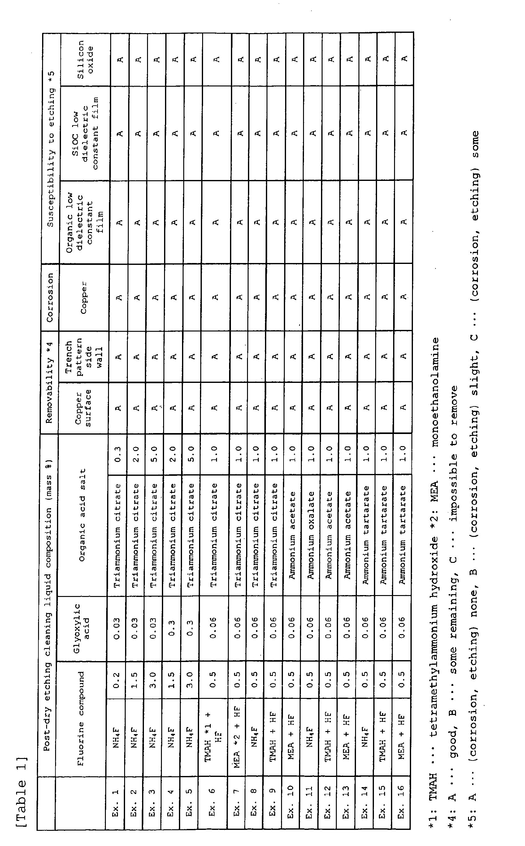
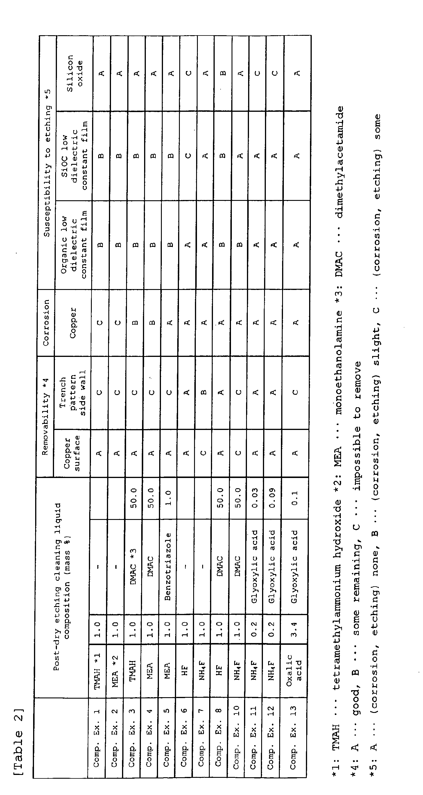
- Cleaning posttreatment for dry etching was carried out using cleaning liquid compositions of Examples and cleaning liquid compositions of Comparative Examples corresponding to these Examples, and removal characteristics of a polymer residue, corrosion of a metal material, and susceptibility to etching of an insulating film were evaluated.
- the etching characteristics of the cleaning liquid composition toward a low dielectric constant film were evaluated.
- a substrate that had been subjected to an ashing treatment after dry etching was subjected to a cleaning posttreatment using cleaning liquid compositions of each of the Examples and the corresponding Comparative Examples, and the removal characteristics of a photoresist residue, corrosion of a metal material, and susceptibility to etching of an insulating film were evaluated.
Landscapes
- Chemical & Material Sciences (AREA)
- Organic Chemistry (AREA)
- Engineering & Computer Science (AREA)
- Chemical Kinetics & Catalysis (AREA)
- Oil, Petroleum & Natural Gas (AREA)
- Wood Science & Technology (AREA)
- Life Sciences & Earth Sciences (AREA)
- Inorganic Chemistry (AREA)
- Emergency Medicine (AREA)
- Health & Medical Sciences (AREA)
- General Chemical & Material Sciences (AREA)
- Materials Engineering (AREA)
- Mechanical Engineering (AREA)
- Metallurgy (AREA)
- Cleaning Or Drying Semiconductors (AREA)
- Internal Circuitry In Semiconductor Integrated Circuit Devices (AREA)
- Insulated Gate Type Field-Effect Transistor (AREA)
- Drying Of Semiconductors (AREA)
Abstract
Description


Claims (13)
- A post-dry etching cleaning liquid composition for cleaning a substrate after dry etching, the composition comprising at least one type of fluorine compound, glyoxylic acid, at least one type of organic acid salt, and water.
- The post-dry etching cleaning liquid composition according to Claim 1, wherein the fluorine compound is ammonium fluoride.
- The post-dry etching cleaning liquid composition according to either Claim 1 or Claim 2, wherein the organic acid salt is at least one of ammonium oxalate, ammonium tartarate, ammonium citrate, and ammonium acetate.
- The post-dry etching cleaning liquid composition according to any one of Claims 1 to 3, wherein the cleaning liquid composition further comprises a surfactant.
- The post-dry etching cleaning liquid composition according to any one of Claims 1 to 4, wherein the cleaning liquid composition contains no organic solvent.
- The post-dry etching cleaning liquid composition according to any one of Claims 1 to 5, wherein the cleaning liquid composition is used for cleaning a substrate in which a wiring material formed from at least one of copper and a copper alloy and an interlayer insulating film formed from at least one of a low dielectric constant film and silicon oxide are exposed by dry etching.
- A process for fabricating a semiconductor device, the process comprising:a step of cleaning, using the post-dry etching cleaning liquid composition according to any one of Claims 1 to 6, a substrate that has been subjected to ashing removal of a mask pattern after dry etching through the mask pattern.
- A process for fabricating a semiconductor device, the process comprising:a step of patterning an insulating film formed above a substrate by dry etching through a mask pattern formed on the insulating film; anda step of cleaning, as a post-patterning treatment using a post-dry etching cleaning liquid composition, the substrate that has been subjected to the patterning of the insulating film, the cleaning liquid composition comprising at least one type of fluorine compound, glyoxylic acid, at least one type of organic acid salt, and water.
- The process for fabricating a semiconductor device according to Claim 8, wherein the insulating film is formed using a low dielectric constant material.
- The process for fabricating a semiconductor device according to Claim 8, wherein the insulating film is formed from a low dielectric constant film with an inorganic material film thereon.
- The process for fabricating a semiconductor device according to Claim 8, wherein the mask pattern is formed from an inorganic material.
- The process for fabricating a semiconductor device according to Claim 8, wherein a metal material layer beneath the insulating film is exposed by patterning of the insulating film.
- The process for fabricating a semiconductor device according to Claim 8, wherein after the cleaning step an inner wall of a trench pattern formed by patterning of the insulating film is covered by a conductive thin film, and a conductive material is embedded within the trench pattern via the conductive thin film.
Applications Claiming Priority (2)
| Application Number | Priority Date | Filing Date | Title |
|---|---|---|---|
| JP2004166571A JP2005347587A (en) | 2004-06-04 | 2004-06-04 | Cleaning liquid composition after dry etching and method for manufacturing semiconductor device |
| JP2004166571 | 2004-06-04 |
Publications (2)
| Publication Number | Publication Date |
|---|---|
| EP1602714A1 true EP1602714A1 (en) | 2005-12-07 |
| EP1602714B1 EP1602714B1 (en) | 2007-03-07 |
Family
ID=34937244
Family Applications (1)
| Application Number | Title | Priority Date | Filing Date |
|---|---|---|---|
| EP05012100A Expired - Lifetime EP1602714B1 (en) | 2004-06-04 | 2005-06-04 | Post-dry etching cleaning liquid composition and process for fabricating semiconductor device |
Country Status (7)
| Country | Link |
|---|---|
| US (3) | US20060019201A1 (en) |
| EP (1) | EP1602714B1 (en) |
| JP (1) | JP2005347587A (en) |
| KR (1) | KR20060048205A (en) |
| CN (1) | CN100529039C (en) |
| DE (1) | DE602005000657T2 (en) |
| TW (1) | TWI407489B (en) |
Families Citing this family (24)
| Publication number | Priority date | Publication date | Assignee | Title |
|---|---|---|---|---|
| US7316603B2 (en) * | 2002-01-22 | 2008-01-08 | Cabot Microelectronics Corporation | Compositions and methods for tantalum CMP |
| JP4456424B2 (en) * | 2004-06-29 | 2010-04-28 | 関東化学株式会社 | Photoresist residue and polymer residue removal composition |
| KR100827435B1 (en) * | 2006-01-31 | 2008-05-06 | 삼성전자주식회사 | Gate Forming Method Using Oxygen-free Ashing Process in Semiconductor Devices |
| CN101410954B (en) * | 2006-03-27 | 2010-06-02 | 东京毅力科创株式会社 | Method of substrate treatment, process for producing semiconductor device |
| KR101101104B1 (en) | 2006-08-24 | 2012-01-03 | 다이킨 고교 가부시키가이샤 | Residue removal liquid after semiconductor drying process and residue removal method using the same |
| US8685909B2 (en) | 2006-09-21 | 2014-04-01 | Advanced Technology Materials, Inc. | Antioxidants for post-CMP cleaning formulations |
| US7879783B2 (en) | 2007-01-11 | 2011-02-01 | Air Products And Chemicals, Inc. | Cleaning composition for semiconductor substrates |
| DE102007006151B4 (en) * | 2007-02-07 | 2008-11-06 | Siltronic Ag | A method of reducing and homogenizing the thickness of a semiconductor layer located on the surface of an electrically insulating material |
| KR101622862B1 (en) * | 2007-05-17 | 2016-05-19 | 엔테그리스, 아이엔씨. | New antioxidants for post-cmp cleaning formulations |
| CN101785087A (en) * | 2007-08-22 | 2010-07-21 | 大金工业株式会社 | Residue removing liquid after semiconductor dry process and residue removing method using the same |
| US8551880B2 (en) * | 2007-11-01 | 2013-10-08 | Applied Materials, Inc. | Ammonia-based plasma treatment for metal fill in narrow features |
| US7687381B2 (en) * | 2008-03-19 | 2010-03-30 | Samsung Electronics Co., Ltd. | Method of forming electrical interconnects within insulating layers that form consecutive sidewalls including forming a reaction layer on the inner sidewall |
| WO2010024093A1 (en) | 2008-08-25 | 2010-03-04 | ダイキン工業株式会社 | Solution for removal of residue after semiconductor dry processing and residue removal method using same |
| KR101752684B1 (en) | 2008-10-21 | 2017-07-04 | 엔테그리스, 아이엔씨. | Copper cleaning and protection formulations |
| JP5573138B2 (en) * | 2009-12-09 | 2014-08-20 | 豊田合成株式会社 | Manufacturing method of semiconductor light emitting device |
| JP2013521646A (en) * | 2010-03-05 | 2013-06-10 | ラム リサーチ コーポレーション | Cleaning solution for sidewall polymer by damascene treatment |
| KR20130101193A (en) * | 2012-03-05 | 2013-09-13 | 삼성디스플레이 주식회사 | System and method for cleaning panel |
| US9012322B2 (en) * | 2013-04-05 | 2015-04-21 | Intermolecular, Inc. | Selective etching of copper and copper-barrier materials by an aqueous base solution with fluoride addition |
| CN104795311B (en) | 2014-01-21 | 2018-06-01 | 中芯国际集成电路制造(上海)有限公司 | The forming method of semiconductor devices |
| JP6493396B2 (en) * | 2014-05-02 | 2019-04-03 | 三菱瓦斯化学株式会社 | Semiconductor device cleaning liquid and cleaning method |
| JP7322704B2 (en) * | 2017-07-31 | 2023-08-08 | 三菱瓦斯化学株式会社 | Composition liquid that suppresses damage to cobalt, alumina, interlayer insulating film, and silicon nitride, and cleaning method using the same |
| US20230268223A1 (en) * | 2022-02-24 | 2023-08-24 | Taiwan Semiconductor Manufacturing Co., Ltd. | Semiconductor devices and methods of manufacture |
| JP7760429B2 (en) * | 2022-03-29 | 2025-10-27 | 株式会社フジミインコーポレーテッド | Surface treatment composition, surface treatment method, and method for manufacturing semiconductor substrate |
| JP7760430B2 (en) * | 2022-03-29 | 2025-10-27 | 株式会社フジミインコーポレーテッド | Surface treatment composition |
Citations (3)
| Publication number | Priority date | Publication date | Assignee | Title |
|---|---|---|---|---|
| EP1318432A1 (en) * | 2001-12-04 | 2003-06-11 | Kanto Kagaku Kabushiki Kaisha | Photoresist residue removing liquid composition |
| EP1347339A1 (en) * | 2002-03-22 | 2003-09-24 | Kanto Kagaku Kabushiki Kaisha | Photoresist residue remover composition |
| EP1363321A2 (en) * | 2002-05-16 | 2003-11-19 | Kanto Kagaku Kabushiki Kaisha | Post-CMP washing liquid composition |
Family Cites Families (10)
| Publication number | Priority date | Publication date | Assignee | Title |
|---|---|---|---|---|
| JP3074634B2 (en) * | 1994-03-28 | 2000-08-07 | 三菱瓦斯化学株式会社 | Stripping solution for photoresist and method for forming wiring pattern |
| JP3436221B2 (en) * | 1999-03-15 | 2003-08-11 | ソニー株式会社 | Manufacturing method of semiconductor device |
| US6589882B2 (en) * | 2001-10-24 | 2003-07-08 | Micron Technology, Inc. | Copper post-etch cleaning process |
| JP2003142443A (en) * | 2001-10-31 | 2003-05-16 | Nippon Zeon Co Ltd | Substrate cleaning method and rinsing liquid |
| US6773873B2 (en) * | 2002-03-25 | 2004-08-10 | Advanced Technology Materials, Inc. | pH buffered compositions useful for cleaning residue from semiconductor substrates |
| JP2003313594A (en) * | 2002-04-22 | 2003-11-06 | Nec Corp | Cleaning liquid and method for manufacturing semiconductor device |
| JP4443864B2 (en) * | 2002-07-12 | 2010-03-31 | 株式会社ルネサステクノロジ | Cleaning solution for removing resist or etching residue and method for manufacturing semiconductor device |
| TW200413522A (en) * | 2002-11-08 | 2004-08-01 | Sumitomo Chemical Co | Washing liquid for semiconductor substrate |
| JP2004342632A (en) * | 2003-05-13 | 2004-12-02 | Matsushita Electric Ind Co Ltd | Method for manufacturing semiconductor device |
| KR100536378B1 (en) | 2003-11-19 | 2005-12-12 | 기아자동차주식회사 | An ECS unit movement method for roll over preventing |
-
2004
- 2004-06-04 JP JP2004166571A patent/JP2005347587A/en active Pending
-
2005
- 2005-05-31 TW TW094117900A patent/TWI407489B/en not_active IP Right Cessation
- 2005-06-04 EP EP05012100A patent/EP1602714B1/en not_active Expired - Lifetime
- 2005-06-04 DE DE602005000657T patent/DE602005000657T2/en not_active Expired - Lifetime
- 2005-06-04 KR KR1020050048096A patent/KR20060048205A/en not_active Abandoned
- 2005-06-06 CN CNB2005100755873A patent/CN100529039C/en not_active Expired - Fee Related
- 2005-06-06 US US11/145,731 patent/US20060019201A1/en not_active Abandoned
-
2008
- 2008-03-11 US US12/075,578 patent/US20080188085A1/en not_active Abandoned
-
2010
- 2010-09-23 US US12/924,288 patent/US8513140B2/en not_active Expired - Fee Related
Patent Citations (3)
| Publication number | Priority date | Publication date | Assignee | Title |
|---|---|---|---|---|
| EP1318432A1 (en) * | 2001-12-04 | 2003-06-11 | Kanto Kagaku Kabushiki Kaisha | Photoresist residue removing liquid composition |
| EP1347339A1 (en) * | 2002-03-22 | 2003-09-24 | Kanto Kagaku Kabushiki Kaisha | Photoresist residue remover composition |
| EP1363321A2 (en) * | 2002-05-16 | 2003-11-19 | Kanto Kagaku Kabushiki Kaisha | Post-CMP washing liquid composition |
Also Published As
| Publication number | Publication date |
|---|---|
| US8513140B2 (en) | 2013-08-20 |
| US20110014793A1 (en) | 2011-01-20 |
| DE602005000657T2 (en) | 2007-11-29 |
| TWI407489B (en) | 2013-09-01 |
| EP1602714B1 (en) | 2007-03-07 |
| US20080188085A1 (en) | 2008-08-07 |
| CN1706925A (en) | 2005-12-14 |
| DE602005000657D1 (en) | 2007-04-19 |
| CN100529039C (en) | 2009-08-19 |
| JP2005347587A (en) | 2005-12-15 |
| KR20060048205A (en) | 2006-05-18 |
| US20060019201A1 (en) | 2006-01-26 |
| TW200603262A (en) | 2006-01-16 |
Similar Documents
| Publication | Publication Date | Title |
|---|---|---|
| US8513140B2 (en) | Post-dry etching cleaning liquid composition and process for fabricating semiconductor device | |
| TWI399621B (en) | Composition for removing photoresist residue and polymer residue | |
| US6869921B2 (en) | Stripping composition | |
| US6773873B2 (en) | pH buffered compositions useful for cleaning residue from semiconductor substrates | |
| EP2164938B1 (en) | New antioxidants for post-cmp cleaning formulations | |
| US8772214B2 (en) | Aqueous cleaning composition for removing residues and method using same | |
| TWI582230B (en) | A cleaning solution for a semiconductor element, and a cleaning method using the cleaning solution | |
| US20090131295A1 (en) | Compositions for Removal of Metal Hard Mask Etching Residues from a Semiconductor Substrate | |
| US6399552B1 (en) | Aqueous cleaning solution for removing contaminants surface of circuit substrate cleaning method using the same | |
| US20050003977A1 (en) | Composition for cleaning | |
| JP2007519942A (en) | Chemicals and methods for stripping resist, BARC, and gap fill materials | |
| US7816313B2 (en) | Photoresist residue remover composition and semiconductor circuit element production process employing the same | |
| CN1802731A (en) | Removal of post-etch residues in semiconductor processing | |
| TWI678601B (en) | Cleaning liquid for semiconductor element capable of suppressing damage of tungsten-containing material and method for cleaning semiconductor element using the cleaning liquid | |
| KR100946636B1 (en) | Photoresist residue removal composition | |
| JP3389166B2 (en) | Stripping composition for resist | |
| TWI416282B (en) | Composition for removing residual photoresist and polymer and residue removal process using the same | |
| CN113214920A (en) | Cleaning preparation | |
| TWI734149B (en) | Post etch residue cleaning compositions and methods of using the same | |
| KR20170084008A (en) | Semiconductor element cleaning solution that suppresses damage to tantalum-containing materials, and cleaning method using same | |
| US20060091355A1 (en) | Solution and method for removing ashing residue in Cu/low-k multilevel interconnection structure | |
| HK1149524A (en) | Compositions for removal of metal hard mask etching residues from a semiconductor substrate |
Legal Events
| Date | Code | Title | Description |
|---|---|---|---|
| PUAI | Public reference made under article 153(3) epc to a published international application that has entered the european phase |
Free format text: ORIGINAL CODE: 0009012 |
|
| AK | Designated contracting states |
Kind code of ref document: A1 Designated state(s): AT BE BG CH CY CZ DE DK EE ES FI FR GB GR HU IE IS IT LI LT LU MC NL PL PT RO SE SI SK TR |
|
| AX | Request for extension of the european patent |
Extension state: AL BA HR LV MK YU |
|
| 17P | Request for examination filed |
Effective date: 20060323 |
|
| GRAP | Despatch of communication of intention to grant a patent |
Free format text: ORIGINAL CODE: EPIDOSNIGR1 |
|
| AKX | Designation fees paid |
Designated state(s): DE FR GB IT |
|
| GRAS | Grant fee paid |
Free format text: ORIGINAL CODE: EPIDOSNIGR3 |
|
| GRAA | (expected) grant |
Free format text: ORIGINAL CODE: 0009210 |
|
| AK | Designated contracting states |
Kind code of ref document: B1 Designated state(s): DE FR GB IT |
|
| REG | Reference to a national code |
Ref country code: GB Ref legal event code: FG4D |
|
| REF | Corresponds to: |
Ref document number: 602005000657 Country of ref document: DE Date of ref document: 20070419 Kind code of ref document: P |
|
| ET | Fr: translation filed | ||
| PLBE | No opposition filed within time limit |
Free format text: ORIGINAL CODE: 0009261 |
|
| STAA | Information on the status of an ep patent application or granted ep patent |
Free format text: STATUS: NO OPPOSITION FILED WITHIN TIME LIMIT |
|
| 26N | No opposition filed |
Effective date: 20071210 |
|
| PGFP | Annual fee paid to national office [announced via postgrant information from national office to epo] |
Ref country code: GB Payment date: 20130619 Year of fee payment: 9 Ref country code: DE Payment date: 20130620 Year of fee payment: 9 |
|
| PGFP | Annual fee paid to national office [announced via postgrant information from national office to epo] |
Ref country code: FR Payment date: 20130703 Year of fee payment: 9 Ref country code: IT Payment date: 20130624 Year of fee payment: 9 |
|
| REG | Reference to a national code |
Ref country code: DE Ref legal event code: R119 Ref document number: 602005000657 Country of ref document: DE |
|
| GBPC | Gb: european patent ceased through non-payment of renewal fee |
Effective date: 20140604 |
|
| REG | Reference to a national code |
Ref country code: FR Ref legal event code: ST Effective date: 20150227 |
|
| REG | Reference to a national code |
Ref country code: DE Ref legal event code: R119 Ref document number: 602005000657 Country of ref document: DE Effective date: 20150101 |
|
| PG25 | Lapsed in a contracting state [announced via postgrant information from national office to epo] |
Ref country code: IT Free format text: LAPSE BECAUSE OF NON-PAYMENT OF DUE FEES Effective date: 20140604 Ref country code: DE Free format text: LAPSE BECAUSE OF NON-PAYMENT OF DUE FEES Effective date: 20150101 |
|
| PG25 | Lapsed in a contracting state [announced via postgrant information from national office to epo] |
Ref country code: FR Free format text: LAPSE BECAUSE OF NON-PAYMENT OF DUE FEES Effective date: 20140630 Ref country code: GB Free format text: LAPSE BECAUSE OF NON-PAYMENT OF DUE FEES Effective date: 20140604 |