EP1601629B1 - Ferromagnetic material - Google Patents
Ferromagnetic material Download PDFInfo
- Publication number
- EP1601629B1 EP1601629B1 EP04708955A EP04708955A EP1601629B1 EP 1601629 B1 EP1601629 B1 EP 1601629B1 EP 04708955 A EP04708955 A EP 04708955A EP 04708955 A EP04708955 A EP 04708955A EP 1601629 B1 EP1601629 B1 EP 1601629B1
- Authority
- EP
- European Patent Office
- Prior art keywords
- temperature
- ferromagnetic
- kelvin
- doped zno
- zno
- Prior art date
- Legal status (The legal status is an assumption and is not a legal conclusion. Google has not performed a legal analysis and makes no representation as to the accuracy of the status listed.)
- Expired - Lifetime
Links
- 239000003302 ferromagnetic material Substances 0.000 title description 4
- 239000011572 manganese Substances 0.000 claims abstract description 65
- 239000000463 material Substances 0.000 claims abstract description 44
- 230000005294 ferromagnetic effect Effects 0.000 claims abstract description 32
- 229910052748 manganese Inorganic materials 0.000 claims abstract description 22
- 239000004065 semiconductor Substances 0.000 claims abstract description 19
- PWHULOQIROXLJO-UHFFFAOYSA-N Manganese Chemical compound [Mn] PWHULOQIROXLJO-UHFFFAOYSA-N 0.000 claims abstract description 12
- 238000000034 method Methods 0.000 claims abstract description 10
- 239000000758 substrate Substances 0.000 claims description 13
- 238000005245 sintering Methods 0.000 claims description 10
- NUJOXMJBOLGQSY-UHFFFAOYSA-N manganese dioxide Chemical compound O=[Mn]=O NUJOXMJBOLGQSY-UHFFFAOYSA-N 0.000 claims description 8
- 238000004544 sputter deposition Methods 0.000 claims description 8
- 239000011701 zinc Substances 0.000 claims description 8
- VYPSYNLAJGMNEJ-UHFFFAOYSA-N Silicium dioxide Chemical compound O=[Si]=O VYPSYNLAJGMNEJ-UHFFFAOYSA-N 0.000 claims description 6
- 238000000151 deposition Methods 0.000 claims description 6
- 230000008021 deposition Effects 0.000 claims description 6
- 239000005350 fused silica glass Substances 0.000 claims description 6
- 239000000203 mixture Substances 0.000 claims description 6
- 230000003287 optical effect Effects 0.000 claims description 6
- 239000000843 powder Substances 0.000 claims description 6
- 238000004519 manufacturing process Methods 0.000 claims description 5
- 239000010409 thin film Substances 0.000 claims description 5
- HCHKCACWOHOZIP-UHFFFAOYSA-N Zinc Chemical compound [Zn] HCHKCACWOHOZIP-UHFFFAOYSA-N 0.000 claims description 4
- 239000000919 ceramic Substances 0.000 claims description 4
- 238000004549 pulsed laser deposition Methods 0.000 claims description 4
- 229910052725 zinc Inorganic materials 0.000 claims description 4
- 239000002105 nanoparticle Substances 0.000 claims description 3
- 239000002245 particle Substances 0.000 claims description 2
- 239000013590 bulk material Substances 0.000 claims 3
- 238000001354 calcination Methods 0.000 claims 2
- WPBNNNQJVZRUHP-UHFFFAOYSA-L manganese(2+);methyl n-[[2-(methoxycarbonylcarbamothioylamino)phenyl]carbamothioyl]carbamate;n-[2-(sulfidocarbothioylamino)ethyl]carbamodithioate Chemical compound [Mn+2].[S-]C(=S)NCCNC([S-])=S.COC(=O)NC(=S)NC1=CC=CC=C1NC(=S)NC(=O)OC WPBNNNQJVZRUHP-UHFFFAOYSA-L 0.000 claims 1
- XLOMVQKBTHCTTD-UHFFFAOYSA-N Zinc monoxide Chemical compound [Zn]=O XLOMVQKBTHCTTD-UHFFFAOYSA-N 0.000 abstract description 62
- 239000011787 zinc oxide Substances 0.000 abstract description 30
- 239000010408 film Substances 0.000 description 16
- 230000005307 ferromagnetism Effects 0.000 description 15
- 230000005291 magnetic effect Effects 0.000 description 15
- 239000008188 pellet Substances 0.000 description 7
- 230000005350 ferromagnetic resonance Effects 0.000 description 6
- 230000005298 paramagnetic effect Effects 0.000 description 6
- 238000002474 experimental method Methods 0.000 description 5
- 230000005323 ferromagnetic ordering Effects 0.000 description 5
- XEEYBQQBJWHFJM-UHFFFAOYSA-N Iron Chemical compound [Fe] XEEYBQQBJWHFJM-UHFFFAOYSA-N 0.000 description 4
- 230000015654 memory Effects 0.000 description 4
- 238000001228 spectrum Methods 0.000 description 4
- JBRZTFJDHDCESZ-UHFFFAOYSA-N AsGa Chemical compound [As]#[Ga] JBRZTFJDHDCESZ-UHFFFAOYSA-N 0.000 description 3
- 238000004364 calculation method Methods 0.000 description 3
- 238000013461 design Methods 0.000 description 3
- 230000006870 function Effects 0.000 description 3
- 229910001218 Gallium arsenide Inorganic materials 0.000 description 2
- PXHVJJICTQNCMI-UHFFFAOYSA-N Nickel Chemical compound [Ni] PXHVJJICTQNCMI-UHFFFAOYSA-N 0.000 description 2
- GWEVSGVZZGPLCZ-UHFFFAOYSA-N Titan oxide Chemical compound O=[Ti]=O GWEVSGVZZGPLCZ-UHFFFAOYSA-N 0.000 description 2
- 238000005263 ab initio calculation Methods 0.000 description 2
- 230000005290 antiferromagnetic effect Effects 0.000 description 2
- 230000006399 behavior Effects 0.000 description 2
- 230000005292 diamagnetic effect Effects 0.000 description 2
- 230000000694 effects Effects 0.000 description 2
- 229910052742 iron Inorganic materials 0.000 description 2
- 238000013507 mapping Methods 0.000 description 2
- 238000005457 optimization Methods 0.000 description 2
- 238000012552 review Methods 0.000 description 2
- 238000000087 superconducting quantum interference device magnetometry Methods 0.000 description 2
- 229960001296 zinc oxide Drugs 0.000 description 2
- 235000014692 zinc oxide Nutrition 0.000 description 2
- 229910002601 GaN Inorganic materials 0.000 description 1
- 102100021164 Vasodilator-stimulated phosphoprotein Human genes 0.000 description 1
- 238000002441 X-ray diffraction Methods 0.000 description 1
- 229910045601 alloy Inorganic materials 0.000 description 1
- 239000000956 alloy Substances 0.000 description 1
- 238000004458 analytical method Methods 0.000 description 1
- 238000013459 approach Methods 0.000 description 1
- 230000015572 biosynthetic process Effects 0.000 description 1
- 239000000969 carrier Substances 0.000 description 1
- 229910017052 cobalt Inorganic materials 0.000 description 1
- 239000010941 cobalt Substances 0.000 description 1
- GUTLYIVDDKVIGB-UHFFFAOYSA-N cobalt atom Chemical compound [Co] GUTLYIVDDKVIGB-UHFFFAOYSA-N 0.000 description 1
- 230000008878 coupling Effects 0.000 description 1
- 238000010168 coupling process Methods 0.000 description 1
- 238000005859 coupling reaction Methods 0.000 description 1
- 238000009826 distribution Methods 0.000 description 1
- 238000001362 electron spin resonance spectrum Methods 0.000 description 1
- 238000005516 engineering process Methods 0.000 description 1
- 230000001747 exhibiting effect Effects 0.000 description 1
- 239000003574 free electron Substances 0.000 description 1
- 239000007789 gas Substances 0.000 description 1
- 238000010348 incorporation Methods 0.000 description 1
- 238000000608 laser ablation Methods 0.000 description 1
- 230000005415 magnetization Effects 0.000 description 1
- 238000005259 measurement Methods 0.000 description 1
- 229910052759 nickel Inorganic materials 0.000 description 1
- 239000000382 optic material Substances 0.000 description 1
- 230000000737 periodic effect Effects 0.000 description 1
- 239000002243 precursor Substances 0.000 description 1
- 238000005070 sampling Methods 0.000 description 1
- 230000005328 spin glass Effects 0.000 description 1
- 230000002277 temperature effect Effects 0.000 description 1
- 239000010936 titanium Substances 0.000 description 1
- 229910052723 transition metal Inorganic materials 0.000 description 1
- 238000009827 uniform distribution Methods 0.000 description 1
Images


Classifications
-
- C—CHEMISTRY; METALLURGY
- C04—CEMENTS; CONCRETE; ARTIFICIAL STONE; CERAMICS; REFRACTORIES
- C04B—LIME, MAGNESIA; SLAG; CEMENTS; COMPOSITIONS THEREOF, e.g. MORTARS, CONCRETE OR LIKE BUILDING MATERIALS; ARTIFICIAL STONE; CERAMICS; REFRACTORIES; TREATMENT OF NATURAL STONE
- C04B35/00—Shaped ceramic products characterised by their composition; Ceramics compositions; Processing powders of inorganic compounds preparatory to the manufacturing of ceramic products
- C04B35/01—Shaped ceramic products characterised by their composition; Ceramics compositions; Processing powders of inorganic compounds preparatory to the manufacturing of ceramic products based on oxide ceramics
- C04B35/453—Shaped ceramic products characterised by their composition; Ceramics compositions; Processing powders of inorganic compounds preparatory to the manufacturing of ceramic products based on oxide ceramics based on zinc, tin, or bismuth oxides or solid solutions thereof with other oxides, e.g. zincates, stannates or bismuthates
-
- H—ELECTRICITY
- H01—ELECTRIC ELEMENTS
- H01F—MAGNETS; INDUCTANCES; TRANSFORMERS; SELECTION OF MATERIALS FOR THEIR MAGNETIC PROPERTIES
- H01F41/00—Apparatus or processes specially adapted for manufacturing or assembling magnets, inductances or transformers; Apparatus or processes specially adapted for manufacturing materials characterised by their magnetic properties
- H01F41/14—Apparatus or processes specially adapted for manufacturing or assembling magnets, inductances or transformers; Apparatus or processes specially adapted for manufacturing materials characterised by their magnetic properties for applying magnetic films to substrates
- H01F41/20—Apparatus or processes specially adapted for manufacturing or assembling magnets, inductances or transformers; Apparatus or processes specially adapted for manufacturing materials characterised by their magnetic properties for applying magnetic films to substrates by evaporation
- H01F41/205—Apparatus or processes specially adapted for manufacturing or assembling magnets, inductances or transformers; Apparatus or processes specially adapted for manufacturing materials characterised by their magnetic properties for applying magnetic films to substrates by evaporation by laser ablation, e.g. pulsed laser deposition [PLD]
-
- B—PERFORMING OPERATIONS; TRANSPORTING
- B82—NANOTECHNOLOGY
- B82Y—SPECIFIC USES OR APPLICATIONS OF NANOSTRUCTURES; MEASUREMENT OR ANALYSIS OF NANOSTRUCTURES; MANUFACTURE OR TREATMENT OF NANOSTRUCTURES
- B82Y25/00—Nanomagnetism, e.g. magnetoimpedance, anisotropic magnetoresistance, giant magnetoresistance or tunneling magnetoresistance
-
- H—ELECTRICITY
- H01—ELECTRIC ELEMENTS
- H01F—MAGNETS; INDUCTANCES; TRANSFORMERS; SELECTION OF MATERIALS FOR THEIR MAGNETIC PROPERTIES
- H01F1/00—Magnets or magnetic bodies characterised by the magnetic materials therefor; Selection of materials for their magnetic properties
- H01F1/0036—Magnets or magnetic bodies characterised by the magnetic materials therefor; Selection of materials for their magnetic properties showing low dimensional magnetism, i.e. spin rearrangements due to a restriction of dimensions, e.g. showing giant magnetoresistivity
- H01F1/0045—Zero dimensional, e.g. nanoparticles, soft nanoparticles for medical/biological use
-
- H—ELECTRICITY
- H01—ELECTRIC ELEMENTS
- H01F—MAGNETS; INDUCTANCES; TRANSFORMERS; SELECTION OF MATERIALS FOR THEIR MAGNETIC PROPERTIES
- H01F1/00—Magnets or magnetic bodies characterised by the magnetic materials therefor; Selection of materials for their magnetic properties
- H01F1/01—Magnets or magnetic bodies characterised by the magnetic materials therefor; Selection of materials for their magnetic properties of inorganic materials
- H01F1/40—Magnets or magnetic bodies characterised by the magnetic materials therefor; Selection of materials for their magnetic properties of inorganic materials of magnetic semiconductor materials, e.g. CdCr2S4
- H01F1/401—Magnets or magnetic bodies characterised by the magnetic materials therefor; Selection of materials for their magnetic properties of inorganic materials of magnetic semiconductor materials, e.g. CdCr2S4 diluted
-
- H—ELECTRICITY
- H01—ELECTRIC ELEMENTS
- H01F—MAGNETS; INDUCTANCES; TRANSFORMERS; SELECTION OF MATERIALS FOR THEIR MAGNETIC PROPERTIES
- H01F1/00—Magnets or magnetic bodies characterised by the magnetic materials therefor; Selection of materials for their magnetic properties
- H01F1/01—Magnets or magnetic bodies characterised by the magnetic materials therefor; Selection of materials for their magnetic properties of inorganic materials
- H01F1/40—Magnets or magnetic bodies characterised by the magnetic materials therefor; Selection of materials for their magnetic properties of inorganic materials of magnetic semiconductor materials, e.g. CdCr2S4
- H01F1/401—Magnets or magnetic bodies characterised by the magnetic materials therefor; Selection of materials for their magnetic properties of inorganic materials of magnetic semiconductor materials, e.g. CdCr2S4 diluted
- H01F1/402—Magnets or magnetic bodies characterised by the magnetic materials therefor; Selection of materials for their magnetic properties of inorganic materials of magnetic semiconductor materials, e.g. CdCr2S4 diluted of II-VI type, e.g. Zn1-x Crx Se
-
- H—ELECTRICITY
- H01—ELECTRIC ELEMENTS
- H01F—MAGNETS; INDUCTANCES; TRANSFORMERS; SELECTION OF MATERIALS FOR THEIR MAGNETIC PROPERTIES
- H01F10/00—Thin magnetic films, e.g. of one-domain structure
- H01F10/08—Thin magnetic films, e.g. of one-domain structure characterised by magnetic layers
- H01F10/10—Thin magnetic films, e.g. of one-domain structure characterised by magnetic layers characterised by the composition
-
- H—ELECTRICITY
- H01—ELECTRIC ELEMENTS
- H01F—MAGNETS; INDUCTANCES; TRANSFORMERS; SELECTION OF MATERIALS FOR THEIR MAGNETIC PROPERTIES
- H01F10/00—Thin magnetic films, e.g. of one-domain structure
- H01F10/08—Thin magnetic films, e.g. of one-domain structure characterised by magnetic layers
- H01F10/10—Thin magnetic films, e.g. of one-domain structure characterised by magnetic layers characterised by the composition
- H01F10/18—Thin magnetic films, e.g. of one-domain structure characterised by magnetic layers characterised by the composition being compounds
- H01F10/193—Magnetic semiconductor compounds
-
- H—ELECTRICITY
- H01—ELECTRIC ELEMENTS
- H01F—MAGNETS; INDUCTANCES; TRANSFORMERS; SELECTION OF MATERIALS FOR THEIR MAGNETIC PROPERTIES
- H01F41/00—Apparatus or processes specially adapted for manufacturing or assembling magnets, inductances or transformers; Apparatus or processes specially adapted for manufacturing materials characterised by their magnetic properties
- H01F41/02—Apparatus or processes specially adapted for manufacturing or assembling magnets, inductances or transformers; Apparatus or processes specially adapted for manufacturing materials characterised by their magnetic properties for manufacturing cores, coils, or magnets
- H01F41/0206—Manufacturing of magnetic cores by mechanical means
- H01F41/0246—Manufacturing of magnetic circuits by moulding or by pressing powder
-
- H—ELECTRICITY
- H01—ELECTRIC ELEMENTS
- H01F—MAGNETS; INDUCTANCES; TRANSFORMERS; SELECTION OF MATERIALS FOR THEIR MAGNETIC PROPERTIES
- H01F41/00—Apparatus or processes specially adapted for manufacturing or assembling magnets, inductances or transformers; Apparatus or processes specially adapted for manufacturing materials characterised by their magnetic properties
- H01F41/14—Apparatus or processes specially adapted for manufacturing or assembling magnets, inductances or transformers; Apparatus or processes specially adapted for manufacturing materials characterised by their magnetic properties for applying magnetic films to substrates
- H01F41/18—Apparatus or processes specially adapted for manufacturing or assembling magnets, inductances or transformers; Apparatus or processes specially adapted for manufacturing materials characterised by their magnetic properties for applying magnetic films to substrates by cathode sputtering
-
- H—ELECTRICITY
- H10—SEMICONDUCTOR DEVICES; ELECTRIC SOLID-STATE DEVICES NOT OTHERWISE PROVIDED FOR
- H10N—ELECTRIC SOLID-STATE DEVICES NOT OTHERWISE PROVIDED FOR
- H10N50/00—Galvanomagnetic devices
- H10N50/80—Constructional details
- H10N50/85—Materials of the active region
-
- B—PERFORMING OPERATIONS; TRANSPORTING
- B82—NANOTECHNOLOGY
- B82Y—SPECIFIC USES OR APPLICATIONS OF NANOSTRUCTURES; MEASUREMENT OR ANALYSIS OF NANOSTRUCTURES; MANUFACTURE OR TREATMENT OF NANOSTRUCTURES
- B82Y30/00—Nanotechnology for materials or surface science, e.g. nanocomposites
-
- C—CHEMISTRY; METALLURGY
- C04—CEMENTS; CONCRETE; ARTIFICIAL STONE; CERAMICS; REFRACTORIES
- C04B—LIME, MAGNESIA; SLAG; CEMENTS; COMPOSITIONS THEREOF, e.g. MORTARS, CONCRETE OR LIKE BUILDING MATERIALS; ARTIFICIAL STONE; CERAMICS; REFRACTORIES; TREATMENT OF NATURAL STONE
- C04B2235/00—Aspects relating to ceramic starting mixtures or sintered ceramic products
- C04B2235/02—Composition of constituents of the starting material or of secondary phases of the final product
- C04B2235/30—Constituents and secondary phases not being of a fibrous nature
- C04B2235/32—Metal oxides, mixed metal oxides, or oxide-forming salts thereof, e.g. carbonates, nitrates, (oxy)hydroxides, chlorides
- C04B2235/3262—Manganese oxides, manganates, rhenium oxides or oxide-forming salts thereof, e.g. MnO
- C04B2235/3267—MnO2
-
- C—CHEMISTRY; METALLURGY
- C04—CEMENTS; CONCRETE; ARTIFICIAL STONE; CERAMICS; REFRACTORIES
- C04B—LIME, MAGNESIA; SLAG; CEMENTS; COMPOSITIONS THEREOF, e.g. MORTARS, CONCRETE OR LIKE BUILDING MATERIALS; ARTIFICIAL STONE; CERAMICS; REFRACTORIES; TREATMENT OF NATURAL STONE
- C04B2235/00—Aspects relating to ceramic starting mixtures or sintered ceramic products
- C04B2235/02—Composition of constituents of the starting material or of secondary phases of the final product
- C04B2235/30—Constituents and secondary phases not being of a fibrous nature
- C04B2235/32—Metal oxides, mixed metal oxides, or oxide-forming salts thereof, e.g. carbonates, nitrates, (oxy)hydroxides, chlorides
- C04B2235/3284—Zinc oxides, zincates, cadmium oxides, cadmiates, mercury oxides, mercurates or oxide forming salts thereof
-
- C—CHEMISTRY; METALLURGY
- C04—CEMENTS; CONCRETE; ARTIFICIAL STONE; CERAMICS; REFRACTORIES
- C04B—LIME, MAGNESIA; SLAG; CEMENTS; COMPOSITIONS THEREOF, e.g. MORTARS, CONCRETE OR LIKE BUILDING MATERIALS; ARTIFICIAL STONE; CERAMICS; REFRACTORIES; TREATMENT OF NATURAL STONE
- C04B2235/00—Aspects relating to ceramic starting mixtures or sintered ceramic products
- C04B2235/70—Aspects relating to sintered or melt-casted ceramic products
- C04B2235/96—Properties of ceramic products, e.g. mechanical properties such as strength, toughness, wear resistance
- C04B2235/9646—Optical properties
- C04B2235/9653—Translucent or transparent ceramics other than alumina
-
- H—ELECTRICITY
- H01—ELECTRIC ELEMENTS
- H01F—MAGNETS; INDUCTANCES; TRANSFORMERS; SELECTION OF MATERIALS FOR THEIR MAGNETIC PROPERTIES
- H01F1/00—Magnets or magnetic bodies characterised by the magnetic materials therefor; Selection of materials for their magnetic properties
- H01F1/0009—Antiferromagnetic materials, i.e. materials exhibiting a Néel transition temperature
-
- H—ELECTRICITY
- H10—SEMICONDUCTOR DEVICES; ELECTRIC SOLID-STATE DEVICES NOT OTHERWISE PROVIDED FOR
- H10N—ELECTRIC SOLID-STATE DEVICES NOT OTHERWISE PROVIDED FOR
- H10N30/00—Piezoelectric or electrostrictive devices
- H10N30/80—Constructional details
- H10N30/85—Piezoelectric or electrostrictive active materials
- H10N30/853—Ceramic compositions
Definitions
- the present invention relates to materials used for electronic components which use ferromagnetism in its function.
- Components based on materials with ferromagnetic properties are devised to affect or rectify the spin orientation of bosons and fermions, e.g. electrons.
- the search for materials with ferromagnetism above room temperatures in dilute magnetic semiconductors has been a quest in recent years, especially to develop a potentially rich new class of future devices which exploit the electron spin state i.e. spintronics.
- the types of components for these devices include magnetic memories, e.g. hard discs, semiconductor magnetic memories, e.g. MRAM, spin valve transistors, spin light emitting diodes, non-volatile memory, logic devices, quantum computers, optical isolators, sensors, ultra-fast optical switches etc.
- Dilute magnetic semiconductors can also be used in electronic-, and magnetic -based products.
- Spintronic devices such as spin valve transistors, spin light emitting diodes, non-volatile memory, logic devices, optical isolators and ultra-fast optical switches are some of the areas of high interest for introducing the ferromagnetic properties at room temperature in a semiconductor described in the two documents of reference 6 and 7.
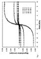
- the present invention is based on the concept to create ferromagnetism into doped dilute magnetic semiconductors by doping Zinc Oxide (ZnO) with Manganese (Mn). Tailoring of ferromagnetism above room temperature in bulk Mn ( ⁇ 4 atomic %) doped ZnO has been achieved. In this state Mn is found to carry a moment 0.16 ⁇ B . Ferromagnetic Resonance (FMR) data on these samples have confirmed the surprising results of the existence of ferromagnetic order at temperatures even as high as 425K. In the paramagnetic state the Paramagnetic Resonance data show that Mn is in the 2+ state (Mn 2+ ) with a g value 2.0029. Ab initio calculations confirm the above findings.
- Zinc Oxide Zinc Oxide
- Mn Manganese
- the ferromagnetism around room temperatures is completely suppressed giving rise to the often reported pronounced 'ferromagnetic-like' ordered state below 40K.
- the material also shows room temperature ferromagnetic ordering in 2-3 ⁇ m thick transparent films deposited on fused quartz substrates at temperatures below 600 °C by Pulsed Laser deposition using the same bulk materials as targets.
- the ferromagnetic dilute Mn doped ZnO can also be obtained as transparent nanoparticles.
- Manganese doped Zinc oxide with ferromagnetic properties in the specified temperature range can also be manufactured with a sputtering system where either two metallic (Zinc and Manganese) targets are used simultaneously or one sintered ZnO:Mn ceramic target.
- the present invention is based on the concept to create ferromagnetism in doped dilute magnetic semiconductors by doping Zinc Oxide (ZnO) with Manganese (Mn) in bulk or film materials.
- ZnO Zinc Oxide
- Mn Manganese
- Our experiments shows successful tailoring of ferromagnetism above room temperature in bulk Mn doped ZnO.
- the Mn doping level should then be less than 4-5 at% (atomic percent) for bulk materials.
- Theoretically we find that the upper limit for ferromagnetism is about 5 at% Mn.
- due to materials problems, above 4 at% Mn there is a clear tendency for the Mn atoms to form clusters which are then antiferromagnetic and that suppresses the ferromagnetic order.
- Room temperature ferromagnetic ordering has also been obtained in 2-3 ⁇ m thick films deposited on fused quartz substrates at temperatures below 600 °C, by Pulsed Laser deposition using the same bulk materials as targets.
- the doping concentration in these film materials should be less than 3-4at% in order to obtain controlled homogeneity.
- samples below 2 at% can be tailored to be homogeneous in composition with slight variations but containing no clusters.
- the substrate temperature effects the Mn concentration in the film. Films deposited at higher temperatures are found to have a high concentration of Mn in comparison to films deposited at low temperatures. This means that the temperature could be used to control the Mn concentration.
- the doped dilute semiconductor can also be processed, by particle size selection, into transparent and ferromagnetic nanoparticles.
- Manganese doped Zincoxide can be manufactured with a sputtering system where either two metallic (Zinc and Manganese) targets are used simultaneously or one sintered ZnO:Mn ceramic target as described previously.
- two metallic targets the sputtering energy on the Zn and Manganese targets are adjusted in such a way that the resulting Manganese content is in the 1-5% range.
- An exact recipe has to be adjusted to the sputtering equipment that is used and depends on energy, geometry and gases. This technique is, however, well known to the skilled person.
- the substrate temperature on the deposition substrate is in the same range as when using laser deposition.
Landscapes
- Engineering & Computer Science (AREA)
- Power Engineering (AREA)
- Chemical & Material Sciences (AREA)
- Manufacturing & Machinery (AREA)
- Ceramic Engineering (AREA)
- Nanotechnology (AREA)
- Materials Engineering (AREA)
- Structural Engineering (AREA)
- Organic Chemistry (AREA)
- Health & Medical Sciences (AREA)
- Molecular Biology (AREA)
- Optics & Photonics (AREA)
- Crystallography & Structural Chemistry (AREA)
- Life Sciences & Earth Sciences (AREA)
- Biomedical Technology (AREA)
- General Health & Medical Sciences (AREA)
- Physics & Mathematics (AREA)
- Hard Magnetic Materials (AREA)
- Compositions Of Oxide Ceramics (AREA)
- Developing Agents For Electrophotography (AREA)
- Valve Device For Special Equipments (AREA)
- Non-Silver Salt Photosensitive Materials And Non-Silver Salt Photography (AREA)
- Crystals, And After-Treatments Of Crystals (AREA)
- Thin Magnetic Films (AREA)
- Physical Vapour Deposition (AREA)
Applications Claiming Priority (3)
| Application Number | Priority Date | Filing Date | Title |
|---|---|---|---|
| SE0300352 | 2003-02-06 | ||
| SE0300352A SE0300352D0 (sv) | 2003-02-06 | 2003-02-06 | Ferromagnetism in semiconductors |
| PCT/SE2004/000150 WO2004069767A1 (en) | 2003-02-06 | 2004-02-06 | Ferromagnetic material |
Publications (2)
| Publication Number | Publication Date |
|---|---|
| EP1601629A1 EP1601629A1 (en) | 2005-12-07 |
| EP1601629B1 true EP1601629B1 (en) | 2008-05-14 |
Family
ID=20290360
Family Applications (1)
| Application Number | Title | Priority Date | Filing Date |
|---|---|---|---|
| EP04708955A Expired - Lifetime EP1601629B1 (en) | 2003-02-06 | 2004-02-06 | Ferromagnetic material |
Country Status (9)
| Country | Link |
|---|---|
| US (1) | US7527983B2 (enExample) |
| EP (1) | EP1601629B1 (enExample) |
| JP (1) | JP2006517175A (enExample) |
| KR (1) | KR20050110627A (enExample) |
| CN (1) | CN100430335C (enExample) |
| AT (1) | ATE395312T1 (enExample) |
| DE (1) | DE602004013735D1 (enExample) |
| SE (1) | SE0300352D0 (enExample) |
| WO (1) | WO2004069767A1 (enExample) |
Families Citing this family (7)
| Publication number | Priority date | Publication date | Assignee | Title |
|---|---|---|---|---|
| SE0300352D0 (sv) * | 2003-02-06 | 2003-02-06 | Winto Konsult Ab | Ferromagnetism in semiconductors |
| TWI237314B (en) * | 2004-06-24 | 2005-08-01 | Ind Tech Res Inst | Doping method for forming quantum dots |
| CN103194798B (zh) * | 2013-04-02 | 2015-08-26 | 浙江大学 | 一种过渡金属掺杂ZnO基铁磁多晶薄膜及其制备方法 |
| KR101661025B1 (ko) * | 2014-09-03 | 2016-09-29 | 한국세라믹기술원 | 반도성 세라믹스 조성물의 제조방법 및 그의 세라믹스 기판 |
| US9966901B2 (en) * | 2015-11-19 | 2018-05-08 | Samsung Electronics Co., Ltd. | Spin-torque oscillator based on easy-cone anisotropy |
| CN111809158A (zh) * | 2020-07-22 | 2020-10-23 | 延安大学 | 一种过渡金属掺杂ZnO纳米线阵列、制备方法及其应用 |
| CN113308669B (zh) * | 2021-04-26 | 2023-06-23 | 北京航空航天大学合肥创新研究院(北京航空航天大学合肥研究生院) | 一种Mn掺杂ZnO稀磁半导体薄膜的制备方法 |
Family Cites Families (8)
| Publication number | Priority date | Publication date | Assignee | Title |
|---|---|---|---|---|
| JP3953238B2 (ja) * | 1999-09-01 | 2007-08-08 | 独立行政法人科学技術振興機構 | 強磁性p型単結晶酸化亜鉛およびその製造方法 |
| JP4365495B2 (ja) * | 1999-10-29 | 2009-11-18 | ローム株式会社 | 遷移金属を含有する強磁性ZnO系化合物およびその強磁性特性の調整方法 |
| CN1313656C (zh) * | 2001-03-02 | 2007-05-02 | 独立行政法人科学技术振兴机构 | Ⅱ-ⅵ族或ⅲ-ⅴ族系单结晶铁磁性化合物及其铁磁性特性的调整方法 |
| JP2003298139A (ja) * | 2002-03-29 | 2003-10-17 | Alps Electric Co Ltd | 磁気検出素子 |
| SE0300352D0 (sv) * | 2003-02-06 | 2003-02-06 | Winto Konsult Ab | Ferromagnetism in semiconductors |
| SE528394C2 (sv) * | 2004-05-18 | 2006-11-07 | Nm Spintronics Ab | Mangandopade magnetiska halvledare |
| SE528900C2 (sv) * | 2004-05-18 | 2007-03-13 | Nm Spintronics Ab | Koppardopade magnetiska halvledare |
| JP2006139854A (ja) * | 2004-11-12 | 2006-06-01 | Sony Corp | 情報記録装置、情報記録方法 |
-
2003
- 2003-02-06 SE SE0300352A patent/SE0300352D0/xx unknown
-
2004
- 2004-02-06 JP JP2006502792A patent/JP2006517175A/ja active Pending
- 2004-02-06 CN CNB2004800049794A patent/CN100430335C/zh not_active Expired - Fee Related
- 2004-02-06 DE DE602004013735T patent/DE602004013735D1/de not_active Expired - Fee Related
- 2004-02-06 AT AT04708955T patent/ATE395312T1/de not_active IP Right Cessation
- 2004-02-06 US US10/544,655 patent/US7527983B2/en not_active Expired - Fee Related
- 2004-02-06 EP EP04708955A patent/EP1601629B1/en not_active Expired - Lifetime
- 2004-02-06 KR KR1020057014458A patent/KR20050110627A/ko not_active Ceased
- 2004-02-06 WO PCT/SE2004/000150 patent/WO2004069767A1/en not_active Ceased
Also Published As
| Publication number | Publication date |
|---|---|
| HK1093056A1 (zh) | 2007-02-23 |
| JP2006517175A (ja) | 2006-07-20 |
| EP1601629A1 (en) | 2005-12-07 |
| DE602004013735D1 (de) | 2008-06-26 |
| SE0300352D0 (sv) | 2003-02-06 |
| WO2004069767A1 (en) | 2004-08-19 |
| ATE395312T1 (de) | 2008-05-15 |
| KR20050110627A (ko) | 2005-11-23 |
| US20060148105A1 (en) | 2006-07-06 |
| CN1816503A (zh) | 2006-08-09 |
| US7527983B2 (en) | 2009-05-05 |
| CN100430335C (zh) | 2008-11-05 |
Similar Documents
| Publication | Publication Date | Title |
|---|---|---|
| Lin et al. | Enhancement of ferromagnetic properties in Zn1− xCoxO by additional Cu doping | |
| Davies et al. | Review of recent advances in transition and lanthanide metal–doped GaN and ZnO | |
| Chen et al. | Effects of temperature and atmosphere on the magnetism properties of Mn-doped ZnO | |
| US7527983B2 (en) | Ferromagnetic material | |
| US20070190367A1 (en) | Manganese Doped Magnetic Semiconductors | |
| Kamilla et al. | New semiconductor materials for magnetoelectronics at room temperature | |
| Sagar et al. | Synthesis and magnetic behaviour of Mn: ZnO nanocrystalline powders | |
| US8277960B2 (en) | Inhomogeneous compounds having high magnetic resistance, the production and use thereof | |
| US20080087972A1 (en) | Copper Doped Magnetic Semiconductors | |
| Cao et al. | The predicaments and expectations in development of magnetic semiconductors | |
| Jayakumar et al. | 5 Spintronic Materials, Synthesis | |
| HK1093056B (en) | Ferromagnetic material | |
| JP2008047624A (ja) | 反強磁性ハーフメタリック半導体 | |
| Lashkarev et al. | Diluted ferromagnetic semiconductors as spintronic materials | |
| Singhal et al. | Study of ferromagnetism in Mn doped ZnO dilute semiconductor system | |
| Jayashire et al. | Microstructural and Magnetic Property Investigations into Antiferromagnetic Mn2FeSi Heusler Alloy for Spintronics Applications | |
| López-Ponce et al. | Origin of room temperature magnetism in thin (ZnO) 1-x (MnO2) x films and ZnO/MnO2 multilayers | |
| Norton et al. | Transition Metal Doped ZnO | |
| HK1100721A (en) | Manganese doped magnetic semiconductors | |
| Norton et al. | Ferromagnetism in ZnO doped with transition metal ions | |
| Beleanu | Ternary lithium based compounds used for technological applications | |
| Pearton et al. | Transition metal doped ZnO for spintronics | |
| Park et al. | Physical Properties of Laser-Ablated La1− x SrxCoO3− δ Films | |
| Habermeier et al. | Cuprate based oxide superlattices showing simultaneously superconducting and ferromagnetic properties | |
| Yousong et al. | Theoretical prediction and experimental realization of transition metal doped rutiles as diluted magnetic semiconductors |
Legal Events
| Date | Code | Title | Description |
|---|---|---|---|
| PUAI | Public reference made under article 153(3) epc to a published international application that has entered the european phase |
Free format text: ORIGINAL CODE: 0009012 |
|
| 17P | Request for examination filed |
Effective date: 20050905 |
|
| AK | Designated contracting states |
Kind code of ref document: A1 Designated state(s): AT BE BG CH CY CZ DE DK EE ES FI FR GB GR HU IE IT LI LU MC NL PT RO SE SI SK TR |
|
| AX | Request for extension of the european patent |
Extension state: AL LT LV MK |
|
| DAX | Request for extension of the european patent (deleted) | ||
| 17Q | First examination report despatched |
Effective date: 20070410 |
|
| GRAP | Despatch of communication of intention to grant a patent |
Free format text: ORIGINAL CODE: EPIDOSNIGR1 |
|
| GRAS | Grant fee paid |
Free format text: ORIGINAL CODE: EPIDOSNIGR3 |
|
| GRAA | (expected) grant |
Free format text: ORIGINAL CODE: 0009210 |
|
| AK | Designated contracting states |
Kind code of ref document: B1 Designated state(s): AT BE BG CH CY CZ DE DK EE ES FI FR GB GR HU IE IT LI LU MC NL PT RO SE SI SK TR |
|
| REG | Reference to a national code |
Ref country code: GB Ref legal event code: FG4D |
|
| REG | Reference to a national code |
Ref country code: CH Ref legal event code: EP |
|
| RAP2 | Party data changed (patent owner data changed or rights of a patent transferred) |
Owner name: SPINTRONIX AB |
|
| REG | Reference to a national code |
Ref country code: IE Ref legal event code: FG4D Free format text: LANGUAGE OF EP DOCUMENT: FRENCH |
|
| REG | Reference to a national code |
Ref country code: CH Ref legal event code: NV Representative=s name: KIRKER & CIE S.A. |
|
| REF | Corresponds to: |
Ref document number: 602004013735 Country of ref document: DE Date of ref document: 20080626 Kind code of ref document: P |
|
| REG | Reference to a national code |
Ref country code: SE Ref legal event code: TRGR |
|
| REG | Reference to a national code |
Ref country code: CH Ref legal event code: NV Representative=s name: KIRKER & CIE S.A. |
|
| NLT2 | Nl: modifications (of names), taken from the european patent patent bulletin |
Owner name: SPINTRONIX AB Effective date: 20080611 |
|
| PG25 | Lapsed in a contracting state [announced via postgrant information from national office to epo] |
Ref country code: SI Free format text: LAPSE BECAUSE OF FAILURE TO SUBMIT A TRANSLATION OF THE DESCRIPTION OR TO PAY THE FEE WITHIN THE PRESCRIBED TIME-LIMIT Effective date: 20080514 |
|
| PG25 | Lapsed in a contracting state [announced via postgrant information from national office to epo] |
Ref country code: ES Free format text: LAPSE BECAUSE OF FAILURE TO SUBMIT A TRANSLATION OF THE DESCRIPTION OR TO PAY THE FEE WITHIN THE PRESCRIBED TIME-LIMIT Effective date: 20080825 |
|
| NLV1 | Nl: lapsed or annulled due to failure to fulfill the requirements of art. 29p and 29m of the patents act | ||
| PG25 | Lapsed in a contracting state [announced via postgrant information from national office to epo] |
Ref country code: NL Free format text: LAPSE BECAUSE OF FAILURE TO SUBMIT A TRANSLATION OF THE DESCRIPTION OR TO PAY THE FEE WITHIN THE PRESCRIBED TIME-LIMIT Effective date: 20080514 Ref country code: AT Free format text: LAPSE BECAUSE OF FAILURE TO SUBMIT A TRANSLATION OF THE DESCRIPTION OR TO PAY THE FEE WITHIN THE PRESCRIBED TIME-LIMIT Effective date: 20080514 |
|
| PG25 | Lapsed in a contracting state [announced via postgrant information from national office to epo] |
Ref country code: PT Free format text: LAPSE BECAUSE OF FAILURE TO SUBMIT A TRANSLATION OF THE DESCRIPTION OR TO PAY THE FEE WITHIN THE PRESCRIBED TIME-LIMIT Effective date: 20081014 Ref country code: DK Free format text: LAPSE BECAUSE OF FAILURE TO SUBMIT A TRANSLATION OF THE DESCRIPTION OR TO PAY THE FEE WITHIN THE PRESCRIBED TIME-LIMIT Effective date: 20080514 Ref country code: CZ Free format text: LAPSE BECAUSE OF FAILURE TO SUBMIT A TRANSLATION OF THE DESCRIPTION OR TO PAY THE FEE WITHIN THE PRESCRIBED TIME-LIMIT Effective date: 20080514 |
|
| PG25 | Lapsed in a contracting state [announced via postgrant information from national office to epo] |
Ref country code: RO Free format text: LAPSE BECAUSE OF FAILURE TO SUBMIT A TRANSLATION OF THE DESCRIPTION OR TO PAY THE FEE WITHIN THE PRESCRIBED TIME-LIMIT Effective date: 20080514 Ref country code: SK Free format text: LAPSE BECAUSE OF FAILURE TO SUBMIT A TRANSLATION OF THE DESCRIPTION OR TO PAY THE FEE WITHIN THE PRESCRIBED TIME-LIMIT Effective date: 20080514 Ref country code: BE Free format text: LAPSE BECAUSE OF FAILURE TO SUBMIT A TRANSLATION OF THE DESCRIPTION OR TO PAY THE FEE WITHIN THE PRESCRIBED TIME-LIMIT Effective date: 20080514 |
|
| PLBE | No opposition filed within time limit |
Free format text: ORIGINAL CODE: 0009261 |
|
| STAA | Information on the status of an ep patent application or granted ep patent |
Free format text: STATUS: NO OPPOSITION FILED WITHIN TIME LIMIT |
|
| REG | Reference to a national code |
Ref country code: FR Ref legal event code: CD Ref country code: FR Ref legal event code: CA |
|
| 26N | No opposition filed |
Effective date: 20090217 |
|
| PG25 | Lapsed in a contracting state [announced via postgrant information from national office to epo] |
Ref country code: BG Free format text: LAPSE BECAUSE OF FAILURE TO SUBMIT A TRANSLATION OF THE DESCRIPTION OR TO PAY THE FEE WITHIN THE PRESCRIBED TIME-LIMIT Effective date: 20080814 Ref country code: EE Free format text: LAPSE BECAUSE OF FAILURE TO SUBMIT A TRANSLATION OF THE DESCRIPTION OR TO PAY THE FEE WITHIN THE PRESCRIBED TIME-LIMIT Effective date: 20080514 |
|
| PG25 | Lapsed in a contracting state [announced via postgrant information from national office to epo] |
Ref country code: MC Free format text: LAPSE BECAUSE OF NON-PAYMENT OF DUE FEES Effective date: 20090228 |
|
| REG | Reference to a national code |
Ref country code: CH Ref legal event code: PL |
|
| EUG | Se: european patent has lapsed | ||
| GBPC | Gb: european patent ceased through non-payment of renewal fee |
Effective date: 20090206 |
|
| PG25 | Lapsed in a contracting state [announced via postgrant information from national office to epo] |
Ref country code: FI Free format text: LAPSE BECAUSE OF NON-PAYMENT OF DUE FEES Effective date: 20090206 Ref country code: LI Free format text: LAPSE BECAUSE OF NON-PAYMENT OF DUE FEES Effective date: 20090228 Ref country code: CH Free format text: LAPSE BECAUSE OF NON-PAYMENT OF DUE FEES Effective date: 20090228 |
|
| REG | Reference to a national code |
Ref country code: IE Ref legal event code: MM4A |
|
| REG | Reference to a national code |
Ref country code: FR Ref legal event code: ST Effective date: 20091030 |
|
| PG25 | Lapsed in a contracting state [announced via postgrant information from national office to epo] |
Ref country code: IE Free format text: LAPSE BECAUSE OF NON-PAYMENT OF DUE FEES Effective date: 20090206 Ref country code: DE Free format text: LAPSE BECAUSE OF NON-PAYMENT OF DUE FEES Effective date: 20090901 |
|
| PG25 | Lapsed in a contracting state [announced via postgrant information from national office to epo] |
Ref country code: GB Free format text: LAPSE BECAUSE OF NON-PAYMENT OF DUE FEES Effective date: 20090206 Ref country code: FR Free format text: LAPSE BECAUSE OF NON-PAYMENT OF DUE FEES Effective date: 20090302 |
|
| PG25 | Lapsed in a contracting state [announced via postgrant information from national office to epo] |
Ref country code: GR Free format text: LAPSE BECAUSE OF FAILURE TO SUBMIT A TRANSLATION OF THE DESCRIPTION OR TO PAY THE FEE WITHIN THE PRESCRIBED TIME-LIMIT Effective date: 20080815 |
|
| PG25 | Lapsed in a contracting state [announced via postgrant information from national office to epo] |
Ref country code: IT Free format text: LAPSE BECAUSE OF NON-PAYMENT OF DUE FEES Effective date: 20090206 |
|
| PG25 | Lapsed in a contracting state [announced via postgrant information from national office to epo] |
Ref country code: LU Free format text: LAPSE BECAUSE OF NON-PAYMENT OF DUE FEES Effective date: 20090206 |
|
| PG25 | Lapsed in a contracting state [announced via postgrant information from national office to epo] |
Ref country code: SE Free format text: LAPSE BECAUSE OF NON-PAYMENT OF DUE FEES Effective date: 20090207 |
|
| PG25 | Lapsed in a contracting state [announced via postgrant information from national office to epo] |
Ref country code: HU Free format text: LAPSE BECAUSE OF FAILURE TO SUBMIT A TRANSLATION OF THE DESCRIPTION OR TO PAY THE FEE WITHIN THE PRESCRIBED TIME-LIMIT Effective date: 20081115 |
|
| PG25 | Lapsed in a contracting state [announced via postgrant information from national office to epo] |
Ref country code: TR Free format text: LAPSE BECAUSE OF FAILURE TO SUBMIT A TRANSLATION OF THE DESCRIPTION OR TO PAY THE FEE WITHIN THE PRESCRIBED TIME-LIMIT Effective date: 20080514 |
|
| PG25 | Lapsed in a contracting state [announced via postgrant information from national office to epo] |
Ref country code: CY Free format text: LAPSE BECAUSE OF FAILURE TO SUBMIT A TRANSLATION OF THE DESCRIPTION OR TO PAY THE FEE WITHIN THE PRESCRIBED TIME-LIMIT Effective date: 20080514 |