EP1599803B1 - Cache-speicher-trashings-verringerung von bestimmten code-stücken - Google Patents
Cache-speicher-trashings-verringerung von bestimmten code-stücken Download PDFInfo
- Publication number
- EP1599803B1 EP1599803B1 EP04713597A EP04713597A EP1599803B1 EP 1599803 B1 EP1599803 B1 EP 1599803B1 EP 04713597 A EP04713597 A EP 04713597A EP 04713597 A EP04713597 A EP 04713597A EP 1599803 B1 EP1599803 B1 EP 1599803B1
- Authority
- EP
- European Patent Office
- Prior art keywords
- instruction
- cache
- instructions
- memory
- instruction data
- Prior art date
- Legal status (The legal status is an assumption and is not a legal conclusion. Google has not performed a legal analysis and makes no representation as to the accuracy of the status listed.)
- Expired - Lifetime
Links
Images


Classifications
-
- G—PHYSICS
- G06—COMPUTING OR CALCULATING; COUNTING
- G06F—ELECTRIC DIGITAL DATA PROCESSING
- G06F12/00—Accessing, addressing or allocating within memory systems or architectures
- G06F12/02—Addressing or allocation; Relocation
- G06F12/08—Addressing or allocation; Relocation in hierarchically structured memory systems, e.g. virtual memory systems
- G06F12/0802—Addressing of a memory level in which the access to the desired data or data block requires associative addressing means, e.g. caches
- G06F12/0875—Addressing of a memory level in which the access to the desired data or data block requires associative addressing means, e.g. caches with dedicated cache, e.g. instruction or stack
-
- G—PHYSICS
- G06—COMPUTING OR CALCULATING; COUNTING
- G06F—ELECTRIC DIGITAL DATA PROCESSING
- G06F12/00—Accessing, addressing or allocating within memory systems or architectures
- G06F12/02—Addressing or allocation; Relocation
- G06F12/08—Addressing or allocation; Relocation in hierarchically structured memory systems, e.g. virtual memory systems
- G06F12/0802—Addressing of a memory level in which the access to the desired data or data block requires associative addressing means, e.g. caches
- G06F12/0888—Addressing of a memory level in which the access to the desired data or data block requires associative addressing means, e.g. caches using selective caching, e.g. bypass
-
- G—PHYSICS
- G06—COMPUTING OR CALCULATING; COUNTING
- G06F—ELECTRIC DIGITAL DATA PROCESSING
- G06F12/00—Accessing, addressing or allocating within memory systems or architectures
- G06F12/02—Addressing or allocation; Relocation
- G06F12/08—Addressing or allocation; Relocation in hierarchically structured memory systems, e.g. virtual memory systems
- G06F12/0802—Addressing of a memory level in which the access to the desired data or data block requires associative addressing means, e.g. caches
- G06F12/0893—Caches characterised by their organisation or structure
- G06F12/0897—Caches characterised by their organisation or structure with two or more cache hierarchy levels
-
- G—PHYSICS
- G06—COMPUTING OR CALCULATING; COUNTING
- G06F—ELECTRIC DIGITAL DATA PROCESSING
- G06F9/00—Arrangements for program control, e.g. control units
- G06F9/06—Arrangements for program control, e.g. control units using stored programs, i.e. using an internal store of processing equipment to receive or retain programs
- G06F9/30—Arrangements for executing machine instructions, e.g. instruction decode
- G06F9/38—Concurrent instruction execution, e.g. pipeline or look ahead
- G06F9/3802—Instruction prefetching
- G06F9/3814—Implementation provisions of instruction buffers, e.g. prefetch buffer; banks
-
- G—PHYSICS
- G06—COMPUTING OR CALCULATING; COUNTING
- G06F—ELECTRIC DIGITAL DATA PROCESSING
- G06F9/00—Arrangements for program control, e.g. control units
- G06F9/06—Arrangements for program control, e.g. control units using stored programs, i.e. using an internal store of processing equipment to receive or retain programs
- G06F9/30—Arrangements for executing machine instructions, e.g. instruction decode
- G06F9/38—Concurrent instruction execution, e.g. pipeline or look ahead
- G06F9/3836—Instruction issuing, e.g. dynamic instruction scheduling or out of order instruction execution
- G06F9/3851—Instruction issuing, e.g. dynamic instruction scheduling or out of order instruction execution from multiple instruction streams, e.g. multistreaming
-
- G—PHYSICS
- G06—COMPUTING OR CALCULATING; COUNTING
- G06F—ELECTRIC DIGITAL DATA PROCESSING
- G06F9/00—Arrangements for program control, e.g. control units
- G06F9/06—Arrangements for program control, e.g. control units using stored programs, i.e. using an internal store of processing equipment to receive or retain programs
- G06F9/30—Arrangements for executing machine instructions, e.g. instruction decode
- G06F9/38—Concurrent instruction execution, e.g. pipeline or look ahead
- G06F9/3861—Recovery, e.g. branch miss-prediction, exception handling
-
- Y—GENERAL TAGGING OF NEW TECHNOLOGICAL DEVELOPMENTS; GENERAL TAGGING OF CROSS-SECTIONAL TECHNOLOGIES SPANNING OVER SEVERAL SECTIONS OF THE IPC; TECHNICAL SUBJECTS COVERED BY FORMER USPC CROSS-REFERENCE ART COLLECTIONS [XRACs] AND DIGESTS
- Y02—TECHNOLOGIES OR APPLICATIONS FOR MITIGATION OR ADAPTATION AGAINST CLIMATE CHANGE
- Y02D—CLIMATE CHANGE MITIGATION TECHNOLOGIES IN INFORMATION AND COMMUNICATION TECHNOLOGIES [ICT], I.E. INFORMATION AND COMMUNICATION TECHNOLOGIES AIMING AT THE REDUCTION OF THEIR OWN ENERGY USE
- Y02D10/00—Energy efficient computing, e.g. low power processors, power management or thermal management
Definitions
- the invention relates to the area of processor caches and more specifically to the area of processor instruction caches.
- cache memories are used to decrease processor (CPU) access times to information, in the form of data and instructions, stored within main memory in the form of a read only memory (ROM) or a random access memory (RAM).
- Caches are on-chip memory banks that contain copies of certain pieces of data and instructions stored in main memory.
- An instruction cache contains pieces of code for execution by the CPU. Whenever the CPU executes code that is already resident in the cache, for example while executing a sequence of instructions that form a loop, the execution of the loop is faster than accessing the main memory to read all of these loop instructions every time they are to be executed. However, when these instructions are not stored in the cache memory, then a cache-miss occurs, and the CPU has to wait until the needed data is fetched from the main memory into the cache memory. Once the data is fetched into the cache memory, the CPU resumes execution of the instructions. Unfortunately, during these fetch operations the CPU incurs stall cycles, while waiting for the needed data, and these waste valuable CPU processing bandwidth.
- data is fetched from main memory in blocks, having a block size.
- the block size defines an amount of data that is fetched in one operation from main memory.
- Caches are organized in terms of cache ways, and cache sets of cache blocks.
- data fetched from memory having a block size is stored within a memory location within the cache set.
- the memory location within the cache set is in dependence upon the instruction address.
- the cache way within which the data block is stored is dependent on the cache replacement algorithm that is in use by a cache controller for the cache memory.
- bits 11 down to 6 of the instruction address determine the cache set for storing of the data fetched from main memory.
- the cache set is defined by bits 11 down to 6, and is applicable to a cache having a total cache size of 32KB, with a way associativity of 8, and a blocksize of 64 bytes.
- This type of caches therefore has 64 cache sets, and each has 8 lines --the cache way associativity-- with each line being 64 bytes in length.
- the cache controller determines which of the 8 cache lines are to be replaced in the cache memory with a newly fetched data block. For this, the cache controller hardware, implements, for instance, a least recently used (LRU) process, where the cache controller hardware determines which cache line has not been accessed in the longest time and which cache line is most likely not needed for subsequent program flow. The newly fetched data is then placed in this cache line.
- LRU least recently used
- Interrupt service routines are segments of instruction data including executable instructions that are executed whenever an interrupt is serviced. ISRs interrupt regular execution of a current instruction stream by the CPU, the CPU then services the instructions contained in the ISR, and typically resumes the current task once the ISR is completed. Of course, sometimes another task is resumed when the ISR affects the subsequent tasks of the processor, where the task scheduler of the Operating System typically handles this. Unfortunately, ISRs influence cache contents and thus have a significant effect on the execution time of the instruction stream they interrupt. Unfortunately, the interrupted instruction stream upon resumption thereof often requires fetching of some instructions from main memory, that were previously stored in the cache, because the ISR has replaced that instruction data with its own instruction data.
- ISRs increase the amount of fetching operations that are performed in order to resume execution of the interrupted instruction stream.
- ISRs typically do not contain loops within their instructions due to the simple nature and required speed for their execution. Thus, they have little reason to utilize the instruction cache.
- Because of the non-loop nature of ISRs it is better to have the ISR replace its own instruction data from the cache, rather than instruction data that was present before the ISR started.
- a benefit to using instruction caches with ISRs is that when ISR instructions are loaded into the cache, a few more instructions are also fetched into the instruction cache memory, and hence the execution time of the ISRs is decreased.
- a "working set” is a set of instructions that need to be available to a process in order for the processor to execute a current task efficiently.
- the working set for instructions contained in a loop process is an amount of instructions that are executed from the loop start to the loop end.
- the working set may exceed the size of the instruction cache, thus fetching operations replace instructions stored within the instruction cache with newly fetched instructions. Unfortunately, this overwrites some previously stored instructions in the instruction cache because of the limited cache size. This replacement of necessary instructions is termed to those of skill in the art as "instruction cache trashing," since the instructions contained in the cache prior to execution of the ISR are overwritten by the ISR's instructions.
- execution of an ISR is similar to that of enlarging the working set, in that additional fetches are required in order for the program to execute efficiently. In both cases, additionally fetching operations are necessary in order to process the instructions by the CPU because the interrupted stream typically needs to have additional data fetched in order to resume its operation.
- ISRs interrupt efficient processing
- other code segments that have similar cache characteristics as ISRs, and that do not have any loop instructions contained therein, also serve to disturb a currently executing program's working set.
- a two CPU chip is utilized, where one chip is a RISC (MIPS ®) and the other a VLIW (very large instruction word) processors such as the TriMedia ®.
- the TriMedia ® is a co-processor that executes all video and audio programs.
- RISC RISC
- VLIW very large instruction word
- the TriMedia ® is a co-processor that executes all video and audio programs.
- a relatively big part of the VLIW CPU power is wasted due to instruction cache trashing.
- more than half of the CPU power is consumed by stall cycles resulting from instruction cache trashing and poor access to main memory.
- One of the reasons for the decreased processing power may be due to driver model of DVP, resulting large pieces of code that are executed in the ISRs. Due to many reloads of trashed instructions from main memory, the main memory bandwidth requirements are also increased.
- EP 0 856 797 discloses a method of operating a cache memory in a system in which a processor is capable of executing a plurality of processes, each process including a sequence of instructions.
- a cache memory is divided into cache partitions, each cache partition having a plurality of addressable storage locations for holding items in the cache memory.
- a partition indicator is allocated to each process identifying which, if any, of said cache partitions is to be used for holding items for use in the execution of that process.
- the processor requests an item from main memory during execution of said current process and that item is not held in the cache memory, the item is fetched from main memory and loaded into one of the plurality of addressable storage locations in the identified cache partition.
- EP 0 856 797 B1 the cache is partitioned in a static manner, i.e. the size and location of each cache partition is predetermined. In this system the full, unpartitioned, cache memory is not available to a single process.
- EP 0481 616 discloses dynamic partitioning of cache storage into a plurality of cache pools for respective classes of competing processes performed by a step of dynamically determining adjustments to the cache partitioning using a steepest descent method.
- a modified steepest descent method allows unpredictable cache pool activities prior to cache repartitioning to be taken into account to avoid readjustments which would result in unacceptably small or, even worse, negative pool sizes in cases where a cache pool is extremely underutilized.
- the cache partitions preferably have a minimum size.
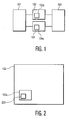
- the processing system includes a CPU 101 that receives instruction data for processing via an instruction cache memory 102 and other data for processing via a data cache memory 104, hereinbelow referred to as an instruction cache 102 and a data cache 104, respectively.
- Each cache, 102 and 104 is in communication with a main memory 103.
- the instruction cache 102 is for caching of only instruction data from the main memory 103, as it is required by the processor 101.
- Within the instruction cache 102 there is disposed an instruction cache controller 102a, including a fetching unit.
- the instruction cache controller 102a controls storage of data blocks within the instruction cache 102.
- the data cache 104 is for use in caching of data, which is other than instruction data, used for processing by the CPU 101.
- the data cache 104 has disposed therein a data cache controller 104a, including another fetching unit.
- a determination circuit 201 is disposed within the instruction cache 102.
- the determination circuit 201 is for use in analyzing of instruction data retrieved from main memory 103 and provided to the instruction cache 102 using an instruction analysis circuit.
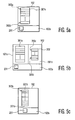
- a first program stream is shown 301 having a pre-interrupt portion 301a and a post interrupt portion 301b, with a second program stream 302 embedded therebetween.
- the second program stream is optionally in the form of an interrupt service request (ISR) program stream.
- An instruction pointer (IP) 303 is provided for use in maintaining an index at which the CPU 101 executes the first program stream 301 and the second program stream 302.
- Fig. 4 a process flowchart of the embodiment of the invention is shown.
- Fig. 5a illustrates a first program stream pre-interrupt portion 301a in execution from within the instruction cache 102 starting at instruction pointer (IP) address 303a. Fetches of instructions are performed from main memory 103 into the instruction cache 102 using the cache controller hardware 102a in order to reduce processor stall cycles during execution of the first program stream pre-interrupt portion 301a, from instruction pointer addresses 303a to 303b ( Fig. 5a ).
- a start of temporary cache indication step 402 Fig.
- the pre-interrupt portion 301a having an explicit instruction of a first type or by the determination circuit 201 determining at which point an instruction is provided indicative of an imminent execution of the second program stream 302 within the instruction cache 102.
- the determination circuit 201 instructs the cache controller 102a to partition the instruction cache 102 (step 403 Fig. 4 ) into a first memory portion 501a and second memory portion 501b ( Fig. 5b ).
- the first memory portion 501a a majority of cached instruction data associated with the first program stream pre-interrupt portion 301a is stored.
- the LRU process is preferably implemented by the cache controller 102a in order to free up memory space within the instruction cache 102 for use in enabling the creation of an available memory space that is to become the second memory portion 501b.
- the second memory portion 501b is used to implement a temporary cache 501b within the instruction cache 102.
- the instruction cache controller 102a implements a dedicated memory allocating process in order to free up memory space within the instruction cache memory 102 for use as the temporary cache 501b. For example, at least one predetermined cache way from the instruction cache 102 is set aside for use as the second memory portion 501b. That said, for an 8 way set associate cache, for example, three of the cache ways are set aside for implementing of the second memory portion 501b. Thus, the second memory portion is constrained to being 3/8 of the total available instruction cache memory space.
- the instruction cache controller 102a then preferably utilizes the LRU process for controlling the replacement of data blocks within these 3 cache ways, but is not used to select the cache ways that are to be used for implementing of the second memory portion 501b.
- the interrupted program is stored in the instruction cache memory 102 with a LRU indication, such that it is the immediate candidate for replacement when the least recently used cache way is used in further processing.
- step 404 Fig. 4
- the processor 101 executes the second program stream 302 stored in the temporary cache 501b from IP address 303c to 303d.
- this second memory portion 501b is not of sufficient size to accommodate the amount of data optimal for execution of this second program stream 302
- the LRU process is implemented in the temporary cache 501b in order to reduce the amount of fetches performed from main memory 103.
- the temporary cache 501b is eliminated, in step 405 ( Fig. 4 ), by the determination circuit 201 and the entire instruction cache 102 is again available for use by the post interrupt portion 301b of the first program stream 301 ( Fig. 5c ). Execution of the post interrupt portion 301b of the first program stream 301 is resumed at IP address 303e.
- IP address 303e IP address
- step 403 Fig. 4 Partitioning the instruction cache memory 102 into the first memory portion 501a and the second memory portion 501b, in the form of the temporary cache, (step 403 Fig. 4 ) realizes instruction processing advantages, such as a reduction in instruction cache trashing. Since the second program stream 302 typically does not contain loops instructions therein and is generally sequential in nature, instruction data fetched from main memory 103 for use in these generally sequential routines is rarely required subsequent to its execution. Therefore, the LRU process, executed by the instruction cache controller 102a, has an easy task of eliminating unnecessary instruction data from the instruction cache 102.
- the temporary cache 501b is advantageously relatively small, to act as a simple read ahead buffer for the second program stream 302, so that processor stall cycles are minimized for this second program stream 302, but not so large that a significant portion of the resulting first memory portion 501a is overwritten by implementing of the temporary cache 501b (step 403 Fig. 4 ). Since, the instruction cache first memory portion 501a contains data pertinent to the first program stream 301, overwriting a significant portion of this memory space is not advantageous because once execution of the first program stream 301b is resumed ( Fig.
- the instruction cache controller 102a fetches new instruction data into the temporary cache 501b for use by the second program stream 302 without overwriting a significant portion of the instruction data for use by the first program stream post interrupt portion 301b.
- the determination circuit 201 determines which portions of the instruction cache 102 to allocate to the temporary cache 501b, so that preferably a minimum amount of instruction data pertinent to the first program stream post interrupt portion 301b is overwritten.
- the CPU 101 again executes the post interrupt portion 301b of the first program stream at IP 303e ( Fig. 5c ).
- an amount instruction data pertinent thereto is still stored in the instruction cache 102.
- the instruction cache 102 has a size of 32kBytes, and assuming a 8-way set associativity, while restricting memory allocated to the temporary cache 501b to a that of a 4Kbyte cache way, this results in 28/32 of the original cache data still being pertinent to the first program stream post interrupt portion 301b after return from execution of the second program stream 302.
- Cache partitioning is implemented in two different manners in accordance with the invention.
- implementing instruction cache 102 partitioning is facilitated in hardware by having explicit instructions of a predetermined type that provide a start of temporary cache indication (step 402 Fig. 4 ) for triggering the determination circuit 201 for partitioning of the instruction cache.
- the determination circuit 201 reads an explicit instruction of a first type in the form of a start-of-temporary-cache instruction, the instruction cache 102 is partitioned into the first memory portion 501a and the temporary cache 501b ( Fig. 5b ), and the interrupt is processed.
- an explicit instruction of a second type in the form of an end-of-temporary-cache instruction, triggers the determination circuit 201 to free memory allocated to the temporary cache 501b so the entire instruction cache 102 is again useable by the first program stream post interrupt portion 301b.
- explicit instructions of the first and second types in the form of hardware triggered interrupts and return from interrupt instructions, respectively, are supportable in an analogous fashion as will be evident to those of skill in the art.
- the second program stream 302 includes instructions that are other than sequential in nature, for example, in the form of loop instructions embedded in second program stream 302. If the temporary cache 501b is not of a large enough size to accommodate caching of the whole second program stream 302, then multiple fetches are generated to main memory 103 in order to retrieve instruction data necessary for use in the execution of loop instructions embedded in the second program stream 302, the memory size allocated to the temporary cache 501b is too small, thus the second program stream 302 is larger than the working set of the temporary cache 501b.
- second program stream 302 blocks of instruction data are identified as being stored in certain memory address regions within the main memory 103.
- second program streams 302 are identified using addresses at which second program stream 302 instruction data is stored within the main memory 103.
- load indications are provided within the program stream that preferably enable a majority of all the second program stream instruction data to be stored in a same memory address region within main memory 103.
- any fetching from this memory address region automatically allows for partitioning of the instruction cache (step 403 Fig. 4 ) for storing of this second program stream instruction data 302 within the temporary cache 501b.
- dedicated instructions used for implementing of the temporary cache 501b are obviated.
- the determination circuit 201 thus performs a role of determining the type of instructions that are within the second program stream 302, and based on this determination, performs partitioning (step 403 Fig. 4 ) of the instruction cache memory 102. If the instruction cache memory 102 is not partitioned accordingly, then more stall cycles may be observed and hence the performance benefits are not realized.
- the information is optionally encoded within the instruction data for decoding by the determination circuit 201 instruction analysis circuit.
- instructions are included within instruction data stored in memory 102 that are indicative of whether to partition the instruction cache or not. These instructions then result in the determination circuit 201, or other software routines being executed by the processor, determine whether it is advantageous to perform partitioning of the instruction cache 102 or not.
- the cache memory 102 is optionally partitioned in dependence upon the type of instruction data being executed as a result of software determination. Where the software determines that partitioning of the cache is advantageous, this operation is performed in order to increase processing power of the CPU as well as to decrease power consumption of the cache memory circuit 102 and memory bandwidth requirements. More fetches performed from main memory 103 result in more power consumed by the circuits. Enabling and disabling logic gates, at a hardware level, used to implement the instruction cache memory 102 and main memory 103 realizes power savings.
- the temporary cache 501b is created in a fixed cache way in the instruction cache 102.
- the second memory portion 501b is only created in cache way 0.
- a single predetermined number of cache ways with a fixed size of 4 Kbytes are allocated for implementing the temporary cache 501b.
- fetching of 64 byte blocks is often not enough for the reduction of processor stall cycles.
- increasing the size of the fetch to two sequential 64 byte blocks is often preferable.
- multiple sequential 64 byte blocks may be prefetched.
Landscapes
- Engineering & Computer Science (AREA)
- Theoretical Computer Science (AREA)
- Software Systems (AREA)
- Physics & Mathematics (AREA)
- General Engineering & Computer Science (AREA)
- General Physics & Mathematics (AREA)
- Multimedia (AREA)
- Memory System Of A Hierarchy Structure (AREA)
- Power Sources (AREA)
Claims (22)
- Verwaltungsverfahren für einen Befehls-Cache mit den Schritten:- Bereitstellen einer Verarbeitungseinheit zum Ausführen von Befehlen;- Bereitstellen eines ersten Befehls-Cache-Speichers;- Bereitstellen erster in einem ersten Programmstrom innerhalb des ersten Befehls-Cache-Speicher zur Ausführung enthaltener Befehlsdaten;
gekennzeichnet durch:- Bereitstellen eines eine bevorstehende Ausführung eines zweiten Programmstroms innerhalb des ersten Befehl-Cache-Speichers anzeigenden Startbefehls für einen temporären Cache, wobei der Startbefehl für den temporären Cache zur Initiierung der Ausführung des zweiten Programmstroms dient;- Erzeugen eines temporären Caches innerhalb des ersten Befehl-Cache-Speichers auf Empfang des Startbefehls für den temporären Cache hin, wobei der temporäre Cache zur Verwendung beim Zwischenspeichern von Befehlsdaten, die beim Ausführen des zweiten Programmstroms verwendet werden, dient;- Ausführen von Befehlen innerhalb des zweiten Programmstroms; und- Entfernen des temporären Caches auf Ausführung eines Befehls zum Beenden der Ausführung des zweiten Programmstroms hin. - Verfahren gemäß Anspruch 1, mit dem Schritt: Bereitstellen eines Prozessors zur Ausführung von Befehlsdaten innerhalb des Befehls-Caches und zur Ausführung von Befehlsdaten innerhalb des temporären Caches zum Ausführen des zweiten Programmstroms.
- Verfahren gemäß Anspruch 1, wobei der zweite Programmstrom verringerte Befehls-Cache-Anforderungen im Vergleich zu den ersten Befehlsdaten innerhalb des ersten Befehl-Cache-Speichers besitzt.
- Verfahren gemäß Anspruch 1, welches einen Analyseschritt für Befehlsdaten innerhalb der ersten Befehlsdaten aufweist, zum Festzustellen, an welchem Punkt beim Ausführen der Befehle der Schritt des Erzeugens des temporären Caches durchzuführen ist.
- Verfahren gemäß Anspruch 4, wobei der Analyseschritt durch eine Softwareanwendung durchgeführt wird, die andere Befehlsdaten enthält als die ersten Befehlsdaten und der zweite Programmstrom.
- Verfahren gemäß Anspruch 4, wobei der Analyseschritt den Überprüfungsschritt aufweist, ob der erste Programmstrom oder der zweite Programmstrom Befehle einer vorbestimmten Art enthält.
- Verfahren gemäß Anspruch 6, wobei die Befehle vorbestimmter Art Interrupt-Befehle sind.
- Verfahren gemäß Anspruch 6, wobei die Befehle vorbestimmter Art ein Rücksprung von Interrupt-Befehlen sind.
- Verfahren gemäß Anspruch 4, wobei der Analyseschritt den Überprüfungsschritt aufweist, ob der zweite Programmstrom annähernd sequenziell ist, und wobei der Erzeugungsschritt in Abhängigkeit vom Überprüfungsschritt durchgeführt wird.
- Verfahren gemäß Anspruch 1, welches den Bereitstellungsschritt für einen Hauptspeicher zum Speichern des zweiten Programmstroms an einem Adressort aufweist, wobei der Startbefehl für den temporären Cache abhängig vom Adressort des zweiten Programmstroms ist.
- Verfahren gemäß Anspruch 1, wobei eine Größe des temporären Caches abhängig von einem in den ersten Befehlsdaten eingebetteten expliziten Befehl ist.
- Cache-Speicher mit:- einem Befehls-Cache-Speicher zum Zwischenspeichern von Befehlsdaten eines ersten Befehlsdatenstroms;
dadurch gekennzeichnet, dass der Cache-Speicher weiter aufweist:- eine Bestimmungsschaltung zum Bestimmen eines Vorliegens eines eine bevorstehende Ausführung eines zweiten Befehlsdatenstroms anzeigenden Startbefehls für einen temporären Cache und zum Unterteilen des Befehl-Cache-Speichers in einen ersten Speicherteil und einen temporären Speicherteil in Reaktion auf den Startbefehl für den temporären Cache und in Abhängigkeit vom Vorliegen des zweiten Befehlsdatenstroms, wobei ein Befehl innerhalb des zweiten Befehlsdatenstroms von einer identifizierbaren Art ist, wobei der erste Speicherteil zum Zwischenspeichern von Befehlen des ersten Befehlsdatenstroms dient und der temporäre Speicherteil zum Zwischenspeichern von Befehlen des zweiten Befehlsdatenstroms dient,- wobei die Bestimmungsschaltung weiter eingerichtet ist, den temporären Speicherteil auf Beendung des zweiten Befehlsdatenstroms hin zu entfernen. - Cache-Speicher gemäß Anspruch 12, wobei die Bestimmungsschaltung eine Hardware-Interrupt-Schaltung ist.
- Cache-Speicher gemäß Anspruch 12, wobei den zweiten Befehlsdaten innerhalb des ersten Befehlsdatenstroms ein expliziter Befehl vorausgeht.
- Cache-Speicher gemäß Anspruch 12, wobei die bekannten Eigenschaften des zweiten Befehlsdatenstroms Eigenschaften aufweisen, die identifizieren, dass der zweite Befehlsdatenstrom Befehle zur näherungsweisen sequenziellen Ausführung besitzt.
- Cache-Speicher gemäß Anspruch 12, wobei die bekannten Eigenschaften des zweiten Befehlsdatenstroms Eigenschaften aufweisen, die identifizieren, dass der zweite Befehlsdatenstrom Befehle zur Ausführung in Reihe besitzt.
- Cache-Speicher gemäß Anspruch 12, wobei der zweite Befehlsdatenstrom reduzierte Cache-Anforderungen gegenüber dem ersten Befehlsdatenstrom besitzt.
- Cache-Speicher gemäß Anspruch 12, wobei die Bestimmungsschaltung eine Befehlsanalyseschaltung zum Identifizieren von Befehlen einer vorbestimmten Art zur Erzeugung des temporären Speicherteils aufweist.
- Cache-Speicher gemäß Anspruch 18, wobei die Befehle vorbestimmter Art einen expliziten Befehl aufweisen.
- Cache-Speicher gemäß Anspruch 12, wobei die Bestimmungsschaltung eine Befehlsanalyseschaltung zum Identifizieren von Befehlen einer vorbestimmten Art zum Beenden des temporären Speicherteils aufweist.
- Cache-Speicher gemäß Anspruch 20, wobei die Befehle vorbestimmter Art einen Rücksprung von einem Interrupt-Befehl aufweisen.
- Cache-Speicher gemäß Anspruch 20, wobei der Befehl vorbestimmter Art ein expliziter Befehl einer ersten oder einer zweiten Art ist.
Applications Claiming Priority (3)
| Application Number | Priority Date | Filing Date | Title |
|---|---|---|---|
| US44887103P | 2003-02-24 | 2003-02-24 | |
| US448871P | 2003-02-24 | ||
| PCT/IB2004/000455 WO2004075066A2 (en) | 2003-02-24 | 2004-02-23 | Reducing cache trashing of certain pieces |
Publications (2)
| Publication Number | Publication Date |
|---|---|
| EP1599803A2 EP1599803A2 (de) | 2005-11-30 |
| EP1599803B1 true EP1599803B1 (de) | 2009-09-30 |
Family
ID=32908665
Family Applications (1)
| Application Number | Title | Priority Date | Filing Date |
|---|---|---|---|
| EP04713597A Expired - Lifetime EP1599803B1 (de) | 2003-02-24 | 2004-02-23 | Cache-speicher-trashings-verringerung von bestimmten code-stücken |
Country Status (8)
| Country | Link |
|---|---|
| US (1) | US7353337B2 (de) |
| EP (1) | EP1599803B1 (de) |
| JP (1) | JP2006518896A (de) |
| KR (1) | KR100985239B1 (de) |
| CN (1) | CN1777875B (de) |
| AT (1) | ATE444526T1 (de) |
| DE (1) | DE602004023372D1 (de) |
| WO (1) | WO2004075066A2 (de) |
Families Citing this family (11)
| Publication number | Priority date | Publication date | Assignee | Title |
|---|---|---|---|---|
| US7263587B1 (en) * | 2003-06-27 | 2007-08-28 | Zoran Corporation | Unified memory controller |
| KR100735552B1 (ko) | 2005-09-23 | 2007-07-04 | 삼성전자주식회사 | 코드 메모리 상의 프로그램의 코드 크기를 줄이는 방법 |
| US7689772B2 (en) * | 2006-05-04 | 2010-03-30 | Intel Corporation | Power-performance modulation in caches using a smart least recently used scheme |
| US7747820B2 (en) * | 2007-06-15 | 2010-06-29 | Microsoft Corporation | Managing working set use of a cache via page coloring |
| CN101753282B (zh) * | 2008-12-22 | 2013-06-19 | 电信科学技术研究院 | 一种进程缓存的配置和处理的方法及系统 |
| FR2962567B1 (fr) * | 2010-07-12 | 2013-04-26 | Bull Sas | Procede d'optimisation d'acces memoire, lors de la reprise d'execution d'une application, dans un microprocesseur comprenant plusieurs coeurs logiques et programme d'ordinateur mettant en oeuvre un tel procede |
| US9104532B2 (en) * | 2012-12-14 | 2015-08-11 | International Business Machines Corporation | Sequential location accesses in an active memory device |
| WO2014143036A1 (en) | 2013-03-15 | 2014-09-18 | Intel Corporation | Method for pinning data in large cache in multi-level memory system |
| US9558124B2 (en) * | 2013-11-08 | 2017-01-31 | Seagate Technology Llc | Data storage system with passive partitioning in a secondary memory |
| CN105706049B (zh) * | 2014-01-27 | 2019-04-16 | 上海兆芯集成电路有限公司 | 操作系统例行程序的预测历程储存器的部分使用 |
| US10235203B1 (en) | 2014-03-31 | 2019-03-19 | EMC IP Holding Company LLC | Techniques for increasing storage system performance in processor-bound workloads with large working sets and poor spatial locality |
Family Cites Families (14)
| Publication number | Priority date | Publication date | Assignee | Title |
|---|---|---|---|---|
| US4463424A (en) * | 1981-02-19 | 1984-07-31 | International Business Machines Corporation | Method for dynamically allocating LRU/MRU managed memory among concurrent sequential processes |
| EP0389151A3 (de) * | 1989-03-22 | 1992-06-03 | International Business Machines Corporation | System und Verfahren für die Verwaltung eines verteilten Cache-Speichers |
| US5394531A (en) * | 1989-04-03 | 1995-02-28 | International Business Machines Corporation | Dynamic storage allocation system for a prioritized cache |
| EP0442474B1 (de) * | 1990-02-13 | 1997-07-23 | Sanyo Electric Co., Ltd. | Vorrichtung und Verfahren zum Steuern eines Cache-Speichers |
| JPH0799508B2 (ja) * | 1990-10-15 | 1995-10-25 | インターナショナル・ビジネス・マシーンズ・コーポレイション | キャッシュ記憶機構を動的に区分する方法およびキャッシュ記憶機構システム |
| US5537635A (en) * | 1994-04-04 | 1996-07-16 | International Business Machines Corporation | Method and system for assignment of reclaim vectors in a partitioned cache with a virtual minimum partition size |
| US5696932A (en) * | 1995-05-16 | 1997-12-09 | International Business Machines Corporation | Method and system for estimating minumun requirements on a cache in a computer based storage system |
| US5893920A (en) * | 1996-09-30 | 1999-04-13 | International Business Machines Corporation | System and method for cache management in mobile user file systems |
| GB9701960D0 (en) * | 1997-01-30 | 1997-03-19 | Sgs Thomson Microelectronics | A cache system |
| EP0856798B1 (de) * | 1997-01-30 | 2004-09-29 | STMicroelectronics Limited | Cachespeichersystem |
| US6260114B1 (en) * | 1997-12-30 | 2001-07-10 | Mcmz Technology Innovations, Llc | Computer cache memory windowing |
| US6370619B1 (en) * | 1998-06-22 | 2002-04-09 | Oracle Corporation | Managing partitioned cache |
| US6349363B2 (en) * | 1998-12-08 | 2002-02-19 | Intel Corporation | Multi-section cache with different attributes for each section |
| US6898694B2 (en) * | 2001-06-28 | 2005-05-24 | Intel Corporation | High instruction fetch bandwidth in multithread processor using temporary instruction cache to deliver portion of cache line in subsequent clock cycle |
-
2004
- 2004-02-23 US US10/546,757 patent/US7353337B2/en not_active Expired - Lifetime
- 2004-02-23 JP JP2006502458A patent/JP2006518896A/ja active Pending
- 2004-02-23 WO PCT/IB2004/000455 patent/WO2004075066A2/en not_active Ceased
- 2004-02-23 KR KR1020057015715A patent/KR100985239B1/ko not_active Expired - Fee Related
- 2004-02-23 EP EP04713597A patent/EP1599803B1/de not_active Expired - Lifetime
- 2004-02-23 AT AT04713597T patent/ATE444526T1/de not_active IP Right Cessation
- 2004-02-23 DE DE602004023372T patent/DE602004023372D1/de not_active Expired - Lifetime
- 2004-02-23 CN CN2004800109564A patent/CN1777875B/zh not_active Expired - Fee Related
Also Published As
| Publication number | Publication date |
|---|---|
| KR20050115875A (ko) | 2005-12-08 |
| EP1599803A2 (de) | 2005-11-30 |
| CN1777875B (zh) | 2010-04-28 |
| WO2004075066A2 (en) | 2004-09-02 |
| WO2004075066A8 (en) | 2005-04-07 |
| KR100985239B1 (ko) | 2010-10-04 |
| ATE444526T1 (de) | 2009-10-15 |
| DE602004023372D1 (de) | 2009-11-12 |
| US20060179225A1 (en) | 2006-08-10 |
| CN1777875A (zh) | 2006-05-24 |
| WO2004075066A3 (en) | 2004-10-07 |
| US7353337B2 (en) | 2008-04-01 |
| JP2006518896A (ja) | 2006-08-17 |
Similar Documents
| Publication | Publication Date | Title |
|---|---|---|
| US8250332B2 (en) | Partitioned replacement for cache memory | |
| US5838945A (en) | Tunable software control of harvard architecture cache memories using prefetch instructions | |
| US5829025A (en) | Computer system and method of allocating cache memories in a multilevel cache hierarchy utilizing a locality hint within an instruction | |
| JP3816586B2 (ja) | 先取り命令を生成する方法とシステム | |
| EP2095243B1 (de) | Konfigurierbarer cache für einen mikroprozessor | |
| US7895399B2 (en) | Computer system and control method for controlling processor execution of a prefetech command | |
| US7707359B2 (en) | Method and apparatus for selectively prefetching based on resource availability | |
| US20070204107A1 (en) | Cache memory background preprocessing | |
| EP2092429B1 (de) | Konfigurierbarer cache für einen mikroprozessor | |
| US6578065B1 (en) | Multi-threaded processing system and method for scheduling the execution of threads based on data received from a cache memory | |
| JP2005539321A (ja) | データ処理システムの外部および内部命令セット | |
| CA2282373A1 (en) | Computer cache memory windowing | |
| CN1255986A (zh) | 基于惩罚的高速缓冲存储器和置换技术 | |
| EP2495662B1 (de) | Konfigurierbarer Cache für einen Mikroprozessor | |
| EP1599803B1 (de) | Cache-speicher-trashings-verringerung von bestimmten code-stücken | |
| JP2006516168A (ja) | ストライド予測テーブルにアドレスするためにキャッシュミスパターンを使用する方法 | |
| WO2001038970A2 (en) | Buffer memories, methods and systems for buffering having seperate buffer memories for each of a plurality of tasks | |
| US8266379B2 (en) | Multithreaded processor with multiple caches | |
| US6745296B2 (en) | System and method for providing cacheable smram | |
| US8429383B2 (en) | Multi-processor computing system having a JAVA stack machine and a RISC-based processor | |
| US20020174300A1 (en) | Data processor and data processing method | |
| US20260093635A1 (en) | Translation lookaside buffer prewarming | |
| JP2003228518A (ja) | キャッシュシステムの制御方法 |
Legal Events
| Date | Code | Title | Description |
|---|---|---|---|
| PUAI | Public reference made under article 153(3) epc to a published international application that has entered the european phase |
Free format text: ORIGINAL CODE: 0009012 |
|
| 17P | Request for examination filed |
Effective date: 20050926 |
|
| AK | Designated contracting states |
Kind code of ref document: A2 Designated state(s): AT BE BG CH CY CZ DE DK EE ES FI FR GB GR HU IE IT LI LU MC NL PT RO SE SI SK TR |
|
| AX | Request for extension of the european patent |
Extension state: AL LT LV MK |
|
| DAX | Request for extension of the european patent (deleted) | ||
| RAP1 | Party data changed (applicant data changed or rights of an application transferred) |
Owner name: NXP B.V. |
|
| RAP1 | Party data changed (applicant data changed or rights of an application transferred) |
Owner name: NXP B.V. |
|
| GRAP | Despatch of communication of intention to grant a patent |
Free format text: ORIGINAL CODE: EPIDOSNIGR1 |
|
| GRAS | Grant fee paid |
Free format text: ORIGINAL CODE: EPIDOSNIGR3 |
|
| GRAA | (expected) grant |
Free format text: ORIGINAL CODE: 0009210 |
|
| AK | Designated contracting states |
Kind code of ref document: B1 Designated state(s): AT BE BG CH CY CZ DE DK EE ES FI FR GB GR HU IE IT LI LU MC NL PT RO SE SI SK TR |
|
| REG | Reference to a national code |
Ref country code: GB Ref legal event code: FG4D Ref country code: CH Ref legal event code: EP |
|
| REG | Reference to a national code |
Ref country code: IE Ref legal event code: FG4D |
|
| REF | Corresponds to: |
Ref document number: 602004023372 Country of ref document: DE Date of ref document: 20091112 Kind code of ref document: P |
|
| PG25 | Lapsed in a contracting state [announced via postgrant information from national office to epo] |
Ref country code: SE Free format text: LAPSE BECAUSE OF FAILURE TO SUBMIT A TRANSLATION OF THE DESCRIPTION OR TO PAY THE FEE WITHIN THE PRESCRIBED TIME-LIMIT Effective date: 20090930 Ref country code: FI Free format text: LAPSE BECAUSE OF FAILURE TO SUBMIT A TRANSLATION OF THE DESCRIPTION OR TO PAY THE FEE WITHIN THE PRESCRIBED TIME-LIMIT Effective date: 20090930 |
|
| PG25 | Lapsed in a contracting state [announced via postgrant information from national office to epo] |
Ref country code: SI Free format text: LAPSE BECAUSE OF FAILURE TO SUBMIT A TRANSLATION OF THE DESCRIPTION OR TO PAY THE FEE WITHIN THE PRESCRIBED TIME-LIMIT Effective date: 20090930 |
|
| NLV1 | Nl: lapsed or annulled due to failure to fulfill the requirements of art. 29p and 29m of the patents act | ||
| PG25 | Lapsed in a contracting state [announced via postgrant information from national office to epo] |
Ref country code: RO Free format text: LAPSE BECAUSE OF FAILURE TO SUBMIT A TRANSLATION OF THE DESCRIPTION OR TO PAY THE FEE WITHIN THE PRESCRIBED TIME-LIMIT Effective date: 20090930 Ref country code: CZ Free format text: LAPSE BECAUSE OF FAILURE TO SUBMIT A TRANSLATION OF THE DESCRIPTION OR TO PAY THE FEE WITHIN THE PRESCRIBED TIME-LIMIT Effective date: 20090930 Ref country code: PT Free format text: LAPSE BECAUSE OF FAILURE TO SUBMIT A TRANSLATION OF THE DESCRIPTION OR TO PAY THE FEE WITHIN THE PRESCRIBED TIME-LIMIT Effective date: 20100201 Ref country code: EE Free format text: LAPSE BECAUSE OF FAILURE TO SUBMIT A TRANSLATION OF THE DESCRIPTION OR TO PAY THE FEE WITHIN THE PRESCRIBED TIME-LIMIT Effective date: 20090930 Ref country code: ES Free format text: LAPSE BECAUSE OF FAILURE TO SUBMIT A TRANSLATION OF THE DESCRIPTION OR TO PAY THE FEE WITHIN THE PRESCRIBED TIME-LIMIT Effective date: 20100110 |
|
| PG25 | Lapsed in a contracting state [announced via postgrant information from national office to epo] |
Ref country code: SK Free format text: LAPSE BECAUSE OF FAILURE TO SUBMIT A TRANSLATION OF THE DESCRIPTION OR TO PAY THE FEE WITHIN THE PRESCRIBED TIME-LIMIT Effective date: 20090930 Ref country code: CY Free format text: LAPSE BECAUSE OF FAILURE TO SUBMIT A TRANSLATION OF THE DESCRIPTION OR TO PAY THE FEE WITHIN THE PRESCRIBED TIME-LIMIT Effective date: 20090930 |
|
| PG25 | Lapsed in a contracting state [announced via postgrant information from national office to epo] |
Ref country code: BE Free format text: LAPSE BECAUSE OF FAILURE TO SUBMIT A TRANSLATION OF THE DESCRIPTION OR TO PAY THE FEE WITHIN THE PRESCRIBED TIME-LIMIT Effective date: 20090930 Ref country code: AT Free format text: LAPSE BECAUSE OF FAILURE TO SUBMIT A TRANSLATION OF THE DESCRIPTION OR TO PAY THE FEE WITHIN THE PRESCRIBED TIME-LIMIT Effective date: 20090930 |
|
| PG25 | Lapsed in a contracting state [announced via postgrant information from national office to epo] |
Ref country code: NL Free format text: LAPSE BECAUSE OF FAILURE TO SUBMIT A TRANSLATION OF THE DESCRIPTION OR TO PAY THE FEE WITHIN THE PRESCRIBED TIME-LIMIT Effective date: 20090930 Ref country code: DK Free format text: LAPSE BECAUSE OF FAILURE TO SUBMIT A TRANSLATION OF THE DESCRIPTION OR TO PAY THE FEE WITHIN THE PRESCRIBED TIME-LIMIT Effective date: 20090930 |
|
| PLBE | No opposition filed within time limit |
Free format text: ORIGINAL CODE: 0009261 |
|
| STAA | Information on the status of an ep patent application or granted ep patent |
Free format text: STATUS: NO OPPOSITION FILED WITHIN TIME LIMIT |
|
| 26N | No opposition filed |
Effective date: 20100701 |
|
| REG | Reference to a national code |
Ref country code: CH Ref legal event code: PL |
|
| PG25 | Lapsed in a contracting state [announced via postgrant information from national office to epo] |
Ref country code: LI Free format text: LAPSE BECAUSE OF NON-PAYMENT OF DUE FEES Effective date: 20100228 Ref country code: CH Free format text: LAPSE BECAUSE OF NON-PAYMENT OF DUE FEES Effective date: 20100228 Ref country code: GR Free format text: LAPSE BECAUSE OF FAILURE TO SUBMIT A TRANSLATION OF THE DESCRIPTION OR TO PAY THE FEE WITHIN THE PRESCRIBED TIME-LIMIT Effective date: 20091231 Ref country code: MC Free format text: LAPSE BECAUSE OF NON-PAYMENT OF DUE FEES Effective date: 20100301 |
|
| PG25 | Lapsed in a contracting state [announced via postgrant information from national office to epo] |
Ref country code: IE Free format text: LAPSE BECAUSE OF NON-PAYMENT OF DUE FEES Effective date: 20100223 |
|
| PG25 | Lapsed in a contracting state [announced via postgrant information from national office to epo] |
Ref country code: IT Free format text: LAPSE BECAUSE OF FAILURE TO SUBMIT A TRANSLATION OF THE DESCRIPTION OR TO PAY THE FEE WITHIN THE PRESCRIBED TIME-LIMIT Effective date: 20090930 |
|
| REG | Reference to a national code |
Ref country code: DE Ref legal event code: R082 Ref document number: 602004023372 Country of ref document: DE Representative=s name: MUELLER - HOFFMANN & PARTNER PATENTANWAELTE, DE |
|
| REG | Reference to a national code |
Ref country code: GB Ref legal event code: 732E Free format text: REGISTERED BETWEEN 20120301 AND 20120307 |
|
| REG | Reference to a national code |
Ref country code: DE Ref legal event code: R082 Ref document number: 602004023372 Country of ref document: DE Representative=s name: MUELLER HOFFMANN & PARTNER PATENTANWAELTE MBB, DE Effective date: 20120326 Ref country code: DE Ref legal event code: R081 Ref document number: 602004023372 Country of ref document: DE Owner name: NYTELL SOFTWARE LLC, WILMINGTON, US Free format text: FORMER OWNER: NXP B.V., EINDHOVEN, NL Effective date: 20120326 Ref country code: DE Ref legal event code: R081 Ref document number: 602004023372 Country of ref document: DE Owner name: NYTELL SOFTWARE LLC, US Free format text: FORMER OWNER: NXP B.V., EINDHOVEN, NL Effective date: 20120326 Ref country code: DE Ref legal event code: R082 Ref document number: 602004023372 Country of ref document: DE Representative=s name: MUELLER - HOFFMANN & PARTNER PATENTANWAELTE, DE Effective date: 20120326 |
|
| PG25 | Lapsed in a contracting state [announced via postgrant information from national office to epo] |
Ref country code: HU Free format text: LAPSE BECAUSE OF FAILURE TO SUBMIT A TRANSLATION OF THE DESCRIPTION OR TO PAY THE FEE WITHIN THE PRESCRIBED TIME-LIMIT Effective date: 20100401 Ref country code: LU Free format text: LAPSE BECAUSE OF NON-PAYMENT OF DUE FEES Effective date: 20100223 Ref country code: BG Free format text: LAPSE BECAUSE OF FAILURE TO SUBMIT A TRANSLATION OF THE DESCRIPTION OR TO PAY THE FEE WITHIN THE PRESCRIBED TIME-LIMIT Effective date: 20090930 |
|
| PG25 | Lapsed in a contracting state [announced via postgrant information from national office to epo] |
Ref country code: TR Free format text: LAPSE BECAUSE OF FAILURE TO SUBMIT A TRANSLATION OF THE DESCRIPTION OR TO PAY THE FEE WITHIN THE PRESCRIBED TIME-LIMIT Effective date: 20090930 |
|
| REG | Reference to a national code |
Ref country code: FR Ref legal event code: PLFP Year of fee payment: 12 |
|
| PGFP | Annual fee paid to national office [announced via postgrant information from national office to epo] |
Ref country code: DE Payment date: 20150227 Year of fee payment: 12 |
|
| REG | Reference to a national code |
Ref country code: FR Ref legal event code: PLFP Year of fee payment: 13 |
|
| REG | Reference to a national code |
Ref country code: DE Ref legal event code: R119 Ref document number: 602004023372 Country of ref document: DE |
|
| REG | Reference to a national code |
Ref country code: FR Ref legal event code: PLFP Year of fee payment: 14 |
|
| PG25 | Lapsed in a contracting state [announced via postgrant information from national office to epo] |
Ref country code: DE Free format text: LAPSE BECAUSE OF NON-PAYMENT OF DUE FEES Effective date: 20160901 |
|
| REG | Reference to a national code |
Ref country code: FR Ref legal event code: PLFP Year of fee payment: 15 |
|
| PGFP | Annual fee paid to national office [announced via postgrant information from national office to epo] |
Ref country code: FR Payment date: 20210120 Year of fee payment: 18 |
|
| PGFP | Annual fee paid to national office [announced via postgrant information from national office to epo] |
Ref country code: GB Payment date: 20210129 Year of fee payment: 18 |
|
| GBPC | Gb: european patent ceased through non-payment of renewal fee |
Effective date: 20220223 |
|
| PG25 | Lapsed in a contracting state [announced via postgrant information from national office to epo] |
Ref country code: FR Free format text: LAPSE BECAUSE OF NON-PAYMENT OF DUE FEES Effective date: 20220228 |
|
| PG25 | Lapsed in a contracting state [announced via postgrant information from national office to epo] |
Ref country code: GB Free format text: LAPSE BECAUSE OF NON-PAYMENT OF DUE FEES Effective date: 20220223 |